EP1928005A2 - Micro-electromechanical system based arc-less switching with circuity for absorbing electrical energy during a fault condition - Google Patents
Micro-electromechanical system based arc-less switching with circuity for absorbing electrical energy during a fault condition Download PDFInfo
- Publication number
- EP1928005A2 EP1928005A2 EP07110553A EP07110553A EP1928005A2 EP 1928005 A2 EP1928005 A2 EP 1928005A2 EP 07110553 A EP07110553 A EP 07110553A EP 07110553 A EP07110553 A EP 07110553A EP 1928005 A2 EP1928005 A2 EP 1928005A2
- Authority
- EP
- European Patent Office
- Prior art keywords
- pulse
- circuit
- switch
- current
- energy
- Prior art date
- Legal status (The legal status is an assumption and is not a legal conclusion. Google has not performed a legal analysis and makes no representation as to the accuracy of the status listed.)
- Granted
Links
- 230000004044 response Effects 0.000 claims abstract description 26
- 230000015572 biosynthetic process Effects 0.000 claims abstract description 11
- 239000003990 capacitor Substances 0.000 claims description 56
- 230000000452 restraining effect Effects 0.000 claims description 2
- 238000000034 method Methods 0.000 description 23
- 230000001629 suppression Effects 0.000 description 18
- 238000010586 diagram Methods 0.000 description 15
- 230000008569 process Effects 0.000 description 10
- 230000007423 decrease Effects 0.000 description 9
- 238000001514 detection method Methods 0.000 description 8
- 230000006870 function Effects 0.000 description 7
- 230000002441 reversible effect Effects 0.000 description 6
- 230000009471 action Effects 0.000 description 5
- 238000012546 transfer Methods 0.000 description 5
- 230000001419 dependent effect Effects 0.000 description 4
- 230000000977 initiatory effect Effects 0.000 description 4
- 238000005457 optimization Methods 0.000 description 4
- 230000009467 reduction Effects 0.000 description 4
- 230000002829 reductive effect Effects 0.000 description 4
- 238000000926 separation method Methods 0.000 description 4
- 230000001960 triggered effect Effects 0.000 description 4
- 239000013598 vector Substances 0.000 description 4
- 230000003466 anti-cipated effect Effects 0.000 description 3
- 230000008859 change Effects 0.000 description 3
- 230000003247 decreasing effect Effects 0.000 description 3
- 238000013461 design Methods 0.000 description 2
- 230000007246 mechanism Effects 0.000 description 2
- 238000012986 modification Methods 0.000 description 2
- 230000004048 modification Effects 0.000 description 2
- 230000003071 parasitic effect Effects 0.000 description 2
- 230000001681 protective effect Effects 0.000 description 2
- 230000001052 transient effect Effects 0.000 description 2
- 238000010521 absorption reaction Methods 0.000 description 1
- 238000013459 approach Methods 0.000 description 1
- 230000008901 benefit Effects 0.000 description 1
- 230000000903 blocking effect Effects 0.000 description 1
- 239000002131 composite material Substances 0.000 description 1
- 238000013016 damping Methods 0.000 description 1
- 238000012938 design process Methods 0.000 description 1
- 230000001627 detrimental effect Effects 0.000 description 1
- 230000003467 diminishing effect Effects 0.000 description 1
- 230000000694 effects Effects 0.000 description 1
- 238000005516 engineering process Methods 0.000 description 1
- 230000006872 improvement Effects 0.000 description 1
- 230000001939 inductive effect Effects 0.000 description 1
- 230000005764 inhibitory process Effects 0.000 description 1
- 230000003993 interaction Effects 0.000 description 1
- 230000000670 limiting effect Effects 0.000 description 1
- 238000004519 manufacturing process Methods 0.000 description 1
- 229910044991 metal oxide Inorganic materials 0.000 description 1
- 150000004706 metal oxides Chemical class 0.000 description 1
- 238000012544 monitoring process Methods 0.000 description 1
- 238000004806 packaging method and process Methods 0.000 description 1
- 230000021715 photosynthesis, light harvesting Effects 0.000 description 1
- 238000012163 sequencing technique Methods 0.000 description 1
- 238000007493 shaping process Methods 0.000 description 1
- 238000004088 simulation Methods 0.000 description 1
- 230000003068 static effect Effects 0.000 description 1
- 239000000758 substrate Substances 0.000 description 1
Images


Classifications
-
- H—ELECTRICITY
- H01—ELECTRIC ELEMENTS
- H01H—ELECTRIC SWITCHES; RELAYS; SELECTORS; EMERGENCY PROTECTIVE DEVICES
- H01H59/00—Electrostatic relays; Electro-adhesion relays
- H01H59/0009—Electrostatic relays; Electro-adhesion relays making use of micromechanics
-
- H—ELECTRICITY
- H01—ELECTRIC ELEMENTS
- H01H—ELECTRIC SWITCHES; RELAYS; SELECTORS; EMERGENCY PROTECTIVE DEVICES
- H01H9/00—Details of switching devices, not covered by groups H01H1/00 - H01H7/00
- H01H9/54—Circuit arrangements not adapted to a particular application of the switching device and for which no provision exists elsewhere
- H01H9/541—Contacts shunted by semiconductor devices
- H01H9/542—Contacts shunted by static switch means
- H01H2009/543—Contacts shunted by static switch means third parallel branch comprising an energy absorber, e.g. MOV, PTC, Zener
-
- H—ELECTRICITY
- H01—ELECTRIC ELEMENTS
- H01H—ELECTRIC SWITCHES; RELAYS; SELECTORS; EMERGENCY PROTECTIVE DEVICES
- H01H71/00—Details of the protective switches or relays covered by groups H01H73/00 - H01H83/00
- H01H2071/008—Protective switches or relays using micromechanics
-
- H—ELECTRICITY
- H01—ELECTRIC ELEMENTS
- H01H—ELECTRIC SWITCHES; RELAYS; SELECTORS; EMERGENCY PROTECTIVE DEVICES
- H01H9/00—Details of switching devices, not covered by groups H01H1/00 - H01H7/00
- H01H9/54—Circuit arrangements not adapted to a particular application of the switching device and for which no provision exists elsewhere
- H01H9/541—Contacts shunted by semiconductor devices
-
- H—ELECTRICITY
- H03—ELECTRONIC CIRCUITRY
- H03K—PULSE TECHNIQUE
- H03K17/00—Electronic switching or gating, i.e. not by contact-making and –breaking
- H03K17/08—Modifications for protecting switching circuit against overcurrent or overvoltage
- H03K17/081—Modifications for protecting switching circuit against overcurrent or overvoltage without feedback from the output circuit to the control circuit
- H03K17/0814—Modifications for protecting switching circuit against overcurrent or overvoltage without feedback from the output circuit to the control circuit by measures taken in the output circuit
- H03K17/08142—Modifications for protecting switching circuit against overcurrent or overvoltage without feedback from the output circuit to the control circuit by measures taken in the output circuit in field-effect transistor switches
-
- H—ELECTRICITY
- H03—ELECTRONIC CIRCUITRY
- H03K—PULSE TECHNIQUE
- H03K17/00—Electronic switching or gating, i.e. not by contact-making and –breaking
- H03K17/08—Modifications for protecting switching circuit against overcurrent or overvoltage
- H03K17/082—Modifications for protecting switching circuit against overcurrent or overvoltage by feedback from the output to the control circuit
- H03K17/0822—Modifications for protecting switching circuit against overcurrent or overvoltage by feedback from the output to the control circuit in field-effect transistor switches
Definitions
- the system includes switching circuitry comprising a micro-electromechanical system switch configured to switch the system from a first switching state to a second switching state.
- An arc suppression circuitry is coupled to the switching circuitry, wherein the arc suppression circuitry is configured to suppress an arc formation between contacts of the micro-electromechanical system switch.
- Detection circuitry is coupled to the arc suppression circuitry and configured to determine existence of a fault condition.
- the first MEMS switch 20 may be coupled in parallel across midpoints of the balanced diode bridge 28.
- the midpoints of the balanced diode bridge may include a first midpoint located between the first and second diodes 30, 32 and a second midpoint located between the third and fourth diodes 34, 36.
- the first MEMS switch 20 and the balanced diode bridge 28 may be tightly packaged to facilitate minimization of parasitic inductance caused by the balanced diode bridge 28 and in particular, the connections to the MEMS switch 20.
- the pulse circuit 52 may include a pulse switch 54 and a pulse capacitor C PULSE 56 series coupled to the pulse switch 54. Further, the pulse circuit may also include a pulse inductance L PULSE 58 and a first diode D P 60 coupled in series with the pulse switch 54. The pulse inductance L PULSE 58, the diode D P 60, the pulse switch 54 and the pulse capacitor C PULSE 56 may be coupled in series to form a first branch of the pulse circuit 52, where the components of the first branch may be configured to facilitate pulse current shaping and timing. Also, reference numeral 62 is representative of a pulse circuit current I PULSE that may flow through the pulse circuit 52.
- triggering of the pulse switch 54 may include controlling a timing of the pulse circuit current I PULSE 62 through the balanced diode bridge 28 to facilitate creating a lower impedance path as compared to the impedance of a path through the contacts of the MEMS switch 20 during an opening interval.
- the pulse switch 54 may be triggered such that a desired voltage drop is presented across the contacts of the MEMS switch 20.
- the pulse switch 54 may be a solid-state switch that may be configured to have switching speeds in the range of nanoseconds to microseconds, for example.
- the switching speed of the pulse switch 54 should be relatively fast compared to the anticipated rise time of the load current in a fault condition.
- the current rating of the MEMS switch 20 is dependent on the rate of rise of the load current, which in turn is dependent on the inductance L LOAD 46 and the bus supply voltage V BUS 44 in the load circuit 40 as previously noted.
- the MEMS switch 20 may be appropriately rated to handle a larger load current I LOAD 50 if the load current
- the pulse circuit current I PULSE 62 may resonantly decrease to a zero value and to maintain the zero value due to the reverse blocking action of the diode bridge 28 and the diode D P 60.
- a circuit arrangement embodying aspects of the present invention should result in a reduced amount of fault let-through current and lower breaker energy dissipation.
- diode bridge 28 and MEMS switch 20 may be packaged to be closely integrated with one another (e.g., composite packaging) for reduction of parasitic inductance in the diode bridge and the respective interconnections to the MEMS switch. This incrementally reduces the amount of electrical energy that may be stored in such interconnections.
Abstract
Description
- Embodiments of the invention relate generally to a switching device for switching off a current in a current path, and more particularly to micro-electromechanical system based switching devices.
- A circuit breaker is an electrical device designed to protect electrical equipment from damage caused by faults in the circuit. Traditionally, most conventional circuit breakers include bulky electromechanical switches. Unfortunately, these conventional circuit breakers are large in size thereby necessitating use of a large force to activate the switching mechanism. Additionally, the switches of these circuit breakers generally operate at relatively slow speeds. Furthermore, these circuit breakers are disadvantageously complex to build and thus expensive to fabricate. In addition, when contacts of the switching mechanism in conventional circuit breakers are physically separated, an arc is typically formed therebetween which continues to carry current until the current in the circuit ceases. Moreover, energy associated with the arc may seriously damage the contacts and/or present a burn hazard to personnel.
- As an alternative to slow electromechanical switches, fast solid-state switches have been employed in high speed switching applications. As will be appreciated, these solid-state switches switch between a conducting state and a non-conducting state through controlled application of a voltage or bias. For example, by reverse biasing a solid-state switch, the switch may be transitioned into a non-conducting state. However, since solid-state switches do not create a physical gap between contacts when they are switched into a non-conducing state, they experience leakage current. Furthermore, due to internal resistances, when solid-state switches operate in a conducting state, they experience a voltage drop. Both the voltage drop and leakage current contribute to the generation of excess heat under normal operating circumstances, which may be detrimental to switch performance and life. Moreover, due at least in part to the inherent leakage current associated with solid-state switches, their use in circuit breaker applications is not possible.
- Briefly, in accordance with aspects of the present technique, a system is presented. The system includes a micro-electromechanical system switch. A balanced diode bridge is configured to suppress arc formation between contacts of the micro-electromechanical system switch. A pulse circuit is coupled to the balanced diode bridge. The pulse circuit comprises a pulse capacitor adapted to form a pulse signal for causing flow of a pulse current through the balanced diode bridge. The pulse signal is generated in response to a fault condition in a load circuit coupled to the micro-electromechanical system switch. An energy-absorbing circuitry is coupled in a parallel circuit with the pulse circuit. The energy-absorbing circuitry comprises an energy-absorbing capacitor adapted to absorb electrical energy resulting from the fault condition without affecting a pulse signal formation by the pulse circuit.
- In accordance with further aspects of the present technique a system is presented. The system includes switching circuitry comprising a micro-electromechanical system switch configured to switch the system from a first switching state to a second switching state. An arc suppression circuitry is coupled to the switching circuitry, wherein the arc suppression circuitry is configured to suppress an arc formation between contacts of the micro-electromechanical system switch. Detection circuitry is coupled to the arc suppression circuitry and configured to determine existence of a fault condition. A pulse circuit is coupled to the arc suppression circuitry and the detection circuitry, wherein the pulse circuit is configured to form a pulse signal responsive to the fault condition, and wherein the pulse signal is applied to the arc suppression circuitry in connection with initiating an opening of the micro-electromechanical system switch. An energy-absorbing circuitry coupled in a parallel circuit with the pulse circuit. The energy-absorbing circuitry is adapted to absorb electrical energy resulting from the fault condition without affecting a pulse signal formation by the pulse circuit.
- Various features, aspects, and advantages of the present invention will become better understood when the following detailed description is read with reference to the accompanying drawings in which like characters represent like parts throughout the drawings, wherein:
-
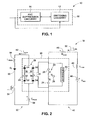
FIG. 1 is a block diagram of an exemplary MEMS based switching system, in accordance with aspects of the present technique; -
FIG. 2 is schematic diagram illustrating the exemplary MEMS based switching system depicted inFIG. 1 ; -
FIGs. 3-5 are schematic flow charts illustrating an example operation of the MEMS based switching system illustrated inFIG. 2 ; -
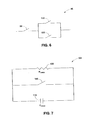
FIG. 6 is schematic diagram illustrating a series-parallel array of MEMS switches; -
FIG. 7 is schematic diagram illustrating a graded MEMS switch; -
FIG. 8 is a flow diagram depicting an operational flow of a system having the MEMS based switching system illustrated inFIG. 1 ; -
FIG. 9 is a graphical representation of experimental results representative of turn off of the switching system. -
FIG. 10 is schematic diagram illustrating an exemplary MEMS-based switching system, in accordance with aspects of the present invention; and -
FIGs. 11 and12 respectively illustrate a graphical representation of simulation results of example circuit signals illustrative of operational details of the switching system ofFIG. 10 , in accordance with aspects of the present invention. - In accordance with one or more embodiments of the present invention, systems and methods for micro-electromechanical system based arc-less switching is described herein. In the following detailed description, numerous specific details are set forth in order to provide a thorough understanding of various embodiments of the present invention. However, those skilled in the art will understand that embodiments of the present invention may be practiced without these specific details, that the present invention is not limited to the depicted embodiments, and that the present invention may be practiced in a variety of alternative embodiments. In other instances, well known methods, procedures, and components have not been described in detail.
- Furthermore, various operations may be described as multiple discrete steps performed in a manner that is helpful for understanding embodiments of the present invention. However, the order of description should not be construed as to imply that these operations need be performed in the order they are presented, nor that they are even order dependent. Moreover, repeated usage of the phrase "in one embodiment" does not necessarily refer to the same embodiment, although it may. Lastly, the terms "comprising", "including", "having", and the like, as used in the present application, are intended to be synonymous unless otherwise indicated.
-
FIG. 1 illustrates a block diagram of an exemplary arc-less micro-electromechanical system switch (MEMS) basedswitching system 10, in accordance with aspects of the present invention. Presently, MEMS generally refer to micron-scale structures that for example can integrate a multiplicity of functionally distinct elements, e.g., mechanical elements, electromechanical elements, sensors, actuators, and electronics, on a common substrate through micro-fabrication technology. It is contemplated, however, that many techniques and structures presently available in MEMS devices will in just a few years be available via nanotechnology-based devices, e.g., structures that may be smaller than 100 nanometers in size. Accordingly, even though example embodiments described throughout this document may refer to MEMS-based switching devices, it is submitted that the inventive aspects of the present invention should be broadly construed and should not be limited to micron-sized devices. - As illustrated in
FIG. 1 , the arc-less MEMS basedswitching system 10 is shown as including MEMS basedswitching circuitry 12 andarc suppression circuitry 14, where thearc suppression circuitry 14 is operatively coupled to the MEMS basedswitching circuitry 12. In certain embodiments, the MEMS basedswitching circuitry 12 may be integrated in its entirety with thearc suppression circuitry 14 in asingle package 16, for example. In other embodiments, only certain portions or components of the MEMS basedswitching circuitry 12 may be integrated with thearc suppression circuitry 14. - In a presently contemplated configuration as will be described in greater detail with reference to
FIGs. 2-5 , the MEMS basedswitching circuitry 12 may include one or more MEMS switches. Additionally, thearc suppression circuitry 14 may include a balanced diode bridge and a pulse circuit. Further, thearc suppression circuitry 14 may be configured to facilitate suppression of an arc formation between contacts of the one or more MEMS switches. It may be noted that thearc suppression circuitry 14 may be configured to facilitate suppression of an arc formation in response to an alternating current (AC) or a direct current (DC). - Turning now to
FIG. 2 , a schematic diagram 18 of the exemplary arc-less MEMS based switching system depicted inFIG. 1 is illustrated in accordance with one embodiment. As noted with reference toFIG. 1 , the MEMS basedswitching circuitry 12 may include one or more MEMS switches. In the illustrated embodiment, afirst MEMS switch 20 is depicted as having afirst contact 22, asecond contact 24 and athird contact 26. In one embodiment, thefirst contact 22 may be configured as a drain, thesecond contact 24 may be configured as a source and thethird contact 26 may be configured as a gate. Furthermore, as illustrated inFIG. 2 , avoltage snubber circuit 33 may be coupled in parallel with theMEMS switch 20 and configured to limit voltage overshoot during fast contact separation as will be explained in greater detail hereinafter. In certain embodiments, thesnubber circuit 33 may include a snubber capacitor (not shown) coupled in series with a snubber resistor (not shown). The snubber capacitor may facilitate improvement in transient voltage sharing during the sequencing of the opening of theMEMS switch 20. Furthermore, the snubber resistor may suppress any pulse of current generated by the snubber capacitor during closing operation of theMEMS switch 20. In certain other embodiments, thevoltage snubber circuit 33 may include a metal oxide varistor (MOV) (not shown). - In accordance with further aspects of the present technique, a
load circuit 40 may be coupled in series with thefirst MEMS switch 20. Theload circuit 40 may include avoltage source V BUS 44. In addition, theload circuit 40 may also include a load inductance 46 LLOAD, where theload inductance L LOAD 46 is representative of a combined load inductance and a bus inductance viewed by theload circuit 40. Theload circuit 40 may also include aload resistance R LOAD 48 representative of a combined load resistance viewed by theload circuit 40.Reference numeral 50 is representative of a load circuit current ILOAD that may flow through theload circuit 40 and thefirst MEMS switch 20. - Further, as noted with reference to
FIG. 1 , thearc suppression circuitry 14 may include a balanced diode bridge. In the illustrated embodiment, abalanced diode bridge 28 is depicted as having afirst branch 29 and asecond branch 31. As used herein, the term "balanced diode bridge" is used to represent a diode bridge that is configured such that voltage drops across both the first andsecond branches first branch 29 of thebalanced diode bridge 28 may include afirst diode D1 30 and asecond diode D2 32 coupled together to form a first series circuit. In a similar fashion, thesecond branch 31 of thebalanced diode bridge 28 may include athird diode D3 34 and afourth diode D4 36 operatively coupled together to form a second series circuit. - In one embodiment, the
first MEMS switch 20 may be coupled in parallel across midpoints of thebalanced diode bridge 28. The midpoints of the balanced diode bridge may include a first midpoint located between the first andsecond diodes fourth diodes first MEMS switch 20 and thebalanced diode bridge 28 may be tightly packaged to facilitate minimization of parasitic inductance caused by thebalanced diode bridge 28 and in particular, the connections to theMEMS switch 20. It may be noted that, in accordance with exemplary aspects of the present technique, thefirst MEMS switch 20 and thebalanced diode bridge 28 are positioned relative to one another such that the inherent inductance between thefirst MEMS switch 20 and thebalanced diode bridge 28 produces a di/dt voltage less than a few percent of the voltage across thedrain 22 andsource 24 of theMEMS switch 20 when carrying a transfer of the load current to thediode bridge 28 during theMEMS switch 20 turn-off which will be described in greater detail hereinafter. In one embodiment, thefirst MEMS switch 20 may be integrated with thebalanced diode bridge 28 in asingle package 38 or optionally, the same die with the intention of minimizing the inductance interconnecting theMEMS switch 20 and thediode bridge 28. - Additionally, the
arc suppression circuitry 14 may include apulse circuit 52 coupled in operative association with thebalanced diode bridge 28. Thepulse circuit 52 may be configured to detect a switch condition and initiate opening of theMEMS switch 20 responsive to the switch condition. As used herein, the term "switch condition" refers to a condition that triggers changing a present operating state of theMEMS switch 20. For example, the switch condition may result in changing a first closed state of theMEMS switch 20 to a second open state or a first open state of theMEMS switch 20 to a second closed state. A switch condition may occur in response to a number of actions including but not limited to a circuit fault or switch ON/OFF request. - The
pulse circuit 52 may include apulse switch 54 and apulse capacitor C PULSE 56 series coupled to thepulse switch 54. Further, the pulse circuit may also include apulse inductance L PULSE 58 and afirst diode D P 60 coupled in series with thepulse switch 54. Thepulse inductance L PULSE 58, thediode D P 60, thepulse switch 54 and thepulse capacitor C PULSE 56 may be coupled in series to form a first branch of thepulse circuit 52, where the components of the first branch may be configured to facilitate pulse current shaping and timing. Also,reference numeral 62 is representative of a pulse circuit current IPULSE that may flow through thepulse circuit 52. - In accordance with aspects of the present invention as will be described in further detail hereinafter, the
MEMS switch 20 may be rapidly switched (e.g., on the order of picoseconds or nanoseconds) from a first closed state to a second open state while carrying a current albeit at a near-zero voltage. This may be achieved through the combined operation of theload circuit 40, andpulse circuit 52 including thebalanced diode bridge 28 coupled in parallel across contacts of theMEMS switch 20. -
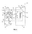
FIGs. 3-5 are used as schematic flow charts to illustrate an example operation of the arc-less MEMS based switchingsystem 18 illustrated inFIG. 2 . With continuing reference toFIG. 2 , an initial condition of the example operation of the arc-less MEMS based switchingsystem 18 is illustrated. TheMEMS switch 20 is depicted as starting in a first closed state. Also, as indicated, there is a load current ILOAD 50 which has a value substantially equal to VBUS /RLOAD in theload circuit 40. - Moreover, for discussion of this example operation of the arc-less MEMS based switching
system 18, it may be assumed that a resistance associated with theMEMS switch 20 is sufficiently small such that the voltage produced by the load current through the resistance ofMEMS switch 20 has only a negligible effect on the near-zero voltage difference between the mid-points of thediode bridge 28 when pulsed. For example, the resistance associated with theMEMS switch 20 may be assumed to be sufficiently small so as to produce a voltage drop of less than a few millivolts due to the maximum anticipated load current. - It may be noted that in this initial condition of the MEMS based switching
system 18, thepulse switch 54 is in a first open state. Additionally, there is no pulse circuit current in thepulse circuit 52. Also, in thepulse circuit 52, thecapacitor C PULSE 56 may be pre-charged to a voltage VPULSE, where VPULSE is a voltage that can produce a half sinusoid of pulse current having a peak magnitude significantly greater (e.g., twice) the anticipated load current ILOAD 50 during the transfer interval of the load current. It may be noted thatC PULSE 56 andL PULSE 58 may be selected so as to resonate with each other. -
FIG. 3 illustrates a schematic diagram 64 depicting a process of triggering thepulse circuit 52. It may be noted that detection circuitry (not shown) may be coupled to thepulse circuit 52. The detection circuitry may include sensing circuitry (not shown) configured to sense a level of the load circuit current ILOAD 50 and/or a voltage level of thevoltage source V BUS 44, for example. Furthermore, the detection circuitry may be configured to detect a switch condition as described above. In one embodiment, the switch condition may occur due to the current level and/or the voltage level exceeding a predetermined threshold. - The
pulse circuit 52 may be configured to detect the switch condition to facilitate switching the present closed state of theMEMS switch 20 to a second open state. In one embodiment, the switch condition may be a fault condition generated due to a voltage level or load current in theload circuit 40 exceeding a predetermined threshold level. However, as will be appreciated, the switch condition may also include monitoring a ramp voltage to achieve a given system-dependent ON time for theMEMS switch 20. - In one embodiment, the
pulse switch 54 may generate a sinusoidal pulse responsive to receiving a trigger signal as a result of a detected switching condition. The triggering of thepulse switch 54 may initiate a resonant sinusoidal current in thepulse circuit 52. The current direction of the pulse circuit current may be represented byreference numerals first diode 30 and thesecond diode 32 of thefirst branch 29 of thebalanced diode bridge 28 may be represented bycurrent vectors current vectors third diode 34 and thefourth diode 36 respectively. - The value of the peak sinusoidal bridge pulse current may be determined by the initial voltage on the
pulse capacitor C PULSE 56, value of thepulse capacitor C PULSE 56 and the value of thepulse inductance L PULSE 58. The values for thepulse inductance L PULSE 58 and thepulse capacitor C PULSE 56 also determine the pulse width of the half sinusoid of pulse current. The bridge current pulse width may be adjusted to meet the system load current turn-off requirement predicated upon the rate of change of the load current (VBUS /LLOAD ) and the desired peak let-through current during a load fault condition. According to aspects of the present invention, thepulse switch 54 may be configured to be in a conducting state prior to opening theMEMS switch 20. - It may be noted that triggering of the
pulse switch 54 may include controlling a timing of the pulse circuit current IPULSE 62 through thebalanced diode bridge 28 to facilitate creating a lower impedance path as compared to the impedance of a path through the contacts of theMEMS switch 20 during an opening interval. In addition, thepulse switch 54 may be triggered such that a desired voltage drop is presented across the contacts of theMEMS switch 20. - In one embodiment, the
pulse switch 54 may be a solid-state switch that may be configured to have switching speeds in the range of nanoseconds to microseconds, for example. The switching speed of thepulse switch 54 should be relatively fast compared to the anticipated rise time of the load current in a fault condition. The current rating of theMEMS switch 20 is dependent on the rate of rise of the load current, which in turn is dependent on theinductance L LOAD 46 and the bussupply voltage V BUS 44 in theload circuit 40 as previously noted. TheMEMS switch 20 may be appropriately rated to handle a larger load current ILOAD 50 if the load current - ILOAD 50 may rise rapidly compared to the speed capability of the bridge pulse circuit.
- The pulse circuit current IPULSE 62 increases from a value of zero and divides equally between the first and
second branches balanced diode bridge 28. In accordance with one embodiment, the difference in voltage drops across thebranches balanced diode bridge 28 may be designed to be negligible, as previously described. Further, as previously described, thediode bridge 28 is balanced such that the voltage drop across the first and second branches of thediode bridge 28 are substantially equal. Moreover, as the resistance of theMEMS switch 20 in a present closed state is relatively low, there is a relatively small voltage drop across theMEMS switch 20. However, if the voltage drop across theMEMS switch 20 happened to be larger (e.g., due to an inherent design of the MEMS switch), the balancing of thediode bridge 28 may be affected as thediode bridge 28 is operatively coupled in parallel with theMEMS switch 20. In accordance with aspects of the present invention, if the resistance of theMEMS switch 20 causes a significant voltage drop across theMEMS switch 20 then thediode bridge 28 may accommodate the resulting imbalance of the pulse bridge by increasing the magnitude of the peak bridge pulse current. - Referring now to
FIG. 4 , a schematic diagram 78 is illustrated in which opening of theMEMS switch 20 is initiated. As previously noted, thepulse switch 54 in thepulse circuit 52 is triggered prior to opening theMEMS switch 20. As the pulse current IPULSE 62 increases, the voltage across thepulse capacitor C PULSE 56 decreases due to the resonant action of thepulse circuit 52. In the ON condition in which the switch is closed and conducting, theMEMS switch 20 presents a path of relatively low impedance for the load circuitcurrent I LOAD 50. - Once the amplitude of the pulse circuit current IPULSE 62 becomes greater than the amplitude of the load circuit current ILOAD 50 (e.g., due to the resonant action of the pulse circuit 52), a voltage applied to the
gate contact 26 of theMEMS switch 20 may be appropriately biased to switch the present operating state of theMEMS switch 20 from the first closed and conducting state to an increasing resistance condition in which theMEMS switch 20 starts to turn off (e.g., where the contacts are still closed but contact pressure diminishing due the switch opening process) which causes the switch resistance to increase which in turn causes the load current to start to divert from theMEMS switch 20 into thediode bridge 28. - In this present condition, the
balanced diode bridge 28 presents a path of relatively low impedance to the load circuit current ILOAD 50 as compared to a path through theMEMS switch 20, which now exhibits an increasing contact resistance. It may be noted that this diversion of load circuit current ILOAD 50 through theMEMS switch 20 is an extremely fast process compared to the rate of change of the load circuitcurrent I LOAD 50. As previously noted, it may be desirable that the values ofinductances L 1 84 andL 2 88 associated with connections between theMEMS switch 20 and thebalanced diode bridge 28 be very small to avoid inhibition of the fast current diversion. - The process of current transfer from the
MEMS switch 20 to the pulse bridge continues to increase the current in thefirst diode 30 and thefourth diode 36 while simultaneously the current in thesecond diode 32 and thethird diode 34 diminish. The transfer process is completed when themechanical contacts MEMS switch 20 are separated to form a physical gap and all of the load current is carried by thefirst diode 30 and thefourth diode 36. - Consequent to the load circuit current ILOAD being diverted from the
MEMS switch 20 to thediode bridge 28 indirection 86, an imbalance forms across the first andsecond branches diode bridge 28. Furthermore, as the pulse circuit current decays, voltage across thepulse capacitor C PULSE 56 continues to reverse (e.g., acting as a "back electro-motive force") which causes the eventual reduction of the load circuit current ILOAD to zero. Thesecond diode 32 and thethird diode 34 in thediode bridge 28 become reverse biased which results in the load circuit now including thepulse inductor L PULSE 58 and the bridgepulse capacitor C PULSE 56 and to become a series resonant circuit. - Turning now to
FIG. 5 , a schematic diagram 94 for the circuit elements connected for the process of decreasing the load current is illustrated. As alluded to above, at the instant that the contacts of theMEMS switch 20 part, infinite contact resistance is achieved. Furthermore, thediode bridge 28 no longer maintains a near-zero voltage across the contacts of theMEMS switch 20. Also, the load circuit current ILOAD is now equal to the current through thefirst diode 30 and thefourth diode 36. As previously noted, there is now no current through thesecond diode 32 and thethird diode 34 of thediode bridge 28. - Additionally, a significant switch contact voltage difference from the
drain 24 to thesource 26 of theMEMS switch 20 may now rise to a maximum of approximately twice the VBUS voltage at a rate determined by the net resonant circuit which includes thepulse inductor L PULSE 58, thepulse capacitor C PULSE 56, the load circuit inductor -
L LOAD 46, and damping due to theload resistor R LOAD 48 and circuit losses. - Moreover, the pulse circuit current IPULSE 62, that is now equal to the load circuit current ILOAD 50, may resonantly decrease to a zero value and to maintain the zero value due to the reverse blocking action of the
diode bridge 28 and thediode D P 60. - The voltage across the
pulse capacitor C PULSE 56 has reversed resonantly to a negative peak and will maintain the negative peak value until thepulse capacitor C PULSE 56 is recharged. - The
diode bridge 28 may be configured to maintain a near-zero voltage across the contacts of theMEMS switch 20 until the contacts separate to open theMEMS switch 20, thereby preventing damage by suppressing any arc that would tend to form between the contacts of theMEMS switch 20 during opening. Additionally, the contacts of theMEMS switch 20 approach the opened state at a much reduced contact current through theMEMS switch 20. Also, any stored energy in the circuit inductance, the load inductance and the source may be transferred to the pulsecircuit capacitor C PULSE 56 and may be absorbed via voltage dissipation circuitry (not shown). Thevoltage snubber circuit 33 may be configured to limit voltage overshoot during the fast contact separation due to the inductive energy remaining in the interface inductance between the bridge and the MEMS switch. Furthermore, the rate of increase of reapply voltage across the contacts of theMEMS switch 20 during opening may be controlled via use of the snubber circuit (not shown). - It may also be noted that although a gap is created between the contacts of the
MEMS switch 20 when in an open state, a leakage current may nonetheless exist between theload circuit 40 and thediode bridge circuit 28 around theMEMS switch 20. This leakage current may be suppressed via introduction of a secondary mechanical switch (not shown) series connected in theload circuit 40 to generate a physical gap. In certain embodiments, the mechanical switch may include a second MEMS switch. -
FIG. 6 illustrates anexemplary embodiment 96 wherein the switching circuitry 12 (seeFIG. 1 ) may include multiple MEMS switches arranged in a series or series-parallel array, for example. Additionally, as illustrated inFIG. 6 , theMEMS switch 20 may replaced by a first set of two or more MEMS switches 98, 100 electrically coupled in a series circuit. In one embodiment, at least one of the first set of MEMS switches 98, 100 may be further coupled in a parallel circuit, where the parallel circuit may include a second set of two or more MEMS switches (e.g.,reference numerals 100, 102). In accordance with aspects of the present invention, a static grading resistor and a dynamic grading capacitor may be coupled in parallel with at least one of the first or second set of MEMS switches. - Referring now to
FIG. 7 , anexemplary embodiment 104 of a graded MEMS switch circuit is depicted. The gradedswitch circuit 104 may include at least oneMEMS switch 106, agrading resistor 108, and agrading capacitor 110. The gradedswitch circuit 104 may include multiple MEMS switches arranged in a series or series-parallel array as for example illustrated inFIG. 6 . Thegrading resistor 108 may be coupled in parallel with at least oneMEMS switch 106 to provide voltage grading for the switch array. In an exemplary embodiment, thegrading resistor 108 may be sized to provide adequate steady state voltage balancing (division) among the series switches while providing acceptable leakage for the particular application. Furthermore, both thegrading capacitor 110 andgrading resistor 108 may be provided in parallel with eachMEMS switch 106 of the array to provide sharing both dynamically during switching and statically in the OFF state. It may be noted that additional grading resistors or grading capacitors or both may be added to each MEMS switch in the switch array. -
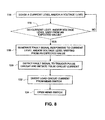
FIG. 8 is a flow chart of exemplary logic 112 for switching a MEMS based switching system from a present operating state to a second state. In accordance with exemplary aspects of the present technique, a method for switching is presented. As previously noted, detection circuitry may be operatively coupled to the arc suppression circuitry and configured to detect a switch condition. In addition, the detection circuitry may include sensing circuitry configured to sense a current level and/or a voltage level. - As indicated by
block 114, a current level in a load circuit, such as the load circuit 40 (seeFIG. 2 ), and/or a voltage level may be sensed, via the sensing circuitry, for example. Additionally, as indicated by decision block 116 a determination may be made as to whether either the sensed current level or the sensed voltage level varies from or exceeds an expected value. In one embodiment, a determination may be made (via the detection circuitry, for example) as to whether the sensed current level or the sensed voltage level exceeds respective predetermined threshold levels. Alternatively, voltage or current ramp rates may be monitored to detect a switch condition without a fault having actually occurred. - If the sensed current level or sensed voltage level varies or departs from an expected value, a switch condition may be generated as indicated by
block 118. As previously noted, the term "switch condition" refers to a condition that triggers changing a present operating state of the MEMS switch. In certain embodiments, the switch condition may be generated responsive to a fault signal and may be employed to facilitate initiating opening of the MEMS switch. It may be noted that blocks 114-118 are representative of one example of generating a switch condition. However as will be appreciated, other methods of generating the switch condition are also envisioned in accordance with aspects of the present invention. - As indicated by
block 120, the pulse circuit may be triggered to initiate a pulse circuit current responsive to the switch condition. Due to the resonant action of the pulse circuit, the pulse circuit current level may continue to increase. Due at least in part to thediode bridge 28, a near-zero voltage drop may be maintained across the contacts of the MEMS switch if the instantaneous amplitude of the pulse circuit current is significantly greater than the instantaneous amplitude of the load circuit current. - Additionally, the load circuit current through the MEMS switch may be diverted from the MEMS switch to the pulse circuit as indicated by
block 122. As previously noted, the diode bridge presents a path of relatively low impedance as opposed to a path through the MEMS switch, where a relatively high impedance increases as the contacts of the MEMS switch start to part. The MEMS switch may then be opened in an arc-less manner as indicated byblock 124. - As previously described, a near-zero voltage drop across contacts of the MEMS switch may be maintained as long as the instantaneous amplitude of the pulse circuit current is significantly greater than the instantaneous amplitude of the load circuit current, thereby facilitating opening of the MEMS switch and suppressing formation of any arc across the contacts of the MEMS switch. Thus, as described hereinabove, the MEMS switch may be opened at a near-zero voltage condition across the contacts of the MEMS switch and with a greatly reduced current through the MEMS switch.
-
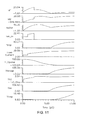
FIG. 9 is agraphical representation 130 of experimental results representative of switching a present operating state of the MEMS switch of the MEMS based switching system, in accordance with aspects of the present technique. As depicted inFIG. 9 , a variation inamplitude 132 is plotted against a variation intime 134. Also,reference numerals graphical illustration 130. -
Response curve 142 represents a variation of amplitude of the load circuit current as a function of time. A variation of amplitude of the pulse circuit current as a function of time is represented inresponse curve 144. In a similar fashion, a variation of amplitude of gate voltage as a function of time is embodied inresponse curve 146.Response curve 148 represents a zero gate voltage reference, whileresponse curve 150 is the reference level for the load current prior to turn-off. - Additionally,
reference numeral 152 represents region on theresponse curve 142 where the process of switch opening occurs. Similarly,reference numeral 154 represents a region on theresponse curve 142 where the contacts of the MEMS switch have parted and the switch is in an open state. Also, as can be seen from thesecond section 138 of thegraphical representation 130, the gate voltage is pulled low to facilitate initiating opening of the MEMS switch. Furthermore, as can be seen from thethird section 140 of thegraphical representation 130, the load circuit current 142 and the pulse circuit current 144 in the conducting half of the balanced diode bridge are decaying. - Additional aspects of the present invention comprise the addition of an energy-absorbing
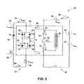
circuitry 200, shown inFIG. 10 , adapted to absorb (e.g., trap or take up) electrical energy during a switched load current interruption of a protected load circuit, such as may occur in response to a fault condition. This circuitry is connected in a parallel circuit withbalanced diode bridge 28. It is contemplated that this addition will enable optimization of load current interruption due to fault conditions that may develop in the load circuit and will be conducive to a decreased amount of let-through current in switching circuitry embodying aspects of the present invention. Moreover, aspects of the present invention should simplify the circuit design process, and should further enable optimization of circuitry components in a MEMS-based switching system, such as enabling appropriate circuitry selection for a given application, and reduced weight and cost of the switching system. - In one example embodiment, energy-absorbing
circuitry 200 is connected across the DC side ofbalanced diode bridge 28 in parallel withpulse circuit 52 as shown inFIG. 10 .Circuitry 200 may comprise a resistor Rt, a diode Dt, and an energy-absorbing element, such as a capacitor Ct. For purposes of description of operational interactions effected bycircuitry 200, let us begin upon the opening ofMEMS switch 20 to a non-conductive state, and upon a turning off of the two mutually diagonal bridge diodes (e.g.,diodes 32 and 34) that may be shedding current during the process for limiting fault current. The diode bridge voltage will rapidly rise above an initial voltage value (VtIni) stored on capacitor Ct and diode Dt will then turn on. It will be appreciated that electrical energy, which is stored in capacitor Ct upon occurrence of a fault, may be readily discharged by way of a suitable discharge resistor (not shown inFIG. 10 ). - The inventors of the present invention have innovatively recognized structural and/or operational relationships that permit independent optimization of
pulse circuit 52 and energy-absorbingcircuitry 200 for a given circuit breaker application. This optimization can result in an appropriate selection of components and/or substantial cost reductions for a given application. For example, the value of pulse capacitor Cp and its initial voltage (VpIni) may be advantageously selected (e.g., selecting a sufficiently small capacitance value for capacitor Cp) to achieve an optimum peak pulse current and/or pulse width independent of energy-absorbing capacitor Ct. That is, independent of energy trapping requirements that otherwise would have to be carried out by way of pulse capacitor Cpulse in addition to the pulse-forming requirements. Similarly, the value of energy-absorbing capacitor Ct and its initial voltage (Vtlni) can be independently selected (e.g., selecting a sufficiently large capacitance value for energy-absorbing capacitor Ct) for rapid absorption of the fault energy during a fault interval. That is, independent of the pulse-forming requirements carried out by way of capacitor Cp. - A circuit arrangement embodying aspects of the present invention should result in a reduced amount of fault let-through current and lower breaker energy dissipation. As noted above,
diode bridge 28 and MEMS switch 20 may be packaged to be closely integrated with one another (e.g., composite packaging) for reduction of parasitic inductance in the diode bridge and the respective interconnections to the MEMS switch. This incrementally reduces the amount of electrical energy that may be stored in such interconnections. Otherwise, during the opening of the MEMS switch, a corresponding incremental amount of electrical energy would have to be dissipated by the opening contacts of the MEMS switch since the additional inductance of the interconnections tosnubber 33 would diminish effecting protective action by the protective circuitry (e.g., snubber 33) connected acrossMEMS switch 20 at the instant the contacts disengage. It is noted that one important function ofsnubber 33 is to retard (e.g., slow down) the rise of the voltage across the MEMS switch during the opening motion of the contacts to prevent arcing due to excessive voltage gradient buildup until full separation and voltage hold-off capability has been achieved. - In operation, (in response to a fault that can develop in the load circuit) reliable and substantially rapid turn-off of the load current may be accomplished through the following example sequence of events, as may be performed in a MEMS-based switching system embodying aspects of the present invention: Capacitors Cpulse and Ct may be respectively initially charged with the respective example voltage polarities shown in
FIG. 10 to initial voltages VpInit and VtInit.MEMS switch 20 initially will be in an ON (e.g., conductive) state in response to a gating signal applied viacontact gate 26. Upon occurrence of a fault, load current will rise at a relatively fast rate (e.g., high value of di/dt). For example, when the magnitude of the load current exceeds a predefined threshold value and/or the rate of change (di/dt) of the load current exceeds a predefined value,pulse switch 54 is triggered to an ON state. The value of Ipulse current will then increase to a suitable preset (design) value that exceeds the fault current value. As previously discussed, thepulsed diode bridge 28 is configured to cause a nearly zero voltage drop acrossMEMS switch 20. At a time just prior to reaching the peak value of Ipulse current,MEMS switch 20 will be gated to an OFF (non-conductive) state. - As the MEMS switch contact pressure decreases in response to a decreasing gating signal, the increasing contact resistance forces a current transfer from the load circuit to the
diode bridge 28. Current flow throughswitch contacts Contacts diode bridge 28. The value of Ipulse current will decrease (e.g., in a sinusoidal manner) after reaching its peak value. When the value of Ipulse current decreases to a value that matches the instantaneous value of the increasing fault current, diodes D2 and D3 will cease to conduct. At this point, diodes D1 and D4 will conduct the fault current from the load circuit. Also pulse capacitor Cpulse decreases in voltage until its voltage polarity reverses. The increase in the magnitude of the reverse voltage being stored on capacitor Cpulse by the fault current will opposebus source voltage 44 and will cause a decrease in the rise rate of fault current, di/dt. - The voltage across the DC input to
diode bridge 28 will then increase rapidly and when its value reaches the initial voltage (VtInit) stored on capacitor Ct, diode Dt will begin to conduct andcircuitry 200 will take up the fault current. Capacitor Ct, as it is being charged, creates a reverse emf which reverses the rise rate of fault current (e.g., negative di/dt). For instance, when the voltage on capacitor Ct reaches the bus source voltage, then the fault current will decrease to zero. From the foregoing description, it will be appreciated that energy-absorbing capacitor Ct is adapted to absorb fault-resulting electrical energy independent of the pulse circuit, and to cause the extremely rapid reduction of load current to zero through its resonant action with the load and pulse inductances. - It will be appreciated that a circuit arrangement embodying aspects of the present invention advantageously separates the functions provided by capacitors Ct and Cpulse. Furthermore, the circuit branch with the energy-absorbing capacitor Ct may be conceptualized to function as a "snubber" in the sense of controlling (e.g., restraining) the rate-of-change (e.g., rate-of-rise) of the voltage across the diode bridge as well as absorbing the load/source system energy. This may be achieved in one example embodiment with an adjustable pre-charge on capacitor Ct.
-
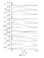
FIG. 11 synthesizes in graphical form the operational concepts discussed above through simulated circuit signals plotted as a function of time for the MEMS-based switching system shown inFIG. 10 . These signals are plotted over an example time interval of 10 microseconds (as may be useful for appreciating operational details regarding an example initial transient response of the switching system) during a switched turn-off of the load current in response to a fault condition whileFIG. 12 shows such simulated circuit signals plotted over a longer time interval, such as 120 microseconds, (as may be useful for appreciating operational details over that longer time interval and regarding an example response of the switching system subsequent to turn-off of the load current). - The signal plots in
FIGs. 11 and12 are identified as follows in reference to the system shown inFIG. 10 :Id 1 and Id2 represent currents respectively conducted by bridge diodes D1 and D2. Ipulse represents pulse current. Isw_in represents current flow throughcontacts MEMS switch 20. Itrap represents current flow through energy-absorbingcircuitry 200. Load Current represents a load current in response to a fault condition, as such current is effectively limited by the system shown inFIG. 10 . V_Cpulse represents a voltage acrosspulse capacitor 56. Vbridge represents a voltage acrossdiode bridge 28. Vd2 represents a voltage across diode D2. Vsw represents a voltage acrosscontacts MEMS switch 20. Vtrap represents a voltage across energy-absorbing capacitor Ct. - While only certain features of the invention have been illustrated and described herein, many modifications and changes will occur to those skilled in the art. It is, therefore, to be understood that the appended claims are intended to cover all such modifications and changes as fall within the true spirit of the invention.
-
- 10
- arc-less micro-electromechanical system switch (MEMS) based switching system
- 12
- MEMS based switching circuitry
- 14
- arc suppression circuitry
- 16
- single package
- 18
- schematic diagram of arc-less micro-electromechanical system switch (MEMS) based switching system
- 20
- MEMS switch
- 22
- first contact
- 24
- second contact
- 26
- third contact
- 28
- balanced diode bridge
- 29
- first branch of balanced diode bridge
- 30
- first diode D1
- 31
- second branch of balanced diode bridge
- 32
- second diode
- 33
- voltage snubber circuit
- 34
- third diode D3
- 36
- fourth diode D4
- 38
- single package
- 40
- a load circuit
- 44
- voltage source VBUS
- 46
- load inductance
- 48
- load resistance RLOAD
- 50
- load circuit current
- 52
- pulse circuit
- 54
- pulse switch
- 56
- pulse capacitor CPULSE
- 58
- pulse inductance LPULSE
- 60
- first diode DP
- 62
- pulse circuit current IPULSE
- 64
- schematic diagram of process for trigering pulse circuit
- 66, 68
- direction of pulse circuit current
- 70, 72
- current vectors
- 74, 76
- current vectors
- 78
- schematic diagram indicating initiation of opening of MEMS switch
- 84, 88
- inductances
- 86
- load current direction
- 94
- schematic diagram of circuit elements
- 96
- exemplary embodiment of switching circuitry
- 98, 100, 102
- MEMS switches
- 104
- graded switch circuit
- 106
- MEMS switch
- 108
- grading resistor
- 110
- grading capacitor
- 112
- flow chart of exemplary logic
- 114
- sensing block
- 116
- decision block
- 118
- generating of switch condition block
- 120
- triggering block
- 122
- current diverting block
- 124
- arcless opening block
- 130
- graphical representation of experimentasl results
- 132
- variation in amplitude
- 134
- variation in time
- 136, 138,140
- reference numerals representative of first, second and third sections of
graphical representation 130 - 142
- response curve
- 144
- response curve
- 146
- response curve
- 148
- response curve
- 152
- region of
response curve 142 indicating process of switch opening. - 154
- region of
response curve 142 indicating open state of switch - 200
- energy-absorbing circuitry
Claims (11)
- A system (10), comprising:a micro-electromechanical system switch (20);a balanced diode bridge (28) configured to suppress arc formation between contacts of the micro-electromechanical system switch;a pulse circuit (52) coupled to the balanced diode bridge, the pulse circuit comprising a pulse capacitor adapted to form a pulse signal for causing flow of a pulse current through the balanced diode bridge, the pulse signal being generated in response to a fault condition in a load circuit coupled to the micro-electromechanical system switch; andenergy-absorbing circuitry (200) coupled in a parallel circuit with the pulse circuit, the circuitry comprising an energy-absorbing capacitor (Ct) adapted to absorb electrical energy resulting from the fault condition without affecting a pulse signal formation by the pulse circuit, wherein the energy-absorbing capacitor is further adapted for restraining a rate-of-change of a voltage that develops across the diode bridge upon occurrence of the fault condition.
- The system (10) of claim 1 wherein a capacitance value of the pulse capacitor is selected to control one or more pulse signal characteristics of the pulse signal independent of a capacitance value of the energy-absorbing capacitor.
- The system (10) of claim 2 wherein the one or more pulse signal characteristics of the pulse signal are selected from the group consisting of a width of the pulse signal, a peak of the pulse signal, and a combination thereof.
- The system (10) of any preceding claim wherein a capacitance value of the energy-absorbing capacitor (Ct) is selected to control an amount of electrical energy absorbed by the energy-absorbing capacitor independent of a capacitance value of the pulse capacitor.
- The system (10) of any preceding claim wherein the energy-absorbing circuitry (200) further comprises a diode (Dt) connected in a series circuit with the energy-absorbing capacitor (Ct), said diode being connected to be in a conductive state when the voltage that develops across the diode bridge reaches a value that matches a value of an initial voltage value stored in the energy absorbing capacitor, wherein the conductive state of said diode causes the energy-absorbing circuitry to receive fault current.
- The system (10) of any preceding claim, wherein the balanced diode bridge comprises a first branch and a second branch, and wherein the first branch comprises a first diode and a second diode coupled in a first series circuit and the second branch comprises a third diode and a fourth diode coupled in a second series circuit.
- The system (10) of claim 6, wherein the micro-electromechanical system switch is coupled in parallel across midpoints of the balanced diode bridge, and wherein a first midpoint is located between the first and second diodes and a second midpoint is located between the third and fourth diodes.
- The system (10) of any preceding claim, wherein the micro-electromechanical system switch is integrated with the balanced diode bridge in a single package.
- The system (10) of any preceding claim, wherein the pulse circuit (52) is further configured to detect a fault condition and initiate opening of the micro-electromechanical system switch responsive to the fault condition.
- The system (10) of any preceding claim, further comprising a first plurality of micro-electromechanical switches electrically coupled in a series circuit.
- The system (10) of claim 10, wherein at least one of the first plurality of micro-electromechanical switches is further coupled in a parallel circuit comprising a second plurality of micro-electromechanical switches.
Applications Claiming Priority (1)
| Application Number | Priority Date | Filing Date | Title |
|---|---|---|---|
| US11/563,726 US7876538B2 (en) | 2005-12-20 | 2006-11-28 | Micro-electromechanical system based arc-less switching with circuitry for absorbing electrical energy during a fault condition |
Publications (3)
| Publication Number | Publication Date |
|---|---|
| EP1928005A2 true EP1928005A2 (en) | 2008-06-04 |
| EP1928005A3 EP1928005A3 (en) | 2009-07-15 |
| EP1928005B1 EP1928005B1 (en) | 2013-09-25 |
Family
ID=39083243
Family Applications (1)
| Application Number | Title | Priority Date | Filing Date |
|---|---|---|---|
| EP07110553.0A Active EP1928005B1 (en) | 2006-11-28 | 2007-06-19 | Micro-electromechanical system based arc-less switching with circuity for absorbing electrical energy during a fault condition |
Country Status (5)
| Country | Link |
|---|---|
| US (2) | US7876538B2 (en) |
| EP (1) | EP1928005B1 (en) |
| JP (1) | JP5202882B2 (en) |
| CN (1) | CN101192477B (en) |
| MX (1) | MX2007014897A (en) |
Cited By (1)
| Publication number | Priority date | Publication date | Assignee | Title |
|---|---|---|---|---|
| US9087653B2 (en) | 2010-03-12 | 2015-07-21 | Arc Suppression Technologies, Llc | Two terminal arc suppressor |
Families Citing this family (20)
| Publication number | Priority date | Publication date | Assignee | Title |
|---|---|---|---|---|
| US7876538B2 (en) * | 2005-12-20 | 2011-01-25 | General Electric Company | Micro-electromechanical system based arc-less switching with circuitry for absorbing electrical energy during a fault condition |
| US9076607B2 (en) * | 2007-01-10 | 2015-07-07 | General Electric Company | System with circuitry for suppressing arc formation in micro-electromechanical system based switch |
| US7542250B2 (en) * | 2007-01-10 | 2009-06-02 | General Electric Company | Micro-electromechanical system based electric motor starter |
| US8358488B2 (en) * | 2007-06-15 | 2013-01-22 | General Electric Company | Micro-electromechanical system based switching |
| US7554222B2 (en) * | 2007-11-01 | 2009-06-30 | General Electric Company | Micro-electromechanical system based switching |
| IL194955A0 (en) * | 2008-10-28 | 2009-08-03 | Alexsander Ulanovsky | Solid state device for voltage decreasing for the electric circuit of direct and alternating current of medium and high voltage |
| US8427792B2 (en) * | 2009-05-29 | 2013-04-23 | General Electric Company | Method and system to enhance reliability of switch array |
| US8203319B2 (en) * | 2009-07-09 | 2012-06-19 | General Electric Company | Transformer on-load tap changer using MEMS technology |
| US8916995B2 (en) * | 2009-12-02 | 2014-12-23 | General Electric Company | Method and apparatus for switching electrical power |
| JP2012238586A (en) * | 2011-04-28 | 2012-12-06 | General Electric Co <Ge> | Switching array having circuitry to adjust temporal distribution of applied gating signal |
| US20130027817A1 (en) * | 2011-07-25 | 2013-01-31 | General Electric Company | Micro electro-mechanical switch (mems) based over current motor protection system |
| US8773235B2 (en) | 2011-11-30 | 2014-07-08 | General Electric Company | Electrical switch and circuit breaker |
| US20140091808A1 (en) * | 2012-09-28 | 2014-04-03 | Arc Suppression Technologies | Contact separation detector and methods therefor |
| US8659326B1 (en) | 2012-09-28 | 2014-02-25 | General Electric Company | Switching apparatus including gating circuitry for actuating micro-electromechanical system (MEMS) switches |
| US10083811B2 (en) * | 2015-10-22 | 2018-09-25 | General Electric Company | Auxiliary circuit for micro-electromechanical system relay circuit |
| US10068733B2 (en) | 2015-10-22 | 2018-09-04 | General Electric Company | Micro-electromechanical system relay circuit |
| US10211622B2 (en) | 2016-06-29 | 2019-02-19 | General Electric Company | System and method for fault interruption with MEMS switches |
| JP6611989B2 (en) * | 2017-04-18 | 2019-11-27 | 三菱電機株式会社 | Overcurrent detection circuit and power conversion device |
| GB2569185A (en) | 2017-12-11 | 2019-06-12 | Eaton Intelligent Power Ltd | Fault clearing circuitry |
| US11114257B2 (en) * | 2018-04-06 | 2021-09-07 | Yazaki North America, Inc. | Methods and apparatus for DC arc detection/suppression |
Family Cites Families (16)
| Publication number | Priority date | Publication date | Assignee | Title |
|---|---|---|---|---|
| US4500934A (en) | 1982-06-21 | 1985-02-19 | General Electric Company | Hybrid switching device employing liquid metal contact |
| US4700256A (en) | 1984-05-16 | 1987-10-13 | General Electric Company | Solid state current limiting circuit interrupter |
| JPS61259416A (en) * | 1985-05-10 | 1986-11-17 | 大光電気株式会社 | Switching circuit |
| US4723187A (en) | 1986-11-10 | 1988-02-02 | General Electric Company | Current commutation circuit |
| DE3688469T2 (en) | 1986-12-22 | 1993-10-28 | Acec Transport Sa | Ultra-fast switch supported by semiconductors. |
| US5339210A (en) * | 1992-07-22 | 1994-08-16 | General Electric Company | DC circuit interrupter |
| US5430597A (en) | 1993-01-04 | 1995-07-04 | General Electric Company | Current interrupting device using micromechanical components |
| US5374792A (en) * | 1993-01-04 | 1994-12-20 | General Electric Company | Micromechanical moving structures including multiple contact switching system |
| DE19846639A1 (en) | 1998-10-09 | 2000-04-27 | Abb Research Ltd | Electrical switching device for protective switchgear has micro-relay cells connected in series and parallel, and integrated in chip |
| SE9900852D0 (en) | 1999-03-08 | 1999-03-08 | Secheron Sa | An electrical coil module, an electrical coil comprising such modules, an actuation mechanism including such a coil and a circuit breaker comprising such an actuation mechanism |
| DE19927762A1 (en) | 1999-06-17 | 2001-01-04 | Abb Research Ltd | New electrical switching device for overcurrent protection |
| US6952335B2 (en) | 2002-03-22 | 2005-10-04 | Virginia Tech Intellectual Properties, Inc. | Solid-state DC circuit breaker |
| GB2387480B (en) | 2002-04-09 | 2005-04-13 | Microsaic Systems Ltd | Micro-engineered self-releasing switch |
| EP1538645B1 (en) | 2003-12-05 | 2006-03-01 | Société Technique pour l'Energie Atomique TECHNICATOME | Hybrid circuit breaker |
| US6884950B1 (en) * | 2004-09-15 | 2005-04-26 | Agilent Technologies, Inc. | MEMs switching system |
| US7876538B2 (en) * | 2005-12-20 | 2011-01-25 | General Electric Company | Micro-electromechanical system based arc-less switching with circuitry for absorbing electrical energy during a fault condition |
-
2006
- 2006-11-28 US US11/563,726 patent/US7876538B2/en active Active
-
2007
- 2007-06-19 EP EP07110553.0A patent/EP1928005B1/en active Active
- 2007-06-25 JP JP2007165724A patent/JP5202882B2/en active Active
- 2007-07-02 CN CN2007101273307A patent/CN101192477B/en not_active Expired - Fee Related
- 2007-11-27 MX MX2007014897A patent/MX2007014897A/en active IP Right Grant
-
2010
- 2010-12-14 US US12/967,526 patent/US8050000B2/en active Active
Non-Patent Citations (1)
| Title |
|---|
| None |
Cited By (6)
| Publication number | Priority date | Publication date | Assignee | Title |
|---|---|---|---|---|
| US9087653B2 (en) | 2010-03-12 | 2015-07-21 | Arc Suppression Technologies, Llc | Two terminal arc suppressor |
| US9508501B2 (en) | 2010-03-12 | 2016-11-29 | Arc Suppression Technologies, Llc | Two terminal arc suppressor |
| US10134536B2 (en) | 2010-03-12 | 2018-11-20 | Arc Suppression Technologies, Llc | Two terminal arc suppressor |
| US10748719B2 (en) | 2010-03-12 | 2020-08-18 | Arc Suppression Technologies, Llc | Two terminal arc suppressor |
| US11295906B2 (en) | 2010-03-12 | 2022-04-05 | Arc Suppression Technologies, Llc | Two terminal arc suppressor |
| US11676777B2 (en) | 2010-03-12 | 2023-06-13 | Arc Suppression Technologies, Llc | Two terminal arc suppressor |
Also Published As
| Publication number | Publication date |
|---|---|
| US20110096444A1 (en) | 2011-04-28 |
| US7876538B2 (en) | 2011-01-25 |
| US20070139831A1 (en) | 2007-06-21 |
| CN101192477B (en) | 2012-10-10 |
| EP1928005A3 (en) | 2009-07-15 |
| US8050000B2 (en) | 2011-11-01 |
| JP2008211755A (en) | 2008-09-11 |
| JP5202882B2 (en) | 2013-06-05 |
| CN101192477A (en) | 2008-06-04 |
| MX2007014897A (en) | 2009-02-19 |
| EP1928005B1 (en) | 2013-09-25 |
Similar Documents
| Publication | Publication Date | Title |
|---|---|---|
| EP1928005B1 (en) | Micro-electromechanical system based arc-less switching with circuity for absorbing electrical energy during a fault condition | |
| EP1930922B1 (en) | Electromechanical switching circuitry in parallel with solid state switching circuitry selectively switchable to carry a load current appropriate to such circuitry | |
| US7542250B2 (en) | Micro-electromechanical system based electric motor starter | |
| US8054589B2 (en) | Switch structure and associated circuit | |
| KR101468743B1 (en) | System with circuitry for suppressing arc formation in micro-electromechanical system based switch | |
| US8358488B2 (en) | Micro-electromechanical system based switching | |
| US20070139829A1 (en) | Micro-electromechanical system based arc-less switching | |
| US7633725B2 (en) | Micro-electromechanical system based soft switching | |
| EP2056325B1 (en) | System and method for avoiding contact stiction in micro-electromechanical system based switch | |
| KR101445386B1 (en) | Micro-electromechanical system based arc-less switching with circuitry for absorbing electrical energy during a fault condition | |
| EP2017870B1 (en) | Micro-electromechanical system based soft switching |
Legal Events
| Date | Code | Title | Description |
|---|---|---|---|
| PUAI | Public reference made under article 153(3) epc to a published international application that has entered the european phase |
Free format text: ORIGINAL CODE: 0009012 |
|
| AK | Designated contracting states |
Kind code of ref document: A2 Designated state(s): AT BE BG CH CY CZ DE DK EE ES FI FR GB GR HU IE IS IT LI LT LU LV MC MT NL PL PT RO SE SI SK TR |
|
| AX | Request for extension of the european patent |
Extension state: AL BA HR MK RS |
|
| PUAL | Search report despatched |
Free format text: ORIGINAL CODE: 0009013 |
|
| AK | Designated contracting states |
Kind code of ref document: A3 Designated state(s): AT BE BG CH CY CZ DE DK EE ES FI FR GB GR HU IE IS IT LI LT LU LV MC MT NL PL PT RO SE SI SK TR |
|
| AX | Request for extension of the european patent |
Extension state: AL BA HR MK RS |
|
| 17P | Request for examination filed |
Effective date: 20100115 |
|
| AKX | Designation fees paid |
Designated state(s): DE FR GB IT |
|
| 17Q | First examination report despatched |
Effective date: 20100315 |
|
| GRAP | Despatch of communication of intention to grant a patent |
Free format text: ORIGINAL CODE: EPIDOSNIGR1 |
|
| INTG | Intention to grant announced |
Effective date: 20130425 |
|
| GRAS | Grant fee paid |
Free format text: ORIGINAL CODE: EPIDOSNIGR3 |
|
| GRAA | (expected) grant |
Free format text: ORIGINAL CODE: 0009210 |
|
| AK | Designated contracting states |
Kind code of ref document: B1 Designated state(s): DE FR GB IT |
|
| REG | Reference to a national code |
Ref country code: GB Ref legal event code: FG4D |
|
| REG | Reference to a national code |
Ref country code: DE Ref legal event code: R096 Ref document number: 602007033006 Country of ref document: DE Effective date: 20131121 |
|
| REG | Reference to a national code |
Ref country code: DE Ref legal event code: R097 Ref document number: 602007033006 Country of ref document: DE |
|
| PLBE | No opposition filed within time limit |
Free format text: ORIGINAL CODE: 0009261 |
|
| STAA | Information on the status of an ep patent application or granted ep patent |
Free format text: STATUS: NO OPPOSITION FILED WITHIN TIME LIMIT |
|
| 26N | No opposition filed |
Effective date: 20140626 |
|
| REG | Reference to a national code |
Ref country code: DE Ref legal event code: R097 Ref document number: 602007033006 Country of ref document: DE Effective date: 20140626 |
|
| REG | Reference to a national code |
Ref country code: DE Ref legal event code: R119 Ref document number: 602007033006 Country of ref document: DE |
|
| GBPC | Gb: european patent ceased through non-payment of renewal fee |
Effective date: 20140619 |
|
| REG | Reference to a national code |
Ref country code: DE Ref legal event code: R119 Ref document number: 602007033006 Country of ref document: DE Effective date: 20150101 |
|
| PG25 | Lapsed in a contracting state [announced via postgrant information from national office to epo] |
Ref country code: DE Free format text: LAPSE BECAUSE OF NON-PAYMENT OF DUE FEES Effective date: 20150101 Ref country code: IT Free format text: LAPSE BECAUSE OF NON-PAYMENT OF DUE FEES Effective date: 20140619 |
|
| PG25 | Lapsed in a contracting state [announced via postgrant information from national office to epo] |
Ref country code: GB Free format text: LAPSE BECAUSE OF NON-PAYMENT OF DUE FEES Effective date: 20140619 |
|
| REG | Reference to a national code |
Ref country code: FR Ref legal event code: PLFP Year of fee payment: 10 |
|
| REG | Reference to a national code |
Ref country code: FR Ref legal event code: PLFP Year of fee payment: 11 |
|
| REG | Reference to a national code |
Ref country code: FR Ref legal event code: PLFP Year of fee payment: 12 |
|
| PGFP | Annual fee paid to national office [announced via postgrant information from national office to epo] |
Ref country code: FR Payment date: 20230523 Year of fee payment: 17 |