EP1703532A1 - Micro electromechanical switch and method of manufacturing the same - Google Patents
Micro electromechanical switch and method of manufacturing the same Download PDFInfo
- Publication number
- EP1703532A1 EP1703532A1 EP06111126A EP06111126A EP1703532A1 EP 1703532 A1 EP1703532 A1 EP 1703532A1 EP 06111126 A EP06111126 A EP 06111126A EP 06111126 A EP06111126 A EP 06111126A EP 1703532 A1 EP1703532 A1 EP 1703532A1
- Authority
- EP
- European Patent Office
- Prior art keywords
- movable electrode
- beam portion
- electrode
- movable
- micro electromechanical
- Prior art date
- Legal status (The legal status is an assumption and is not a legal conclusion. Google has not performed a legal analysis and makes no representation as to the accuracy of the status listed.)
- Granted
Links
- 238000004519 manufacturing process Methods 0.000 title claims description 44
- 238000006073 displacement reaction Methods 0.000 claims description 31
- 238000005530 etching Methods 0.000 claims description 29
- 238000000034 method Methods 0.000 claims description 21
- 239000002184 metal Substances 0.000 claims description 20
- 229910052751 metal Inorganic materials 0.000 claims description 20
- 239000000463 material Substances 0.000 claims description 14
- XUIMIQQOPSSXEZ-UHFFFAOYSA-N Silicon Chemical compound [Si] XUIMIQQOPSSXEZ-UHFFFAOYSA-N 0.000 claims description 12
- 229910052710 silicon Inorganic materials 0.000 claims description 12
- 239000010703 silicon Substances 0.000 claims description 12
- 238000000926 separation method Methods 0.000 abstract description 5
- 239000002585 base Substances 0.000 description 61
- VYPSYNLAJGMNEJ-UHFFFAOYSA-N Silicium dioxide Chemical compound O=[Si]=O VYPSYNLAJGMNEJ-UHFFFAOYSA-N 0.000 description 36
- 229910052814 silicon oxide Inorganic materials 0.000 description 36
- WGTYBPLFGIVFAS-UHFFFAOYSA-M tetramethylammonium hydroxide Chemical compound [OH-].C[N+](C)(C)C WGTYBPLFGIVFAS-UHFFFAOYSA-M 0.000 description 26
- 239000000203 mixture Substances 0.000 description 13
- 230000007423 decrease Effects 0.000 description 10
- 230000000052 comparative effect Effects 0.000 description 9
- 239000000758 substrate Substances 0.000 description 9
- 230000003247 decreasing effect Effects 0.000 description 8
- 238000009413 insulation Methods 0.000 description 8
- 239000004020 conductor Substances 0.000 description 7
- 239000011521 glass Substances 0.000 description 7
- 238000001020 plasma etching Methods 0.000 description 7
- 239000003513 alkali Substances 0.000 description 6
- 238000001312 dry etching Methods 0.000 description 6
- 238000004088 simulation Methods 0.000 description 6
- 238000010586 diagram Methods 0.000 description 5
- 239000010410 layer Substances 0.000 description 5
- 238000005259 measurement Methods 0.000 description 4
- 238000000059 patterning Methods 0.000 description 4
- 238000012545 processing Methods 0.000 description 4
- 230000008054 signal transmission Effects 0.000 description 4
- 239000002356 single layer Substances 0.000 description 4
- RZVAJINKPMORJF-UHFFFAOYSA-N Acetaminophen Chemical compound CC(=O)NC1=CC=C(O)C=C1 RZVAJINKPMORJF-UHFFFAOYSA-N 0.000 description 3
- KRHYYFGTRYWZRS-UHFFFAOYSA-M Fluoride anion Chemical compound [F-] KRHYYFGTRYWZRS-UHFFFAOYSA-M 0.000 description 3
- YCKRFDGAMUMZLT-UHFFFAOYSA-N Fluorine atom Chemical compound [F] YCKRFDGAMUMZLT-UHFFFAOYSA-N 0.000 description 3
- 238000013461 design Methods 0.000 description 3
- 230000000694 effects Effects 0.000 description 3
- 229910052731 fluorine Inorganic materials 0.000 description 3
- 239000011737 fluorine Substances 0.000 description 3
- 239000010931 gold Substances 0.000 description 3
- 239000005297 pyrex Substances 0.000 description 3
- 239000004065 semiconductor Substances 0.000 description 3
- 229910052581 Si3N4 Inorganic materials 0.000 description 2
- 238000005299 abrasion Methods 0.000 description 2
- 230000015572 biosynthetic process Effects 0.000 description 2
- 230000005611 electricity Effects 0.000 description 2
- 230000002265 prevention Effects 0.000 description 2
- HQVNEWCFYHHQES-UHFFFAOYSA-N silicon nitride Chemical compound N12[Si]34N5[Si]62N3[Si]51N64 HQVNEWCFYHHQES-UHFFFAOYSA-N 0.000 description 2
- 230000000087 stabilizing effect Effects 0.000 description 2
- RYGMFSIKBFXOCR-UHFFFAOYSA-N Copper Chemical compound [Cu] RYGMFSIKBFXOCR-UHFFFAOYSA-N 0.000 description 1
- 229910052782 aluminium Inorganic materials 0.000 description 1
- XAGFODPZIPBFFR-UHFFFAOYSA-N aluminium Chemical compound [Al] XAGFODPZIPBFFR-UHFFFAOYSA-N 0.000 description 1
- 238000005452 bending Methods 0.000 description 1
- 239000000470 constituent Substances 0.000 description 1
- 229910052802 copper Inorganic materials 0.000 description 1
- 239000010949 copper Substances 0.000 description 1
- 238000005520 cutting process Methods 0.000 description 1
- PCHJSUWPFVWCPO-UHFFFAOYSA-N gold Chemical compound [Au] PCHJSUWPFVWCPO-UHFFFAOYSA-N 0.000 description 1
- 229910052737 gold Inorganic materials 0.000 description 1
- 239000012212 insulator Substances 0.000 description 1
- 238000012423 maintenance Methods 0.000 description 1
- 238000012986 modification Methods 0.000 description 1
- 230000004048 modification Effects 0.000 description 1
- 238000004904 shortening Methods 0.000 description 1
- 238000005549 size reduction Methods 0.000 description 1
- 230000003068 static effect Effects 0.000 description 1
- 230000001629 suppression Effects 0.000 description 1
Images


Classifications
-
- E—FIXED CONSTRUCTIONS
- E05—LOCKS; KEYS; WINDOW OR DOOR FITTINGS; SAFES
- E05C—BOLTS OR FASTENING DEVICES FOR WINGS, SPECIALLY FOR DOORS OR WINDOWS
- E05C3/00—Fastening devices with bolts moving pivotally or rotatively
- E05C3/12—Fastening devices with bolts moving pivotally or rotatively with latching action
- E05C3/16—Fastening devices with bolts moving pivotally or rotatively with latching action with operating handle or equivalent member moving otherwise than rigidly with the latch
- E05C3/167—Fastening devices with bolts moving pivotally or rotatively with latching action with operating handle or equivalent member moving otherwise than rigidly with the latch the latch pivoting about an axis perpendicular to the wing
-
- H—ELECTRICITY
- H01—ELECTRIC ELEMENTS
- H01H—ELECTRIC SWITCHES; RELAYS; SELECTORS; EMERGENCY PROTECTIVE DEVICES
- H01H59/00—Electrostatic relays; Electro-adhesion relays
- H01H59/0009—Electrostatic relays; Electro-adhesion relays making use of micromechanics
-
- E—FIXED CONSTRUCTIONS
- E05—LOCKS; KEYS; WINDOW OR DOOR FITTINGS; SAFES
- E05F—DEVICES FOR MOVING WINGS INTO OPEN OR CLOSED POSITION; CHECKS FOR WINGS; WING FITTINGS NOT OTHERWISE PROVIDED FOR, CONCERNED WITH THE FUNCTIONING OF THE WING
- E05F11/00—Man-operated mechanisms for operating wings, including those which also operate the fastening
- E05F11/02—Man-operated mechanisms for operating wings, including those which also operate the fastening for wings in general, e.g. fanlights
- E05F11/08—Man-operated mechanisms for operating wings, including those which also operate the fastening for wings in general, e.g. fanlights with longitudinally-moving bars guided, e.g. by pivoted links, in or on the frame
- E05F11/10—Mechanisms by which a handle moves the bar
-
- H—ELECTRICITY
- H01—ELECTRIC ELEMENTS
- H01H—ELECTRIC SWITCHES; RELAYS; SELECTORS; EMERGENCY PROTECTIVE DEVICES
- H01H1/00—Contacts
- H01H1/0036—Switches making use of microelectromechanical systems [MEMS]
-
- E—FIXED CONSTRUCTIONS
- E05—LOCKS; KEYS; WINDOW OR DOOR FITTINGS; SAFES
- E05Y—INDEXING SCHEME RELATING TO HINGES OR OTHER SUSPENSION DEVICES FOR DOORS, WINDOWS OR WINGS AND DEVICES FOR MOVING WINGS INTO OPEN OR CLOSED POSITION, CHECKS FOR WINGS AND WING FITTINGS NOT OTHERWISE PROVIDED FOR, CONCERNED WITH THE FUNCTIONING OF THE WING
- E05Y2900/00—Application of doors, windows, wings or fittings thereof
- E05Y2900/10—Application of doors, windows, wings or fittings thereof for buildings or parts thereof
- E05Y2900/13—Application of doors, windows, wings or fittings thereof for buildings or parts thereof characterised by the type of wing
- E05Y2900/132—Doors
-
- H—ELECTRICITY
- H01—ELECTRIC ELEMENTS
- H01H—ELECTRIC SWITCHES; RELAYS; SELECTORS; EMERGENCY PROTECTIVE DEVICES
- H01H1/00—Contacts
- H01H1/0036—Switches making use of microelectromechanical systems [MEMS]
- H01H2001/0084—Switches making use of microelectromechanical systems [MEMS] with perpendicular movement of the movable contact relative to the substrate
-
- H—ELECTRICITY
- H01—ELECTRIC ELEMENTS
- H01H—ELECTRIC SWITCHES; RELAYS; SELECTORS; EMERGENCY PROTECTIVE DEVICES
- H01H1/00—Contacts
- H01H1/0036—Switches making use of microelectromechanical systems [MEMS]
- H01H2001/0089—Providing protection of elements to be released by etching of sacrificial element; Avoiding stiction problems, e.g. of movable element to substrate
-
- H—ELECTRICITY
- H01—ELECTRIC ELEMENTS
- H01H—ELECTRIC SWITCHES; RELAYS; SELECTORS; EMERGENCY PROTECTIVE DEVICES
- H01H59/00—Electrostatic relays; Electro-adhesion relays
- H01H59/0009—Electrostatic relays; Electro-adhesion relays making use of micromechanics
- H01H2059/0081—Electrostatic relays; Electro-adhesion relays making use of micromechanics with a tapered air-gap between fixed and movable electrodes
Landscapes
- Physics & Mathematics (AREA)
- Electromagnetism (AREA)
- Engineering & Computer Science (AREA)
- Mechanical Engineering (AREA)
- Micromachines (AREA)
- Mechanical Light Control Or Optical Switches (AREA)
- Push-Button Switches (AREA)
Abstract
Description
- The present invention relates to a micro electromechanical switch for opening and closing an electronic circuit by causing contact or separation between contacts using electrostatic attraction, a method for manufacture of such, and a device utilizing the micro electromechanical switch. In particular, the present invention relates to a structure of an actuator of a micro electromechanical switch.
- A conventional micro electromechanical relay, which is one type of a micro electromechanical switch, will be explained with reference to Figs. 40-45. Fig. 40 shows schematically the conventional micro electromechanical relay. The micro
electromechanical relay 100 comprises abase 101 and anactuator 111 having a portion thereof fixed to an upper face of thebase 101 and also having the other portion separated from thebase 101. Furthermore, within these figures, an element that is the same is designated by the same reference. - A
fixed electrode 102 and a pair ofsignal lines base 101. The pair ofsignal lines signal lines fixed contacts 103a and 104a, respectively. - The
actuator 111 comprises a supportingportion 112, abeam portion 113, amovable electrode 114, and amovable contact portion 115. The supportingportion 112 is disposed on a surface of thebase 101, extends upward therefrom, and supports thebeam portion 113, themovable electrode 114, and themovable contact portion 115. Thebeam portion 113 extends from the supportingportion 112 as a cantilever beam for elastically supporting themovable contact portion 115 as well as for elastically supporting themovable electrode 114 through a connectingpart 118. Themovable contact portion 115 is disposed at a distal tip of thebeam portion 113, and themovable electrodes 114 are disposed on both sides of thebeam portion 113 through the connectingpart 118. The connectingpart 118, thebeam portion 113, and themovable electrode 114 all have the same thickness. - The
movable electrode 114 is disposed at a position opposite to thefixed electrode 102 of thebase 101. Furthermore, aninsulating film 105 is formed on thefixed electrode 112 for prevention of short circuiting between thefixed electrode 102 and themovable electrode 114. Themovable contact portion 115 is disposed at a position opposing a region extending from the fixedcontact 103a to the fixed contact 104a, and amovable contact 116 is disposed at a lower face of themovable contact portion 115. Themovable contact 116 opposes each of thefixed contacts 103a and 104a and provides mutual electrical contact between thesignal lines fixed contacts 103a and 104a. - Figs. 41(a) and (b) show a state when a voltage is not applied between the
fixed electrode 102 and themovable electrode 114. As shown by these figures, thefixed electrodes 103a and 104a are displaced from themovable contact 116, and thesignal line 103 and thesignal line 104 are mutually electrically separated. - Figs. 42(a) and (b) show a state when a voltage is applied between the
fixed electrode 102 and themovable electrode 114. As shown by these figures, themovable electrode 114 is driven toward thefixed electrode 102 by electrostatic attraction generated by the applied voltage. By way of this, themovable contact 116 comes into contact with thefixed contacts 103a and 104a, and thesignal lines movable contact 116 and thefixed contacts 103a and 104a needs to be imparted to themovable contact portion 115 by the electrostatic attraction. - When the voltage between the
fixed electrode 102 and themovable electrode 114 stops, the electrostatic attraction disappears, and theactuator 111 returns to the original position, as shown in Figs. 41 (a) and (b), due to restorative force of thebeam portion 113 and themovable electrode 114. At this time, a restorative force greater than the contact force between themovable contact 116 and thefixed contacts 103a and 104a needs to be imparted to themovable contact portion 115. This restorative force is determined by the elastic constant of thebeam portion 113, the elastic constant of thecontact part 118, and the inter-contact distance between themovable contact 115 and thefixed contacts 103a and 104a. - Operation of the movable electrode due to application of voltage is explained with reference to Figs. 43 and 44. Fig. 43 shows the relevant components of the conventional micro
electromechanical relay 100 shown in Fig. 40. Moreover, Figs. 44(a)-(d) are cross-sectional diagrams, along the R-R line shown in Fig. 43 from themovable electrode 114 to themovable contact portion 115, showing movement of themovable electrode 114 due to electrostatic attraction. - The conventional
movable electrode 114 operates in the below described manner. Specifically, when a voltage is not applied, themovable electrode 114 is disposed as shown in Fig. 44(a). Then, when a voltage is applied, firstly as shown in Fig. 44(b), the outer side of themovable electrode 114 is deformed toward thefixed electrode 102 due to electrostatic attraction. The electrostatic attraction between the electrodes (Fele) is expressed by the below listed equation:
- Due to deformation of the
movable electrode 114, the distance between themovable electrode 114 and thefixed electrode 102 becomes smaller, and thus the electrostatic attraction according to the equation (11) becomes larger. Accordingly, as shown in Fig. 44(c), themovable electrode 114 and themovable contact portion 115 move toward thebase 101. - Due to movement of the
movable electrode part 114 toward thebase 101, the distance between themovable electrode 114 and thefixed electrode 102 becomes smaller, and the electrostatic attraction according to the equation (11) increases further. Thus, as shown in Fig. 44(d), themovable electrode 114 and themovable contact portion 115 moves further toward thebase 101, and thereby themovable contact 116 comes into contact with the fixedcontact 103a. - The amount of displacement of the
actuator 111 due to application of voltage will be explained while referring to Fig. 45. Fig. 45 shows the results of a simulation of the amount of displacement when a voltage is applied to theconventional actuator 111. When points of equal amount of displacement are interconnected by contour lines, the amount of displacement is indicated by densities of dots within regions bounded by the contour lines and the profile of themovable electrode 114. Namely, the region without dots indicates the region of near zero amount of displacement, and the region of highest density of dots indicates the region of contact between themovable electrode 114 and thefixed electrode 102. - Referring to Fig. 45, for the conventional
movable electrode 114, it may be understood that the amount of displacement is small, and there is no adherence to most portions of the fixed electrode.
[Patent citation 1] Unexamined Laid-open Patent Application H11-111146 (disclosed on April 23, 1999)
[Patent citation 2] Unexamined Laid-open Patent Application H11-134998 (disclosed on May 21, 1999) - As discussed above, sufficient contact force and restorative force are required in order for the micro
electromechanical relay 100 to operate normally. The voltage applied between thefixed electrode 102 and themovable electrode 114 may be increased in order to raise the contact force by increasing the electrostatic attraction. The below listed 3 methods have been considered for increasing the electrostatic attraction: - (Method A): The elastic constant is decreased by reduction of thickness of the
beam portion 113 and themovable electrode 114, without changing the shapes of thebeam portion 113 and themovable electrode 114 as viewed from above, and also the distance between thefixed electrode 102 and themovable electrode 114 at the time of application of voltage is decreased as much as possible. - (Method B): The applied voltage is raised.
- (Method C): The dimensions of the
fixed electrode 102 and themovable electrode 114 are increased. - However, when the elastic constant is decreased by method A, the restorative force also decreases. Thus, there would be concern that contact between the
movable contact 116 and thefixed contacts 103a and 104a may continue even after stoppage of the application of voltage. Moreover, the methods B and C run counter to trends of technical progress toward lower voltage and further miniaturization. - In view of above, the present invention has an object of providing a micro electromechanical switch capable of improving the contact force while maintaining the restorative force, lowering the applied voltage, and / or decreasing dimensions of the electrode.
- In accordance with one aspect of the present invention, a micro electromechanical switch allows a movable electrode to be driven by electrostatic attraction generated by a voltage applied between a mobile electrode of an actuator and a fixed electrode disposed on a base, and thereby the electrical circuit is opened or closed by causing contact or separation of a movable contact of the actuator with the fixed contact disposed on the base. In order to solve the above mentioned problems, the actuator comprises a supporting portion extending upward from the base and a beam portion, extending laterally from the supporting portion, that elastically supports the movable contact and elastically supports the movable electrode through a connecting part. The beam portion elastically supports, in order from the supporting portion, the movable electrode, and the movable contact. A slit is formed from the supporting portion side in the connecting part that interconnects the beam portion and the movable electrode.
- By way of the configuration that the slit is formed in the connecting part, length of the actual connecting portion of the connecting part (i.e., length of the part that actually interconnects the beam portion and the movable electrode) is shorter than for the conventional micro electromechanical switch. Thus, the elastic constant of the connecting part supported by the beam portion is lowered. It thus becomes possible to increase the amount of displacement of the movable electrode by electrostatic attraction, and electrostatic attraction may further be increased by shortening of the distance between the movable electrode and the fixed electrode. Moreover, due to the increase of the electrostatic attraction, the force imparted to the beam portion from the movable electrode through the connecting part increases, and thus the contact force imparted to the fixed contact by the movable contact supported by the beam portion increases.
- It is thus possible to decrease the elastic constant of the beam portion, and increase electrostatic attraction, while maintaining restorative force unchanged. Accordingly, it is possible to improve contact force while maintaining restorative force that is equivalent to that of the conventional micro electromechanical switch. If it is permissible that the contact force be equivalent to that of the conventional micro electromechanical switch, due to the ability to decrease the electrostatic attraction, it is then possible to lower the applied voltage. This may allow dimensions of the electrode to be downsized.
- It is preferred that a length of slit is approximately 37% or more of the length of connecting part because of marked increase of the contact force. Further, the length of the slit is more preferably at least 60% the length of the connecting part because contact force is then in the vicinity of a maximum value. Furthermore, a slit length of approximately 70% to approximately 90% of the length of the connecting part is most preferred from the standpoint of maintaining strength of the actual connecting portion of the connecting part and from the standpoint of variance during manufacture.
- In accordance with one aspect of the present invention, in order to solve the above mentioned problems, an actuator of a micro electromechanical switch comprises a supporting portion disposed on and extending upward from a base and a beam portion extending laterally from the supporting portion for elastically supporting a movable electrode through a connecting part and for elastically supporting a movable contact. The beam portion, in order from the supporting portion end, elastically supports the movable electrode, and the movable contact. Further, the connecting part that interconnects the beam portion and the movable electrode has a smaller elastic constant in comparison to the conventional connecting part that extends the entire length of the beam portion or the movable electrode.
- By way of this configuration, the connecting part has a low elastic constant in comparison to the conventional connecting part that extends the entire length of the beam portion or the movable electrode, and thus the connecting part bends readily. Thus, the amount of displacement of the movable electrode due to static electricity increases, the distance between the movable electrode and the fixed electrode decreases, and there is a further increase of electrostatic attraction. Further, due to the increase of electrostatic attraction, the force imparted by the movable electrode through the connecting part to the beam portion increases, and contact force against the fixed contact by the movable contact supported by the beam portion increases.
- Accordingly, by decreasing elasticity of the connecting part while maintaining the restorative force, it is possible to bring about an increase of electrostatic attraction. It is possible to improve contact force while maintaining restorative force that is equivalent to that used previously. If it is permissible for the contact force to be equivalent to that used previously, then it is possible to lower the electrostatic attraction, and thus it is possible to lower the applied voltage. This may allow dimensions of the electrode to be downsized.
- In order to lower the elastic constant of the connecting part in comparison to the elastic constant of the conventional connecting part, the connecting part may be formed to be thinner than the beam portion and the movable electrode.
- Alternatively, it is possible for the material and / or structure of the actual connecting portion to be different from those of the beam portion and the movable electrode. In this case, since the thickness or width of the actual connecting portion can be readily modified, the degree of freedom of design of the connecting part may be improved.
- The micro electromechanical switch having the connecting part as discussed above may be manufactured by steps comprising: bonding an SOI wafer for forming the actuator onto a glass substrate for forming the base, etching the SOI wafer to expose a silicon oxide film, etching regions outside the region corresponding to the connecting part, and removing the silicon oxide film. Alternatively, etching of the SIO wafer may be carried out to form the supporting portion, and a metal film pattern may be formed in the region corresponding to the connecting part. Further, etching of the SIO wafer may be carried out to form the supporting portion, further etching of the SOI wafer may be carried out at the region corresponding to the connecting part to expose the silicon oxide film, and a metal film may be formed in the region corresponding of the connecting part.
- In addition, the micro electromechanical switch as discussed above may be incorporated into various types of devices in order to open and close an electrical circuit. Examples of such devices that can be cited include: a wireless radio equipped with the micro electromechanical switch for opening and closing a signal line between an antenna and an internal circuit, a measuring instrument equipped with the micro electromechanical switch for opening and closing a signal line between an internal circuit and an object-to-be-measured, a temperature controller equipped with the micro electromechanical switch for opening and closing an electrical power supply line to an internal circuit of a temperature-controlled device based on temperature of a device under control, and a portable data terminal equipped with the micro electromechanical switch for opening and closing an internal electrical signal.
- The micro electromechanical switch according to the present invention, as described above, allows the amount of displacement of the movable electrode by electrostatic attraction to be increased by way of forming of the slit in the connecting part or lowering elastic constant of the connecting part. Thus, the applied voltage can be decreased while improving contact force and while maintaining restorative force that is equivalent to that of the conventional connecting part. The present invention alternatively or additionally has the effect of making possible a decrease of the dimensions of the electrode.
- Fig. 1 is a top view showing schematically a micro electromechanical relay that is an embodiment of the present invention.
- Fig. 2 shows a state of the above-mentioned micro electromechanical relay when a voltage is not applied between the fixed electrode and the movable electrode. Fig. 2(a) is a cross-sectional drawing at the A-A line shown in Fig. 1 viewed in the direction of the arrows, and Fig. 2(b) is a cross-sectional drawing at the B-B line shown in Fig. 1 viewed in the direction of the arrows.
- Fig. 3 shows the state of the above-mentioned micro electromechanical relay when a voltage is applied between the fixed electrode and the movable electrode. Fig. 3(a) is a cross-sectional drawing at the A-A line shown in Fig. 1 viewed in the direction of the arrows, and FIG 3(b) is a cross-sectional drawing at the B-B line shown in Fig. 1 viewed in the direction of the arrows.
- Fig. 4 is a top view of the relevant parts of the micro electromechanical relay.
- Fig. 5 is a cross-sectional view of the C-C line shown in Fig. 4, viewed in the direction of the arrows, showing movement of the movable electrode due to electrostatic attraction.
- Fig. 6 shows results of a simulation of the amount of displacement of the actuator of the micro electromechanical relay.
- Fig. 7 is a graph showing the relationship between the contact force and the applied voltage for a micro electromechanical relay according to an embodiment of the present invention and a comparative example.
- Fig. 8 is a table showing the relationship between the contact force and slit length for a micro electromechanical relay according to an embodiment of the present invention.
- Fig. 9 is a graph showing the relationship between the contact force and slit length for a micro electromechanical relay according to an embodiment of the present invention.
- Fig. 10 is a top view showing schematically a micro electromechanical relay according to an embodiment of the present invention.
- Fig. 11 shows results of a simulation of the amount of displacement of the actuator of the above-mentioned micro electromechanical.
- Fig. 12 is a top view showing schematically a micro electromechanical relay according to an embodiment of the present invention.
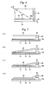
- Figs. 13(a) and (b) are cross-sectional views showing an example of the manufacturing steps of the base of the micro electromechanical relay.
- Figs. 14(a) and (b) are cross-sectional views showing an example of the manufacturing steps of the actuator of the micro electromechanical relay.
- Figs. 15(a)-(c) are cross-sectional views showing one example of the connecting steps of the base and the actuator.
- Figs. 16(a)-(c) are cross-sectional views showing an example of the manufacturing steps of the actuator.
- Figs. 17(a) and (c) are cross-sectional views showing an example of the connecting steps of the base and the actuator.
- Figs. 18(a)-(c) are cross-sectional views showing an example of the manufacturing steps of the actuator.
- Figs. 19(a) and (b) are cross-sectional views showing an example of the connecting steps of the base and the actuator.
- Fig. 20 shows a structure of a micro electromechanical relay according to an embodiment of the present invention. Fig. 20(a) is a top view. Fig. 20(b) of is a cross-sectional view of the D-D line shown in Fig. 20(a) viewed in the direction of the arrows.
- Fig. 21 is a top view schematically showing a micro electromechanical relay according to an embodiment of the present invention.
- Fig. 22 shows a state of the above-mentioned micro electromechanical relay when a voltage is not applied between the fixed electrode and the movable electrode. Fig. 22(a) is a cross-sectional view at the E-E line shown in Fig. 21 viewed in the direction of the arrows, and Fig. 22(b) is a cross-sectional view at the F-F line shown in Fig. 21 viewed in the direction of the arrows.
- Fig. 23 shows a state of the above-mentioned micro electromechanical relay when a voltage is applied between the fixed electrode and the movable electrode. Fig. 23(a) is a cross-sectional view at the E-E line shown in Fig. 21 viewed in the direction of the arrows, and FIG, 23(b) is a cross-sectional view at the F-F line shown in Fig. 21 viewed in the direction of the arrows.
- Fig. 24 is a top view of the relevant parts of the above-mentioned micro electromechanical relay.
- Figs. 25(a)-(d) show cross-sectional views of the G-G line shown in Fig. 24, viewed in the direction of the arrows, showing movement of the movable electrode due to electrostatic attraction.
- Fig. 26 is a top view of the relevant parts of a micro electromechanical relay according to an embodiment of the present invention.
- Fig. 27 is a cross-sectional view showing a structure of a micro electromechanical relay according to an embodiment of the present invention. Fig. 27(a) shows a state when a voltage is not applied between the fixed electrode and the movable electrode, and Fig. 27(b) shows a state when a voltage is applied.
- Figs. 28(a) and (b) are cross-sectional views showing an example of the manufacturing steps of the base of the above-mentioned micro electromechanical relay.
- Figs. 29(a)-(c) are cross-sectional views showing an example of the manufacturing steps of the actuator of the above-mentioned micro electromechanical relay.
- Figs. 30(a) and (b) are cross-sectional views showing an example of the connecting steps of the base and the actuator.
- Fig. 31(a) and (b) are cross-sectional views showing an example of the manufacturing steps of the actuator.
- Figs. 32(a) and (b) are cross-sectional views showing an example of the connecting steps of the base and the actuator.
- Figs. 33(a) and (b) are cross-sectional views showing an example of the manufacturing steps of the actuator.
- Fig. 34(a) and (b) are cross-sectional drawings showing an example of the connecting steps of the base and the actuator.
- Fig. 35 shows a structure of a micro electromechanical relay according to an embodiment of the present invention. Fig. 35(a) is a top view. Fig. 35(b) is a cross-sectional view of the H-H line shown in Fig. 35(a) viewed in the direction of the arrows.
- Fig. 36 is a block diagram schematically showing composition of a wireless radio according to an embodiment of the present invention.
- Fig. 37 is a block diagram schematically showing composition of a measurement instrument according to an embodiment of the present invention.
- Fig. 38 is a block diagram schematically showing composition of a temperature controller according to an embodiment of the present invention.
- Fig. 39 is a block diagram schematically showing the relevant composition of a portable data terminal according to an embodiment of the present invention.
- Fig. 40 is a top view showing schematically a conventional micro electromechanical relay.
- Fig. 41 shows a state of the conventional micro electromechanical relay when a voltage is not applied between the fixed electrode and the movable electrode. Fig. 41(a) is a cross-sectional view at the P-P line shown in Fig. 40 viewed in the direction of the arrows, and Fig. 41(b) is a cross-sectional view at the Q-Q line shown in Fig. 40 viewed in the direction of the arrows.
- Fig. 42 shows a state of the conventional micro electromechanical relay when a voltage is applied between the fixed electrode and the movable electrode. Fig. 42(a) is a cross-sectional view at the P-P line shown in Fig. 40 viewed in the direction of the arrows, and Fig. 42(b) is a cross-sectional view at the Q-Q line shown in Fig. 40 viewed in the direction of the arrows.
- Fig. 43 a top view of the relevant parts of the conventional micro electromechanical relay.
- Figs. 44(a)-(d) are cross-sectional views at the R-R line shown in Fig. 43, viewed in the direction of the arrows, showing movement of the movable electrode due to electrostatic attraction.
- Fig. 45 shows results of a simulation of the amount of displacement of the conventional movable electrode.
- An exemplary embodiment of the present invention will be explained with reference to Figs. 1-5. Fig. 1 shows schematically a micro electromechanical relay (micro electromechanical switch) according to the present embodiment. The micro
electromechanical relay 10 comprises abase 11 and anactuator 21 that is partially affixed to an upper face of the base at a portion and separated from the base 11 at the other portion. An element that is the same is designated by the same reference. These figures may emphasize specific parts for understanding of the invention. Thus, the various of dimensions of the microelectromechanical relay 10 shown in these figures are not restricted to reflecting the various of dimensions of an actual microelectromechanical relay 10. - The
base 11 is formed from a glass substrate such as Pyrex (Trademark). Upon the upper face of thebase 11, a pair ofsignal lines electrode 12 are formed from a conductor such as gold, copper, or aluminum. The pair ofsignal lines fixed contact 13a and afixed contact 14a are formed at the opposing parts of thesignal lines film 15 is formed on the fixedelectrode 12 for prevention of electrical short circuiting between the fixedelectrode 12 and themovable electrode 24. - The
actuator 21 is formed from a semiconductor substrate such as silicon. Theactuator 21 comprises a supportingportion 22, abeam portion 23, amovable electrode 24, and amovable contact portion 25. The supportingportion 22 is disposed on the face of thebase 11, extends upward therefrom, and supports thebeam portion 23, themovable electrode 24, and themovable contact portion 25. Thebeam portion 23 extends from the supportingportion 22 as a cantilever-like beam for elastically supporting themovable contact portion 25 as well as for elastically supporting themovable electrode 24 through a connectingpart 28. Themovable contact portion 25 is disposed at a distal tip of thebeam portion 23, and themovable electrodes 24 are disposed on both sides of thebeam portion 23 through the connectingpart 28. The connectingpart 28, thebeam portion 23, and themovable electrode 24 all have the same thickness. - The
movable electrode 24 is disposed at a position opposite to the fixedelectrode 12 of thebase 11. In the present embodiment, by cutting from an end of themovable electrode 24 that is located on a side where thebeam portion 23 extends from the supporting portion, aslit 27 is formed in the connectingpart 28 between themovable electrode 24 and thebeam portion 23. Thus, themovable electrode 24 and thebeam portion 23 are connected together at the side of themovable contact portion 25. - The
movable contact portion 25 is disposed at a position opposing a region extending from the fixedcontact 13a to the fixedcontact 14a. An insulating film (not illustrated) is formed at a lower face of themovable contact portion 25, and amovable contact 26, made from a conductor, is disposed on the insulating film. Themovable contact 26 opposes each of the fixedcontacts signal lines contacts - The micro
electromechanical relay 10 of the present embodiment has a duplex structure such that themovable contact 26 connects and separates the pair of fixedcontacts actuator 21 of the present embodiment supports themovable contact portion 25 from one side and thus is called a "cantilever-type actuator." - Figs. 2(a) and (b) show a state when a voltage is not applied between the fixed
electrode 12 and themovable electrode 24. In this case, as shown by the figure, themovable contact 26 is separated from the fixedcontact signal lines - Figs. 3(a) and (b) show a state when a voltage is applied between the fixed
electrode 12 and themovable electrode 24. In this case, as shown by the figure, themovable electrode 24 is driven by the fixedelectrode 12 due to electrostatic attraction caused by the applied voltage. Thus, themovable contact 26 comes into contact with the fixedcontact signal lines - According to the present embodiment, the
beam portion 23 and themovable electrode 24 are connected at the side of themovable contact portion 25, and theslit 27 opens from the side of the supportingportion 22. By way of this configuration, as shown in Figs. 3(a) and (b), most parts of themovable electrodes movable contact 25, come into contact with the fixedelectrode 12 through the insulatingfilm 15. The electrostatic attraction between themovable electrode 24 and the fixedelectrode 12 is inversely proportional to the square of the distance between themovable electrode 24 and the fixedelectrode 12, and therefore this electrostatic attraction becomes quite marked. Thus, even through the elastic constant of thebeam portion 23 increases, it is possible to raise the contact force imparted to themovable contact portion 25, and it is possible to stabilize the contact resistance between themovable contact 26 and the fixedcontacts - When the voltage between the fixed
electrode 12 and themovable electrode 24 disappears, the electrostatic attraction disappears. Thus, theactuator 21, due to restorative force of thebeam portion 23 and themovable electrode 24, returns to the original position as shown in Figs. 2(a) and (b). According to the present embodiment, as explained previously, it is possible to increase the elastic constant of thebeam portion 23. Thus, the restorative force imparted by thebeam portion 23 to themovable contact portion 25 can be increased, and it is possible to prevent undesirable contact between themovable contact 26 and the fixedcontacts - Various types of characteristics of the
movable electrode 24 of the present embodiment were investigated. The amount of displacement of themovable electrode 24 due to application of voltage depends on the elastic constant of the connectingpart 28 that interconnects thebeam portion 23 and themovable electrode 24. The elastic constant k of the connectingpart 28 is shown by the following equation.
portion 28a of the connectingpart 24 that connects themovable electrode 24 and thebeam portion 23. L is a gap length between themovable electrode 24 and thebeam portion 23 of the actual connectingportion 28a. H is the thickness of themovable electrode 24. The symbols W and L are shown in Fig. 1, and the symbol H is shown in Fig. 2(b). - Pull-in voltage is known as an indicator that shows the imparted voltage necessary to sufficiently attract the
movable electrode 24 to the fixedelectrode 12. The pull-in voltage is a voltage resulting in an inter-electrode distance of movable parallel electrodes plates that is 2/3rds of the initial distance. When the pull-in voltage is low, the applied voltage required for contacting most of themovable electrode 24 against the fixedelectrode 12 becomes low. - The pull-in voltage Vpi is expressed by the following equation.

- Further, the inter-electrode electrostatic attraction Fele is expressed by the following equation.

- Upon comparison of Figs. 1 and 2(b) with Figs. 40 and 41 (b), although thickness H and gap length L are equal for the micro
electromechanical relay 10 of the present embodiment in comparison to the conventional microelectromechanical relay 101, width W of the actual connectingportion 28a is understood to be shorter than the length of the conventional actual connecting portion (i.e., width W of the conventional contacting part 118). Thus, according to the above-mentioned Equation (1, the connectingpart 28 of the present embodiment can have a lower elastic constant than that of the conventional connectingpart 118. Further, according to the above-mentioned Equation (2), the pull-in voltage can be decreased without increasing the dimensions of themovable electrode 24. - Operation of the
movable electrode 24 due to application of voltage will be explained with reference to Figs. 4 and 5. Fig. 4 shows relevant parts of the microelectromechanical relay 10 of the present embodiment shown in Fig. 1. Further, Figs. 5(a)-(d) show cross-sectional views of the C-C line shown in Fig. 4 (i.e., from themovable electrode 24 to the movable contact portion 25) while themovable electrode 24 is moved by electrostatic attraction. - The
movable electrode 24 of the present embodiment is driven in the below described manner. Specifically, when a voltage is not applied, themovable electrode 24 is positioned as shown in Fig. 5 (a). Then, when a voltage is applied, firstly as shown in Fig. 5(b), a corner portion of themovable electrode 24 becomes displaced toward the fixedelectrode 12 by electrostatic attraction. At this time, as explained previously, the elastic constant of the connectingpart 28 is low, and the amount of deformation is high. Thus, the amount of displacement of themovable electrode 24 is large, and the corner portion comes into contact with the fixedelectrode 12 through the insulatingfilm 15. - Due to the large amount of displacement of the
movable electrode 24, the distance between themovable electrode 24 and the fixedelectrode 12 becomes small, and the electrostatic attraction increases further according to the above-mentioned Equation (3). Thus, as shown in Fig. 5(c), themovable electrode 24 and themovable contact portion 25 move toward thebase 11. At this time, since the amount of deformation of the connectingpart 28 is large, a decrease of the inter-electrode separation becomes greater, and also an increase of the amount of electrostatic attraction becomes greater. For this reason, the amount of displacement of themovable electrode 24 and themovable contact portion 25 is large, half of themovable electrode 24 comes into contact with the fixedelectrode 12 through the insulatingfilm 15, and therefore themovable contact 26 comes into contact with the fixedcontact 13a. - Due to the displacement of the
movable electrode 24 toward thebase 11, the distance between themovable electrode 24 and the fixedelectrode 12 becomes smaller, and electrostatic attraction increases further according to the above-mentioned Equation (3). Thus, as shown in Fig. 5(d), the most part of themovable electrode 24 comes into contact with the fixedelectrode 12 through the insulatingfilm 15. Since the most part of themovable electrode 24 contacts the fixedelectrode 12 through the insulatingfilm 15 in this manner, a sufficiently large electrostatic attraction acts upon themovable electrode 24, and the contact force between themovable contact 26 and the fixedcontact 13a becomes large, thereby resulting in stabilizing contact resistance. - Thus, it is possible to increase the electrostatic attraction by lowing the elastic constant of the connecting
part 28 while maintaining the restorative force unchanged. Accordingly, the contact force can be improved while maintaining a restorative force that is equivalent to the conventional micro electromechanical relay. Further, if the contact force may be equivalent to the conventional micro electromechanical relay, then it is possible to lower the electrostatic attraction, and thus it becomes possible to lower the applied voltage, decrease the dimensions of themovable electrode 24, or the like. - According to the present embodiment, the
movable electrodes 24 are disposed on both sides of themovable electrode 24. However, as shown in Fig. 4, it is also permissible to dispose a singlemovable electrode 24 on only one side of thebeam portion 23. However, since themovable contact portion 25 otherwise becomes displaced at a tilt relative to thebase 11, themovable electrodes beam portion 23. - A specific example of the micro
electromechanical relay 10 of the present embodiment will be explained while referring to Figs. 6-9. In this example, a longitudinal direction of thebeam portion 23 is referred to as the lengthwise direction, and a narrow direction perpendicular to the lengthwise direction is referred to as the width direction. In the microelectromechanical relay 10 according to the present working example, thebase 11 is formed from a glass substrate, and the fixedelectrode 12 and thesignal lines actuator 21 is formed from a silicon semiconductor substrate, and themovable contact 26 is formed from Au. - In addition, the various dimensions of the micro
electromechanical relay 10 are described below. Specifically, a length of thebeam portion 23 is 450 µm, and a width is 120 µm. Further, themovable electrode 24 is 410 µm long and 500 µm wide. Furthermore, thecontact part 28 has the same length (410 µm) as themovable electrode 24 and has a width of 40 µm With respect to the connectingpart 28, a length of theslit 27 is 310 µm, and a length W of the actual contactingportion 28a is 100 µm. Moreover, each thickness H of thebeam portion 23, themovable electrode 24, themovable contact portion 25, and thecontact part 28 is 21.15 µm Lastly, a distance between the fixedelectrode 12 and themovable electrode 24 when a voltage is not applied is 1.2 µm, and a distance between the fixedcontacts movable contact 26 is 1.0 µm. - Fig. 6 shows results of a simulation of the amount of displacement of the
actuator 21 when a voltage of 20V is applied to the microelectromechanical relay 10 of the present working example. When points of equal amount of displacement are interconnected by contour lines, the amount of displacement is indicated by densities of dots within regions bounded by the contour lines and the profile of themovable electrode 24. In other words, the region without dots indicates the region of near zero amount of displacement, and the region of highest density of dots indicates the region of contact between themovable electrode 24 and the fixedelectrode 12. - Referring still to Fig. 6, it may be understood that the amount of displacement is large for the
movable electrode 24 of the present working example, and themovable electrode 24 contacts nearly all of the fixedelectrode 12. Thus, due to the electrostatic attraction between the fixedelectrode 12 and themovable electrodes 24, the suppression force of themovable contact 26 against the fixedcontacts - Contact forces of the present working example and the comparative example will be examined in further detail with reference to Fig. 7-9. The comparative example is the conventional micro
electromechanical relay 100 shown in Fig. 40, and this microelectromechanical relay 100 has the same above-mentioned dimensions as those of the present working example except for theslit 27. In order to equate the restorative force of the present working example with that of the comparative example, each thickness H of thebeam portion 113, themovable electrode 114, and themovable contact 115 is taken to be 19.46 µm. Namely, in order to assure the same degree of restorative force as before for the microelectromechanical relay 10 of the present working example, the thicknesses H of thebeam portion 23, themovable electrode 24, themovable contact portion 25, and the connectingpart 28 are respectively increased. - Fig. 7 is a graph showing the relationship between contact force and applied voltage for the micro
electromechanical relay 10 of the present working example and the microelectromechanical relay 100 of the comparative example. It may be understood by referring to this figure that the microelectromechanical relay 10 of the present working example has markedly improved (9-fold) greater contact force than that of the conventional microelectromechanical relay 100, while restorative force is of the same degree as the conventional one. - The fact that the contact force becomes larger than zero means that the
movable contact 26 contacts the fixedcontacts electromechanical relay 10 of the present working example may be understood to enter the ON state at a lower applied voltage than that of the comparative example. - Referring still to Fig. 7, the contact force of the present working example at an applied voltage of 15V is understood to be higher than the contact force of the comparative example at an applied voltage of 20V. Thus, if it is permissible for the contact force to have the same magnitude as that used previously (0.21 mN), it is then possible to decrease the applied voltage by about 25% from about 20V to about 15V. This is equivalent to nearly halving the electrode surface area. As a result, it becomes possible to achieve a micro
electromechanical relay 10 that is smaller than the conventional one and / or that has a lower voltage. - Additionally, as shown in the above mentioned Equation (3), electrostatic attraction is proportional to the electrostatic capacitance. Electrostatic capacitance of the present working example is 29.31 pF, and electrostatic capacitance of the comparative example was 7.16 pF. Thus, the micro
electromechanical relay 10 of the present working example, in comparison to the conventional microelectromechanical relay 100, may be understood to have a markedly improved electrostatic attraction for the same applied voltage. - Figs. 8 and 9 show the relationship between the contact force and length of the
slit 27 for the microelectromechanical relay 10 of the present working example in tabular form and graphical form, respectively. Referring to the graph of Fig. 9, it may be understood that there is a dramatic improvement of contact force when the length of theslit 27 is greater than or equal to 150 µm. Thus, the length of theslit 27 is preferably greater than or equal to 150 µm (i.e., greater than or equal to about 37% of the length of the movable electrode 24). - Further, referring to the graph of Fig. 9, it may be understood that contact force becomes maximum when the length of the
slit 27 is 250 µm, and contact strength may be understood to be nearly the same for higher values of the length of theslit 27. Thus, the length greater than or equal to 250 µm (i.e., greater than or equal to about 60% of the length of the movable electrode 24) is further preferred for maintenance of stable contact force. Among lengths within this range, and in consideration of variance at the time of manufacture and strength of the actual contactingportion 28a, the length of theslit 27 is more preferably 280 - 370 µm or about 70% to about 90% of the length of themovable electrode 24. - Another embodiment of the present invention will be explained with reference to Fig. 10. The micro
electromechanical relay 10 according to the present embodiment differs from the microelectromechanical relay 10 shown in Fig. 1 in that a fixedelectrode 12 is disposed on either side of thesignal lines portion 22, thebeam portion 23, themovable electrode 24, and the connectingpart 28 are disposed on either side of themovable contact portion 28; while the composition is similar otherwise. Elements having the same function as those explained for the above-mentioned embodiment are designated by the same references, and further explanation of such elements will be omitted. - Fig. 10 shows schematically the micro
electromechanical relay 10 of the present embodiment. The illustratedactuator 21 supports themovable contact portion 25 from both sides and thus is called a "double-support type actuator." - The micro
electromechanical relay 10 of the present embodiment may have an effect similar to that of the microelectromechanical relay 10 shown in Fig. 1. Further, in comparison to the microelectromechanical relay 10 shown in Fig. 1, although the microelectromechanical relay 10 of the present embodiment requires space for placement of the fixedelectrodes 12, etc. at either side of thesignal lines movable contact portion 25 can be moved in the vertical direction while maintaining an approximately parallel attitude relative to thebase 11, it is possible to stabilize contact between themovable contact 26 and the fixedcontacts - An example of the micro
electromechanical relay 10 of the present embodiment will be explained with reference to Fig. 11. The microelectromechanical relay 10 of the present working example differs from the microelectromechanical relay 10 shown in Fig. 1 in that a fixedelectrode 12 is disposed on either side of thesignal lines portion 22, thebeam portion 23, themovable electrode 24, and the connectingpart 28 are disposed on either side of themovable contact portion 28; while the various dimensions and materials of the constituent elements are similar. - Fig. 11 shows the results of a simulation of the amount of displacement of the
movable electrode 24 when a voltage of 20V is applied to the microelectromechanical relay 10 of the present working example. The illustrated contour lines and dots have the same meanings as those of Fig. 6. - It may be understood by referring to Fig. 11 that the amount of displacement of the
movable electrode 24 of the present working example is large, and nearly the entire fixedelectrode 12 is contacted. It is thus understood, due to the electrostatic attraction between the fixedelectrode 12 and themovable electrode 24, that themovable contact 26 presses against the fixedcontacts - Yet another embodiment of the present invention will be explained while referring to Figs. 12-19. The micro
electromechanical relay 10 of the present embodiment differs from the microelectromechanical relay 10 shown in Fig. 1 only in that the actual connecting portion of the connectingpart 28 is different, while the composition is otherwise similar. Elements having the same function as those explained for the above mentioned embodiments are designated by the same references, and further explanation of such elements will be omitted. - Fig. 12 shows schematically the micro
electromechanical relay 10 of the present embodiment. As shown in this figure, the microelectromechanical relay 10 of the present embodiment differs from the microelectromechanical relay 10 shown in Fig. 1 in that the material and / or structure of the actual connectingportion 28a of the connectingpart 28 are different; and also the material and / or structure of thebeam portion 23 and themovable electrode 24 are different. By way of this it is readily possible to change the width and / or thickness of the actual connectingportion 28b according to the material and / or structure of the actual connectingportion 28b, and thus this may expand the possibility of design of the actual connectingportion 28b. - Example configurations of the actual connecting
portion 28b that can be cited are: the actual connectingportion 28b formed from stacked films, the actual connectingportion 28b formed by applying a conductive material and then removing the material down to a single layer, or the like. - A method of manufacture of the micro
electromechanical relay 10 of the above-mentioned structure will be explained with reference to Fig. 13 - Fig. 15. - Figs. 13(a) and (b) show an example of the manufacturing steps of the
base 11. Firstly, as shown in 13(a), aglass substrate 11a of Pyrex (Trademark) or the like is prepared. Thereafter, as shown in 13(b), a metal film is formed on theglass substrate 11 a, and the fixedelectrode 12 and thesignal lines base 11 is completed by formation of the insulatingfilm 15 on the fixedelectrode 12. If a silicon oxide film of a specific dielectric constant of 3-4 or a silicon nitride film of a specific dielectric constant of 7-8 is used as theinsulation film 15, the obtained electrostatic attraction is high, and it is possible to increase contact force. - Figs. 14(a) and (b) show one example of the manufacturing steps of the
actuator 21. Firstly, as shown in Fig. 14 (a), a SOI (Silicon On Insulator)wafer 30 is prepared. Thereafter, as shown in Fig. 14(b), the silicon oxide film, for example, is etched using TMAH (tetramethyl ammonium hydroxide), while using the silicon oxide film as a mask, to form the supportingportion 22. Thereafter, an insulation film and a metal film are formed, and the pattern of themovable contact 26 is formed. - Figs. 15(a)-(c) show an example of the steps of bonding the
base 11 and theactuator 21. Firstly, as shown in Fig. 15(a), theSOI wafer 30 is bonded to thebase 11 by the anodic bonding method to form a single unit. Thereafter, as shown in 15(b), the upper face of theSOI wafer 30 is etched by an alkali etching solution (e.g., TMAH, KOH, or the like) such that etching occurs down to the silicon oxide (SiO2)film 31. Then, as shown in Fig. 15(c), thesilicon oxide film 31 in a region other than that corresponding to the actual connectingportion 28a of the connectingpart 28 is removed by a fluorine type etching solution to expose thebeam portion 23, themovable electrode 24, and themovable contact portion 25. Thereafter, dry etching using RIE (Reactive Ion Etching) or the like is carried out to form theslit 27 and the required etched-away parts (not illustrated) to complete the microelectromechanical relay 10. - Thus, the actual connecting
portion 28b of the connectingpart 28 manufactured by the manufacturing method shown in Figs. 13-15, as shown in Fig. 15 (c), has a layered structure comprising a compression-stressed film ofsilicon oxide film 31 formed on the same silicon layer as that of thebeam portion 23 and themovable electrode 24. - Another manufacturing method of the micro
electromechanical relay 10 of the above mentioned composition will be explained while referring to Fig. 16 and 17. The manufacturing steps of the base 11 are the same as those shown in Fig. 13, and thus explanation of these steps will be omitted. - Figs. 16(a)-(c) show one example of the manufacturing steps of the
actuator 21. Firstly, as shown in Fig. 16(a), theSOI wafer 30 is prepared. Thereafter, as shown in Fig. 16(b), the silicon oxide film, for example, is etched using TMAH, while using the silicon oxide film as a mask of the upper face of theSOI wafer 30, to form the supportingportion 22. Thereafter, as shown in Fig. 16(c), an insulation film and a metal film are formed, and the pattern of themovable contact 26 is formed. Simultaneous with this step, a metal film pattern is formed also in the region corresponding to the actual connectingportion 28b of the connectingpart 28. - Figs. 17(a) and (b) show an example of the steps of bonding the
base 11 and theactuator 21. Firstly, as shown in drawing (a) of the same figure, theSOI wafer 30 is bonded to thebase 11 by the anodic bonding method to form a single unit. Thereafter, as shown in Fig. 17(b), the upper face of theSOI wafer 30 is etched by an alkali etching solution (e.g., TMAH, KOH, or the like) to etch down to thesilicon oxide film 31. Also, thesilicon oxide film 31 is removed by a fluorine type etching solution to expose thebeam portion 23, themovable electrode 24, and themovable contact portion 25. Thereafter, dry etching using RIE or the like is carried out to form theslit 27 and the required etched-away parts (not illustrated) to complete the microelectromechanical relay 10. - Thus, the actual connecting
portion 28b of the connectingpart 28 manufactured by the manufacturing method shown in Figs. 16 and 17, as shown in Fig. 17(b), has a layered structure comprising the silicon layer of both thebeam portion 23 and themovable electrode 24 and themetal film 32 formed on the base 11 side. - Another manufacturing method of the micro
electromechanical relay 10 of the above mentioned composition will be explained with reference to Figs. 18 and. 19. The manufacturing steps of the base 11 are the same as those shown in Fig. 13, and thus explanation of these steps will be omitted. - Figs. 18(a)-(c) show one example of the manufacturing steps of the
actuator 21. Firstly, as shown in Fig. 18(a), theSOI wafer 30 is prepared. Thereafter, as shown in Fig. 18(b), the silicon oxide film, for example, is etched using TMAH, while using the silicon oxide film as a mask of the upper face of theSOI wafer 30, to form the supportingportion 22. Also, a region corresponding to the actual connectingportion 28b of the connectingpart 28 is etched to expose thesilicon oxide film 31. Thereafter, as shown in Fig. 18(c), an insulation film and a metal film are formed, and the pattern of themovable contact 26 is formed. Simultaneous with this step, ametal film 33 pattern is formed also in a recess corresponding to the actual connectingportion 28b of the connectingpart 28. - Figs. 19(a) and (b) show one example of the steps of bonding the
base 11 and theactuator 21. Firstly, as shown in Fig. 19(a), theSOI wafer 30 is bonded to thebase 11 by the anodic bonding method to form a single unit. Thereafter, as shown in Fig. 19(b), the upper face of theSOI wafer 30 is etched by an alkali etching solution (e.g. TMAH, KOH, or the like) to etch down to thesilicon oxide film 31. Also, thesilicon oxide film 31 is removed by a fluorine type etching solution to expose thebeam portion 23, themovable electrode 24, and themovable contact portion 25. Thereafter, dry etching using RIE or the like is carried out to form theslit 27 and the required etched-away parts (not illustrated) to complete the microelectromechanical relay 10. - Thus, the actual connecting
portion 28b of the connectingpart 28 manufactured by the manufacturing method shown in Figs. 18 and 19, as shown in Fig. 19(b), has a single-layer structure formed by themetal film 33 from a different material than that of thebeam portion 23 and themovable electrode 24. - Another embodiment of the present invention will be explained with reference to Fig. 20. The micro
electromechanical relay 10 of the present embodiment differs from the microelectromechanical relay 10 shown in Fig. 1 in that the contact structure is a singleplex structure, while the composition is otherwise similar. Elements having the same function as those explained for the above mentioned embodiments are designated by the same references, and further explanation of such parts will be omitted. - Fig. 20 shows schematically the micro
electromechanical relay 10 of the present embodiment. As per this figure, the microelectromechanical relay 10 of the present embodiment differs from the microelectromechanical relay 10 shown in Fig. 1 in that the signals lines 13 and 14 are disposed on the base 11 co-linearly with thebeam portion 23 so that the signals lines 13 and 14 are sandwiched between the fixedelectrodes 12. The part of thesignal line 13 opposite to thesignal line 14 serves as thefixed contact 13a. - A
signal line 35, formed from an electrical conductor through an intermediary insulating film (not illustrated), is formed at a bottom surface of the actuator 21 from the center of the supportingportion 22 along thebeam portion 23 to themovable contact portion 25. Thesignal line 35 is connected electrically to thesignal line 14 of thebase 11, and the bottom surface part of the movable contact portion 25 (i.e., the part opposite to the fixedcontact 13a of the signal line 13) serves as amovable contact 35a. - When a voltage is applied between the
movable electrode 24 and the fixedelectrode 12 of the microelectromechanical relay 10 of the above mentioned composition, themovable contact portion 25 moves, and themovable contact 35a and the fixedcontact 13a come into mutual contact. By way of this, thesignal lines signal line 35. The present embodiment has the singleplex structure, wherein themovable contact 35a contacts and separates from a single fixedcontact 13a. The microelectromechanical relay 10 of the present embodiment has improved contact reliability due to a low number of contacts in comparison to the microelectromechanical relay 10 shown in Fig. 1. - Another embodiment of the present invention will be explained while referring to Figs. 21-25. The micro
electromechanical relay 10 of the present embodiment differs from the microelectromechanical relay 10 shown in Fig. 1 in that composition of the connectingpart 28 is different, while the structure is otherwise similar. Elements having the same function as those explained for the above mentioned embodiments are designated by the same references, and further explanation of such elements will be omitted. - Fig. 21 shows schematically the micro
electromechanical relay 10 of the present embodiment. Referring to Fig. 21, the microelectromechanical relay 10 of the present embodiment differs from the microelectromechanical relay 10 shown in Fig. 1 in thatgrooves 50 are formed in the connectingpart 28 in the interval between themovable electrode 24 and thebeam portion 23. - Figs. 22(a) and (b) show a state when a voltage is not applied between the fixed
electrode 12 and themovable electrode 24. In this case, as shown in these figures, themovable contact 26 is separated from the fixedcontacts signal line 13 and thesignal line 14 are mutually separated electrically. - Figs. 23(a) and (b) show a state when voltage is applied between the fixed
electrode 12 and themovable electrode 24. As shown in these figures, themovable electrode 24 is driven toward the fixedelectrode 12 due to electrostatic attraction generated by the above mentioned application of voltage. Thus, themovable contact 26 contacts the fixedcontacts signal line 13 and thesignal line 14 are mutually connected electrically. - According to the present embodiment,
grooves 50 are formed in the connectingpart 28. Since thegroves 50 are thin in comparison to thebeam portion 23 and themovable electrode 24, the elastic constant is lower than that of the conventional configuration, and deformation occurs more readily. Thus, as shown in Figs. 23(a) and (b), with the exception of the region near thebeam portion 23, most parts of themovable electrode 24 contact the fixedelectrode 12 through the insulatingfilm 15 due to the increased bending according to thegrooves 50. In this case, the electrostatic attraction between themovable electrode 24 and the fixedelectrode 12 is inversely proportional to the square of the distance between themovable electrode 24 and the fixedelectrode 12. Thus, the electrostatic attraction becomes markedly increased. Accordingly, even though the elastic constant of thebeam portion 23 becomes large, it is possible to increase the contact force imparted to themovable contact portion 25, and it is possible to stabilize resistance between themovable contact 26 and the fixedcontacts - When the voltage between the fixed
electrode 12 and themovable electrode 24 disappears, the electrostatic attraction disappears, and theactuator 21 returns to the original position shown in Figs. 22(a) and (b) due to the restorative force of thebeam portion 23, themovable electrode 24, and thegrooves 50. - Driving of the
movable electrode 24 due to application of voltage will be explained with reference to Figs. 24 and 25. Fig. 24 shows relevant parts of the microelectromechanical relay 10 of the present embodiment shown in Fig. 21. Further, Figs. 25(a)-(d) are cross-sectional drawings of the C-C line shown in Fig. 24 (i.e., from themovable electrode 24 to the movable contact portion 25) showing movement of themovable electrode 24 due to electrostatic attraction. - The
movable electrode 24 of the present embodiment operates in the below described manner. Specifically, when a voltage is not applied, themovable electrode 24 is positioned as shown in Fig. 25(a). Thereafter, when a voltage is applied, firstly as shown in Fig. 25(b), themovable electrode 24 becomes displaced toward the fixedelectrode 12 due to electrostatic attraction. At this time, as explained previously, the amount of deformation of thegrooves 50 of the present embodiment is high due to the small elastic constant. Thus, the amount of displacement of themovable electrode 24 increases, and the corner portion of themovable electrode 24 contacts the fixedelectrode 12 through the insulatingfilm 15. - Since the amount of displacement of the
movable electrode 24 is high, the distance between themovable electrode 24 and the fixedelectrode 12 becomes small, and the electrostatic attraction increases according to the above-mentioned Equation (3). Thus, as shown in Fig. 25(c), themovable electrode 24 and themovable contact portion 25 move toward thebase 11. At this time, since the amount of deformation of thegrooves 50 of the present embodiment is large, the above-mentioned inter-electrode distance decreases greatly, and increase of electrostatic attraction is greater. Thus, the amount of displacement of themovable electrode 24 and themovable contact portion 25 is large. Also, half of themovable electrode 24 comes into contact with the fixed electrode through the insulatingfilm 15, and therefore themovable contact 26 comes into contact with the fixedcontact 13a. - Due to movement of the
movable electrode 24 toward thebase 11, the distance between themovable electrode 24 and the fixedelectrode 12 becomes small, and the electrostatic attraction increases further according to the above-mentioned Equation (3). Thus, as shown in Fig. 25(d), themovable electrode 24 and themovable contact portion 25 move further toward thebase 11. Due to this movement, since the major part of themovable electrode 24 contacts the fixedelectrode 12 through the insulatingfilm 15, resulting in a marked increase of the electrostatic attraction acting on themovable electrode 24. Accordingly, the contact force between themovable contact 26 and the fixedcontact 13a becomes large, and thereby contact resistance is stabilized. - Thus, it is possible to increase the electrostatic attraction by decreasing the elastic constant of the connecting
part 28 while maintaining the restorative force unchanged. Further, it is possible to improve the contact force while maintaining restorative force equivalent to that used previously. If the contact force may be equivalent to that used previously, then it is possible to lower the electrostatic attraction, and thus it becomes possible to lower the applied voltage, decrease the dimensions of themovable electrode 24, or the like. - According to the present embodiment, the
movable electrodes 24 are disposed of either side of thebeam portion 23. However, as shown in Fig. 24, it is also possible to dispose themovable electrode 24 only at one side of thebeam portion 23. However, themovable electrodes beam portion 23 in order to move themovable contact portion 25 without tilt with respect to thebase 11. - Another embodiment of the present invention will be explained with reference to Fig. 26. The micro
electromechanical relay 10 of the present embodiment differs from the microelectromechanical relay 10 shown in Fig. 21 in that the fixedelectrodes 12 are disposed on either side of thesignal lines portion 22, thebeam portion 23, themovable electrode 24, and the connectingpart 28 are disposed on either side of themovable contact 25; whereas the composition is otherwise similar. Elements having the same function as those explained for the above mentioned embodiments are designated by the same references, and further explanation of such elements will be omitted. - Fig. 26 shows schematically the micro
electromechanical relay 10 of the present embodiment. The illustratedactuator 21 is a double-support type actuator that supports themovable contact portion 25 from both sides. - The micro
electromechanical relay 10 of the present embodiment may have a similar useful effect as that of the microelectromechanical relay 10 shown in Fig. 21. Furthe, the microelectromechanical relay 10 of the present embodiment differs from the microelectromechanical relay 10 shown in Fig. 21 in that although space is required for placement of the fixedelectrode 12, etc. on either side of thesignal lines movable contact portion 25 can be moved vertically while maintaining a roughly parallel attitude relative to thebase 11. It is thus possible to stabilize contact between themovable contact 26 and the fixedcontacts 13a and 14b. Moreover, it is possible to suppress unevenly distributed abrasion of the contact parts. - Another embodiment of the present invention will be explained with reference to Figs. 27-34. The micro
electromechanical relay 10 of the present embodiment differs from the microelectromechanical relay 10 shown in Fig. 21 in that a structure of the connecting parts is different, whereas the remaining structure is otherwise similar. Elements having the same function as those explained for the above mentioned embodiments are designated by the same references, and further explanation of such elements will be omitted. - Figs. 27(a) and (b) show a structure of the micro
electromechanical relay 10 of the present working embodiment. As shown in these figure, the microelectromechanical relay 10 of the present embodiment differs from the microelectromechanical relay 10 shown in Fig. 21 in that the connectingpart 51 connecting thebeam portion 23 and themovable electrode 24 comprises a conductor or semiconductor that has a smaller elastic constant than the conventional connecting part that thebeam portion 23 or themovable electrode 24 would extend. By way of this, the width or thickness of the connectingpart 51 can be readily changed according to the material and / or structure of the connectingpart 51. This may expand the possibility of design of the connectingpart 51. As an example of structure of the connecting part, the connectingpart 51 may be formed from stacked films. Alternatively, the connectingpart 51 may be formed by applying a conductive material and then removing the material down to a single layer. - A method for manufacture of the micro
electromechanical relay 10 of the above mentioned composition will be explained while referring to Figs. 28-30. - Figs. 28(a) and (b) show one example of the manufacturing steps of the
base 11. Firstly, as shown in Fig. 28(a), aglass substrate 11a of Pyrex (Trademark) or the like is prepared. Thereafter, as shown in Fig. 28(b), a metal film is formed on theglass substrate 11a, and the fixedelectrode 12 and thesignal lines base 11 is completed by formation of the insulatingfilm 15 on the fixedelectrode 12. If a silicon oxide film of a specific dielectric constant of 3-4 or a silicon nitride film of a specific dielectric constant of 7-8 is used as theinsulation film 15, the obtained electrostatic attraction is high, and it is possible to increase contact force. - Figs. 29(a)-(c) show one example of the manufacturing steps of the
actuator 21. Firstly, as shown in Fig. 29(a), theSOI wafer 30 is prepared. Thereafter as shown in Fig. 29(b), the silicon oxide film, for example, is etched using TMAH, while using the silicon oxide film as a mask, to form the supportingportion 22. Further, etching is carried out in the region corresponding to the connectingpart 51, and thesilicon oxide film 31 is exposed. Thereafter, as shown in Fig. 29(c), an insulation film and a metal film are formed, and the pattern of themovable contact 26 is formed. Simultaneous with this patterning step, the pattern of ametal film 60 is also formed in a region corresponding to the connectingpart 51. - Figs. 30(a) and (b) show one example of manufacturing steps of the
base 11 and theactuator 21. Firstly, as shown in Fig. 30(a), theSOI wafer 30 is bonded to thebase 11 by the anodic bonding method to form a single unit. Thereafter, as shown in Fig. 30(b), the upper face of theSOI wafer 30 is etched by an alkali etching solution (e.g., TMAH, KOH, or the like) such that etching occurs down to the silicon oxide (SiO2)film 31, and further etching using a fluoride type etching solution removes thesilicon oxide film 31 to expose thebeam portion 23, themovable electrode 24, themovable contact portion 25, and the connectingpart 51. Thereafter, dry etching using RIE or the like is carried out to form the required etched-away parts (not illustrated) to complete the microelectromechanical relay 10. - Thus, the connecting
part 51 manufactured by the manufacturing method shown in Figs. 28-30, as shown in Fig. 30(b), produces a single-layer structure from ametal film 33 that is a different material from that of thebeam portion 23 and themovable electrode 24. - Another method for the manufacture of the micro
electromechanical relay 10 will be described while referring to Figs. 31 and 32. The manufacturing steps of the base 11 are the same as the manufacturing steps shown in Fig. 28, and thus explanation of these manufacturing steps will be omitted. - Figs. 31 (a) and (b) show one example of the manufacturing steps of the
actuator 21. Firstly, as shown in Fig. 31(a), theSOI wafer 30 is prepared. Thereafter, as shown in Fig. 31 (b), the silicon oxide film, for example, is etched using TMAH, while using the silicon oxide film as a mask, to form the supportingportion 22. Thereafter, an insulation film and a metal film are formed, and the pattern of themovable contact 26 is formed. - Figs. 32(a) and (b) show one example of manufacturing steps of the
base 11 and theactuator 21. Firstly, as shown in Fig. 32(a), theSOI wafer 30 is bonded to thebase 11 by the anodic bonding method to form a single unit. Thereafter, as shown in Fig. 32(b), the upper face of theSOI wafer 30 is etched by an alkali etching solution (e.g., TMAH, KOH, or the like) such that etching occurs down to the silicon oxide (SiO2)film 31, and further etching using a fluoride type etching solution removes thesilicon oxide film 31 outside of the region corresponding to the connectingpart 51 to expose thebeam portion 23, themovable electrode 24, and themovable contact portion 25. Thereafter, dry etching using RIE or the like is carried out to form the required etched-away parts (not illustrated) to complete the microelectromechanical relay 10. - Thus, the connecting
part 51 manufactured by the manufacturing method shown in Figs. 31-32, as shown in Fig. 32 (b), has a layered structure comprising a compression-stressed film ofsilicon oxide film 31 formed on the same silicon layer as that of thebeam portion 23 and themovable electrode 24. - Another method for the manufacture of the micro
electromechanical relay 10 will be described while referring to Figs. 33 and 34. The manufacturing steps of the base 11 are the same as the manufacturing steps shown in Fig. 28, and thus explanation of these manufacturing steps will be omitted. - Figs. 33(a) and (b) show one example of manufacturing steps of the
actuator 21. Firstly, as shown in Fig. 33(a), theSOI wafer 30 is prepared. Thereafter, as shown in Fig. 33(b), the upper face of theSOI wafer 30 is etched, for example, is etched using TMAH, while using the silicon oxide film as a mask, to form the supportingportion 22. Thereafter, an insulation film and a metal film are formed, and the pattern of themovable contact 26 is formed. Simultaneous with this patterning step, the pattern of ametal film 62 is also formed in a region corresponding to the connectingpart 51. - Figs. 34(a) and (b) show one example of manufacturing steps of the
base 11 and theactuator 21. Firstly, as shown in Fig. 34(a), theSOI wafer 30 is bonded to thebase 11 by the anodic bonding method to form a single unit. Thereafter, as shown in Fig. 34(b), the upper face of theSOI wafer 30 is etched by an alkali etching solution (e.g., TMAH, KOH, or the like) such that etching occurs down to the silicon oxide (SiO2)film 31, and further etching using a fluoride type etching solution removes thesilicon oxide film 31 to expose thebeam portion 23, themovable electrode 24, and themovable contact portion 25. Thereafter, dry etching using RIE or the like is carried out to form the required etched-away parts (not illustrated) to complete the microelectromechanical relay 10. - Thus, the connecting
part 51 manufactured by the manufacturing method shown in Figs. 33 and 34, as shown in Fig. 34(b), has a layered structure comprising the same silicon layer that forms thebeam portion 23 and themovable electrode 24 and themetal film 62 that is formed on the surface of the silicon layer that faces thebase 11. It is also permissible to use another tensile-stress film (e.g., SiN, etc.) in place of themetal film 62. - Another embodiment of the present invention will be explained with reference to Fig. 35. The micro
electromechanical relay 10 of the present embodiment differs from the microelectromechanical relay 10 shown in Fig. 21 in that the contact structure is a singleplex structure. Elements having the same function as those explained for the above-mentioned embodiments are designated by the same references, and further explanation of such elements will be omitted. - Fig. 35 shows schematically the micro
electromechanical relay 10 of the present embodiment. As shown in this figure, thesignal lines base 11 of the microelectromechanical relay 10 co-linearly with thebeam portion 23 so that the signals lines 13 and 14 sandwich the fixedelectrodes 12. The part of thesignal line 13 opposite to thesignal line 14 serves as thefixed contact 13a. - A
signal line 35, formed from an electrical conductor through an intermediary insulating film (not illustrated), is formed at the bottom face of the actuator 21 from the center of the supportingportion 22 along thebeam portion 23 to themovable contact portion 25. Thesignal line 35 is connected electrically to thesignal line 14 of thebase 11, and the bottom face part of the movable contact portion 25 (i.e., the part opposite to the fixedcontact 13a of the signal line 13) serves as amovable contact 35a. - When a voltage is applied between the
movable electrode 24 and the fixedelectrode 12 of the microelectromechanical relay 10, themovable contact portion 25 moves, and themovable contact 35a and the fixedcontact 13a contact one another. Thus, thesignal lines signal line 35. The microelectromechanical relay 10 of the present embodiment has a singleplex structure, wherein themovable contact 35a contacts and separates from a single fixedcontact 13a. The microelectromechanical relay 10 of the present embodiment has improved contact reliability due to a low number of contacts in comparison to the microelectromechanical relay 10 shown in Fig. 21. - Another embodiment of the present invention will be explained next with reference to Fig. 36. Fig. 36 schematically shows a configuration of a
wireless radio 71 of the present embodiment. A microelectromechanical relay 72 of thewireless radio 71 connects together aninternal processing circuit 73 and anantenna 74. By way of ON/OFF switching of the microelectromechanical relay 72, there is switching of theinternal processing circuit 73 between a state capable of signal transmission or reception through theantenna 74 and a state incapable of signal transmission or reception. - According to the present embodiment, any of the micro
electromechanical relays 10 shown in Fig. 1 - Fig. 35 can be used as the microelectromechanical relay 72. Thus, the operational voltage of the microelectromechanical relay 72 can be lowered and also the shape and size of the microelectromechanical relay 72 can be downsized. Accordingly, it becomes possible to lower power consumption and reduce the size of thewireless radio 71. - Another embodiment of the present invention will be explained with reference to Fig. 37. Fig. 37 schematically shows a configuration of a
measurement instrument 75 of the present embodiment. A multiplicity of microelectromechanical relays 72 are interposed within a multiplicity ofsignal lines 77, respectively, between a singleinternal processing circuit 76 and a multiplicity of to-be-measured objects 78. By way of ON/OFF switching of each of the microelectromechanical relays 72, there is switching of theinternal processing circuit 76 between the to-be-measured objects 78 for signal transmission or reception. - According to the present embodiment, any of the micro
electromechanical relays 10 shown in Figs. 1-35 can be used as the microelectromechanical relay 72. Thus, the operational voltage of the microelectromechanical relay 72 can be lowered, and also the shape and size of the micro electromechanical relay can be downsized. Accordingly, it becomes possible to lower power consumption and reduce the size of themeasurement instrument 75. - Another embodiment of the present invention will be explained next while referring to Fig. 38. Fig. 38 schematically shows a configuration of a temperature controller (temperature sensor) 81 of the present embodiment. The
temperature controller 81 is installed in a device (referred to hereinafter simply as a "subject device") 82 that requires a safety function with respect to temperature (e.g., electrical power supply device, controller, or the like) for control of temperature of thesubject device 82. As shown in the figure, based on temperature of thesubject device 82, thetemperature controller 81 is equipped with the microelectromechanical relay 72 for ON/OFF switching of electrical power supply to aninternal circuit 83 of thesubject device 82. - For example, one case that may be considered of an operating condition of the
subject device 82 is the provision that operation should be within a time interval of 1 hour when temperature is greater than or equal to 100°C. When thetemperature controller 81 measures the temperature of thesubject device 82 and senses that thesubject device 82 has run for 1 hour at a temperature greater than or equal to 100°C, the microelectromechanical relay 72 within thetemperature controller 82 interrupts the supply of electricity to theinternal circuit 83 of thesubject device 82. - According to the present embodiment, any of the micro
electromechanical relays 10 shown in Fig. 1 - Fig. 35 can be used as the microelectromechanical relay 72. Thus, the operational voltage of the microelectromechanical relay 72 can be lowered, and also the shape and size of the microelectromechanical relay 72 can be downsized. Accordingly, it becomes possible to lower power consumption and reduce the size of thetemperature controller 81. - Another embodiment of the present invention will be explained with reference to Fig. 39. Fig. 39 schematically shows a relevant configuration of a
portable data terminal 85 of the present embodiment. The portable data terminal utilizes a pair of microelectromechanical relays electromechanical relay 72a switches between aninternal antenna 86 and anexternal antenna 87, and the (other) microelectromechanical relay 72b switches between a signal transmission circuit-sideelectrical power amplifier 88 and a signal reception circuit-side low noise amplifier 89. - According to the present embodiment, any of the micro
electromechanical relays 10 shown in Figs. 1-35 can be used as the microelectromechanical relays electromechanical relays electromechanical relays portable data terminal 85. - As explained above, the micro
electromechanical relay 10 according to the present invention, while maintaining restorative force equivalent to that used previously, is capable of improving contact force, lowering applied voltage, and / or reducing dimensions of the electrodes. Thus, by use of the microelectromechanical relay 10 of the present embodiment for various types of devices (e.g., wireless radio, measurement instrument, temperature controller, portable data terminal, or the like), power consumption and size of the device can be reduced. - The present invention is not limited to the above-mentioned embodiments, and various types of modifications are possible within the scope of the claims. Embodiments obtained by suitable combination of the technical means disclosed in different respective embodiments are also covered by the scope of the present invention.
- For example, although the above-mentioned embodiments explained the micro electromechanical relay, the present invention can be used appropriately for any type of micro electromechanical switch that opens and closes an electrical circuit by causing contact and separation between contacts by the use of electrostatic attraction.
- Further, according to the above mentioned embodiments, width of the
movable contact portion 25 was greater than width of thebeam portion 23. This may allow easy distinction between themovable contact portion 25 and thebeam portion 23. It is also permissible for the width of themovable contact portion 25 to be the same or smaller than the width of thebeam portion 23. - Furthermore, according to the above mentioned embodiments, most parts of the
beam portion 23 oppose the fixedelectrode 12, and when a voltage is applied between thebeam portion 23 and the fixedelectrode 12, thebeam portion 23 is driven toward the fixedelectrode 12 by electrostatic attraction. Thus, the portion of thebeam 23 opposite to the fixedelectrode 12 has a function as themovable electrode 24. - As explained above, the micro electromechanical switch according to the present invention, while maintaining restorative force equivalent to that used previously, is capable of improving contact force, lowering applied voltage, and / or reducing dimensions of the electrodes. Thus, the micro electromechanical switch according the present invention is suitable for use as a MEMS element requiring low electrical power consumption, size reduction, or the like.
Claims (23)
- An electromechanical switch comprising:a base;a fixed contact disposed on the base;a fixed electrode disposed on the base;an actuator comprising a supporting portion disposed on the base, a beam portion extending from the supporting portion, and a movable electrode connected to the beam portion and facing the fixed electrode, wherein the beam portion is displaced in accordance with a displacement of the movable electrode by electrostatic attraction caused between the fixed electrode and the movable electrode; anda movable contact disposed on an end portion of the beam portion and facing the fixed contact so as to come into contact with the fixed contact based on the displacement of the beam portion,wherein a slit is configured between the beam portion and the movable electrode.
- The electromechanical switch according to claim 1, wherein the slit is elongated between the beam portion and the movable electrode to an end portion of the movable electrode that is located on a side where the beam portion extends from supporting portion.
- The electromechanical switch according to claim 2, wherein the slit is configured such that the movable electrode is disconnected from the beam portion on the side where the beam portion extends from supporting portion.
- The electromechanical switch according to claim 2, wherein the end portion of the movable electrode that is located on the side is configured to be freely movable with respect to the beam portion.
- The electromechanical switch according to claim 1, wherein the movable electrode is configured such that an outer portion of the movable electrode is displaced toward the fixed electrode initially by the electrostatic attraction.
- The electromechanical switch according to claim 1, wherein a length of the slit is approximately 37 % or more of a length of the movable electrode in a direction extending along the beam portion.
- The electromechanical switch according to claim 6, wherein a length of the slit is approximately 60 % or more of a length of the movable electrode in a direction extending along the beam portion.
- The electromechanical switch according to claim 7, wherein a length of the slit is approximately 70 % or more of a length of the movable electrode in a direction extending along the beam portion.
- The electromechanical switch according to claim 6, wherein a length of the slit is approximately between 70 % and 90 % of a length of the movable electrode in a direction extending along the beam portion.
- The electromechanical switch according to claim 1, wherein the slit does not fully penetrated a thickness of the beam portion and the movable electrode.
- The electromechanical switch according to claim 1, wherein a portion at which the beam portion and the movable electrode are connected is different in at least one of material and structure from other portions of at least one of the beam portion and the movable electrode.
- The electromechanical switch according to claim 11, wherein the portion at which the beam portion and the movable electrode are connected is different in at least one of material and structure from all other portions of at least one of the beam portion and the movable electrode.
- A device used for switching on and off an electrical circuit, the device comprising the electromechanical switch according to claim 1.
- An electromechanical switch comprising:a base;a fixed contact disposed on the base;a fixed electrode disposed on the base;an actuator comprising a supporting portion disposed on the base, a beam portion extending from the supporting portion, a movable electrode facing the fixed electrode, and a connecting portion connecting the beam portion and the movable electrode, wherein the beam portion is displaced in accordance with a displacement of the movable electrode by electrostatic attraction caused between the fixed electrode and the movable electrode; anda movable contact disposed on an end portion of the beam portion and facing the fixed contact so as to come into contact with the fixed contact based on the displacement of the beam portion,wherein an elastic constant of the connecting portion is smaller than an elastic constant of at least one of the beam portion and the movable electrode.
- The electromechanical switch according to claim 14, wherein the connecting portion is different in at least one of material and structure from other portions of at least one of the beam portion and the movable electrode.
- The electromechanical switch according to claim 15, wherein the connecting portion is different in at least one of material and structure from all other portions at least one of the beam portion and the movable electrode.
- The electromechanical switch according to claim 15, wherein the connecting portion is configured to be thinner than at least one of the beam portion and the movable electrode.
- The electromechanical switch according to claim 15, wherein the connecting portion is configured to be layered.
- A method of manufacturing an electromechanical switch comprising:forming a base;bonding onto the base an SOI wafer so as to form an actuator, wherein the SOI wafer includes an oxide silicon layer disposed between an upper layer and a lower layer;removing the upper layer by etching to expose the oxide silicon layer;removing a portion by etching to leave a predetermined portion of the exposed oxide silicon layer;forming a beam portion and a movable electrode of the actuator by etching the lower layer,wherein a slit is formed between the beam portion and the movable electrode.
- The method according to claim 19, wherein the forming of the base includes forming a fixed electrode and a fixed contact on the base.
- The method according to claim 19, further comprising:forming a supporting member of the actuator by etching the SOI wafer before the SOI wafer is bonded onto the base.
- The method according to claim 19, wherein the beam portion and the movable electrode are formed so as to be connected via the predetermined portion on which the oxide silicon layer is left.
- The method according to claim 19, further comprising:forming a metal layer on the predetermined portion which connects the beam portion and the movable electrode.
Applications Claiming Priority (2)
| Application Number | Priority Date | Filing Date | Title |
|---|---|---|---|
| JP2005071729 | 2005-03-14 | ||
| JP2006016973A JP4792994B2 (en) | 2005-03-14 | 2006-01-25 | Electrostatic micro contact switch, method for manufacturing the same, and apparatus using electrostatic micro contact switch |
Publications (2)
| Publication Number | Publication Date |
|---|---|
| EP1703532A1 true EP1703532A1 (en) | 2006-09-20 |
| EP1703532B1 EP1703532B1 (en) | 2007-10-03 |
Family
ID=36570501
Family Applications (1)
| Application Number | Title | Priority Date | Filing Date |
|---|---|---|---|
| EP06111126A Not-in-force EP1703532B1 (en) | 2005-03-14 | 2006-03-14 | Micro electromechanical switch and method of manufacturing the same |
Country Status (8)
| Country | Link |
|---|---|
| US (1) | US7463126B2 (en) |
| EP (1) | EP1703532B1 (en) |
| JP (1) | JP4792994B2 (en) |
| KR (1) | KR100799454B1 (en) |
| CN (1) | CN1848344B (en) |
| AT (1) | ATE375000T1 (en) |
| DE (1) | DE602006000135T2 (en) |
| TW (1) | TWI300233B (en) |
Cited By (1)
| Publication number | Priority date | Publication date | Assignee | Title |
|---|---|---|---|---|
| WO2008110389A1 (en) * | 2007-03-14 | 2008-09-18 | Fraunhofer-Gesellschaft zur Förderung der angewandten Forschung e.V. | Micromechanical switch device with mechanical power amplification |
Families Citing this family (10)
| Publication number | Priority date | Publication date | Assignee | Title |
|---|---|---|---|---|
| KR100601533B1 (en) * | 2004-07-28 | 2006-07-19 | 삼성에스디아이 주식회사 | Secondary Protecting Element for Secondary Battery |
| FR2876995B1 (en) * | 2004-10-26 | 2007-05-04 | Commissariat Energie Atomique | MICROSYSTEM COMPRISING A DEFORMABLE BRIDGE |
| JP2006269127A (en) * | 2005-03-22 | 2006-10-05 | Toshiba Corp | Micromachine switch and electronic equipment |
| JP4970150B2 (en) * | 2007-06-01 | 2012-07-04 | 株式会社東芝 | Semiconductor device |
| JP2009021227A (en) * | 2007-06-14 | 2009-01-29 | Panasonic Corp | Electromachanical switch, filter using the same, and communication device |
| US8138859B2 (en) * | 2008-04-21 | 2012-03-20 | Formfactor, Inc. | Switch for use in microelectromechanical systems (MEMS) and MEMS devices incorporating same |
| US8779886B2 (en) * | 2009-11-30 | 2014-07-15 | General Electric Company | Switch structures |
| CN103282993B (en) * | 2010-11-10 | 2016-08-10 | 泰科电子日本合同会社 | Contact structures |
| US9251984B2 (en) * | 2012-12-27 | 2016-02-02 | Intel Corporation | Hybrid radio frequency component |
| CN107749373B (en) * | 2017-10-24 | 2019-06-14 | 上海交通大学 | A kind of big controlled stroke micro actuator |
Citations (5)
| Publication number | Priority date | Publication date | Assignee | Title |
|---|---|---|---|---|
| EP0520407A1 (en) * | 1991-06-24 | 1992-12-30 | Matsushita Electric Works, Ltd. | Electrostatic relay |
| DE4205029C1 (en) * | 1992-02-19 | 1993-02-11 | Siemens Ag, 8000 Muenchen, De | Micro-mechanical electrostatic relay - has tongue-shaped armature etched from surface of silicon@ substrate |
| DE4205340C1 (en) * | 1992-02-21 | 1993-08-05 | Siemens Ag, 8000 Muenchen, De | Micro-mechanical electrostatic relay with parallel electrodes - has frame shaped armature substrate with armature contacts above base electrode contacts on base substrate |
| WO1999062089A1 (en) * | 1998-05-27 | 1999-12-02 | Siemens Electromechanical Components Gmbh & Co. Kg | Micro-mechanical electrostatic relay |
| US20020005341A1 (en) * | 1998-11-26 | 2002-01-17 | Tomonori Seki | Radio device and measuring device utilizing electrostatic microrelay and electrostatic microrelay |
Family Cites Families (10)
| Publication number | Priority date | Publication date | Assignee | Title |
|---|---|---|---|---|
| JP2900861B2 (en) * | 1995-10-05 | 1999-06-02 | オムロン株式会社 | Movable piece block |
| JP3493974B2 (en) | 1997-10-01 | 2004-02-03 | オムロン株式会社 | Electrostatic micro relay |
| JP3393467B2 (en) | 1997-10-27 | 2003-04-07 | オムロン株式会社 | Electrostatic micro relay |
| US6115231A (en) * | 1997-11-25 | 2000-09-05 | Tdk Corporation | Electrostatic relay |
| JP2000243202A (en) * | 1999-02-22 | 2000-09-08 | Omron Corp | Micro-relay |
| JP2000317897A (en) * | 1999-02-23 | 2000-11-21 | Matsushita Electric Works Ltd | Heat insulating structure, semiconductor microactuator using the same, semiconductor microvalve, and semiconductor microrelay |
| KR100364726B1 (en) * | 2000-05-01 | 2002-12-16 | 엘지전자 주식회사 | micro switch and method for fabricating the same |
| US6768403B2 (en) * | 2002-03-12 | 2004-07-27 | Hrl Laboratories, Llc | Torsion spring for electro-mechanical switches and a cantilever-type RF micro-electromechanical switch incorporating the torsion spring |
| KR100519749B1 (en) * | 2001-05-10 | 2005-10-07 | 삼성전자주식회사 | Micro Electro Mechanical System switch comprising single anchor |
| JP4447940B2 (en) | 2004-02-27 | 2010-04-07 | 富士通株式会社 | Microswitching device manufacturing method and microswitching device |
-
2006
- 2006-01-25 JP JP2006016973A patent/JP4792994B2/en not_active Expired - Fee Related
- 2006-02-21 KR KR1020060016569A patent/KR100799454B1/en active IP Right Grant
- 2006-03-13 TW TW095108431A patent/TWI300233B/en not_active IP Right Cessation
- 2006-03-14 US US11/375,518 patent/US7463126B2/en not_active Expired - Fee Related
- 2006-03-14 DE DE602006000135T patent/DE602006000135T2/en active Active
- 2006-03-14 EP EP06111126A patent/EP1703532B1/en not_active Not-in-force
- 2006-03-14 CN CN2006100648109A patent/CN1848344B/en not_active Expired - Fee Related
- 2006-03-14 AT AT06111126T patent/ATE375000T1/en not_active IP Right Cessation
Patent Citations (5)
| Publication number | Priority date | Publication date | Assignee | Title |
|---|---|---|---|---|
| EP0520407A1 (en) * | 1991-06-24 | 1992-12-30 | Matsushita Electric Works, Ltd. | Electrostatic relay |
| DE4205029C1 (en) * | 1992-02-19 | 1993-02-11 | Siemens Ag, 8000 Muenchen, De | Micro-mechanical electrostatic relay - has tongue-shaped armature etched from surface of silicon@ substrate |
| DE4205340C1 (en) * | 1992-02-21 | 1993-08-05 | Siemens Ag, 8000 Muenchen, De | Micro-mechanical electrostatic relay with parallel electrodes - has frame shaped armature substrate with armature contacts above base electrode contacts on base substrate |
| WO1999062089A1 (en) * | 1998-05-27 | 1999-12-02 | Siemens Electromechanical Components Gmbh & Co. Kg | Micro-mechanical electrostatic relay |
| US20020005341A1 (en) * | 1998-11-26 | 2002-01-17 | Tomonori Seki | Radio device and measuring device utilizing electrostatic microrelay and electrostatic microrelay |
Non-Patent Citations (1)
| Title |
|---|
| SAKATA M: "An electrostatic microactuator for electro-mechanical relay", PROCEEDINGS IEEE MICRO ELECTRO MECHANICAL SYSTEMS, 20 February 1989 (1989-02-20), pages 149 - 151, XP010092267 * |
Cited By (1)
| Publication number | Priority date | Publication date | Assignee | Title |
|---|---|---|---|---|
| WO2008110389A1 (en) * | 2007-03-14 | 2008-09-18 | Fraunhofer-Gesellschaft zur Förderung der angewandten Forschung e.V. | Micromechanical switch device with mechanical power amplification |
Also Published As
| Publication number | Publication date |
|---|---|
| JP2006294591A (en) | 2006-10-26 |
| KR100799454B1 (en) | 2008-01-30 |
| CN1848344A (en) | 2006-10-18 |
| EP1703532B1 (en) | 2007-10-03 |
| DE602006000135D1 (en) | 2007-11-15 |
| DE602006000135T2 (en) | 2008-07-10 |
| KR20060100928A (en) | 2006-09-21 |
| US7463126B2 (en) | 2008-12-09 |
| ATE375000T1 (en) | 2007-10-15 |
| TWI300233B (en) | 2008-08-21 |
| CN1848344B (en) | 2010-05-12 |
| TW200703399A (en) | 2007-01-16 |
| JP4792994B2 (en) | 2011-10-12 |
| US20060208837A1 (en) | 2006-09-21 |
Similar Documents
| Publication | Publication Date | Title |
|---|---|---|
| EP1703532B1 (en) | Micro electromechanical switch and method of manufacturing the same | |
| US6486425B2 (en) | Electrostatic microrelay | |
| KR100499823B1 (en) | Electrostatic actuator and electrostatic microrelay and other devices using the same | |
| US6734770B2 (en) | Microrelay | |
| US6621135B1 (en) | Microrelays and microrelay fabrication and operating methods | |
| EP1283539B1 (en) | Static relay and communication device using static relay | |
| EP2200063B1 (en) | Micro-electromechanical system switch | |
| WO1985003383A1 (en) | Microminiature force-sensitive switch | |
| CN101533740A (en) | MEMS microswitch having a conductive mechanical stop | |
| US6396372B1 (en) | Electrostatic micro relay | |
| JPH1194873A (en) | Acceleration sensor and its manufacture | |
| JP3493974B2 (en) | Electrostatic micro relay | |
| JP5724141B2 (en) | Electrostatic drive micromechanical switching device | |
| KR100516278B1 (en) | Contact switch and apparatus provided with contact switch | |
| JP4144717B2 (en) | Electrostatic relay | |
| JP3651404B2 (en) | Electrostatic micro relay, and radio apparatus and measuring apparatus using the electrostatic micro relay | |
| JP2000113792A (en) | Electrostatic micro relay | |
| KR20070060526A (en) | Micro-electro mechanical systems switch and method of fabricating the same switch | |
| KR0158161B1 (en) | Microswitch and manufacturing process of it | |
| JP2004281412A (en) | Electrostatic micro-relay | |
| JP2006164989A (en) | Electrostatic micro-relay | |
| JPH04133225A (en) | Electrostatic relay |
Legal Events
| Date | Code | Title | Description |
|---|---|---|---|
| PUAI | Public reference made under article 153(3) epc to a published international application that has entered the european phase |
Free format text: ORIGINAL CODE: 0009012 |
|
| AK | Designated contracting states |
Kind code of ref document: A1 Designated state(s): AT BE BG CH CY CZ DE DK EE ES FI FR GB GR HU IE IS IT LI LT LU LV MC NL PL PT RO SE SI SK TR |
|
| AX | Request for extension of the european patent |
Extension state: AL BA HR MK YU |
|
| 17P | Request for examination filed |
Effective date: 20070208 |
|
| GRAP | Despatch of communication of intention to grant a patent |
Free format text: ORIGINAL CODE: EPIDOSNIGR1 |
|
| AKX | Designation fees paid |
Designated state(s): AT BE BG CH CY CZ DE DK EE ES FI FR GB GR HU IE IS IT LI LT LU LV MC NL PL PT RO SE SI SK TR |
|
| GRAS | Grant fee paid |
Free format text: ORIGINAL CODE: EPIDOSNIGR3 |
|
| GRAA | (expected) grant |
Free format text: ORIGINAL CODE: 0009210 |
|
| AK | Designated contracting states |
Kind code of ref document: B1 Designated state(s): AT BE BG CH CY CZ DE DK EE ES FI FR GB GR HU IE IS IT LI LT LU LV MC NL PL PT RO SE SI SK TR |
|
| REG | Reference to a national code |
Ref country code: GB Ref legal event code: FG4D |
|
| REG | Reference to a national code |
Ref country code: CH Ref legal event code: EP |
|
| REG | Reference to a national code |
Ref country code: IE Ref legal event code: FG4D |
|
| REF | Corresponds to: |
Ref document number: 602006000135 Country of ref document: DE Date of ref document: 20071115 Kind code of ref document: P |
|
| NLV1 | Nl: lapsed or annulled due to failure to fulfill the requirements of art. 29p and 29m of the patents act | ||
| REG | Reference to a national code |
Ref country code: CH Ref legal event code: PL |
|
| PG25 | Lapsed in a contracting state [announced via postgrant information from national office to epo] |
Ref country code: ES Free format text: LAPSE BECAUSE OF FAILURE TO SUBMIT A TRANSLATION OF THE DESCRIPTION OR TO PAY THE FEE WITHIN THE PRESCRIBED TIME-LIMIT Effective date: 20080114 Ref country code: CH Free format text: LAPSE BECAUSE OF FAILURE TO SUBMIT A TRANSLATION OF THE DESCRIPTION OR TO PAY THE FEE WITHIN THE PRESCRIBED TIME-LIMIT Effective date: 20071003 Ref country code: NL Free format text: LAPSE BECAUSE OF FAILURE TO SUBMIT A TRANSLATION OF THE DESCRIPTION OR TO PAY THE FEE WITHIN THE PRESCRIBED TIME-LIMIT Effective date: 20071003 Ref country code: LI Free format text: LAPSE BECAUSE OF FAILURE TO SUBMIT A TRANSLATION OF THE DESCRIPTION OR TO PAY THE FEE WITHIN THE PRESCRIBED TIME-LIMIT Effective date: 20071003 Ref country code: SE Free format text: LAPSE BECAUSE OF FAILURE TO SUBMIT A TRANSLATION OF THE DESCRIPTION OR TO PAY THE FEE WITHIN THE PRESCRIBED TIME-LIMIT Effective date: 20080103 |
|
| PG25 | Lapsed in a contracting state [announced via postgrant information from national office to epo] |
Ref country code: PT Free format text: LAPSE BECAUSE OF FAILURE TO SUBMIT A TRANSLATION OF THE DESCRIPTION OR TO PAY THE FEE WITHIN THE PRESCRIBED TIME-LIMIT Effective date: 20080303 Ref country code: PL Free format text: LAPSE BECAUSE OF FAILURE TO SUBMIT A TRANSLATION OF THE DESCRIPTION OR TO PAY THE FEE WITHIN THE PRESCRIBED TIME-LIMIT Effective date: 20071003 Ref country code: LV Free format text: LAPSE BECAUSE OF FAILURE TO SUBMIT A TRANSLATION OF THE DESCRIPTION OR TO PAY THE FEE WITHIN THE PRESCRIBED TIME-LIMIT Effective date: 20071003 Ref country code: LT Free format text: LAPSE BECAUSE OF FAILURE TO SUBMIT A TRANSLATION OF THE DESCRIPTION OR TO PAY THE FEE WITHIN THE PRESCRIBED TIME-LIMIT Effective date: 20071003 Ref country code: BG Free format text: LAPSE BECAUSE OF FAILURE TO SUBMIT A TRANSLATION OF THE DESCRIPTION OR TO PAY THE FEE WITHIN THE PRESCRIBED TIME-LIMIT Effective date: 20080103 Ref country code: IS Free format text: LAPSE BECAUSE OF FAILURE TO SUBMIT A TRANSLATION OF THE DESCRIPTION OR TO PAY THE FEE WITHIN THE PRESCRIBED TIME-LIMIT Effective date: 20080203 |
|
| PG25 | Lapsed in a contracting state [announced via postgrant information from national office to epo] |
Ref country code: AT Free format text: LAPSE BECAUSE OF FAILURE TO SUBMIT A TRANSLATION OF THE DESCRIPTION OR TO PAY THE FEE WITHIN THE PRESCRIBED TIME-LIMIT Effective date: 20071003 |
|
| ET | Fr: translation filed | ||
| PG25 | Lapsed in a contracting state [announced via postgrant information from national office to epo] |
Ref country code: DK Free format text: LAPSE BECAUSE OF FAILURE TO SUBMIT A TRANSLATION OF THE DESCRIPTION OR TO PAY THE FEE WITHIN THE PRESCRIBED TIME-LIMIT Effective date: 20071003 Ref country code: CZ Free format text: LAPSE BECAUSE OF FAILURE TO SUBMIT A TRANSLATION OF THE DESCRIPTION OR TO PAY THE FEE WITHIN THE PRESCRIBED TIME-LIMIT Effective date: 20071003 |
|
| PLBE | No opposition filed within time limit |
Free format text: ORIGINAL CODE: 0009261 |
|
| STAA | Information on the status of an ep patent application or granted ep patent |
Free format text: STATUS: NO OPPOSITION FILED WITHIN TIME LIMIT |
|
| PG25 | Lapsed in a contracting state [announced via postgrant information from national office to epo] |
Ref country code: BE Free format text: LAPSE BECAUSE OF FAILURE TO SUBMIT A TRANSLATION OF THE DESCRIPTION OR TO PAY THE FEE WITHIN THE PRESCRIBED TIME-LIMIT Effective date: 20071003 Ref country code: SK Free format text: LAPSE BECAUSE OF FAILURE TO SUBMIT A TRANSLATION OF THE DESCRIPTION OR TO PAY THE FEE WITHIN THE PRESCRIBED TIME-LIMIT Effective date: 20071003 Ref country code: RO Free format text: LAPSE BECAUSE OF FAILURE TO SUBMIT A TRANSLATION OF THE DESCRIPTION OR TO PAY THE FEE WITHIN THE PRESCRIBED TIME-LIMIT Effective date: 20071003 |
|
| 26N | No opposition filed |
Effective date: 20080704 |
|
| PG25 | Lapsed in a contracting state [announced via postgrant information from national office to epo] |
Ref country code: MC Free format text: LAPSE BECAUSE OF NON-PAYMENT OF DUE FEES Effective date: 20080331 |
|
| PG25 | Lapsed in a contracting state [announced via postgrant information from national office to epo] |
Ref country code: GR Free format text: LAPSE BECAUSE OF FAILURE TO SUBMIT A TRANSLATION OF THE DESCRIPTION OR TO PAY THE FEE WITHIN THE PRESCRIBED TIME-LIMIT Effective date: 20080104 Ref country code: IE Free format text: LAPSE BECAUSE OF NON-PAYMENT OF DUE FEES Effective date: 20080314 Ref country code: EE Free format text: LAPSE BECAUSE OF FAILURE TO SUBMIT A TRANSLATION OF THE DESCRIPTION OR TO PAY THE FEE WITHIN THE PRESCRIBED TIME-LIMIT Effective date: 20071003 |
|
| PG25 | Lapsed in a contracting state [announced via postgrant information from national office to epo] |
Ref country code: SI Free format text: LAPSE BECAUSE OF FAILURE TO SUBMIT A TRANSLATION OF THE DESCRIPTION OR TO PAY THE FEE WITHIN THE PRESCRIBED TIME-LIMIT Effective date: 20071003 |
|
| PG25 | Lapsed in a contracting state [announced via postgrant information from national office to epo] |
Ref country code: CY Free format text: LAPSE BECAUSE OF FAILURE TO SUBMIT A TRANSLATION OF THE DESCRIPTION OR TO PAY THE FEE WITHIN THE PRESCRIBED TIME-LIMIT Effective date: 20071003 |
|
| PG25 | Lapsed in a contracting state [announced via postgrant information from national office to epo] |
Ref country code: FI Free format text: LAPSE BECAUSE OF FAILURE TO SUBMIT A TRANSLATION OF THE DESCRIPTION OR TO PAY THE FEE WITHIN THE PRESCRIBED TIME-LIMIT Effective date: 20071003 |
|
| PG25 | Lapsed in a contracting state [announced via postgrant information from national office to epo] |
Ref country code: HU Free format text: LAPSE BECAUSE OF FAILURE TO SUBMIT A TRANSLATION OF THE DESCRIPTION OR TO PAY THE FEE WITHIN THE PRESCRIBED TIME-LIMIT Effective date: 20080404 Ref country code: LU Free format text: LAPSE BECAUSE OF NON-PAYMENT OF DUE FEES Effective date: 20080314 |
|
| PG25 | Lapsed in a contracting state [announced via postgrant information from national office to epo] |
Ref country code: TR Free format text: LAPSE BECAUSE OF FAILURE TO SUBMIT A TRANSLATION OF THE DESCRIPTION OR TO PAY THE FEE WITHIN THE PRESCRIBED TIME-LIMIT Effective date: 20071003 |
|
| GBPC | Gb: european patent ceased through non-payment of renewal fee |
Effective date: 20100314 |
|
| PG25 | Lapsed in a contracting state [announced via postgrant information from national office to epo] |
Ref country code: GB Free format text: LAPSE BECAUSE OF NON-PAYMENT OF DUE FEES Effective date: 20100314 |
|
| PGFP | Annual fee paid to national office [announced via postgrant information from national office to epo] |
Ref country code: IT Payment date: 20140312 Year of fee payment: 9 |
|
| PG25 | Lapsed in a contracting state [announced via postgrant information from national office to epo] |
Ref country code: IT Free format text: LAPSE BECAUSE OF NON-PAYMENT OF DUE FEES Effective date: 20150314 |
|
| REG | Reference to a national code |
Ref country code: FR Ref legal event code: PLFP Year of fee payment: 11 |
|
| REG | Reference to a national code |
Ref country code: DE Ref legal event code: R082 Ref document number: 602006000135 Country of ref document: DE Representative=s name: DOMPATENT VON KREISLER SELTING WERNER - PARTNE, DE Ref country code: DE Ref legal event code: R082 Ref document number: 602006000135 Country of ref document: DE Representative=s name: JOSTARNDT PATENTANWALTS-AG, DE |
|
| REG | Reference to a national code |
Ref country code: FR Ref legal event code: PLFP Year of fee payment: 12 |
|
| REG | Reference to a national code |
Ref country code: FR Ref legal event code: PLFP Year of fee payment: 13 |
|
| PGFP | Annual fee paid to national office [announced via postgrant information from national office to epo] |
Ref country code: DE Payment date: 20180227 Year of fee payment: 13 |
|
| PGFP | Annual fee paid to national office [announced via postgrant information from national office to epo] |
Ref country code: FR Payment date: 20180223 Year of fee payment: 13 |
|
| REG | Reference to a national code |
Ref country code: DE Ref legal event code: R082 Ref document number: 602006000135 Country of ref document: DE Representative=s name: DOMPATENT VON KREISLER SELTING WERNER - PARTNE, DE |
|
| REG | Reference to a national code |
Ref country code: DE Ref legal event code: R119 Ref document number: 602006000135 Country of ref document: DE |
|
| PG25 | Lapsed in a contracting state [announced via postgrant information from national office to epo] |
Ref country code: DE Free format text: LAPSE BECAUSE OF NON-PAYMENT OF DUE FEES Effective date: 20191001 |
|
| PG25 | Lapsed in a contracting state [announced via postgrant information from national office to epo] |
Ref country code: FR Free format text: LAPSE BECAUSE OF NON-PAYMENT OF DUE FEES Effective date: 20190331 |