EP1703400A2 - Dual storage apparatus and control method for the dual storage apparatus - Google Patents
Dual storage apparatus and control method for the dual storage apparatus Download PDFInfo
- Publication number
- EP1703400A2 EP1703400A2 EP05253910A EP05253910A EP1703400A2 EP 1703400 A2 EP1703400 A2 EP 1703400A2 EP 05253910 A EP05253910 A EP 05253910A EP 05253910 A EP05253910 A EP 05253910A EP 1703400 A2 EP1703400 A2 EP 1703400A2
- Authority
- EP
- European Patent Office
- Prior art keywords
- data
- memory
- read
- control unit
- storage apparatus
- Prior art date
- Legal status (The legal status is an assumption and is not a legal conclusion. Google has not performed a legal analysis and makes no representation as to the accuracy of the status listed.)
- Granted
Links
- 230000009977 dual effect Effects 0.000 title claims abstract description 77
- 238000000034 method Methods 0.000 title claims description 25
- 230000015654 memory Effects 0.000 claims abstract description 238
- 238000012937 correction Methods 0.000 claims description 4
- 238000001514 detection method Methods 0.000 claims description 4
- 238000012795 verification Methods 0.000 claims description 4
- 230000005540 biological transmission Effects 0.000 description 10
- 230000000593 degrading effect Effects 0.000 description 4
- 238000012545 processing Methods 0.000 description 4
- 230000004044 response Effects 0.000 description 4
- 230000001360 synchronised effect Effects 0.000 description 4
- 230000007547 defect Effects 0.000 description 2
- 230000002950 deficient Effects 0.000 description 2
- 230000007257 malfunction Effects 0.000 description 2
- 230000010354 integration Effects 0.000 description 1
- 238000012546 transfer Methods 0.000 description 1
Images


Classifications
-
- G—PHYSICS
- G06—COMPUTING; CALCULATING OR COUNTING
- G06F—ELECTRIC DIGITAL DATA PROCESSING
- G06F12/00—Accessing, addressing or allocating within memory systems or architectures
- G06F12/14—Protection against unauthorised use of memory or access to memory
-
- G—PHYSICS
- G06—COMPUTING; CALCULATING OR COUNTING
- G06F—ELECTRIC DIGITAL DATA PROCESSING
- G06F11/00—Error detection; Error correction; Monitoring
- G06F11/07—Responding to the occurrence of a fault, e.g. fault tolerance
- G06F11/08—Error detection or correction by redundancy in data representation, e.g. by using checking codes
- G06F11/10—Adding special bits or symbols to the coded information, e.g. parity check, casting out 9's or 11's
- G06F11/1008—Adding special bits or symbols to the coded information, e.g. parity check, casting out 9's or 11's in individual solid state devices
-
- G—PHYSICS
- G06—COMPUTING; CALCULATING OR COUNTING
- G06F—ELECTRIC DIGITAL DATA PROCESSING
- G06F11/00—Error detection; Error correction; Monitoring
- G06F11/07—Responding to the occurrence of a fault, e.g. fault tolerance
- G06F11/16—Error detection or correction of the data by redundancy in hardware
- G06F11/1666—Error detection or correction of the data by redundancy in hardware where the redundant component is memory or memory area
-
- G—PHYSICS
- G11—INFORMATION STORAGE
- G11C—STATIC STORES
- G11C5/00—Details of stores covered by group G11C11/00
- G11C5/005—Circuit means for protection against loss of information of semiconductor storage devices
-
- G—PHYSICS
- G06—COMPUTING; CALCULATING OR COUNTING
- G06F—ELECTRIC DIGITAL DATA PROCESSING
- G06F11/00—Error detection; Error correction; Monitoring
- G06F11/07—Responding to the occurrence of a fault, e.g. fault tolerance
- G06F11/16—Error detection or correction of the data by redundancy in hardware
- G06F11/20—Error detection or correction of the data by redundancy in hardware using active fault-masking, e.g. by switching out faulty elements or by switching in spare elements
Definitions
- the present invention relates to a dual storage apparatus which includes a memory for retaining data and an input/output system for the memory, both of which are dualized to improve reliability, and to a control method for the dual storage apparatus.
- One type of reliability that is demanded for a computer is fault tolerance that guarantees that the computer can operate continuously even when a resource used in the computer (such as a CPU (Central Processing Unit), a memory, a hard disk, etc) has become defective, and another one is error tolerance that is an ability to be able to detect and correct a data error, e.g. a bit inversion generated in the course of transmission of information.
- a resource used in the computer such as a CPU (Central Processing Unit), a memory, a hard disk, etc
- error tolerance is an ability to be able to detect and correct a data error, e.g. a bit inversion generated in the course of transmission of information.
- multiplexing of the resources can be listed.
- configurations are described each of which has a memory dualized and identical data are written respectively into each of the counterpart memories included in the dual memory, the two (2) sets of data read from the counterpart memories respectively are compared with each other when the data have been read, and the set of data to be used for processing are selected.
- the fault tolerance can be improved because, even when one (1) counterpart memory has become defective, the data stored in the other counterpart memory can be used.
- the data can not be used until the two (2) sets of data read from the dual memory coincide, detection/correction of errors in the data are executed during the comparison, thereby, the error tolerance can be improved.
- a memory is controlled by a memory controller that processes read requests and write requests issued to the memory.
- a memory controller that processes read requests and write requests issued to the memory.
- an LSI Large Scale Integration
- DIMM Dual Inline Memory Module
- the input/output system for each of the memories is also dualized and a memory controller is provided to each counterpart input/output system.
- a memory controller is provided to each counterpart input/output system.
- two (2) memory controllers operate symmetrically (i. e., are synchronized).
- the controllers provided respectively to the counterpart input/output systems may operate differently from each other because of errors having occurred internally or disturbance even though the LSIs are those that operate symmetrically (i. e., being synchronized) under completely like conditions.
- the prior art has a problem that, even when a memory is dualized, the operation of the computer is required to stop due to the malfunction of an LSI used in the memory controller and, then, the continuous operation of the computer becomes impossible even when the memory is dualized, therefore, the reliability demanded for the computer is degraded.
- a dual storage apparatus including first and second memories for respectively retaining a set of identical data, and a selector for selecting either of the two sets of data read from the first and the second memories based on a read control signal inputted into the selector
- the dual storage apparatus comprises a request management unit for, when the read control signal has been inputted, attaching an identifier for identifying the read control signal to the inputted read control signal and outputting the signal and the identifier; a first main memory control unit for reading the data from the first memory based on the read control signal outputted from the request management unit, and outputting a set of data read from the first memory with the identifier attached to the read control signal outputted from the request management unit; a first sub memory control unit for inputting the read control signal outputted from the request management unit and the data read by the first main memory control unit, and outputting the inputted data with the identifier attached to the read control signal outputted from the request management unit; a second main memory control unit for
- the dual storage apparatus further comprises a coincidence checking unit for verifying whether or not the set of data read from the first memory and the set of data read from the second memory coincide when coincidence of the identifiers inputted from the first main memory control unit and the first sub memory control unit and coincidence of the identifiers inputted from the second main memory control unit and the second sub memory control unit have been both verified, and wherein the selector control unit outputs a system error when the coincidence has not been verified by the coincidence checking unit.
- a coincidence checking unit for verifying whether or not the set of data read from the first memory and the set of data read from the second memory coincide when coincidence of the identifiers inputted from the first main memory control unit and the first sub memory control unit and coincidence of the identifiers inputted from the second main memory control unit and the second sub memory control unit have been both verified, and wherein the selector control unit outputs a system error when the coincidence has not been verified by the coincidence checking unit.
- the selector control unit controls the selector such that the set of data read from the first memory is selected, and, when the coincidence of the identifiers inputted from the first main memory control unit and the first sub memory control unit has not been verified and coincidence of the identifiers inputted from the second main memory control unit and the second sub memory control unit has been verified, controls the selector such that the set of data read from the second memory is selected.
- the selector control unit outputs a system error when coincidence of the identifier inputted from the first main memory control unit and the first sub memory control unit and coincidence of the identifier inputted from the second main memory control unit and the second sub memory control unit have not been both verified by the synchronization checking unit.
- the dual storage apparatus further has a code checking unit for checking an error detection/correction code attached to each set of the data, and wherein, when no uncorrectable error has been detected in either set of data read from the first memory by the code checking unit, the selector control unit controls the selector such that the set of data read from the first memory is selected; and, when an uncorrectable error has been detected in either set of data read from the first memory and no uncorrectable error has been detected in either set of data read from the second memory, controls the selector such that the set of data read from the second memory are selected.
- the selector control unit outputs a system error when an uncorrectable error has been detected in either set of data read from the first memory and an uncorrectable error has been detected in either set of data read from the second memory, by the code checking unit.
- a controlling method for a dual storage apparatus comprising a first and a second memories for respectively retaining a set of identical data and a selector for selecting either of the two sets of data read from the first and the second memories based on a read control signal inputted into the selector, wherein the dual storage apparatus produces an identifier for identifying the read control signal when the read control signal has been inputted, wherein the dual storage apparatus produces first main data by reading the data from the first memory based on the read control signal and adding the identifier attached to the read control signal, to the data read from the first memory, wherein the dual storage apparatus produces first sub data by adding the identifier attached to the read control signal, to the data read from the first memory, wherein the dual storage apparatus produces second main data by reading the data from the second memory based on the read control signal and adding the identifier attached to the read control signal, to the data read from the second memory, wherein the dual storage apparatus produces second sub data by adding the identifier attached to the read control signal
- the continuous operation of a computer can be enabled further without degrading the reliability demanded for the computer.
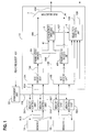
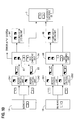
- Fig. 1 shows an example of the configuration of a dual storage apparatus in the embodiment.
- the dual storage apparatus is connected with a CPU (Central Processing Unit) through a bus not shown and executes processes in response to request signals inputted from the CPU.
- CPU Central Processing Unit
- the dual storage apparatus stores data to be written that has been inputted with the write request, into designated addresses respectively in a memory 1A and a memory 1B and notifies the CPU of the process result. In this manner, two (2) sets of identical data are stored respectively in the memory 1A and the memory 1B.
- the dual storage apparatus reads data from designated addresses and outputs data 104 including the read data to the CPU or notifies the CPU of a system error 108.
- a memory containing a plurality of storage elements for storing data is dualized (into the memory 1A and the memory 1B) and, accompanying to this, the input/output system is also dualized.
- the input/output system through which data read from the memory 1A are used is referred to as "A system” and the input/output system through which data read from the memory 1B are used is referred to as "B system” to distinguish those systems.
- a management unit 30 when a read request 101 is inputted, a management unit 30 produces an identifier (a control ID) for identifying the read request 101 and attaches the identifier to the read request 101.
- This read request attached with the control ID is outputted to a memory control unit, described later, as a memory control signal 102.
- the read request 101 contains an address designated as a read destination, a read command indicating that the process is reading (a write command when the process is writing), etc.
- the management unit 30 produces control IDs that do not include any same control IDs such that any one of the control IDs is different from others when the time at which each read request 101 to be attached with the control ID is inputted to the dual storage apparatus and the content (a designated address and commands) of the read request 101 are different, and each of the read requests is made identifiable.
- control IDs which are all different, the dual storage apparatus detects synchronization lag errors in order to process requests inputted at different times.
- a control ID is produced for a read request in the embodiment, a control ID may also be produced for a write request.
- two (2) memory control units are provided to each input/output system. That is, in the A system, a memory control unit 2A1 and a memory control unit 2A2 are provided to the memory 1A and, in the B system, a memory control unit 2B1 and a memory control unit 2B2 are provided to the memory 1B.
- the management unit 30 When the read request 101 has been inputted to the management unit 30, the management unit 30 outputs an identical memory control signal 102 respectively to four (4) memory control units.
- the memory control units 2A1 and 2A2 control the memory 1A and the memory control units 2B1 and 2B2 control the memory 2B.
- Each of the memory control units writes data to be written that is inputted with the write request, into a designated address in response to the write request issued to the memories.
- each of the memory control units outputs to the memory a designated address of the read destination plus a read command 103, and reads data 41. Then, each of the memory control units adds a header containing a control ID obtained from the memory control signal 102, to the data 41 read from the memory and provides the data with the header 104 to a data control unit 10 in a latter stage.
- the data control unit 10 comprises ECC checking units (code checking units), synchronization checking units, a coincidence checking unit 5, a selector control unit 6 and a bus selector 7.
- ECC checking units and the synchronization checking units are provided respectively to the A system and the B system.
- the ECC checking units 3A and 3B respectively executes a code check that detects uncorrectable bit errors.
- each of the ECC checking units notifies the selector control unit 6 of a code error 105.
- the synchronization checking units 4A and 4B execute respectively a synchronization check that detects synchronization errors that represent a state where the two (2) memory control units contained in each of the input/output systems are not synchronized.
- each of the synchronization checking units notifies the selector control unit 6 of the synchronization error 106.
- the synchronization checking units 4A and 4B respectively check whether or not both of the entire headers coincide and, when the headers do not coincide, a synchronization error can be determined to have occurred. In addition, when the control IDs contained respectively in the headers do not coincide, the synchronization checking units 4A and 4B may determine that a synchronization error has occurred.
- the coincidence checking unit 5 executes a coincidence check that verifies whether or not a set of data read from the memory 1A and a set of data read from the memory 1B coincide when no error has been detected by each of the synchronization checking units and each of the ECC checking units. Then, the coincidence checking unit 5 notifies the selector control unit 6 of the result 107 of the coincidence check.
- the selector control unit 6 inputs into the bus selector 7 a selection signal 108 for selecting the A system or the B system according to the check results from each of the ECC checking units and each of the synchronization checking units.
- the selector control unit 6 inputs into the bus selector 7 the selection signal 108 for selecting a system for which no error has been notified.
- the selector control unit 6 inputs into the bus selector 7 the selection signal 108 for selecting the B system.
- the selector control unit 6 inputs into the bus selector 7 the selection signal 108 for selecting the A system.
- the selector control unit 6 outputs a system error 109. Similarly, in the case where discrepancy between the two (2) sets of data has been verified in a coincidence check executed by the coincidence checking unit 5, the selector control unit 6 outputs the system error 109.
- the bus selector 7 switches the input/output system to be used.
- Fig. 1 because the content of the signals in the B system is same as that in the A system, reference numerals for the signals in the B system are omitted.
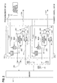
- Fig. 2 shows an example of the detailed configuration of the memory control unit in the embodiment.
- the configuration relating to the A system is shown.
- the configuration of the memory control units 2B1 and 2B2 is same as that of the memory control units 2A1 and 2A2.
- the read control signal 102 contains an address, a read command and a control ID.
- the address is information indicating the position of the data on the memory.
- the read command indicates that the signal is a read request.
- the control ID is an identifier for identifying uniquely the read request and is produced by the management unit 30.
- an address 201 is stored in address queues 11 and 21. Then, among the information contained in the read control signal 102 inputted by the management unit 30, the read command plus a control ID 202 are stored in command queues 12 and 22.
- the command queues 12 and 22 are registers that store respectively a read command and a control ID and, in response to a read request, operate synchronizing with an address that has entered the address queue 11. In the case where valid commands are stored in the command queues 12 and 22, the read commands are executed one after another to the memory 1A.
- the address queues 11 and 21 operate synchronizing with the command queues 12 and 22.
- the address stored respectively in the address queues 11 and 21 is transmitted to the memory 1A, synchronizing with the execution of the read command to the memory 1A.
- the read command plus the address 103 are inputted into the memory.
- the data 41 having been read are stored in data queues 14 and 24.
- the data queues 14 and 24 are registers that accumulate the data 41 read from the memory 1A.
- the header producing unit 13 produces a header 302 necessary for data transmission as well as executes control for keeping transmission of the header 302 waiting until the data 41 read from the memory 1A arrives. Then, the header producing unit 13 outputs a selector control signal 301 for controlling a selector 15 such that the order of the header and the data is the header plus the data. Furthermore, the header producing unit 13 manages the data queues 14 and 24 and, when the resources in the data queues 14 and 24 have depleted, outputs a BUSY signal to the command queues 12 and 22 to prevent them from outputting.
- the selector 15 Based on the selector control signal 301 inputted from the header producing unit 13, the selector 15 switches the header system and the data system such that the header plus the data are transmitted in this order. Then, the selector 15 outputs a read pointer control signal 303 to the data queue 14 in order to execute control to the data queue 14 to output necessary data. Based on the read pointer control signal from the selector 15, the data queue 14 outputs data having a necessary packet length.
- the header produced by the header producing unit 13 is attached to the set of data 41 read from the memory 1A and the data with the header 104 are inputted from the memory control unit to the data control unit in the latter stage.
- Fig. 3 shows an example of the configuration of the data with the header 104.
- the data with the header 104 are decomposed into a header 44 and the data 41.
- the header 44 is further decomposed into a header main body 45 and an ECC 46 which is a redundant code for the head main body 45.
- the control ID 203 is contained in the header main body 45.
- the data 41 are decomposed into a data main body 42 and an ECC 43 which is a redundant code for the data main body.
- An inverted bit occurring during transmission is detected by the ECC 46 for the header and the ECC 43 for the data.
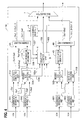
- Fig. 4 shows an example of the detailed configuration of the data control unit 10 in the embodiment.
- ECC checking units 3A and 3B shown in Fig. 1 four (4) (HD separating units 8A1, 8A2, 8B1 and 8B2) header/data separating units (HD separating units) in total for decomposing the data with the header 104 to be inputted into the data control unit 10 into the header 44 and the data 41 are provided.
- HDMI separating units 8A1, 8A2, 8B1 and 8B2 header/data separating units
- the ECC checking units 3A and 3B shown in Fig. 1 are divided into data ECC checking units 31A and 31B that check the ECC 43 of the data and header ECC checking units 32A and 32B that check the ECC 46 of the header. Then, at a stage after the synchronization checking units 4A and 4B, combining units 9A and 9B for re-combining the header 44 and the data 41 that have once been once separated are provided. The above points have been made more detailed than those of Fig. 1.
- the HD separating unit 8A1 separates the data with the header 104 inputted from the memory control unit 2A1, into a header Ha1 and data Da1.
- the HD separating unit 8A2 separates the data with the header 104 inputted from the memory control unit 2A2 into a header Ha2 and data Da2. Then, the data Da1 and Da2 are inputted into the data ECC checking unit 31A and the headers ha1 and ha2 are inputted into the header ECC checking unit 32A.
- the data ECC checking unit 31A Having detected an uncorrectable bit error in either of the data Da1 and Da2, the data ECC checking unit 31A inputs a code error 105d relating to the data into the selector control unit 6. Having detected an uncorrectable bit error in either of the headers Ha1 and Ha2, the header ECC checking unit 32A inputs a code error 105h relating to the header into the selector control unit 6.
- the header ECC checking unit 32A inputs the headers Ha1 and Ha2 into the synchronization checking unit 4A. Having detected a synchronization error based on the control ID contained in the header, the synchronization checking unit 4A notifies the selector control unit 6 of the synchronization error 106.
- the combining units 9A and 9B recombine the header 44 and the data 41 that have been separated, and input the combined header 44 and the data 41 into the bus selector 7.
- the combining units 9A and 9B input the data 41 into the coincidence checking unit 5.
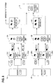
- Fig. 5 is a flowchart describing the operation of the selector control unit 6 in the embodiment.
- the selector control unit 6 determines whether or not any data ECC error has occurred (S1). If the code error 105d relating to the data has been inputted by the data ECC checking units 31A and 31B, the selector control unit 6 determines that a data ECC error has occurred. In this case, to which system the error has occurred is also notified to the selector control unit 6.
- the selector control unit 6 determines whether or not any header ECC error has occurred (S2) . If the code error 105h relating to the header has been inputted by the header ECC checking units 32A and 32B, the selector control unit 6 determines that a header ECC error has occurred. In this case, to which system the error has occurred is also notified to the selector control unit 6.
- the selector control unit 6 determines whether or not any synchronization error has occurred (S3). If the synchronization error 106 has been inputted by the synchronization checking units 4A and 4B, the selector control unit 6 determines that a synchronization error has occurred. In this case, to which system the error has occurred is also notified to the selector control unit 6.
- the selector control unit 6 determines whether or not the sets of data read from the memory 1A and memory 1B coincide (S4) . If the sets of data from both of the systems coincide (S4 Yes), the set of data from either system may be used and, in this case, the selector control unit 6 outputs a selection signal that controls the selector such that the set of data read from the memory 1A is used (S8) . In this case, the selector may be controlled such that the set of data read from the memory 1A is used.
- the selector control unit 6 determines whether or not the system to which the error has been detected is the A system (S5) . In the case where the error has been detected in the B system (S5 No), the selector control unit 6 outputs a selection signal that controls the selector such that the set of data read from the memory 1A is used (S8).
- the selector control unit 6 determines whether or not the error has been detected also in the B system (S6). In the case where no error has been detected in the B system (S6 No), the selector control unit 6 outputs a selection signal that controls the selector such that the set of data read from the memory 1B is used (S9).
- the selector control unit 6 In the case where an error has been detected in both of the A system and the B system (S6 Yes), the selector control unit 6 outputs the system error (S7).
- S7 system error
- Fig. 7 is an explanatory view of the normal operation of the dual storage apparatus in the embodiment.
- the data 41 read from the memory 1A are inputted into the memory control units 2A1 and 2A2.
- the memory control units 2A1 and 2A2 attach identical headers respectively to the inputted data and input the data with the header 104 into the ECC checking unit 3A.
- the ECC checking unit 3A executes a code check on the header and the data. In this check, no error is detected.
- the ECC checking unit 3A inputs the header into the synchronization checking unit 4A.
- synchronization checking unit 4A In the synchronization checking unit 4A, a synchronization check on the header is executed. Similarly, in this check, no error is detected. This process is also executed for the B system. A code check is executed in the ECC checking unit 3B and a synchronization check is executed in the synchronization checking unit 4B. Similarly, in these checks, no error is detected.
- the selector control unit 6 controls the bus selector 7 such that, for example, the set of data read from the memory 1A is used.
- Fig. 8 is an explanatory view of an example of the case where the dual storage apparatus detects an error in one system in a synchronization check.
- the set of data 41 read from the memory 1A are inputted into the memory control units 2A1 and 2A2.
- a synchronization lag has occurred between the memory control units 2A1 and 2A2 and a different header 81 is attached in the memory control unit 2A2.
- a code check is executed on the header and the data in the ECC checking unit 3A. In this check, no error is detected. This is because no inverted bit (bit invert) during the transmission has occurred and no ECC error is detected though the headers accompany the synchronization lag between them.
- ECC checking unit 3A inputs the header into the synchronization checking unit 4A.
- a synchronization check on the header is executed in the synchronization checking unit 4A. In this check, a synchronization error is detected. Then, the synchronization checking unit 4A notifies the selector control unit 6 that a synchronization error has been detected in the A system.
- a same process is also executed for the B system.
- a code check is executed in the ECC checking unit 3B and a synchronization check is executed in the synchronization checking unit 4B.
- the selector control unit 6 controls the bus selector 7 such that the set of data read from the memory 1B is used.
- Fig. 9 is an explanatory view of an example of the case where the dual storage apparatus detects errors in both of the systems in synchronization checks.
- the set of data 41 read from the memory 1A are inputted into the memory control units 2A1 and 2A2.
- a synchronization lag has occurred between the memory control units 2A1 and 2A2, and a different header 81 is attached by the memory control unit 2A2.
- a synchronizationlag has occurred between the memory control units 2B1 and 2B2, and the different header 81 is attached by the memory control unit 2B1.
- a code check is executed on the header and the data in the ECC checking unit 3A. In this check, no error is detected. This is because no bit inversion during the transmission has occurred and no ECC error is detected though the headers accompany the synchronization lag between them.
- the ECC checking unit 3A inputs the header into the synchronization checking unit 4A.
- a synchronization check on the header is executed in the synchronization checking unit 4A. In this check, a synchronization error is detected.
- the synchronization checking unit 4A notifies the selector control unit 6 that a synchronization error has been detected in the A system.
- a same process is also executed for the B system.
- a code check is executed in the ECC checking unit 3B and a synchronization check is executed in the synchronization checking unit 4B.
- a synchronization error is detected by the synchronization checking unit 4B.
- the synchronization checking unit 4B notifies the selector control unit 6 that a synchronization error has been detected in the B system.
- the selector control unit 6 notifies of a system error because an error has been detected respectively in both of the A system and the B system.
- Fig. 10 is an explanatory view of an example of the case where the dual storage apparatus detects an error in one system in an ECC check on the headers.
- the set of data 41 read from the memory 1A is inputted into the memory control units 2A1 and 2A2.
- the memory control units 2A1 and 2A2 attach identical headers respectively to the inputted set of data and input the set of data with the header 104 into the ECC checking unit 3A.
- a bit invert occurs in the header outputted from the memory control unit 2A2 in the course of the transmission to the ECC checking unit 3A (in Fig. 10, a header 82 to which a bit invert has occurred is depicted as a shape that can not form a square even when the header and the ECC are coupled together).
- a code check on the header and the data is executed in the ECC checking unit 3A.
- a code error relating to the header is detected.
- the ECC checking unit 3A notifies the selector control unit 6 that a synchronization error has been detected in the A system.
- a same process is also executed for the B system.
- a code check is executed in the ECC checking unit 3B and a synchronization check is executed in the synchronization checking unit 4B. No error is detected in the B system.
- the selector control unit 6 controls the bus selector 7 such that the set of data read from the memory 1B is used.
- Fig. 11 is an explanatory view of an example of the case where the dual storage apparatus detects an error in one system in an ECC check on the data.
- the set of data 41 read from the memory 1A are inputted into the memory control units 2A1 and 2A2.
- the memory control units 2A1 and 2A2 attach an identical header respectively to the inputted set of data and input the set of data with the header 104 into the ECC checking unit 3A.
- a bit inversion occurs in data outputted from the memory control unit 2A2 in the course of transmission to the ECC checking unit 3A (in Fig. 11.
- a set of data 83 to which a bit inversion occurred is depicted as a shape formed by adding a semicircle painted black to a shape indicating the set of data 41 that has been read) .
- a code check on the header and the data is executed in the ECC checking unit 3A. In this check, a code error relating to the data is detected. Then, the ECC checking unit 3A notifies the selector control unit 6 that a synchronization error has been detected in the A system.
- a same process is also executed for the B system.
- a code check is executed in the ECC checking unit 3B and a synchronization check is executed in the synchronization checking unit 4B. No error is detected in the B system.
- the selector control unit 6 controls the bus selector 7 such that the set of data read from the memory 1B is used.
- Fig. 12 is an explanatory view of an example of the case where the dual storage apparatus detects errors in both of the systems in synchronization checks on the data.
- the set of data 41 read from the memory 1A is inputted into the memory control units 2A1 and 2A2.
- the memory control units 2A1 and 2A2 attach an identical header respectively to the inputted set of data and input the set of data with the header 104 into the ECC checking unit 3A.
- a bit invert occurs to the data outputted from the memory control unit 2A2 in the course of transmission to the ECC checking unit 3A (in Fig. 12, the set of data 83 to which a bit invert has occurred is depicted as a shape formed by attaching a semicircle painted black to a shape indicating the set of data 41 that has been read).
- a bit invert occurs to a set of data outputted from the memory control unit 2B1 in the course of transmission to the ECC checking unit 3B.
- a code check is executed on the header and the data in the ECC checking unit 3A. In this check, a code error relating to the data is detected. Then, the ECC checking unit 3A notifies the selector control unit 6 that a synchronization error has been detected in the A system.
- a same process is also executed for the B system and a code error relating to the set of data is detected by the ECC checking unit 3B. Then, the ECC checking unit 3B notifies the selector control unit 6 that a synchronization error has been detected in the B system.
- the selector control unit 6 notifies of a system error because an error has been detected respectively in both of the A system and the B system.
- Fig. 13 is an explanatory view of an example of the case where the dual storage apparatus detects an error in a coincidence check on the data. This shows the case of multiple defects where the set of data read from the memory 1A and the set of data read from the memory 1B are different from each other though no error is detected in a code check and a synchronization check.
- the set of data 41 read from the memory 1A is inputted into the memory control units 2A1 and 2A2.
- the memory control units 2A1 and 2A2 attach an identical header respectively to the inputted sets of data and input the sets of data with the header 104 into the ECC checking unit 3A.
- a code check on the headers and the data is executed in the ECC checking unit 3A. In this check, no error is detected.
- the ECC checking unit 3A inputs the headers into the synchronization checking unit 4A. In the synchronization checking unit 4A, a synchronization check on the headers is executed. Similarly, in this check, no error is detected.
- This process is also executed for the B system.
- a code check is executed in the ECC checking unit 3B and a synchronization check is executed in the synchronization checking unit 4B. Similarly, in these checks, no error is detected.
- the set of data read from the memory 1A and the set of data read from the memory 1B are inputted into the coincidence checking unit 5 and a coincidence check is executed on them. Then, discrepancy between the two (2) sets of data can be verified first by the coincidence check. In this case, the selector control unit 6 can not determine which set of data should be used and, therefore, outputs a system error.
- the dual storage apparatus may be adapted to divide the data read from the memory into two (2) and input the divided data respectively into the memory control unit of each of the input/output systems.
- the dual storage apparatus may be adapted to divide 72-bit data (64 bits of a data portion plus eight (8) bits of an ECC portion) into two (2) sets of 36-bit data (32 bits of a data portion plus four (4) bits of an ECC portion) and input the former set into the memory control unit 2A1 and the latter set into the memory control unit 2A2.
- the occurrence of malfunction which is conventionally the cause for stopping a computer and degrading the reliability of the computer can be precluded, and continuous operation of the computer is further enabled without degrading the reliability demanded for the computer.
- the phenomena affecting computers that use dual storage apparatuses such as wrong timing of data, loss of data, wrong order of data, etc. can be precluded. foregoing can be summarized as the following claims.
Abstract
Description
- The present invention relates to a dual storage apparatus which includes a memory for retaining data and an input/output system for the memory, both of which are dualized to improve reliability, and to a control method for the dual storage apparatus.
- Currently, the scope within which computers are needed industrially has been expanded and improved reliability is demanded for the computers. One type of reliability that is demanded for a computer is fault tolerance that guarantees that the computer can operate continuously even when a resource used in the computer (such as a CPU (Central Processing Unit), a memory, a hard disk, etc) has become defective, and another one is error tolerance that is an ability to be able to detect and correct a data error, e.g. a bit inversion generated in the course of transmission of information.
- As one of the methods of improving the reliability demanded for a computer, multiplexing of the resources can be listed. For example, according to
Japanese Patent Application Laid-Open Publication Nos. 1987-140153 1992-149653 1982-101950 1996-297588 - Therefore, the fault tolerance can be improved because, even when one (1) counterpart memory has become defective, the data stored in the other counterpart memory can be used. In addition, because the data can not be used until the two (2) sets of data read from the dual memory coincide, detection/correction of errors in the data are executed during the comparison, thereby, the error tolerance can be improved.
- A memory is controlled by a memory controller that processes read requests and write requests issued to the memory. In recent years, an LSI (Large Scale Integration) used in this memory controller has a complicated configuration due to the increase in capacity of a DIMM (Dual Inline Memory Module) and growth in speed of data transfer. Therefore, the possibility that errors occur in the LSI and the possibility that the LSI is affected by the exterior environment through, for example, disturbance have become high.
- When memories are dualized, the input/output system for each of the memories is also dualized and a memory controller is provided to each counterpart input/output system. Then, in general, two (2) memory controllers operate symmetrically (i. e., are synchronized). However, the controllers provided respectively to the counterpart input/output systems may operate differently from each other because of errors having occurred internally or disturbance even though the LSIs are those that operate symmetrically (i. e., being synchronized) under completely like conditions.
- When the operation of the counterpart memory controllers in the dual memory becomes asymmetrical (not synchronized), phenomena such as, for example, a timing lag between the sets of data, loss of data, wrong order of data may occur in the computer. For example, when the data have been read, the two (2) sets of data read from the counterpart memories do not coincide only because of a timing lag between the sets of data. In this case, both sets of data themselves have not been destroyed, however, the computer can not determine which set of data should be used for processing. Therefore, continuous operation of the computer becomes impossible.
- As described above, the prior art has a problem that, even when a memory is dualized, the operation of the computer is required to stop due to the malfunction of an LSI used in the memory controller and, then, the continuous operation of the computer becomes impossible even when the memory is dualized, therefore, the reliability demanded for the computer is degraded.
- It is therefore desirable to provide a dual storage apparatus which enables further the continuous operation of a computer without degrading the reliability demanded for the computer, and a control method for the dual storage apparatus.
- According to a first aspect of the present invention there is provided a dual storage apparatus including first and second memories for respectively retaining a set of identical data, and a selector for selecting either of the two sets of data read from the first and the second memories based on a read control signal inputted into the selector, wherein the dual storage apparatus comprises a request management unit for, when the read control signal has been inputted, attaching an identifier for identifying the read control signal to the inputted read control signal and outputting the signal and the identifier; a first main memory control unit for reading the data from the first memory based on the read control signal outputted from the request management unit, and outputting a set of data read from the first memory with the identifier attached to the read control signal outputted from the request management unit; a first sub memory control unit for inputting the read control signal outputted from the request management unit and the data read by the first main memory control unit, and outputting the inputted data with the identifier attached to the read control signal outputted from the request management unit; a second main memory control unit for reading the data from the second memory based on the read control signal outputted from the request management unit, and outputting a set of data read from the second memory with the identifier attached to the read control signal outputted from the request management unit; a second sub memory control unit for inputting the read control signal outputted from the request management unit and the data read by the second main memory control unit, and outputting the inputted data with the identifier attached to the read control signal outputted from the request management unit; a synchronization checking unit for verifying coincidence of the identifiers inputted from the first memory control unit and the first sub memory control unit, and coincidence of the identifiers inputted from the second main memory control unit and the second sub memory control unit; and a selector control unit for controlling the selector based on the result of the verification.
- Preferably, the dual storage apparatus further comprises a coincidence checking unit for verifying whether or not the set of data read from the first memory and the set of data read from the second memory coincide when coincidence of the identifiers inputted from the first main memory control unit and the first sub memory control unit and coincidence of the identifiers inputted from the second main memory control unit and the second sub memory control unit have been both verified, and wherein the selector control unit outputs a system error when the coincidence has not been verified by the coincidence checking unit. Preferably, when coincidence of the identifiers inputted from the first main memory control unit and the first sub memory control unit has been verified, the selector control unit controls the selector such that the set of data read from the first memory is selected, and, when the coincidence of the identifiers inputted from the first main memory control unit and the first sub memory control unit has not been verified and coincidence of the identifiers inputted from the second main memory control unit and the second sub memory control unit has been verified, controls the selector such that the set of data read from the second memory is selected. Preferably, the selector control unit outputs a system error when coincidence of the identifier inputted from the first main memory control unit and the first sub memory control unit and coincidence of the identifier inputted from the second main memory control unit and the second sub memory control unit have not been both verified by the synchronization checking unit. Preferably, the dual storage apparatus further has a code checking unit for checking an error detection/correction code attached to each set of the data, and wherein, when no uncorrectable error has been detected in either set of data read from the first memory by the code checking unit, the selector control unit controls the selector such that the set of data read from the first memory is selected; and, when an uncorrectable error has been detected in either set of data read from the first memory and no uncorrectable error has been detected in either set of data read from the second memory, controls the selector such that the set of data read from the second memory are selected. Preferably, the selector control unit outputs a system error when an uncorrectable error has been detected in either set of data read from the first memory and an uncorrectable error has been detected in either set of data read from the second memory, by the code checking unit.
- According to a second aspect of the present invention there is provided a controlling method for a dual storage apparatus comprising a first and a second memories for respectively retaining a set of identical data and a selector for selecting either of the two sets of data read from the first and the second memories based on a read control signal inputted into the selector, wherein the dual storage apparatus produces an identifier for identifying the read control signal when the read control signal has been inputted, wherein the dual storage apparatus produces first main data by reading the data from the first memory based on the read control signal and adding the identifier attached to the read control signal, to the data read from the first memory, wherein the dual storage apparatus produces first sub data by adding the identifier attached to the read control signal, to the data read from the first memory, wherein the dual storage apparatus produces second main data by reading the data from the second memory based on the read control signal and adding the identifier attached to the read control signal, to the data read from the second memory, wherein the dual storage apparatus produces second sub data by adding the identifier attached to the read control signal, to the data read from the second memory, wherein the dual storage apparatus verifies coincidence of the identifiers respectively contained in the first main data and the first sub data and coincidence of the identifiers respectively contained in the second main data and the second sub data, and wherein the dual storage apparatus controls the selector based on the result of the verification.
- Using the dual storage apparatus of an embodiment of the present invention, the continuous operation of a computer can be enabled further without degrading the reliability demanded for the computer.
- The above and othe features and advantages of the present invention will become more apparent from the following detailed description when taken in conjunction with the accompanying drawings, in which:
- Fig. 1 shows an example of the configuration of a dual storage apparatus in the embodiment;
- Fig. 2 shows an example of the detailed configuration of the memory control unit in the embodiment;
- Fig. 3 shows an example of the configuration of the data with the header;
- Fig. 4 shows an example of the detailed configuration of the data control unit in the embodiment;
- Fig. 5 is a flowchart describing the operation of the selector control unit in the embodiment;
- Fig. 6 is a table describing summarized operation of the dual storage apparatus in the embodiment;
- Fig. 7 is an explanatory view of the normal operation of the dual storage apparatus in the embodiment;
- Fig. 8 is an explanatory view of an example of the case where the dual storage apparatus detects an error in one system in a synchronization check;
- Fig. 9 is an explanatory view of an example of the case where the dual storage apparatus detects errors in both of the systems in synchronization checks;
- Fig. 10 is an explanatory view of an example of the case where the dual storage apparatus detects an error in one system in an ECC check on the headers;
- Fig. 11 is an explanatory view of an example of the case where the dual storage apparatus detects an error in one system in an ECC check on the data;
- Fig. 12 is an explanatory view of an example of the case where the dual storage apparatus detects errors in both of the systems in synchronization checks on the data; and
- Fig. 13 is an explanatory view of an example of the case where the dual storage apparatus detects an error in a coincidence check on the data.
- An embodiment of the present invention will now be described with reference to the accompanying drawings. It is however to be noted that the technical scope of the present invention is not limited to the embodiment but covers the invention as defined in the appended claims and equivalents thereof.
- Fig. 1 shows an example of the configuration of a dual storage apparatus in the embodiment. The dual storage apparatus is connected with a CPU (Central Processing Unit) through a bus not shown and executes processes in response to request signals inputted from the CPU.
- For example, in case of a write request, the dual storage apparatus stores data to be written that has been inputted with the write request, into designated addresses respectively in a
memory 1A and amemory 1B and notifies the CPU of the process result. In this manner, two (2) sets of identical data are stored respectively in thememory 1A and thememory 1B. When the request is aread request 101, the dual storage apparatus reads data from designated addresses and outputsdata 104 including the read data to the CPU or notifies the CPU of asystem error 108. - In the dual storage apparatus of the embodiment, a memory containing a plurality of storage elements for storing data is dualized (into the
memory 1A and thememory 1B) and, accompanying to this, the input/output system is also dualized. Herein, the input/output system through which data read from thememory 1A are used is referred to as "A system" and the input/output system through which data read from thememory 1B are used is referred to as "B system" to distinguish those systems. - As a feature of the dual storage apparatus of the embodiment, when a
read request 101 is inputted, amanagement unit 30 produces an identifier (a control ID) for identifying theread request 101 and attaches the identifier to theread request 101. This read request attached with the control ID is outputted to a memory control unit, described later, as amemory control signal 102. - The
read request 101 contains an address designated as a read destination, a read command indicating that the process is reading (a write command when the process is writing), etc. Themanagement unit 30 produces control IDs that do not include any same control IDs such that any one of the control IDs is different from others when the time at which each readrequest 101 to be attached with the control ID is inputted to the dual storage apparatus and the content (a designated address and commands) of theread request 101 are different, and each of the read requests is made identifiable. - Using these control IDs which are all different, the dual storage apparatus detects synchronization lag errors in order to process requests inputted at different times. Though a control ID is produced for a read request in the embodiment, a control ID may also be produced for a write request.
- Furthermore, as another feature of the dual storage apparatus of the embodiment, two (2) memory control units are provided to each input/output system. That is, in the A system, a memory control unit 2A1 and a memory control unit 2A2 are provided to the
memory 1A and, in the B system, a memory control unit 2B1 and a memory control unit 2B2 are provided to thememory 1B. When theread request 101 has been inputted to themanagement unit 30, themanagement unit 30 outputs an identicalmemory control signal 102 respectively to four (4) memory control units. - The memory control units 2A1 and 2A2 control the
memory 1A and the memory control units 2B1 and 2B2 control thememory 2B. Each of the memory control units writes data to be written that is inputted with the write request, into a designated address in response to the write request issued to the memories. - In addition, in response to the
read request 101 issued to the memories, each of the memory control units outputs to the memory a designated address of the read destination plus aread command 103, and readsdata 41. Then, each of the memory control units adds a header containing a control ID obtained from thememory control signal 102, to thedata 41 read from the memory and provides the data with theheader 104 to adata control unit 10 in a latter stage. - The
data control unit 10 comprises ECC checking units (code checking units), synchronization checking units, acoincidence checking unit 5, aselector control unit 6 and abus selector 7. The ECC checking units and the synchronization checking units are provided respectively to the A system and the B system. - Based on an Error Checking and Correct Code (ECC) contained respectively in the header and the data included in the data with the
header 104, theECC checking units selector control unit 6 of acode error 105. - Based on the control ID contained in the header included in the data with the
header 104, thesynchronization checking units selector control unit 6 of thesynchronization error 106. - The
synchronization checking units synchronization checking units - In order to detect a multiple defect that can not be detected by each of the synchronization checking units and each of the ECC checking units, the
coincidence checking unit 5 executes a coincidence check that verifies whether or not a set of data read from thememory 1A and a set of data read from thememory 1B coincide when no error has been detected by each of the synchronization checking units and each of the ECC checking units. Then, thecoincidence checking unit 5 notifies theselector control unit 6 of theresult 107 of the coincidence check. - The
selector control unit 6 inputs into the bus selector 7 aselection signal 108 for selecting the A system or the B system according to the check results from each of the ECC checking units and each of the synchronization checking units. Theselector control unit 6 inputs into thebus selector 7 theselection signal 108 for selecting a system for which no error has been notified. - For example, in the case where the
ECC checking unit 3A notifies of thecode error 105, theselector control unit 6 inputs into thebus selector 7 theselection signal 108 for selecting the B system. In the case where thesynchronization checking unit 4B notifies of asynchronization error 106, theselector control unit 6 inputs into thebus selector 7 theselection signal 108 for selecting the A system. - Then, in the case where an error is notified respectively from both of the systems, the
selector control unit 6 outputs asystem error 109. Similarly, in the case where discrepancy between the two (2) sets of data has been verified in a coincidence check executed by thecoincidence checking unit 5, theselector control unit 6 outputs thesystem error 109. - Based on the selection signal from the
selector control unit 6, thebus selector 7 switches the input/output system to be used. In Fig. 1, because the content of the signals in the B system is same as that in the A system, reference numerals for the signals in the B system are omitted. - Fig. 2 shows an example of the detailed configuration of the memory control unit in the embodiment. In Fig. 2, the configuration relating to the A system is shown. However, the configuration of the memory control units 2B1 and 2B2 is same as that of the memory control units 2A1 and 2A2.
- The read control signal 102 contains an address, a read command and a control ID. The address is information indicating the position of the data on the memory. The read command indicates that the signal is a read request. The control ID is an identifier for identifying uniquely the read request and is produced by the
management unit 30. - Among the information contained in the read control signal 102 inputted by the
management unit 30, anaddress 201 is stored inaddress queues management unit 30, the read command plus acontrol ID 202 are stored incommand queues - The
command queues address queue 11. In the case where valid commands are stored in thecommand queues memory 1A. - When a command is executed, information necessary for producing a header is outputted from the
command queue 12 to a producingunit 13. Acontrol ID 203 is contained in this information. - The
address queues command queues address queues memory 1A, synchronizing with the execution of the read command to thememory 1A. - In this manner, the read command plus the
address 103 are inputted into the memory. Then, thedata 41 having been read are stored indata queues data queues data 41 read from thememory 1A. - The
header producing unit 13 produces aheader 302 necessary for data transmission as well as executes control for keeping transmission of theheader 302 waiting until thedata 41 read from thememory 1A arrives. Then, theheader producing unit 13 outputs aselector control signal 301 for controlling aselector 15 such that the order of the header and the data is the header plus the data. Furthermore, theheader producing unit 13 manages thedata queues data queues command queues - Based on the
selector control signal 301 inputted from theheader producing unit 13, theselector 15 switches the header system and the data system such that the header plus the data are transmitted in this order. Then, theselector 15 outputs a readpointer control signal 303 to thedata queue 14 in order to execute control to thedata queue 14 to output necessary data. Based on the read pointer control signal from theselector 15, thedata queue 14 outputs data having a necessary packet length. - In this manner, the header produced by the
header producing unit 13 is attached to the set ofdata 41 read from thememory 1A and the data with theheader 104 are inputted from the memory control unit to the data control unit in the latter stage. - Fig. 3 shows an example of the configuration of the data with the
header 104. The data with theheader 104 are decomposed into aheader 44 and thedata 41. Among these, theheader 44 is further decomposed into a headermain body 45 and anECC 46 which is a redundant code for the headmain body 45. Thecontrol ID 203 is contained in the headermain body 45. - Furthermore, the
data 41 are decomposed into a datamain body 42 and anECC 43 which is a redundant code for the data main body. An inverted bit occurring during transmission is detected by theECC 46 for the header and theECC 43 for the data. - Fig. 4 shows an example of the detailed configuration of the
data control unit 10 in the embodiment. At a stage before theECC checking units header 104 to be inputted into thedata control unit 10 into theheader 44 and thedata 41 are provided. - The
ECC checking units ECC checking units ECC 43 of the data and headerECC checking units ECC 46 of the header. Then, at a stage after thesynchronization checking units units header 44 and thedata 41 that have once been once separated are provided. The above points have been made more detailed than those of Fig. 1. - The HD separating unit 8A1 separates the data with the
header 104 inputted from the memory control unit 2A1, into a header Ha1 and data Da1. Similarly, the HD separating unit 8A2 separates the data with theheader 104 inputted from the memory control unit 2A2 into a header Ha2 and data Da2. Then, the data Da1 and Da2 are inputted into the dataECC checking unit 31A and the headers ha1 and ha2 are inputted into the headerECC checking unit 32A. - Having detected an uncorrectable bit error in either of the data Da1 and Da2, the data
ECC checking unit 31A inputs acode error 105d relating to the data into theselector control unit 6. Having detected an uncorrectable bit error in either of the headers Ha1 and Ha2, the headerECC checking unit 32A inputs acode error 105h relating to the header into theselector control unit 6. - Then, the header
ECC checking unit 32A inputs the headers Ha1 and Ha2 into thesynchronization checking unit 4A. Having detected a synchronization error based on the control ID contained in the header, thesynchronization checking unit 4A notifies theselector control unit 6 of thesynchronization error 106. - The combining
units header 44 and thedata 41 that have been separated, and input the combinedheader 44 and thedata 41 into thebus selector 7. The combiningunits data 41 into thecoincidence checking unit 5. - The description for the remaining portions is same as that in Fig. 1 and, therefore, is omitted.
- Fig. 5 is a flowchart describing the operation of the
selector control unit 6 in the embodiment. First, theselector control unit 6 determines whether or not any data ECC error has occurred (S1). If thecode error 105d relating to the data has been inputted by the dataECC checking units selector control unit 6 determines that a data ECC error has occurred. In this case, to which system the error has occurred is also notified to theselector control unit 6. - In the case where no data ECC error has occurred (S1 No), the
selector control unit 6 determines whether or not any header ECC error has occurred (S2) . If thecode error 105h relating to the header has been inputted by the headerECC checking units selector control unit 6 determines that a header ECC error has occurred. In this case, to which system the error has occurred is also notified to theselector control unit 6. - In the case where no header ECC error has occurred (S2 No), the
selector control unit 6 determines whether or not any synchronization error has occurred (S3). If thesynchronization error 106 has been inputted by thesynchronization checking units selector control unit 6 determines that a synchronization error has occurred. In this case, to which system the error has occurred is also notified to theselector control unit 6. - In the case where no error has been detected by the code check and the synchronization check (S3 No), the
selector control unit 6 determines whether or not the sets of data read from thememory 1A andmemory 1B coincide (S4) . If the sets of data from both of the systems coincide (S4 Yes), the set of data from either system may be used and, in this case, theselector control unit 6 outputs a selection signal that controls the selector such that the set of data read from thememory 1A is used (S8) . In this case, the selector may be controlled such that the set of data read from thememory 1A is used. - In the case where no error has been detected by the code check and the synchronization check, however, the sets of data from both systems do not coincide (S4 No), which set of data should be used can not be determined and the
selector control unit 6 outputs the system error (S7). - In the case where an error has been detected by the code check and the synchronization check (S1 Yes, S2 Yes and S3 Yes), the
selector control unit 6 determines whether or not the system to which the error has been detected is the A system (S5) . In the case where the error has been detected in the B system (S5 No), theselector control unit 6 outputs a selection signal that controls the selector such that the set of data read from thememory 1A is used (S8). - In the case where an error has been detected in the A system (S5 Yes), the
selector control unit 6 determines whether or not the error has been detected also in the B system (S6). In the case where no error has been detected in the B system (S6 No), theselector control unit 6 outputs a selection signal that controls the selector such that the set of data read from thememory 1B is used (S9). - In the case where an error has been detected in both of the A system and the B system (S6 Yes), the
selector control unit 6 outputs the system error (S7). The operation of Fig. 5 described above is summarized in the table of Fig. 6. - The operation will be described as follows referring to a detailed example.
- Fig. 7 is an explanatory view of the normal operation of the dual storage apparatus in the embodiment. The
data 41 read from thememory 1A are inputted into the memory control units 2A1 and 2A2. The memory control units 2A1 and 2A2 attach identical headers respectively to the inputted data and input the data with theheader 104 into theECC checking unit 3A. - The
ECC checking unit 3A executes a code check on the header and the data. In this check, no error is detected. TheECC checking unit 3A inputs the header into thesynchronization checking unit 4A. - In the
synchronization checking unit 4A, a synchronization check on the header is executed. Similarly, in this check, no error is detected. This process is also executed for the B system. A code check is executed in theECC checking unit 3B and a synchronization check is executed in thesynchronization checking unit 4B. Similarly, in these checks, no error is detected. - Finally, the set of data read from the
memory 1A and the set of data read from thememory 1B are inputted into thecoincidence checking unit 5 and a coincidence check is executed. Then, based on the fact that no error has been detected, theselector control unit 6 controls thebus selector 7 such that, for example, the set of data read from thememory 1A is used. - Fig. 8 is an explanatory view of an example of the case where the dual storage apparatus detects an error in one system in a synchronization check. The set of
data 41 read from thememory 1A are inputted into the memory control units 2A1 and 2A2. In Fig. 8, a synchronization lag has occurred between the memory control units 2A1 and 2A2 and adifferent header 81 is attached in the memory control unit 2A2. - A code check is executed on the header and the data in the
ECC checking unit 3A. In this check, no error is detected. This is because no inverted bit (bit invert) during the transmission has occurred and no ECC error is detected though the headers accompany the synchronization lag between them. - Then
ECC checking unit 3A inputs the header into thesynchronization checking unit 4A. A synchronization check on the header is executed in thesynchronization checking unit 4A. In this check, a synchronization error is detected. Then, thesynchronization checking unit 4A notifies theselector control unit 6 that a synchronization error has been detected in the A system. - A same process is also executed for the B system. A code check is executed in the
ECC checking unit 3B and a synchronization check is executed in thesynchronization checking unit 4B. In the B system, no error is detected. Finally, theselector control unit 6 controls thebus selector 7 such that the set of data read from thememory 1B is used. - Fig. 9 is an explanatory view of an example of the case where the dual storage apparatus detects errors in both of the systems in synchronization checks. The set of
data 41 read from thememory 1A are inputted into the memory control units 2A1 and 2A2. In Fig. 8, a synchronization lag has occurred between the memory control units 2A1 and 2A2, and adifferent header 81 is attached by the memory control unit 2A2. In addition, a synchronizationlag has occurred between the memory control units 2B1 and 2B2, and thedifferent header 81 is attached by the memory control unit 2B1. - A code check is executed on the header and the data in the
ECC checking unit 3A. In this check, no error is detected. This is because no bit inversion during the transmission has occurred and no ECC error is detected though the headers accompany the synchronization lag between them. - Then, the
ECC checking unit 3A inputs the header into thesynchronization checking unit 4A. A synchronization check on the header is executed in thesynchronization checking unit 4A. In this check, a synchronization error is detected. Then, thesynchronization checking unit 4A notifies theselector control unit 6 that a synchronization error has been detected in the A system. - A same process is also executed for the B system. A code check is executed in the
ECC checking unit 3B and a synchronization check is executed in thesynchronization checking unit 4B. As a result, a synchronization error is detected by thesynchronization checking unit 4B. Then, thesynchronization checking unit 4B notifies theselector control unit 6 that a synchronization error has been detected in the B system. - In this case, the
selector control unit 6 notifies of a system error because an error has been detected respectively in both of the A system and the B system. - Fig. 10 is an explanatory view of an example of the case where the dual storage apparatus detects an error in one system in an ECC check on the headers. The set of
data 41 read from thememory 1A is inputted into the memory control units 2A1 and 2A2. The memory control units 2A1 and 2A2 attach identical headers respectively to the inputted set of data and input the set of data with theheader 104 into theECC checking unit 3A. In Fig. 8, it is assumed that a bit invert occurs in the header outputted from the memory control unit 2A2 in the course of the transmission to theECC checking unit 3A (in Fig. 10, aheader 82 to which a bit invert has occurred is depicted as a shape that can not form a square even when the header and the ECC are coupled together). - A code check on the header and the data is executed in the
ECC checking unit 3A. In this check, a code error relating to the header is detected. Then, theECC checking unit 3A notifies theselector control unit 6 that a synchronization error has been detected in the A system. - A same process is also executed for the B system. A code check is executed in the
ECC checking unit 3B and a synchronization check is executed in thesynchronization checking unit 4B. No error is detected in the B system. Finally, theselector control unit 6 controls thebus selector 7 such that the set of data read from thememory 1B is used. - Fig. 11 is an explanatory view of an example of the case where the dual storage apparatus detects an error in one system in an ECC check on the data. The set of
data 41 read from thememory 1A are inputted into the memory control units 2A1 and 2A2. The memory control units 2A1 and 2A2 attach an identical header respectively to the inputted set of data and input the set of data with theheader 104 into theECC checking unit 3A. In Fig. 11, it is assumed that a bit inversion occurs in data outputted from the memory control unit 2A2 in the course of transmission to theECC checking unit 3A (in Fig. 11. a set ofdata 83 to which a bit inversion occurred is depicted as a shape formed by adding a semicircle painted black to a shape indicating the set ofdata 41 that has been read) . A code check on the header and the data is executed in theECC checking unit 3A. In this check, a code error relating to the data is detected. Then, theECC checking unit 3A notifies theselector control unit 6 that a synchronization error has been detected in the A system. - A same process is also executed for the B system. A code check is executed in the
ECC checking unit 3B and a synchronization check is executed in thesynchronization checking unit 4B. No error is detected in the B system. Finally, theselector control unit 6 controls thebus selector 7 such that the set of data read from thememory 1B is used. - Fig. 12 is an explanatory view of an example of the case where the dual storage apparatus detects errors in both of the systems in synchronization checks on the data. The set of
data 41 read from thememory 1A is inputted into the memory control units 2A1 and 2A2. The memory control units 2A1 and 2A2 attach an identical header respectively to the inputted set of data and input the set of data with theheader 104 into theECC checking unit 3A. - In Fig. 12, it is assumed that a bit invert occurs to the data outputted from the memory control unit 2A2 in the course of transmission to the
ECC checking unit 3A (in Fig. 12, the set ofdata 83 to which a bit invert has occurred is depicted as a shape formed by attaching a semicircle painted black to a shape indicating the set ofdata 41 that has been read). In addition, it is also assumed that a bit invert occurs to a set of data outputted from the memory control unit 2B1 in the course of transmission to theECC checking unit 3B. - A code check is executed on the header and the data in the
ECC checking unit 3A. In this check, a code error relating to the data is detected. Then, theECC checking unit 3A notifies theselector control unit 6 that a synchronization error has been detected in the A system. - A same process is also executed for the B system and a code error relating to the set of data is detected by the
ECC checking unit 3B. Then, theECC checking unit 3B notifies theselector control unit 6 that a synchronization error has been detected in the B system. - In this case, the
selector control unit 6 notifies of a system error because an error has been detected respectively in both of the A system and the B system. - Fig. 13 is an explanatory view of an example of the case where the dual storage apparatus detects an error in a coincidence check on the data. This shows the case of multiple defects where the set of data read from the
memory 1A and the set of data read from thememory 1B are different from each other though no error is detected in a code check and a synchronization check. - First, the set of
data 41 read from thememory 1A is inputted into the memory control units 2A1 and 2A2. The memory control units 2A1 and 2A2 attach an identical header respectively to the inputted sets of data and input the sets of data with theheader 104 into theECC checking unit 3A. - A code check on the headers and the data is executed in the
ECC checking unit 3A. In this check, no error is detected. TheECC checking unit 3A inputs the headers into thesynchronization checking unit 4A. In thesynchronization checking unit 4A, a synchronization check on the headers is executed. Similarly, in this check, no error is detected. - This process is also executed for the B system. A code check is executed in the
ECC checking unit 3B and a synchronization check is executed in thesynchronization checking unit 4B. Similarly, in these checks, no error is detected. - Finally, the set of data read from the
memory 1A and the set of data read from thememory 1B are inputted into thecoincidence checking unit 5 and a coincidence check is executed on them. Then, discrepancy between the two (2) sets of data can be verified first by the coincidence check. In this case, theselector control unit 6 can not determine which set of data should be used and, therefore, outputs a system error. - In the description of the embodiment, in each of the input/output systems, a copy of the data read from a memory is inputted. However, the dual storage apparatus may be adapted to divide the data read from the memory into two (2) and input the divided data respectively into the memory control unit of each of the input/output systems. For example, the dual storage apparatus may be adapted to divide 72-bit data (64 bits of a data portion plus eight (8) bits of an ECC portion) into two (2) sets of 36-bit data (32 bits of a data portion plus four (4) bits of an ECC portion) and input the former set into the memory control unit 2A1 and the latter set into the memory control unit 2A2.
- According to the embodiment described above, the occurrence of malfunction which is conventionally the cause for stopping a computer and degrading the reliability of the computer can be precluded, and continuous operation of the computer is further enabled without degrading the reliability demanded for the computer. For example, the phenomena affecting computers that use dual storage apparatuses (such as wrong timing of data, loss of data, wrong order of data, etc.) can be precluded. foregoing can be summarized as the following claims.
- While the illustrative and presently preferred embodiment of the present invention has been described in detail herein, it is to be understood that the inventive concepts may be otherwise variously embodied and employed and that the appended claims are intended to be construed to include such variations except insofar as limited by the prior art.
Claims (12)
- A dual storage apparatus including a first and a second memories for respectively retaining a set of identical data, and a selector for selecting either of the two (2) sets of data read from the first and the second memories based on a read control signal inputted into the selector, wherein the dual storage apparatus comprises:a request management unit, when the read control signal has been inputted, attaching an identifier for identifying the read control signal to the inputted read control signal and outputting the signal and the identifier;a first main memory control unit reading the data from the first memory based on the read control signal outputted from the request management unit, and outputting a set of data read from the first memory with the identifier attached to the read control signal outputted from the request management unit;a first sub memory control unit inputting the read control signal outputted from the request management unit and the data read by the first main memory control unit, and outputting the inputted data with the identifier attached to the read control signal outputted from the request management unit;a second main memory control unit reading the data from the second memory based on the read control signal outputted from the request management unit, and outputting a set of data read from the second memory with the identifier attached to the read control signal outputted from the request management unit;a second sub memory control unit inputting the read control signal outputted from the request management unit and the data read by the second main memory control unit, and outputting the inputted data with the identifier attached to the read control signal outputted from the request management unit;a synchronization checking unit verifying coincidence of the identifiers inputted from the first memory control unit and the first sub memory control unit, and coincidence of the identifiers inputted from the second main memory control unit and the second sub memory control unit; anda selector control unit controlling the selector based on the result of the verification.
- A dual storage apparatus according to claim 1, wherein the coincidence checking unit further verifies whether or not the set of data read from the first memory and the set of data read from the second memory coincide when coincidence of the identifiers inputted from the first main memory control unit and the first sub memory control unit and coincidence of the identifiers inputted from the second main memory control unit and the second sub memory control unit have been both verified; and
the selector control unit outputs a system error when the coincidence has not been verified by the coincidence checking unit. - A dual storage apparatus according to claim 1 or 2, wherein, when coincidence of the identifiers inputted from the first main memory control unit and the first sub memory control unit has been verified, the selector control unit controls the selector such that the set of data read from the first memory is selected, and, when the coincidence of the identifiers inputted from the first main memory control unit and the first sub memory control unit has not been verified and coincidence of the identifiers inputted from the second main memory control unit and the second sub memory control unit has been verified, controls the selector such that the set of data read from the second memory is selected.
- A dual storage apparatus according to claim 1 or 2, wherein
the selector control unit outputs a system error when coincidence of the identifier inputted from the first main memory control unit and the first sub memory control unit and coincidence of the identifier inputted from the second main memory control unit and the second sub memory control unit have not been both verified by the synchronization checking unit. - A dual storage apparatus according to any of claims 1 to 4, wherein
the dual storage apparatus further has a code checking unit for checking an error detection/correction code attached to each set of the data, and wherein
when no uncorrectable error has been detected in either set of data read from the first memory by the code checking unit, the selector control unit controls the selector such that the set of data read from the first memory is selected, and, when an uncorrectable error has been detected in either set of data read from the first memory and no uncorrectable error has been detected in either set of data read from the second memory, controls the selector such that the set of data read from the second memory are selected. - A dual storage apparatus according to claim 5, wherein the selector control unit outputs a system error when an uncorrectable error has been detected in either set of data read from the first memory and an uncorrectable error has been detected in either set of data read from the second memory, by the code checking unit.
- A controlling method for a dual storage apparatus including a first and a second memories for respectively retaining a set of identical data and a selector for selecting either of the two (2) sets of data read from the first and the second memories based on a read control signal inputted into the selector, the controlling method comprising:the dual storage apparatus producing an identifier for identifying the read control signal when the read control signal has been inputted;the dual storage apparatus producing first main data by reading the data from the first memory based on the read control signal and adding the identifier attached to the read control signal, to the data read from the first memory;the dual storage apparatus producing a first sub data by adding the identifier attached to the read control signal, to the data read from the first memory;the dual storage apparatus producing second main data by reading the data from the second memory based on the read control signal and adding the identifier attached to the read control signal, to the data read from the second memory;the dual storage apparatus producing second sub data by adding the identifier attached to the read control signal, to the data read from the second memory;the dual storage apparatus verifying coincidence of the identifiers respectively contained in the first main data and the first sub data and coincidence of the identifiers respectively contained in the second main data and the second sub data; andthe dual storage apparatus controlling the selector based on the result of the verification.
- A controlling method according to claim 7, wherein the dual storage apparatus further verifies whether or not the data read from the first memory and the data read from the second memory coincide when coincidence of the identifiers respectively contained in the first main data and the first sub data and coincidence of the identifiers respectively contained in the second main data and the second sub data have been both verified; and
the dual storage apparatus further outputs a system error when coincidence of the data has not been verified. - A controlling method according to claim 7 or 8, wherein
the dual storage apparatus controls the selector such that the data read from the first memory are selected when coincidence of the identifiers respectively contained in the first main data and the first sub data has been verified; and
the dual storage apparatus controls the selector such that the data read from the second memory are selected when the coincidence of the identifiers respectively contained in the first main data and the first sub data has not been verified and coincidence of the identifiers respectively contained in the second main data and the second sub data has been verified. - A controlling method according to claim 7 or 8, wherein
the dual storage apparatus outputs a system error when coincidence of the identifiers respectively contained in the first main data and the first sub data and coincidence of the identifiers respectively contained in the second main data and the second sub data have not been both verified. - A controlling method according to any of claims 7 to 10, wherein
an error detection/correction code is attached to the data;
the dual storage apparatus controls the selector such that the data read from the first memory are selected when no uncorrectable error has been detected in either set of the data read from the first memory; and
the dual storage apparatus controls the selector such that the data read from the second memory are selected when an uncorrectable error has been detected in either set of the data read from the first memory and no uncorrectable error has been detected in either set of the data read from the second memory. - A controlling method according to claim 11, wherein the dual storage apparatus outputs a system error when an uncorrectable error has been detected in either of the data read from the first memory and an uncorrectable error has been detected in either of the data read from the second memory.
Applications Claiming Priority (1)
| Application Number | Priority Date | Filing Date | Title |
|---|---|---|---|
| JP2005076591A JP4667093B2 (en) | 2005-03-17 | 2005-03-17 | Dual storage device and control method of dual storage device |
Publications (3)
| Publication Number | Publication Date |
|---|---|
| EP1703400A2 true EP1703400A2 (en) | 2006-09-20 |
| EP1703400A3 EP1703400A3 (en) | 2009-03-04 |
| EP1703400B1 EP1703400B1 (en) | 2010-09-01 |
Family
ID=36616917
Family Applications (1)
| Application Number | Title | Priority Date | Filing Date |
|---|---|---|---|
| EP05253910A Expired - Fee Related EP1703400B1 (en) | 2005-03-17 | 2005-06-23 | Dual storage apparatus and control method for the dual storage apparatus |
Country Status (6)
| Country | Link |
|---|---|
| US (1) | US7467261B2 (en) |
| EP (1) | EP1703400B1 (en) |
| JP (1) | JP4667093B2 (en) |
| KR (1) | KR100720913B1 (en) |
| CN (1) | CN100375962C (en) |
| DE (1) | DE602005023261D1 (en) |
Cited By (7)
| Publication number | Priority date | Publication date | Assignee | Title |
|---|---|---|---|---|
| DE102006019426A1 (en) * | 2006-04-26 | 2007-10-31 | Qimonda Ag | Error correction method for use in memory arrangement, involves testing whether information is incorrect in one of modules and reading information from other module using address when information is incorrect |
| WO2009042554A1 (en) * | 2007-09-25 | 2009-04-02 | Sandisk Corporation | Nonvolatile memory with self recovery |
| FR2922037A1 (en) * | 2007-10-05 | 2009-04-10 | Thales Sa | Data i.e. bank data, securing method for e.g. static RAM of programmable electronic circuit in airplane, involves instantiating memory accesses with addresses, and providing read data at output based on result of parity control on read data |
| WO2009153624A1 (en) * | 2008-06-20 | 2009-12-23 | Freescale Semiconductor, Inc. | A system for distributing available memory resource |
| WO2009153623A1 (en) | 2008-06-20 | 2009-12-23 | Freescale Semiconductor, Inc. | Memory system with redundant data storage and error correction |
| WO2010021632A1 (en) * | 2008-08-21 | 2010-02-25 | Wavecom S.A. | Dual independent non volatile memory systems |
| WO2013030625A1 (en) * | 2011-08-31 | 2013-03-07 | Freescale Semiconductor, Inc. | Integrated circuit device and method of identifying a presence of a broken connection within an external signal path |
Families Citing this family (6)
| Publication number | Priority date | Publication date | Assignee | Title |
|---|---|---|---|---|
| WO2008120352A1 (en) * | 2007-03-29 | 2008-10-09 | Fujitsu Limited | Information processing apparatus and error processing method |
| US8589775B2 (en) * | 2011-03-14 | 2013-11-19 | Infineon Technologies Ag | Error tolerant flip-flops |
| US9110658B2 (en) * | 2011-04-29 | 2015-08-18 | International Business Machines Corporation | Automatic verification and synthesis for weak memory models |
| JP5910356B2 (en) * | 2012-06-29 | 2016-04-27 | 富士通株式会社 | Electronic device, electronic device control method, and electronic device control program |
| TWI557636B (en) * | 2012-11-12 | 2016-11-11 | 慧榮科技股份有限公司 | Storage medium, accessing system and accessing method thereof |
| CN103095968B (en) * | 2012-12-28 | 2014-04-16 | 中央电视台 | Multi-scene self-adapting emergency handling method for broadcast system |
Citations (4)
| Publication number | Priority date | Publication date | Assignee | Title |
|---|---|---|---|---|
| JPS57101950A (en) | 1980-12-17 | 1982-06-24 | Oki Electric Ind Co Ltd | Double storage device control system |
| JPS62140153A (en) | 1985-12-16 | 1987-06-23 | Nec Corp | Duplicated data processor |
| JPH04149653A (en) | 1990-10-09 | 1992-05-22 | Fujitsu Ltd | Read/comparison system for duplex memory |
| JPH08297588A (en) | 1995-04-25 | 1996-11-12 | Fujitsu Ltd | Double collation device |
Family Cites Families (20)
| Publication number | Priority date | Publication date | Assignee | Title |
|---|---|---|---|---|
| US3521240A (en) * | 1968-03-06 | 1970-07-21 | Massachusetts Inst Technology | Synchronized storage control apparatus for a multiprogrammed data processing system |
| JPS52117004A (en) * | 1976-03-29 | 1977-10-01 | Hitachi Ltd | Error control for loop transmission |
| CA1205587A (en) * | 1982-10-04 | 1986-06-03 | Hitachi, Ltd. | Time-division switching unit |
| JPS62140183A (en) | 1985-12-16 | 1987-06-23 | Matsushita Electric Ind Co Ltd | Image processor |
| JPH0535606A (en) * | 1991-07-25 | 1993-02-12 | Nec Corp | Electronic disk device |
| US5398331A (en) * | 1992-07-08 | 1995-03-14 | International Business Machines Corporation | Shared storage controller for dual copy shared data |
| EP0709782B1 (en) * | 1994-10-25 | 1999-03-03 | Hewlett-Packard Company | Error detection system and method for mirrored memory between dual disk storage controllers |
| KR0154741B1 (en) * | 1995-02-08 | 1998-11-16 | 김광호 | Dual-port memory |
| US5680611A (en) * | 1995-09-29 | 1997-10-21 | Electronic Data Systems Corporation | Duplicate record detection |
| KR100205031B1 (en) * | 1996-09-23 | 1999-06-15 | 이계철 | Synchronous controlling system of dual control system |
| JP3588529B2 (en) * | 1997-01-28 | 2004-11-10 | 株式会社東芝 | Semiconductor device and its application system device |
| JP2000123485A (en) | 1998-10-19 | 2000-04-28 | Sony Corp | Recording device and method |
| JP4190114B2 (en) * | 1999-11-10 | 2008-12-03 | 株式会社ルネサステクノロジ | Microcomputer |
| US6532524B1 (en) * | 2000-03-30 | 2003-03-11 | Cypress Semiconductor Corp. | Port prioritization scheme |
| JP2002032269A (en) * | 2000-07-14 | 2002-01-31 | Nippon Telegr & Teleph Corp <Ntt> | Communication error restoring method and its device |
| US6766429B1 (en) * | 2000-08-31 | 2004-07-20 | International Business Machines Corporation | Low cost and high RAS mirrored memory |
| CN1280734C (en) * | 2001-09-07 | 2006-10-18 | 皇家菲利浦电子有限公司 | Controller for sectional access control |
| KR100506062B1 (en) * | 2002-12-18 | 2005-08-05 | 주식회사 하이닉스반도체 | Composite Memory Device |
| JP2003337758A (en) * | 2003-05-01 | 2003-11-28 | Mitsubishi Electric Corp | Duplexed memory system |
| KR100604817B1 (en) * | 2003-05-19 | 2006-07-26 | 삼성전자주식회사 | Storage medium comprised of dual format and data-recovering method therewith |
-
2005
- 2005-03-17 JP JP2005076591A patent/JP4667093B2/en not_active Expired - Fee Related
- 2005-06-23 EP EP05253910A patent/EP1703400B1/en not_active Expired - Fee Related
- 2005-06-23 DE DE602005023261T patent/DE602005023261D1/en active Active
- 2005-07-07 CN CNB2005100832600A patent/CN100375962C/en not_active Expired - Fee Related
- 2005-07-14 KR KR1020050063641A patent/KR100720913B1/en active IP Right Grant
- 2005-09-29 US US11/237,934 patent/US7467261B2/en not_active Expired - Fee Related
Patent Citations (4)
| Publication number | Priority date | Publication date | Assignee | Title |
|---|---|---|---|---|
| JPS57101950A (en) | 1980-12-17 | 1982-06-24 | Oki Electric Ind Co Ltd | Double storage device control system |
| JPS62140153A (en) | 1985-12-16 | 1987-06-23 | Nec Corp | Duplicated data processor |
| JPH04149653A (en) | 1990-10-09 | 1992-05-22 | Fujitsu Ltd | Read/comparison system for duplex memory |
| JPH08297588A (en) | 1995-04-25 | 1996-11-12 | Fujitsu Ltd | Double collation device |
Cited By (16)
| Publication number | Priority date | Publication date | Assignee | Title |
|---|---|---|---|---|
| US8078937B2 (en) | 2006-04-26 | 2011-12-13 | Qimonda Ag | Memory-module controller, memory controller and corresponding memory arrangement, and also method for error correction |
| DE102006019426B4 (en) * | 2006-04-26 | 2008-03-13 | Qimonda Ag | Memory module control, memory control and corresponding memory arrangement and method for error correction |
| DE102006019426A1 (en) * | 2006-04-26 | 2007-10-31 | Qimonda Ag | Error correction method for use in memory arrangement, involves testing whether information is incorrect in one of modules and reading information from other module using address when information is incorrect |
| TWI391931B (en) * | 2007-09-25 | 2013-04-01 | Sandisk Technologies Inc | Method of securely storing data in a nonvolatile memory array and nonvolatile memory system |
| CN101809673A (en) * | 2007-09-25 | 2010-08-18 | 桑迪士克股份有限公司 | Nonvolatile memory with self recovery |
| US7873803B2 (en) | 2007-09-25 | 2011-01-18 | Sandisk Corporation | Nonvolatile memory with self recovery |
| WO2009042554A1 (en) * | 2007-09-25 | 2009-04-02 | Sandisk Corporation | Nonvolatile memory with self recovery |
| CN101809673B (en) * | 2007-09-25 | 2013-07-03 | 桑迪士克科技公司 | Nonvolatile memory with self recovery |
| FR2922037A1 (en) * | 2007-10-05 | 2009-04-10 | Thales Sa | Data i.e. bank data, securing method for e.g. static RAM of programmable electronic circuit in airplane, involves instantiating memory accesses with addresses, and providing read data at output based on result of parity control on read data |
| WO2009153624A1 (en) * | 2008-06-20 | 2009-12-23 | Freescale Semiconductor, Inc. | A system for distributing available memory resource |
| WO2009153623A1 (en) | 2008-06-20 | 2009-12-23 | Freescale Semiconductor, Inc. | Memory system with redundant data storage and error correction |
| US8589737B2 (en) | 2008-06-20 | 2013-11-19 | Freescale Semiconductor, Inc. | Memory system with redundant data storage and error correction |
| US9152511B2 (en) | 2008-06-20 | 2015-10-06 | Freescale Semiconductor, Inc. | System for dynamically distributing an available memory resource to redundant and non-redundant storage areas using RAM routing logic |
| WO2010021632A1 (en) * | 2008-08-21 | 2010-02-25 | Wavecom S.A. | Dual independent non volatile memory systems |
| US7882388B2 (en) | 2008-08-21 | 2011-02-01 | Sierra Wireless America, Inc. | Dual independent non volatile memory systems |
| WO2013030625A1 (en) * | 2011-08-31 | 2013-03-07 | Freescale Semiconductor, Inc. | Integrated circuit device and method of identifying a presence of a broken connection within an external signal path |
Also Published As
| Publication number | Publication date |
|---|---|
| CN100375962C (en) | 2008-03-19 |
| KR20060101151A (en) | 2006-09-22 |
| US20060212656A1 (en) | 2006-09-21 |
| US7467261B2 (en) | 2008-12-16 |
| CN1834930A (en) | 2006-09-20 |
| DE602005023261D1 (en) | 2010-10-14 |
| JP4667093B2 (en) | 2011-04-06 |
| EP1703400B1 (en) | 2010-09-01 |
| KR100720913B1 (en) | 2007-05-25 |
| JP2006260160A (en) | 2006-09-28 |
| EP1703400A3 (en) | 2009-03-04 |
Similar Documents
| Publication | Publication Date | Title |
|---|---|---|
| EP1703400B1 (en) | Dual storage apparatus and control method for the dual storage apparatus | |
| KR101234444B1 (en) | Method and apparatus for repairing high capacity/high bandwidth memory devices | |
| US7606971B2 (en) | Storage control apparatus and external storage apparatus | |
| US20150052385A1 (en) | Implementing enhanced data caching and takeover of non-owned storage devices in dual storage device controller configuration with data in write cache | |
| US8140940B2 (en) | Method and apparatus for controlling memory | |
| JP2007122476A (en) | Data storage system, data storage controller, and write failure diagnosis method for its disk | |
| JP2008262325A (en) | Memory control device, memory control method, information processing system, and program and storage medium thereof | |
| JP4535371B2 (en) | Disk array control program, method and apparatus | |
| KR100708567B1 (en) | Direct memory access circuit and disk appay device using same | |
| JP5174603B2 (en) | Memory error correction method, error detection method, and controller using the same | |
| EP3882774A1 (en) | Data processing device and data processing method | |
| JP5213061B2 (en) | Mirroring control device, mirroring control circuit, mirroring control method and program thereof | |
| US7526714B2 (en) | Apparatus for checking data coherence, raid controller and storage system having the same, and method therefor | |
| US6249878B1 (en) | Data storage system | |
| US8140921B2 (en) | System for elevator electronic safety device | |
| JP2008158724A (en) | Staging method for disk array device | |
| JP2008250462A (en) | Disk array device, disk array control method, and program | |
| JP2007323190A (en) | Calculation control system for performing data communication and its communication method | |
| JP2002207641A (en) | Data transfer circuit and fault detecting method | |
| JPH0659985A (en) | Memory area judging circuit | |
| JP2006065394A (en) | Failure detection device | |
| JP2005234678A (en) | Complex database | |
| JPH04120938A (en) | Self diagnostic circuit for address control memory | |
| JPS6121546A (en) | Error detecting system of common memory |
Legal Events
| Date | Code | Title | Description |
|---|---|---|---|
| PUAI | Public reference made under article 153(3) epc to a published international application that has entered the european phase |
Free format text: ORIGINAL CODE: 0009012 |
|
| AK | Designated contracting states |
Kind code of ref document: A2 Designated state(s): AT BE BG CH CY CZ DE DK EE ES FI FR GB GR HU IE IS IT LI LT LU MC NL PL PT RO SE SI SK TR |
|
| AX | Request for extension of the european patent |
Extension state: AL BA HR LV MK YU |
|
| PUAL | Search report despatched |
Free format text: ORIGINAL CODE: 0009013 |
|
| AK | Designated contracting states |
Kind code of ref document: A3 Designated state(s): AT BE BG CH CY CZ DE DK EE ES FI FR GB GR HU IE IS IT LI LT LU MC NL PL PT RO SE SI SK TR |
|
| AX | Request for extension of the european patent |
Extension state: AL BA HR LV MK YU |
|
| 17Q | First examination report despatched |
Effective date: 20090921 |
|
| 17P | Request for examination filed |
Effective date: 20090826 |
|
| AKX | Designation fees paid |
Designated state(s): DE FR GB |
|
| GRAP | Despatch of communication of intention to grant a patent |
Free format text: ORIGINAL CODE: EPIDOSNIGR1 |
|
| GRAS | Grant fee paid |
Free format text: ORIGINAL CODE: EPIDOSNIGR3 |
|
| GRAA | (expected) grant |
Free format text: ORIGINAL CODE: 0009210 |
|
| AK | Designated contracting states |
Kind code of ref document: B1 Designated state(s): DE FR GB |
|
| REG | Reference to a national code |
Ref country code: GB Ref legal event code: FG4D |
|
| REF | Corresponds to: |
Ref document number: 602005023261 Country of ref document: DE Date of ref document: 20101014 Kind code of ref document: P |
|
| PLBE | No opposition filed within time limit |
Free format text: ORIGINAL CODE: 0009261 |
|
| STAA | Information on the status of an ep patent application or granted ep patent |
Free format text: STATUS: NO OPPOSITION FILED WITHIN TIME LIMIT |
|
| 26N | No opposition filed |
Effective date: 20110606 |
|
| REG | Reference to a national code |
Ref country code: DE Ref legal event code: R097 Ref document number: 602005023261 Country of ref document: DE Effective date: 20110606 |
|
| REG | Reference to a national code |
Ref country code: FR Ref legal event code: PLFP Year of fee payment: 12 |
|
| REG | Reference to a national code |
Ref country code: FR Ref legal event code: PLFP Year of fee payment: 13 |
|
| REG | Reference to a national code |
Ref country code: FR Ref legal event code: PLFP Year of fee payment: 14 |
|
| PGFP | Annual fee paid to national office [announced via postgrant information from national office to epo] |
Ref country code: DE Payment date: 20190612 Year of fee payment: 15 |
|
| PGFP | Annual fee paid to national office [announced via postgrant information from national office to epo] |
Ref country code: FR Payment date: 20190510 Year of fee payment: 15 |
|
| PGFP | Annual fee paid to national office [announced via postgrant information from national office to epo] |
Ref country code: GB Payment date: 20190619 Year of fee payment: 15 |
|
| REG | Reference to a national code |
Ref country code: DE Ref legal event code: R119 Ref document number: 602005023261 Country of ref document: DE |
|
| GBPC | Gb: european patent ceased through non-payment of renewal fee |
Effective date: 20200623 |
|
| PG25 | Lapsed in a contracting state [announced via postgrant information from national office to epo] |
Ref country code: FR Free format text: LAPSE BECAUSE OF NON-PAYMENT OF DUE FEES Effective date: 20200630 Ref country code: GB Free format text: LAPSE BECAUSE OF NON-PAYMENT OF DUE FEES Effective date: 20200623 |
|
| PG25 | Lapsed in a contracting state [announced via postgrant information from national office to epo] |
Ref country code: DE Free format text: LAPSE BECAUSE OF NON-PAYMENT OF DUE FEES Effective date: 20210101 |