EP1598658A2 - Sample analyzer - Google Patents
Sample analyzer Download PDFInfo
- Publication number
- EP1598658A2 EP1598658A2 EP05010688A EP05010688A EP1598658A2 EP 1598658 A2 EP1598658 A2 EP 1598658A2 EP 05010688 A EP05010688 A EP 05010688A EP 05010688 A EP05010688 A EP 05010688A EP 1598658 A2 EP1598658 A2 EP 1598658A2
- Authority
- EP
- European Patent Office
- Prior art keywords
- light
- sample
- wavelength
- light source
- light beam
- Prior art date
- Legal status (The legal status is an assumption and is not a legal conclusion. Google has not performed a legal analysis and makes no representation as to the accuracy of the status listed.)
- Withdrawn
Links
Images


Classifications
-
- G—PHYSICS
- G01—MEASURING; TESTING
- G01N—INVESTIGATING OR ANALYSING MATERIALS BY DETERMINING THEIR CHEMICAL OR PHYSICAL PROPERTIES
- G01N21/00—Investigating or analysing materials by the use of optical means, i.e. using sub-millimetre waves, infrared, visible or ultraviolet light
- G01N21/17—Systems in which incident light is modified in accordance with the properties of the material investigated
- G01N21/25—Colour; Spectral properties, i.e. comparison of effect of material on the light at two or more different wavelengths or wavelength bands
- G01N21/31—Investigating relative effect of material at wavelengths characteristic of specific elements or molecules, e.g. atomic absorption spectrometry
- G01N21/314—Investigating relative effect of material at wavelengths characteristic of specific elements or molecules, e.g. atomic absorption spectrometry with comparison of measurements at specific and non-specific wavelengths
- G01N21/3151—Investigating relative effect of material at wavelengths characteristic of specific elements or molecules, e.g. atomic absorption spectrometry with comparison of measurements at specific and non-specific wavelengths using two sources of radiation of different wavelengths
-
- G—PHYSICS
- G01—MEASURING; TESTING
- G01N—INVESTIGATING OR ANALYSING MATERIALS BY DETERMINING THEIR CHEMICAL OR PHYSICAL PROPERTIES
- G01N21/00—Investigating or analysing materials by the use of optical means, i.e. using sub-millimetre waves, infrared, visible or ultraviolet light
- G01N21/17—Systems in which incident light is modified in accordance with the properties of the material investigated
- G01N21/59—Transmissivity
- G01N21/5907—Densitometers
Definitions
- the invention relates to an analyzer for detecting the amounts of components contained in a sample.
- a spectroscopic analyzer As an analyzer for detecting the amounts of components contained in a sample, a spectroscopic analyzer is widely employed whereby a sample solution is irradiated with white light such as emitted by a halogen lamp.
- white light such as emitted by a halogen lamp.
- the light beam that has passed through the sample solution is split by a diffraction grating to extract necessary wavelength components, and the amounts of target components are measured by determining their absorbance.
- the light emitted by e.g., a halogen lamp cannot be narrowed in order to obtain an intensity of light commensurate with a sample solution that has been thinned by reducing its volume. Thus, there is a limit to the extent to which the amount of a sample solution can be reduced.
- JP Patent Publication (Kokai) No. 8-122247 A discloses an analyzer comprising a laser or LED element as the light source, whereby a sample container is irradiated with light beams of a plurality of wavelengths, and absorbance is measured in a plurality of wavelength regions.
- 2001-159601 A discloses that a plurality of semiconductor light sources, such as LEDs or laser diodes, are used, and a sample container is irradiated with light beams such that the optical axes of a plurality of light beams are aligned into one axis using an optical mechanism including a combination of prisms and half mirrors.
- JP Patent Publication (Kokai) No. 2002-340676 A discloses that a sample container is irradiated with light emitted by a plurality of LEDs with the emission wavelength ⁇ n modulated with different frequencies fn, wherein transmitted light is A/D converted and then integrated for frequency analysis.
- Patent Publication 1 JP Patent Publication (Kokai) No. 8-122247 A (1996)
- Patent Publication 2 JP Patent Publication (Kokai) No. 2002-340676 A
- Patent Publication 3 JP Patent Publication (Kokai) No. 2001-159601 A
- a liquid sample exhibits different concentrations in the vertical direction due to the difference in specific gravity. Therefore, when irradiating the sample with light beams in the horizontal direction, measurement accuracy is adversely affected unless the light beams are caused to pass through a portion of the sample with the same concentration.
- JP Patent Publication (Kokai) No. 8-122247 A (1996) or JP Patent Publication (Kokai) No. 2002-340676 A a concentration distribution is produced in the vertical direction of the container if the measured article is a liquid. As a result, the individual light beams pass through portions with different concentrations, thereby adversely affecting the measurement accuracy.
- the optical axes of a plurality of light beams are aligned into one axis by an optical device made up of prisms and half mirrors, for example.
- the multiple light beams are caused to pass through the same concentration, such that there is no adverse effect on measurement accuracy due to the difference in concentrations.
- the amount of light is reduced by the individual beams with different wavelengths passing through the prisms or half mirrors, so that a sufficient intensity cannot be obtained for the light that is passed through the sample solution, thereby adversely affecting the measurement sensitivity and measurement accuracy.
- the optical device consisting of a combination of prisms and half mirrors is expensive, and its optical axis adjustment is difficult to be made, leading to an increase in the cost of the system.
- the optical axes can be aligned without employing expensive equipment consisting of prisms and half mirrors, so that the multiple beams of light can be caused to pass through portions of the sample with substantially the same concentration and can therefore be detected without being influenced much by the difference in concentration of the sample in the container.
- the output optical axes of the emitted beams are caused to intersect with one another at a position corresponding to substantially 1/2 of the length of light beams in the sample solution in the direction of transmission of light therethrough.
- Fig. 1 is a schematic diagram of the analyzer.
- a semiconductor light source 2 that emits light beam 1 with the wavelength ⁇ 1 and a semiconductor light source 4 that emits light beam 3 with the wavelength ⁇ 2 are contained in a package 5 made of a transparent resin or the like.
- the light beam 1 with the wavelength ⁇ 1 and the light beam 3 with the wavelength ⁇ 2 emitted by the semiconductor light sources 2 and 4, respectively, in the package 5 are passed through a container 6 made of, e.g., a transparent resin or glass, and a sample solution 7 in the container.
- the light beams 1 and 3 are then shone on a detector 9 contained in a detector package 8 and are then detected by the detector.
- the position of the semiconductor light source 2 and that of the semiconductor light source 4 are adjusted within the package 5 such that the light beam 1 with the wavelength ⁇ 1 and the light beam 3 with the wavelength ⁇ 2 emerging from the package 5 intersect with one another at a position in the sample solution 7 corresponding to substantially 1/2 of the length of the light beams in the sample solution in the direction of transmission, as shown in Fig. 1, before they impinge on the detector 9.
- substantially 1/4 herein is meant that the point of intersection may not be exactly 1/2 and could be somewhat displaced from the precise center.
- a liquid sample exhibits different concentrations in the vertical direction (i.e., the direction of gravity) over time due to differences in specific gravity. Specifically, portions of the sample solution with higher concentrations move to the bottom, while portions with lower concentrations move to the top, due to the difference in specific gravity of the components of the sample. Accordingly, when irradiating the sample with light in the horizontal direction for analysis, the measurement accuracy would be adversely affected unless the two beams of light pass through portions of the sample solution with the same concentration. This problem is prevented by causing the light beams to intersect with one another at a point in the sample solution corresponding to substantially 1/2 of the length of light in the direction of transmission, before the detector is irradiated with the light beams, as mentioned above. In this way, the influence of the difference in the transmitted paths of the two beams of light due to different concentrations can be reduced, enabling measurement with smaller variations.
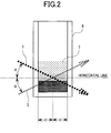
- Fig. 2 shows a partially enlarged view of Fig. 1, showing the portions of the container 6 and the sample solution 7 in enlargement and also showing the angle ⁇ of the transmitted light beams 1 and 2 with the wavelengths ⁇ 1 and ⁇ 2 with respect to the horizontal axis, in an exaggerated manner.
- the light beam 1 with the wavelength ⁇ 1 emitted by the semiconductor light source 2 is incident on the sample solution from upper left to lower right. Namely, it propagates from a portion of the sample solution with a smaller concentration and is then transmitted in the direction of portions with higher concentrations, forming only a slight angle ⁇ with respect to the horizontal axis.
- the light beam 3 with the wavelength ⁇ 2 emitted by the semiconductor light source 4 is incident on the sample solution from lower left to upper right, namely, from a portion of the sample solution with higher concentrations, the light beam then being transmitted in the direction of lower concentrations, also with a slight angle ⁇ with respect to the horizontal axis.
- the concentrations of the sample solution 7 are horizontally symmetric (symmetric with respect to the vertical axis). Therefore, the light beam 1 with the wavelength ⁇ 1 and the light beam 3 with the wavelength ⁇ 2 pass through portions with the same concentrations in different directions.
- the angle ⁇ is formed by the light beams 1 and 2 with the wavelengths ⁇ 1 and ⁇ 2 above and below the horizontal axis.
- the beams 1 and 3 with the wavelengths ⁇ 1 and ⁇ 2 each form an angle in opposite sides of the sheet of the drawing with respect to the horizontal axis, namely, when the light beams 1 and 3 with the wavelengths ⁇ 1 and ⁇ 2 are substantially in the same horizontal plane, the light beams 1 and 3 pass through portions with the same concentration and they are not influenced by the concentrations even though they have different optical transmission paths. This is true whether or not they intersect with one another at the substantially 1/2 length position in the sample solution 7 in the direction of transmission.
- a container is horizontally moved while being irradiated with light.
- the semiconductor light sources 2 and 4 are housed in the package 5 such that the light beams 1 and 3 with the wavelengths ⁇ 1 and ⁇ 2, after passing through the sample solution 5 under the aforementioned conditions, are shone on the detector 9 without loss.
- the simple structure which does not employ expensive optical equipment consisting of prisms and half mirrors for causing the optical axes of light beams of two different wavelengths to be aligned, can produce the same effects as obtained in the case of using such expensive optical equipment.
- an optical system capable of detecting minute amounts of sample in a solution with high sensitivity and accuracy can be provided.
- the analyzer includes an electric signal processing system installed around the above-described optical components, as shown in a block diagram.
- a signal with the frequency f1 oscillated by an oscillator circuit 10 is amplified by a drive circuit 11 and then fed to the semiconductor light source 2, so that the semiconductor light source 2 can emit the light beam 1 with the wavelength ⁇ 1 and the modulation frequency of f1.
- a signal with the frequency f2 is oscillated by an oscillator circuit 12, amplified by a drive circuit 13, and then fed to the semiconductor light source 4, so that the semiconductor light source 4 can emit the light beam 3 with the wavelength ⁇ 2 and the modulation frequency f2.
- the oscillator circuit 10 may incorporate the function of the drive circuit 11 and the oscillator circuit 12 that of the drive circuit 13.
- the light beam 1 with the wavelength ⁇ 1 and modulation frequency f1 emitted by the semiconductor light source 2 and the light beam 3 with the wavelength ⁇ 2 and modulation frequency of f2 emitted by the semiconductor light source 4 pass through the sample solution 7 along the aforementioned paths and are eventually detected by the detector 9.
- the detector 9 converts the light beams 1 and 3 with the wavelengths ⁇ 1 and ⁇ 2 and modulation frequencies of f1 and f2, which are attenuated and composed by the sample solution 7 or the like, into an electric signal.
- the electric signal outputted from the detector 9, which consists of the frequencies f1 and f2, is amplified by an amplifier 14 and then separated into the individual frequency components f1 and f2 by a frequency separation circuit 15 comprised of an FFT or BPF, for example.
- the signals with the frequencies f1 and f2 separated by the frequency separation circuit 15, which are analog signals, are converted into digital signals, the former by an A/D converter 16 and the latter by an A/D converter 17.
- the digital signals are then sent to a data processing unit 18.
- the signal with the frequency f1 contains the information regarding the wavelength ⁇ 1, enabling comparison as to how much the light beam 1 with the wavelength ⁇ 1 has been attenuated by the sample solution 7 or the like.
- the signal with the frequency f2 separated by the frequency separation circuit 15 contains information about the wavelength ⁇ 2, enabling comparison as to how much the light beam 3 with the wavelength ⁇ 2 has been attenuated by the sample solution 7 or the like.
- the reference for the comparison is the measurement data obtained in the case where the container 6 does not contain the sample solution 7, or the measurement data obtained with a reference reagent, such as purified water.
- an analyzer can be constructed which is capable of acquiring required frequency components without a diffraction grating and determining the amounts of target components by calculating their absorbance.
- portions that could have an adverse effect on detection are preferably avoided, such as the surface of the sample where there is surface tension, or the bottom of the container, for example.
- sample examples include those containing components with different specific gravities, such as blood serum and blood plasma.
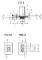
- Fig. 3 shows two different semiconductor light sources, a sample solution in a container, and a detector, together with the indications of the thickness of optical axes or the like.
- Fig. 4 shows light beams 1 and 3 with the wavelengths ⁇ 1 and ⁇ 2 incident on the detector.
- the electric signal processing system shown in Fig. 1 will be omitted in the descriptions referring to Fig. 3 and subsequent figures.
- the semiconductor light sources 2 and 4 are accommodated in the package 5 and adjusted such that the light beams 1 and 3 with the wavelengths ⁇ 1 and ⁇ 2 emitted thereby can intersect with one another at the position in the sample solution 7 that is substantially 1/2 of the length of the light beams in their directions of transmission, before they are incident on the detector 9.
- the influence of concentration arising from the difference in optical paths along which the two beams of light travel can be reduced, such that the measurement accuracy is less affected, as mentioned above.
- This effect can be expressed by a mathematical expression as follows.
- the distance P between the semiconductor light sources 2 and 4 must be such that the relationship P ⁇ a/b (W - D) is satisfied, where a is the distance between the semiconductor light sources 2 and 4 and X, which is the substantially 1/2 position of the length of the light beams in the sample in the direction of transmission in the horizontal direction with reference to Figs.
- b is the distance between X and the detector 9; W is the width of the photo-receiving plane of the detector 9; D is the maximum diameter on the photo-receiving plane of the light beams 1 and 3 with the wavelengths ⁇ 1 and ⁇ 2 emitted by the semiconductor light sources 2 and 4, respectively; and Q is the distance between the centers of the light beams 1 and 3 with the wavelengths ⁇ 1 and ⁇ 2 as projected on the detector 9.
- the light beams 1 and 3 with the wavelengths ⁇ 1 and ⁇ 2 are incident on the photo-receiving plane of the detector 9 not perpendicularly but with a slight angle with respect to the normal to the plane.
- the light beams 1 and 3 with their wavelengths ⁇ 1 or ⁇ 2 produce a projection 19 and a projection 20, respectively, as shown in Fig. 4, which are slightly larger than the diameter of the cross-section of each of the light beams 1 and 3 taken in the direction perpendicular to their respective optical axes.
- the projections 19 and 20 would be elliptical, with the diameter D indicating the maximum length of the projection.
- the effect of the projections 19 and 20 of the light beams 1 and 3, respectively, are the same whether they are spaced apart from one another, as shown in Fig. 4(b), or overlapped, as shown in Fig. 4(a), on the photo-receiving plane of the detector 9.
- Fig. 5 shows the above-described concept implemented in Embodiment 1.
- Embodiments 1 and 2 related to examples in which the first and second light beams are hardly diffused because of the use of semiconductor lasers, for example, in the light sources.
- the light sources are light-emitting diodes, for example, the light emitted by the device would be diffused, such that the light beams would have to be narrowed in the event that the volume of the sample solution is very small.
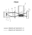
- Fig. 6 shows an embodiment involving the use of, e.g., light-emitting diodes in the light sources.
- the semiconductor light sources 2 and 4 emitting light beams 1 and 3 with the wavelengths ⁇ 1 and ⁇ 2, respectively, are housed in a package 5 made of a transparent resin, for example.
- a tip portion 21 of the package 5 via which the light beams emerge is formed in the shape of a convex lens so that the outgoing light beams from the internal light sources can be formed into substantially parallel light beams.
- the light beams 1 and 3 with the wavelengths ⁇ 1 and ⁇ 2 emitted from the internal semiconductor light sources 2 and 4 in the package 5, respectively are formed into substantially parallel beams with a large distance therebetween when they emerge from the package 5.
- the thus widely formed parallel beams of light beams 1 and 3 with the wavelengths ⁇ 1 and ⁇ 2 are then focused by a lens 22 at the substantially 1/2 position in the sample solution 7 of the length of the beams in the direction of transmission.
- the beams then pass through the sample solution while again being spread, and they are eventually shone on the detector 9.
- the beams 1 and 3 with the wavelengths ⁇ 1 and ⁇ 2 are not influenced by the concentrations of the sample due to the difference in their optical paths, as in Embodiments 1 and 2.
- the amounts of components in the sample are determined by detecting an optical signal from a detector on which two beams of light with different wavelengths that have passed through the sample solution in a container are incident.
- the analyzer is adapted such that, after the two beams of light with different wavelengths pass through a sample solution in a container, they are reflected by a wall surface of the container on the opposite side to the incident plane. The beams again pass through the sample solution and then detected by a detector housed in a package together with the semiconductor light source with the two different wavelengths.
- Fig. 7 shows the present embodiment in which the detector is housed in the same package containing the semiconductor light sources with the two different wavelengths.
- the embodiment involves an example where the light beams emitted by the light sources, such as light-emitting diodes, are diffused, as in Embodiment 3.
- semiconductor lasers the light emitted from which is not diffused, may be similarly employed as the light sources.
- the semiconductor light source 2 emitting light beam 1 with the wavelength ⁇ 1 and the semiconductor light source 4 emitting light beam 3 with the wavelength ⁇ 2 are both housed in a package 5' made of a transparent resin, for example.
- a detector 9' which corresponds to the detector 9 that has been disposed on the opposite side to the light sources with respect to the sample solution 7 in Embodiments 1 to 3, is housed in the same package 5' as for the semiconductor light sources 2 and 4.
- a container 6' in which the sample solution 7 is contained is constructed with a wall surface 24.
- the wall surface 24 (the internal or external surface of the container 6', or the walls of the container 6' by themselves) is disposed opposite to and substantially parallel with the wall surface on which the light beams 1 and 3 with the wavelengths ⁇ 1 and ⁇ 2 are incident, and is adapted to reflect the light beams 1 and 3 with the wavelengths ⁇ 1 and ⁇ 2.
- the light beams 1 and 3 with the wavelengths ⁇ 1 and ⁇ 2 emitted from the semiconductor light sources 2 and 4, respectively, are formed into substantially parallel beams at a tip portion 21 of the package 5' via which the beams emerge.
- the substantially parallel beams then pass through a lens 22' and are then shone on the container 6'.
- the beams 1 and 3 then enter the container 6' via an incident plane 23 thereof, pass through the sample solution 7, and then focused at and reflected by the reflecting plane 24 opposite to and substantially parallel with the incident plane of the container 6', producing reflected light beams 25.
- the reflected light beams 25 pass through the sample solution 7 again and exit the container 6' via the incident plane 23 thereof.
- the light beams 1 and 3 with the wavelengths ⁇ 1 and ⁇ 2 that have emerged out of the container 6' are formed into substantially parallel beams by the lens 22', and they are then focused onto the detector 9' after being formed by the tip portion 21 of the package 5' in the opposite manner to when they had emerged therefrom.
- the detector 9' is disposed between the semiconductor light sources 2 and 4, whose positions are adjusted such that the light beams 1 and 3 with the wavelengths ⁇ 1 and ⁇ 2 can be detected by the detector 9' efficiently.
- the detector 9' is closely surrounded by a light-blocking wall 26 so as to prevent the light from the semiconductor light sources 2 and 4 from entering the detector 9', either directly from the light sources or in the form of stray light produced by the light from the semiconductor light source 2 or 4 having been reflected by the external wall of the package 5'.
- the light-blocking wall 26 is electrically conducting, so that it can prevent the electric signals from the oscillator circuit 10 and oscillator circuit 12 of Embodiment 1 shown in Fig. 1 from entering into semiconductor light sources 2 and 4 as noise.
- the reflected beams then pass through the sample solution 7 again and emerge out of the container 6' via the incident plane 23.
- the optical paths are twice as long, so that an increase in sensitivity can be achieved.
- the light beams intersect with one another at the substantially 1/2 position of the length of the optical paths that are twice as long before they are reflected, the influence of concentration due to the difference in optical paths of the two beams of light can be eliminated, as in Embodiments 1 to 3.
- the light sources and the detector are housed in the same package, the size of the apparatus can be reduced.
- the position at which the beams 1 and 3 with the wavelengths ⁇ 1 and ⁇ 2 intersect with one another is set to be the substantially 1/2 position of the length of the optical path, or the substantially 1/2 position of the length of the optical path that has been made twice as long by reflection.
- the intersecting position is different from those of the foregoing embodiments.
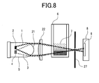
- Fig. 8 schematically shows the present embodiment in which the aforementioned intersecting position is set to be located between the container 6 and detector 9.
- the position of the semiconductor light sources 2 and 4 are adjusted such that the position at which the beams 1 and 3 with the wavelengths ⁇ 1 and ⁇ 2, respectively, is located between the container 6 and the detector 9.
- an aperture 27 can be disposed at the intersecting position. The aperture 27 can be used to eliminate unwanted stray light other than the beams 1 ( ⁇ 1) and 3 ( ⁇ 2) that could be incident on the detector 9, thereby improving detection accuracy.
- the present embodiment cannot provide the advantage relating to the absence of influence of concentration due to the difference in the optical paths of the two beams, as described with reference to Embodiments 1 to 4. Thus, it is important to clarify the purpose before adopting the concept of the present embodiment.
- the detector 9 is housed in a conducting member 28 such that wiring leads 29 are not in contact with the conducting member.
- the incident plane of the detector 9 is covered with a transparent member 31 of thin glass or the like.
- the transparent member 31 is coated with a transparent electrically conducting film 30, such as an ITO, at least on that side thereof which is in contact with the conducting member 28.
- the conducting member 28 and the transparent film 30 are thus grounded so as to prevent noise.
- One of the two wiring leads 29 is grounded while the other is insulated from the surrounding members. Namely, the detection system is covered with planes that are almost all grounded except for one of the wiring leads, so that noise can be prevented.
- package 5' containing the detector 9' and the semiconductor light sources 2 and 4 is contained in a conducting member 28' such that wiring leads 29' are not in contact with the conducting member 28', as shown in Fig. 9(b).
- the incident/outgoing plane of the package 5' is covered with a lens 22' coated with a transparent electrically conducting film 30', such as an ITO, at least on the side thereof that is in contact with the conducting member 28'.
- the conducting member 28', the transparent electrically conducting film 30', and the aforementioned light-blocking wall 26 are grounded so as to prevent noise.
- four wiring leads are shown as an example, of which two are used for detection. One of the detection leads is grounded while the other is insulated from the other surrounding members.
- the two light sources and most of the other portions except for one of the wiring leads are covered with planes that are grounded, so that noise can be prevented.
- Similar effects may be obtained by covering the exterior of the detector 9 or the package 5' with a transparent electrically conducting film, such as an ITO, to the extent that the film is not in contact with the wiring leads 29 and 29', and connecting the film to ground.
- a transparent electrically conducting film such as an ITO
- the peak wavelength, or the wavelength for the greatest amount of a component, of the light emitted by the semiconductor light sources 2 and 4 is a particular combination of two different wavelengths selected from the group of 13 wavelengths consisting of substantially 340, 405, 415, 450, 480, 505, 546, 570, 600, 660, 700, 750, and 800 nm.
- the entire examination items that are currently measurable using automatic biochemical analyzers can be covered without changing the protocol of the reagents used.
- those including ultraviolet ray of the wavelength of 340 nm for one of the wavelengths are most likely. This is due to the fact that there are many examination items or examination reagents for which combinations of the wavelength of 340 nm and another wavelength are suitable. It is very important to select ultraviolet ray for one of the wavelengths of a combination.
- the invention can be employed for analyzing components, such as biological components in particular.
Abstract
Description
Patent Publication 1: JP Patent Publication (Kokai) No. 8-122247 A (1996)
Patent Publication 2: JP Patent Publication (Kokai) No. 2002-340676 A
Patent Publication 3: JP Patent Publication (Kokai) No. 2001-159601 A
Claims (17)
- A sample analyzer comprising:a sample container for carrying a sample;a first light source for emitting a light beam of a first wavelength with which said sample is irradiated;a second light source for emitting a light beam of a second wavelength with which said sample is irradiated; anda detector for detecting a first beam of light which is said light beam of said first wavelength that has passed through said sample, and a second beam of light which is said light beam of said second wavelength that has passed though said sample, whereinsaid light beam of said first wavelength intersects with said light beam of said second wavelength at a substantially 1/2 position in said sample of the length of said beams in the direction of transmission thereof.
- The sample analyzer according to claim 1, wherein said first light source and said second light source are housed in a single package.
- The sample analyzer according to claim 1, wherein said first light source and said second light source comprise semiconductor lasers.
- The sample analyzer according to claim 1, wherein
said first light source and said second light source comprise light-emitting diodes, said first light source and said second light source being housed in a package with a light-emerging portion via which said light beams from said first and said second light sources emerge, said light-emerging portion being formed in the shape of a convex lens such that the light beams emitted by said first light source and said second light source are formed into substantially parallel light beams, said sample analyzer further comprising:a focusing lens disposed between said package, which is made of a transparent resin or the like, and said sample container. - The sample analyzer according to claim 1, further comprising:a first oscillator circuit for modulating said light beam of said first wavelength into a first frequency;a second oscillator circuit for modulating said light beam of said second wavelength into a second frequency; anda frequency separation circuit for separating a signal detected by said detector into components of said first frequency and said second frequency.
- The sample analyzer according to claim 1, wherein
said detector comprises a photodiode with a photo-receiving plane thereof being covered with a transparent electrically conducting film that is grounded, said photodiode having two electrodes of which one is grounded, said photodiode being almost entirely covered with planes connected to ground except for the other of said two electrodes thereof. - The sample analyzer according to claim 1, wherein the wavelength of one of the light beams emitted by said first light source and said second light source is that of an ultraviolet ray.
- The sample analyzer according to claim 1, wherein the peak wavelengths of the light beams emitted by said first light source and said second light source, or the wavelengths of said light beams at which the maximum amounts of components are obtained, are two different wavelengths selected from the group consisting of substantially 340, 405, 415, 450, 480, 505, 546, 570, 600, 660, 700, 750, and 800 (nm).
- A sample analyzer comprising:a sample container for carrying a sample;a first light source for emitting a light beam of a first wavelength with which said sample is irradiated;a second light source for emitting a light beam of a second wavelength with which said sample is irradiated; anda detector for detecting a first light beam which is said light beam of said first wavelength that has passed through said sample, and a second light beam which is said light beam of said second wavelength that has passed through said sample, wherein
the relationship P < a/b (W - D) is satisfied, where a is the distance between said first and second light sources and X, which is a position in the horizontal direction at which said light beams of said first and second wavelengths intersect with one another; b is the distance between X and said detector; P is the distance between said first and said second light sources; W is the width of a photo-receiving plane of said detector; D is the maximum diameter on said photo-receiving plane of said first and said second light beams emitted by said first and said second light sources, respectively; and Q is the distance between the centers of said first and said second light beams on said photo-receiving plane, wherein X is located at a substantially 1/2 position in said sample of the length of said beams in the direction of transmission thereof in the horizontal direction. - The sample analyzer according to claim 9, wherein said first and said second light sources are housed in a single package.
- The sample analyzer according to claim 9, wherein said first light source and said second light source comprise diodes, said first light source and said second light source being housed in a package with a light-emerging portion via which the light beams from said first and said second light sources emerge, said light-emerging portion being formed in the shape of a convex lens such that said light beams emitted by said first light source and said second light source can be formed into substantially parallel beams of light, said sample analyzer further comprising:a focusing lens disposed between said package and said sample container.
- A sample analyzer comprising:a sample container for carrying a sample;a first light source for emitting a light beam of a first wavelength with which said sample is irradiated;a second light source for emitting a light beam of a second wavelength with which said sample is irradiated; anda detector for detecting a first light beam which is said light beam of said first wavelength that has passed through said sample, and a second light beam which is said light beam of said second wavelength that has passed through said sample, whereinsaid sample container comprises a transparent portion and a reflecting portion that reflects light, wherein said sample is irradiated with said light beam of said first wavelength and said light beam of said second wavelength via said transparent portion of said sample container, said light beams passing through said sample and then being reflected by said reflecting portion, said light beams again passing through said sample and emerging via said transparent portion to be detected by said detector, and whereinsaid first light source, said second light source, and said detector are disposed such that said light beam of said first wavelength and said light beam of said second wavelength can be captured by said detector after having once intersecting with one another substantially at said reflecting portion and reflected thereby.
- The sample analyzer according to claim 12, wherein said first light source, said second light source, and said detector are housed in a single package.
- The sample analyzer according to claim 12, wherein said detector is disposed between said first light source and said second light source.
- The sample analyzer according to claim 12, wherein a light-blocking wall is provided around said detector.
- The sample analyzer according to claim 12, wherein said detector comprises a photodiode of which at least a photo-receiving plane is covered with a transparent, electrically conducting film that is grounded, said photodiode having two electrodes of which one is grounded, and wherein almost all of the parts are entirely covered with planes that are connected to ground except for the other of said two electrodes and the electrodes of said first light source and said second light source.
- A sample analyzer comprising:a sample container for carrying a sample;a first light source for emitting a light beam of a first wavelength with which said sample is irradiated;a second light source for emitting a light beam of a second wavelength with which said sample is irradiated; anda detector for detecting a first light beam which is said light beam of said first wavelength that has passed through said sample, and a second light beam which is said light beam of said second wavelength that has passed through said sample, whereinsaid light beam of said first wavelength and said light beam of said second wavelength intersect with one another between said container and said detector, said sample analyzer further comprising:an aperture disposed at the point of intersection.
Applications Claiming Priority (2)
| Application Number | Priority Date | Filing Date | Title |
|---|---|---|---|
| JP2004151177A JP4491277B2 (en) | 2004-05-21 | 2004-05-21 | Sample analyzer |
| JP2004151177 | 2004-05-21 |
Publications (2)
| Publication Number | Publication Date |
|---|---|
| EP1598658A2 true EP1598658A2 (en) | 2005-11-23 |
| EP1598658A3 EP1598658A3 (en) | 2007-03-28 |
Family
ID=34936611
Family Applications (1)
| Application Number | Title | Priority Date | Filing Date |
|---|---|---|---|
| EP20050010688 Withdrawn EP1598658A3 (en) | 2004-05-21 | 2005-05-17 | Sample analyzer |
Country Status (3)
| Country | Link |
|---|---|
| US (1) | US7342662B2 (en) |
| EP (1) | EP1598658A3 (en) |
| JP (1) | JP4491277B2 (en) |
Cited By (3)
| Publication number | Priority date | Publication date | Assignee | Title |
|---|---|---|---|---|
| CN102621087A (en) * | 2012-03-23 | 2012-08-01 | 上海欣茂仪器有限公司 | Large plain film spectrum tester |
| CN105466875A (en) * | 2015-11-23 | 2016-04-06 | 中国科学院青海盐湖研究所 | Method for measuring dodecylmorpholine |
| CN109085143A (en) * | 2016-08-25 | 2018-12-25 | 任文利 | A kind of haemoconcentration detection device |
Families Citing this family (11)
| Publication number | Priority date | Publication date | Assignee | Title |
|---|---|---|---|---|
| CN102519887B (en) | 2005-03-29 | 2015-09-09 | 希森美康株式会社 | Sample analyzing method and sample analyzer |
| CN103941027B (en) | 2005-03-29 | 2016-09-07 | 希森美康株式会社 | Sample analyzing method and specimen analyzing device |
| JP4875391B2 (en) * | 2006-03-30 | 2012-02-15 | シスメックス株式会社 | Sample analyzer |
| JP2008020380A (en) * | 2006-07-14 | 2008-01-31 | Aloka Co Ltd | Absorbance measuring instrument |
| JP2008020381A (en) * | 2006-07-14 | 2008-01-31 | Aloka Co Ltd | Absorbance measuring instrument |
| JP2008026036A (en) * | 2006-07-18 | 2008-02-07 | Aloka Co Ltd | Inclusion measuring device |
| KR101309129B1 (en) * | 2012-03-15 | 2013-09-16 | 주식회사 메카시스 | Sample handler for analyzing a small quantity of sample, analyzing apparatus using the sample handler, and analyzing method |
| CN103645119B (en) * | 2013-12-17 | 2015-12-09 | 哈尔滨工程大学 | A kind of measurement mechanism of the area array CCD liquid density measurement based on pointolite |
| JP6657016B2 (en) * | 2016-05-27 | 2020-03-04 | 株式会社日立ハイテクノロジーズ | Automatic analyzer |
| CN109060697A (en) * | 2018-10-24 | 2018-12-21 | 深圳市长隆科技有限公司 | Automatically select the water quality parameter analyzer of Detection wavelength |
| CN112683850A (en) * | 2020-11-30 | 2021-04-20 | 深圳市科曼医疗设备有限公司 | Detection method, system and storage medium of C-reactive protein |
Citations (1)
| Publication number | Priority date | Publication date | Assignee | Title |
|---|---|---|---|---|
| US20010026011A1 (en) * | 1999-03-15 | 2001-10-04 | Roberts John K. | Radiation emitter devices and method of making the same |
Family Cites Families (16)
| Publication number | Priority date | Publication date | Assignee | Title |
|---|---|---|---|---|
| GB918616A (en) * | 1960-06-15 | 1963-02-13 | Sir Howard Grubb Parsons | Improvements in and relating to photographic plate or film measuring devices |
| JPS6011143A (en) * | 1983-07-01 | 1985-01-21 | Toshiba Corp | Measuring apparatus of absorbance |
| US4573796A (en) * | 1984-01-06 | 1986-03-04 | The United States Of America As Represented By The United States Department Of Energy | Apparatus for eliminating background interference in fluorescence measurements |
| US4893929A (en) * | 1987-03-13 | 1990-01-16 | Canon Kabushiki Kaisha | Particle analyzing apparatus |
| JPH0623691B2 (en) * | 1987-05-25 | 1994-03-30 | 株式会社日立製作所 | Atomic absorption spectrophotometer |
| JPS6421070A (en) * | 1987-07-17 | 1989-01-24 | Matsushita Electric Ind Co Ltd | Production of thin metal film and device therefor |
| US4999513A (en) * | 1988-09-09 | 1991-03-12 | Canon Kabushiki Kaisha | Particle measuring apparatus |
| EP0448931B1 (en) * | 1990-01-26 | 1996-04-03 | Canon Kabushiki Kaisha | Method for measuring a specimen by the use of fluorescence light |
| JP3223461B2 (en) * | 1993-01-14 | 2001-10-29 | 能美防災株式会社 | Pyroelectric element |
| JPH08122247A (en) * | 1994-10-24 | 1996-05-17 | Hitachi Ltd | Analyzer |
| JPH09105717A (en) * | 1995-10-11 | 1997-04-22 | Yokogawa Electric Corp | Spectroscopic analyzer |
| JP2001013065A (en) * | 1999-06-28 | 2001-01-19 | Kubota Corp | Egg inspection apparatus |
| JP2001159601A (en) | 1999-11-30 | 2001-06-12 | Mitsubishi Chemicals Corp | Optical measuring apparatus |
| JP2002340676A (en) | 2001-05-16 | 2002-11-27 | Canare Electric Co Ltd | Multi-channel modulation spectrometric method and multi-channel modulation spectrometric device |
| JP3821727B2 (en) * | 2002-02-26 | 2006-09-13 | 株式会社クボタ | Spectroscopic analyzer |
| FR2845777B1 (en) | 2002-10-11 | 2005-01-07 | Commissariat Energie Atomique | OPTICAL DEVICE PRODUCING TWO BEAMS CAPABLE OF REACHING A COMMON DETECTOR |
-
2004
- 2004-05-21 JP JP2004151177A patent/JP4491277B2/en not_active Expired - Fee Related
-
2005
- 2005-05-17 EP EP20050010688 patent/EP1598658A3/en not_active Withdrawn
- 2005-05-19 US US11/132,291 patent/US7342662B2/en not_active Expired - Fee Related
Patent Citations (1)
| Publication number | Priority date | Publication date | Assignee | Title |
|---|---|---|---|---|
| US20010026011A1 (en) * | 1999-03-15 | 2001-10-04 | Roberts John K. | Radiation emitter devices and method of making the same |
Cited By (4)
| Publication number | Priority date | Publication date | Assignee | Title |
|---|---|---|---|---|
| CN102621087A (en) * | 2012-03-23 | 2012-08-01 | 上海欣茂仪器有限公司 | Large plain film spectrum tester |
| CN102621087B (en) * | 2012-03-23 | 2014-03-26 | 上海欣茂仪器有限公司 | Large plain film spectrum tester |
| CN105466875A (en) * | 2015-11-23 | 2016-04-06 | 中国科学院青海盐湖研究所 | Method for measuring dodecylmorpholine |
| CN109085143A (en) * | 2016-08-25 | 2018-12-25 | 任文利 | A kind of haemoconcentration detection device |
Also Published As
| Publication number | Publication date |
|---|---|
| US20050259261A1 (en) | 2005-11-24 |
| JP4491277B2 (en) | 2010-06-30 |
| US7342662B2 (en) | 2008-03-11 |
| EP1598658A3 (en) | 2007-03-28 |
| JP2005331422A (en) | 2005-12-02 |
Similar Documents
| Publication | Publication Date | Title |
|---|---|---|
| US7342662B2 (en) | Sample analyzer | |
| KR960038386A (en) | Optical detection device for chemical analysis measurement | |
| JP2001141654A (en) | Spectral luminous intensity and specific turbidity detecting unit | |
| EP2726852B1 (en) | Multiple examinations of a sample | |
| JP5824325B2 (en) | System for scattering and absorption analysis | |
| JP2019518941A (en) | Transient hemolysis detection | |
| JP6733664B2 (en) | Detecting chip manufacturing method and detecting chip | |
| US7173705B2 (en) | Measuring device for immunochromatography test piece | |
| JP7336695B2 (en) | optical device | |
| US7173704B2 (en) | Measuring device for immunochromatography test piece and light source device | |
| JP2008026036A (en) | Inclusion measuring device | |
| JP2010091441A (en) | Light quantity monitoring apparatus and light quantity monitoring method | |
| JP2000230901A (en) | Optical unit | |
| EP0903571A2 (en) | Apparatus and method for determining the concentration of specific substances | |
| JP4742166B2 (en) | Sample analyzer | |
| JP2010156557A (en) | Incident optical system and raman scattering measurement apparatus | |
| US6788415B2 (en) | Turntable measuring apparatus utilizing attenuated total reflection | |
| JP3903871B2 (en) | Surface plasmon element and inspection apparatus using the same | |
| JP2010091428A (en) | Scanning optical system | |
| CN220084709U (en) | Optical detection device and specific protein analyzer | |
| JP2002168779A (en) | Refractive index change measuring instrument | |
| JP2000171396A (en) | Concentration detecting device for oil deteriorating matter | |
| JP2005147891A (en) | Surface plasmon resonance sensor | |
| US20030105392A1 (en) | Apparatus for measuring concentration of a specific ingredient in-situ | |
| JP2002139422A (en) | Light absorption measuring instrument for light scattering medium |
Legal Events
| Date | Code | Title | Description |
|---|---|---|---|
| PUAI | Public reference made under article 153(3) epc to a published international application that has entered the european phase |
Free format text: ORIGINAL CODE: 0009012 |
|
| AK | Designated contracting states |
Kind code of ref document: A2 Designated state(s): AT BE BG CH CY CZ DE DK EE ES FI FR GB GR HU IE IS IT LI LT LU MC NL PL PT RO SE SI SK TR |
|
| AX | Request for extension of the european patent |
Extension state: AL BA HR LV MK YU |
|
| PUAL | Search report despatched |
Free format text: ORIGINAL CODE: 0009013 |
|
| AK | Designated contracting states |
Kind code of ref document: A3 Designated state(s): AT BE BG CH CY CZ DE DK EE ES FI FR GB GR HU IE IS IT LI LT LU MC NL PL PT RO SE SI SK TR |
|
| AX | Request for extension of the european patent |
Extension state: AL BA HR LV MK YU |
|
| 17P | Request for examination filed |
Effective date: 20070606 |
|
| AKX | Designation fees paid |
Designated state(s): DE FR |
|
| 17Q | First examination report despatched |
Effective date: 20090313 |
|
| STAA | Information on the status of an ep patent application or granted ep patent |
Free format text: STATUS: THE APPLICATION IS DEEMED TO BE WITHDRAWN |
|
| 18D | Application deemed to be withdrawn |
Effective date: 20151201 |