EP1594177B1 - Organic electro-luminescence display device and fabricating method thereof - Google Patents
Organic electro-luminescence display device and fabricating method thereof Download PDFInfo
- Publication number
- EP1594177B1 EP1594177B1 EP05009663A EP05009663A EP1594177B1 EP 1594177 B1 EP1594177 B1 EP 1594177B1 EP 05009663 A EP05009663 A EP 05009663A EP 05009663 A EP05009663 A EP 05009663A EP 1594177 B1 EP1594177 B1 EP 1594177B1
- Authority
- EP
- European Patent Office
- Prior art keywords
- organic
- display device
- organic electro
- luminescence
- barrier rib
- Prior art date
- Legal status (The legal status is an assumption and is not a legal conclusion. Google has not performed a legal analysis and makes no representation as to the accuracy of the status listed.)
- Active
Links
- 238000005401 electroluminescence Methods 0.000 title claims abstract description 110
- 238000000034 method Methods 0.000 title abstract description 18
- 230000004888 barrier function Effects 0.000 claims abstract description 69
- 239000000758 substrate Substances 0.000 claims abstract description 34
- 239000000565 sealant Substances 0.000 claims description 37
- 230000006866 deterioration Effects 0.000 abstract description 9
- 238000005530 etching Methods 0.000 description 8
- 238000000206 photolithography Methods 0.000 description 8
- 238000000151 deposition Methods 0.000 description 7
- 238000000059 patterning Methods 0.000 description 6
- 108091006149 Electron carriers Proteins 0.000 description 5
- 238000004519 manufacturing process Methods 0.000 description 5
- QVGXLLKOCUKJST-UHFFFAOYSA-N atomic oxygen Chemical compound [O] QVGXLLKOCUKJST-UHFFFAOYSA-N 0.000 description 4
- 239000004020 conductor Substances 0.000 description 4
- 239000007769 metal material Substances 0.000 description 4
- 239000001301 oxygen Substances 0.000 description 4
- 229910052760 oxygen Inorganic materials 0.000 description 4
- XOLBLPGZBRYERU-UHFFFAOYSA-N tin dioxide Chemical compound O=[Sn]=O XOLBLPGZBRYERU-UHFFFAOYSA-N 0.000 description 4
- 238000005538 encapsulation Methods 0.000 description 3
- 150000002894 organic compounds Chemical class 0.000 description 3
- 230000003044 adaptive effect Effects 0.000 description 2
- 239000011248 coating agent Substances 0.000 description 2
- 238000000576 coating method Methods 0.000 description 2
- 239000011521 glass Substances 0.000 description 2
- AMGQUBHHOARCQH-UHFFFAOYSA-N indium;oxotin Chemical compound [In].[Sn]=O AMGQUBHHOARCQH-UHFFFAOYSA-N 0.000 description 2
- 238000002347 injection Methods 0.000 description 2
- 239000007924 injection Substances 0.000 description 2
- 239000011810 insulating material Substances 0.000 description 2
- 239000000463 material Substances 0.000 description 2
- 239000002184 metal Substances 0.000 description 2
- 239000011368 organic material Substances 0.000 description 2
- HUAUNKAZQWMVFY-UHFFFAOYSA-M sodium;oxocalcium;hydroxide Chemical compound [OH-].[Na+].[Ca]=O HUAUNKAZQWMVFY-UHFFFAOYSA-M 0.000 description 2
- 238000004528 spin coating Methods 0.000 description 2
- 239000000969 carrier Substances 0.000 description 1
- 238000010586 diagram Methods 0.000 description 1
- 238000007598 dipping method Methods 0.000 description 1
- 239000003822 epoxy resin Substances 0.000 description 1
- BHEPBYXIRTUNPN-UHFFFAOYSA-N hydridophosphorus(.) (triplet) Chemical compound [PH] BHEPBYXIRTUNPN-UHFFFAOYSA-N 0.000 description 1
- 239000012535 impurity Substances 0.000 description 1
- 239000004973 liquid crystal related substance Substances 0.000 description 1
- 238000012986 modification Methods 0.000 description 1
- 230000004048 modification Effects 0.000 description 1
- 238000004806 packaging method and process Methods 0.000 description 1
- 229920000647 polyepoxide Polymers 0.000 description 1
- 238000000926 separation method Methods 0.000 description 1
Images


Classifications
-
- H—ELECTRICITY
- H10—SEMICONDUCTOR DEVICES; ELECTRIC SOLID-STATE DEVICES NOT OTHERWISE PROVIDED FOR
- H10K—ORGANIC ELECTRIC SOLID-STATE DEVICES
- H10K50/00—Organic light-emitting devices
- H10K50/80—Constructional details
- H10K50/84—Passivation; Containers; Encapsulations
- H10K50/842—Containers
- H10K50/8426—Peripheral sealing arrangements, e.g. adhesives, sealants
-
- H—ELECTRICITY
- H10—SEMICONDUCTOR DEVICES; ELECTRIC SOLID-STATE DEVICES NOT OTHERWISE PROVIDED FOR
- H10K—ORGANIC ELECTRIC SOLID-STATE DEVICES
- H10K59/00—Integrated devices, or assemblies of multiple devices, comprising at least one organic light-emitting element covered by group H10K50/00
- H10K59/10—OLED displays
- H10K59/17—Passive-matrix OLED displays
- H10K59/173—Passive-matrix OLED displays comprising banks or shadow masks
-
- H—ELECTRICITY
- H10—SEMICONDUCTOR DEVICES; ELECTRIC SOLID-STATE DEVICES NOT OTHERWISE PROVIDED FOR
- H10K—ORGANIC ELECTRIC SOLID-STATE DEVICES
- H10K59/00—Integrated devices, or assemblies of multiple devices, comprising at least one organic light-emitting element covered by group H10K50/00
- H10K59/80—Constructional details
- H10K59/87—Passivation; Containers; Encapsulations
- H10K59/871—Self-supporting sealing arrangements
- H10K59/8722—Peripheral sealing arrangements, e.g. adhesives, sealants
-
- H—ELECTRICITY
- H10—SEMICONDUCTOR DEVICES; ELECTRIC SOLID-STATE DEVICES NOT OTHERWISE PROVIDED FOR
- H10K—ORGANIC ELECTRIC SOLID-STATE DEVICES
- H10K59/00—Integrated devices, or assemblies of multiple devices, comprising at least one organic light-emitting element covered by group H10K50/00
- H10K59/80—Constructional details
- H10K59/88—Dummy elements, i.e. elements having non-functional features
-
- H—ELECTRICITY
- H10—SEMICONDUCTOR DEVICES; ELECTRIC SOLID-STATE DEVICES NOT OTHERWISE PROVIDED FOR
- H10K—ORGANIC ELECTRIC SOLID-STATE DEVICES
- H10K59/00—Integrated devices, or assemblies of multiple devices, comprising at least one organic light-emitting element covered by group H10K50/00
- H10K59/10—OLED displays
- H10K59/17—Passive-matrix OLED displays
- H10K59/179—Interconnections, e.g. wiring lines or terminals
Definitions
- This invention relates to an electro-luminescence display (ELD), and more particularly to an organic electro-luminescence display device and a fabricating method thereof that are adaptive for preventing a deterioration of light-emission efficiency and picture quality.
- ELD electro-luminescence display
- US 2003/080 678 Al shows an organic electro-luminescence display device comprising an organic electro-luminescence array having first electrodes and second electrodes provided on a substrate with an organic light-emitting layer therebetween, and a separator layer. A barrier portion is provided to enclose the organic electro-luminescent array completely. The device further comprises a cap joined with the substrate by a sealant to package the organic electro-luminescent array.
- various flat panel display devices reduced in weight and bulk that is capable of eliminating disadvantages of a cathode ray tube (CRT).
- Such flat panel display devices include a liquid crystal display (LCD), a field emission display (FED), a plasma display panel (PDP) and an electro-luminescence (EL) display, etc.
- LCD liquid crystal display
- FED field emission display
- PDP plasma display panel
- EL electro-luminescence
- the EL display device is a self-luminous device capable of light-emitting for himself.
- the EL display device excites a phosphorous material using carriers such as electrons and holes, thereby displaying a video image.
- the EL display device is largely classified into an inorganic EL display device and an organic EL display device depending upon the used material.
- the organic EL display device Since the organic EL display device is driven with a lower voltage (i.e., about 5 to 20V) than the inorganic EL display device requiring a high voltage of 100 to 200V, it permits a direct current low voltage driving. Also, since the organic EL display device has excellent characteristics such as a wide viewing angle, a fast response and a high contrast ratio, etc., it can be used for a pixel of a graphic display, or a pixel of a television image display or a surface light source. Further, the organic EL display device is a device suitable for a post generation flat panel display because it has a thin thickness, a light weight and an excellent color sense.
- Fig. 1 is a schematic view showing a structure of a general organic EL display device
- Fig. 2 is a detailed plan view of a portion (A area) in Fig. 1
- Fig. 3 is a section view of the portion of the organic El display device taken along the I -I ' and II-II' lines in Fig. 2 .
- the related art EL display device includes a display area P1 provided with an organic EL array having driving electrodes (e.g., an anode electrode and a cathode electrode), etc., and a non-display area P2 provided with a pad portion 25 for applying driving signals to the driving electrodes at the display area P1.
- driving electrodes e.g., an anode electrode and a cathode electrode
- non-display area P2 provided with a pad portion 25 for applying driving signals to the driving electrodes at the display area P1.
- the display area P1 is provided with an anode electrode 4 formed on a substrate 2, and a cathode electrode 12 formed in a direction crossing the anode electrode 4.
- a plurality of anode electrodes 4 are provided on the substrate 2 in such a manner to be spaced at a desired distance from each other.
- An insulting film 6 having an aperture for each EL cell area is formed on the substrate 2 provided with the anode electrode 4.
- a barrier rib 8 for making a separation of an organic light-emitting layer 10 and a cathode electrode 12 to be formed thereon is provided.
- the barrier rib 8 is formed in a direction crossing the anode electrode 4, and has an overhang structure in which the upper portion thereof has a larger width than the lower portion thereof.
- the organic light-emitting layer 10 made from an organic compound and the cathode electrode 12 are entirely deposited onto the insulating film 6 provided with the barrier rib 8.
- the organic light-emitting layer 10 is formed by depositing a hole carrier layer, a light-emitting layer and an electron carrier layer onto the insulating film 6.
- the non-display area P2 is provided with a first line 54 extended from the anode electrode 4 at the display area P1, data pads for supplying data voltages, via the first line 54, to the anode electrode 4, a second line 52 connected to the cathode electrode 12, and scan pads for supplying scan voltages via the second line 52.
- the second line 52 consists of a double layer having a transparent conductive layer 52a and an opaque conductive layer 52b.
- the data pad is connected to a tape carrier package (TCP) mounted with a first driving circuit for generating data voltages to thereby supply the data voltage to each anode voltage 4.
- TCP tape carrier package
- the scan pad is provided at each side of the data pad.
- the scan pad is connected to a TCP mounted with a second driving circuit for generating scan voltages to thereby supply the scan voltage to each cathode electrode 12.
- the organic EL array at the display area P1 has a characteristic liable to be deteriorated against moisture and oxygen.
- an encapsulating process is carried out to join the substrate 2 provided with the organic EL array of the anode electrode 2, etc. with a cap 28 by a sealant 25 such as an epoxy resin.
- a getter for absorbing the moisture and oxygen is filled into the rear center portion of the cap 28 to thereby protect an organic EL array from the oxygen and moisture.
- the sealant 25 may be frequently flown, via between the barrier rib 8 and the barrier rib 8, into the organic EL array of the display area P1 when the cap 28 is joined with the cap 2.
- the sealant 25 contains a large amount of moisture, oxygen and impurity to cause a damage to the organic light-emitting layer 10 of the organic EL array. Therefore, there is raised a problem in that a light-emission efficiency and a picture quality are deteriorated. Further prior art is known from US 2003/042852 A1 , US 5 742 129 A and US 2003/218 419 A1 .
- an object of the present invention to provide an organic electro-luminescence display device and a fabricating method thereof that are adaptive for preventing a deterioration of light-emission efficiency and picture quality.
- an organic electro-luminescence display device includes an organic electro-luminescence array having first and second electrodes provided on a substrate with having an organic light-emitting layer therebetween and a barrier rib parallel to any one of the first and second electrodes; and a dummy barrier rib connected to each of the barrier ribs and provided in such a manner to enclose the organic electro-luminescence array along with the barrier rib.
- the organic electro-luminescence display device further includes a cap joined with the substrate by a sealant to package the organic electro-luminescence array.
- the sealant is positioned at the outer areas of the barrier rib and the dummy barrier rib.
- the organic electro-luminescence display device further includes a signal supply pad for supplying a driving signal to the organic electro-luminescence array; and a signal line for electrically connecting any one of the first and second electrodes to the signal supply pad.
- the organic electro-luminescence display device further includes an insulating film for exposing a light-emitting area at the first electrode and for exposing the signal line, wherein any one of the first and second electrodes is connected, via said contact hole, to the signal line.
- An organic electro-luminescence display device in which a substrate provided with an organic electro-luminescence array is joined with a cap by a sealant in order to package the organic electro-luminescence array, according to another aspect of the present invention includes a first insulating pattern positioned between the organic electro-luminescence array and the sealant and provided in such a manner to have concave and convex portions.
- the organic electro-luminescence array includes first and second electrodes provided on a substrate with having an organic light-emitting layer therebetween; and a barrier rib being parallel to any one of the first and second electrodes.
- the organic electro-luminescence display device further includes a signal supply pad for supplying a driving signal to the organic electro-luminescence array; and a signal line for electrically connecting any one of the first and second electrodes to the signal supply pad.
- the organic electro-luminescence display device further includes a second insulating pattern having a contact hole for exposing a light-emitting area at the first electrode and for exposing the signal line, wherein any one of the first and second electrodes is connected, via said contact hole, to the signal line.
- a method of fabricating an organic electro-luminescence display device in which a substrate provided with an organic electro-luminescence array is joined with a cap by a sealant in order to package the organic electro-luminescence array, according to still another aspect of the present invention includes the step of forming a first insulating pattern positioned between the organic electro-luminescence array and the sealant and provided in such a manner to have concave and convex portions.
- Fig. 1 is a schematic view showing a structure of a related art organic electro-luminescence display device
- Fig. 2 is a detailed view of the A area of the organic electro-luminescence display device shown in Fig. 1 ;
- Fig. 3 is a section view of the portion of the organic El display device taken along the I -I ' and II -II' lines in Fig. 2 ;
- Fig. 4 is a diagram for explaining a light-emitting principle of the related art organic electro-luminescence display device
- Fig. 5 illustrates a portion of an organic electro-luminescence display device according to a first embodiment of the present invention
- Fig. 6 is a section view of the organic electro-luminescence display device taken along the III-III' and IV-IV' lines in Fig. 5 ;
- Fig. 7A to Fig. 7F are section views for sequentially explaining a method of fabricating the organic electro-luminescence display device shown in Fig. 6 ;
- Fig. 8 illustrates a portion of an organic electro-luminescence display device according to a second embodiment of the present invention
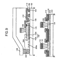
- Fig. 9 is a section view of the organic electro-luminescence display device taken along the III -III ' and IV-IV' lines in Fig. 8 ;
- Fig. 10A to Fig. 10F are section views for sequentially explaining a method of fabricating the organic electro-luminescence display device shown in Fig. 8 .
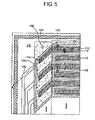
- Fig. 5 shows a portion of an organic electro-luminescence display device according to a first embodiment of the present invention
- Fig. 6 is a section view of the organic electro-luminescence display device taken along the III-III' and IV-IV' lines in Fig. 5 .
- the EL display device includes a display area P1 provided with an organic EL array having an anode electrode, etc., and a non-display area P2 provided with a pad portion for applying driving signals to the driving electrodes at the display area P1.
- the display area P1 is provided with an anode electrode 104 formed on a substrate 102, and a cathode electrode 112 formed in a direction crossing the anode electrode 104.
- a plurality of anode electrodes 104 are provided on the substrate 102 in such a manner to be spaced at a desired distance from each other.
- An insulting film 106 having an aperture for defining a light-emitting area for each EL cell area and a contact hole 175 for exposing a second line 152 is formed on the substrate 102 provided with the anode electrode 104.
- a barrier rib 108 having an overhang structure in which the upper portion thereof has a larger width than the lower portion thereof is provided on the insulating film 106.
- the barrier rib 108 plays a role to disconnect an organic light-emitting layer 110 to be formed thereon from a cathode line 112.
- the organic light-emitting layer 110 made from an organic compound and the cathode electrode 112 are entirely deposited sequentially on the insulating film 106 provided with the barrier rib 108.
- the organic light-emitting layer 110 is formed by disposing a hole carrier layer, a light-emitting layer and an electron carrier layer onto the insulating film 6.
- the non-display area P2 is provided with a first line (not shown) extended from the anode electrode 104 at the display area P1, data pads for supplying data voltages, via the first line, to the anode electrode 104, a second line 152 connected to the cathode electrode 112, and scan pads for supplying scan voltages via the second line 152.
- the cathode electrode 112 is connected, via the contact hole 175 passing through the insulating film 106, to the second line 52.
- the second line 152 consists of a double layer having a transparent conductive layer 152a and an opaque conductive layer 152b.
- the data pad is connected to a tape carrier package (TCP) mounted with a first driving circuit for generating data voltages to thereby supply the data voltage to each anode voltage 104.
- TCP tape carrier package
- the scan pad is provided at each side of the data pad.
- the scan pad is connected to a TCP mounted with a second driving circuit for generating scan voltages to thereby supply the scan voltage to each cathode electrode 112.
- the non-display area P2 is provided with a dummy barrier rib 109 connected to each of the barrier ribs positioned at the display area P1.
- the dummy barrier rib 109 plays a role to protect the organic EL array from the sealant 125 used when the substrate 102 is joined with the cap 128 along with the barrier rib 108 at the display area P1.
- the dummy barrier rib 109 is provided between the organic EL array and the sealant 125, thereby preventing the sealant 125 from being flown into the organic EL array.
- Fig. 7A to Fig. 7F are views for sequentially explaining a method of fabricating the organic EL display device according to the first embodiment of the present invention.
- the anode electrode 104 and the transparent conductive layer 152a are provided by depositing a metal transparent conductive material onto the substrate 102 made from a sodalime or a vulcanized glass and then patterning it by the photolithography and the etching process.
- a metal transparent conductive material such as indium-tin-oxide (ITO) or SnO 2 is used as the metal material.
- the opaque conductive layer 152b is provided by forming an opaque conductive material on the substrate 102 provided with the anode electrode 104 and the transparent conductive layer 152a and patterning it by the photolithography and the etching process.
- the second line 152 that is a double layer of the transparent conductive layer 152a and the opaque conductive layer 152b.
- the insulating film 106 having the contact hole 175 exposing the light-emitting area of the display area P1 and exposing the second line 152 of the non-display area P2 is provided by coating a photosensitive insulating material onto the substrate 102 provided with the second line 152 by the spin coating technique and then patterning it by the photolithography and the etching process.
- the barrier rib 108 and the dummy barrier rib 109 are provided by depositing a photosensitive organic material onto the insulating film 106 by the photolithography and the etching process.
- the barrier rib 108 is provided at a non-emitting area in such a manner to cross a plurality of anode electrodes 104 in order to divide the pixels, and the dummy barrier rib 109 is connected to each of the barrier rib 108 at the display area P1 and is positioned at the non-display area P1.
- the barrier rib 108 and the dummy barrier rib 109 are provided in such a manner to connect each other, thereby enclosing the organic EL array.
- the organic light-emitting layer 110 is formed on the substrate 102 provided with the barrier rib 108.
- the cathode electrode 112 formed in parallel to the barrier rib 108 and connected to the second line 152 exposed through the contact hole 175 is provided by depositing a metal material onto the substrate 102 provided with the organic light-emitting layer 110.
- the organic EL display device includes the dummy barrier rib 109 connected to each of the barrier ribs 108 at the display area P1 and located between the sealant 125 and the organic EL array.
- the organic EL array provided at the display area P1 is enclosed by the barrier rib 108 and the dummy barrier rib 109, so that it becomes possible to prevent the sealant 125 from being flown into the organic EL array.
- a damage of the organic light-emitting layer 110 can be prevented and hence a deterioration of light-emission efficiency and picture quality can be prevented.
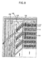
- Fig. 8 illustrates a portion of an organic electro-luminescence display device according to a second embodiment of the present invention
- Fig. 9 is a section view of the organic electro-luminescence display device taken along the III-III' and IV-IV' lines in Fig. 8 .
- the EL display device includes a display area P1 provided with an organic EL array having an anode electrode, etc., and a non-display area P2 provided with a pad portion for applying driving signals to the driving electrodes at the display area P1.
- the display area P1 is provided with an anode electrode 104 formed on a substrate 102, and a cathode electrode 112 formed in a direction crossing the anode electrode 104.
- a plurality of anode electrodes 104 are provided on the substrate 102 in such a manner to be spaced at a desired distance from each other.
- An insulting film 106 having an aperture for defining a light-emitting area for each EL cell area and a contact hole 175 for exposing a second line 152 is formed on the substrate 102 provided with the anode electrode 104.
- a barrier rib 108 having an overhang structure in which the upper portion thereof has a larger width than the lower portion thereof is provided on the insulating film 106.
- the barrier rib 108 plays a role to disconnect an organic light-emitting layer 110 to be formed thereon from a cathode line 112.
- the organic light-emitting layer 110 made from an organic compound and the cathode electrode 112 are entirely deposited sequentially on the insulating film 106 provided with the barrier rib 108.
- the organic light-emitting layer 110 is formed by disposing a hole carrier layer, a light-emitting layer and an electron carrier layer onto the insulating film 6.
- the non-display area P2 is provided with a first line (not shown) extended from the anode electrode 104 at the display area P1, data pads for supplying data voltages, via the first line, to the anode electrode 104, a second line 152 connected to the cathode electrode 112, and scan pads for supplying scan voltages via the second line 152.
- the cathode electrode 112 is connected, via the contact hole 175 passing through the insulating film 106, to the second line 52.
- the second line 152 consists of a double layer having a transparent conductive layer 152a and an opaque conductive layer 152b.
- the data pad is connected to a tape carrier package (TCP) mounted with a first driving circuit for generating data voltages to thereby supply the data voltage to each anode voltage 104.
- TCP tape carrier package
- the scan pad is provided at each side of the data pad.
- the scan pad is connected to a TCP mounted with a second driving circuit for generating scan voltages to thereby supply the scan voltage to each cathode electrode 112.
- the non-display area P2 is provided with a dummy barrier rib 109 connected to each of the barrier ribs positioned at the display area P1, and with a dummy insulating pattern 206 formed between the sealant 125 and the dummy barrier rib 109 in such a manner to have concave and convex portions.
- the dummy barrier rib 109 is provided between the organic EL array and the sealant 125, thereby preventing the sealant 125 from being flown into the organic EL array along with the barrier rib 109 positioned at the display area P1.
- the dummy insulating pattern 206 plays a role to partially expose the second line 152 through a concave area 206a and prevent the sealant 125 from being flown into the organic EL array.
- the sealant 125 is dipped into the concave area 206a of the dummy insulating pattern 206 having a height of about 1 to 2 ⁇ m at the non-display area P2, thereby preventing the sealant 125 from being flown into the organic EL array.
- Fig. 10A to Fig. 10F are views for sequentially explaining a method of fabricating the organic EL display device according to the second embodiment of the present invention.
- the anode electrode 104 and the transparent conductive layer 152a are provided by depositing a metal transparent conductive material onto the substrate 102 made from a sodalime or a vulcanized glass and then patterning it by the photolithography and the etching process.
- a metal transparent conductive material such as indium-tin-oxide (ITO) or SnO 2 is used as the metal material.
- the opaque conductive layer 152b is provided by forming an opaque conductive material on the substrate 102 provided with the anode electrode 104 and the transparent conductive layer 152a and patterning it by the photolithography and the etching process.
- the second line 152 that is a double layer of the transparent conductive layer 152a and the opaque conductive layer 152b.
- the insulating film 106 having the contact hole 175 exposing the light-emitting area of the display area P1 and exposing the second line 152 of the non-display area P2 is provided by coating a photosensitive insulating material onto the substrate 102 provided with the second line 152 by the spin coating technique and then patterning it by the photolithography and the etching process. Further, the dummy insulating pattern 206 positioned at the outer area of the insulating film 106 and having concave and convex portions is provided.
- the barrier rib 108 and the dummy barrier rib 109 are provided by depositing a photosensitive organic material onto the insulating film 106 by the photolithography and the etching process.
- the barrier rib 108 is provided at a non-emitting area in such a manner to cross a plurality of anode electrodes 104 in order to divide the pixels, and the dummy barrier rib 109 is connected to each of the barrier rib 108 at the display area P1 and is positioned at the non-display area P1.
- the barrier rib 108 and the dummy barrier rib 109 are provided in such a manner to connect each other, thereby enclosing the organic EL array.
- the organic light-emitting layer 110 is formed on the substrate 102 provided with the barrier rib 108.
- the cathode electrode 112 formed in parallel to the barrier rib 108 and connected to the second line 152 exposed through the contact hole 175 is provided by depositing a metal material onto the substrate 102 provided with the organic light-emitting layer 110.
- the organic EL display device includes the dummy barrier rib 109 connected to each of the barrier ribs 108 at the display area P1 and located between the sealant 125 and the organic EL array.
- the dummy barrier rib 109 plays a role to prevent the sealant 125 from being flown into the organic EL array, along with the barrier rib 108 during the encapsulation process.
- the dummy insulating pattern 206 having concave and convex portions is provided between the sealant 125 and the organic EL array, thereby dipping the sealant 125 flown into the organic EL array into the concave area 206a of the dummy insulating pattern 206.
- the dummy barrier rib connected to each barrier rib and positioned at the non-display area is provided. Accordingly, a damage of the organic EL array caused by the sealant used when the cap is joined with the substrate can be prevented and hence a deterioration of light-emission efficiency and picture quality can be prevented.
- the insulating film having concave and convex portions is provided between the sealant and the dummy barrier rib at the display area. Accordingly, a damage of the organic EL array caused by the sealant used when the cap is joined with the substrate can be prevented and hence a deterioration of light-emission efficiency and picture quality can be prevented.
Abstract
Description
- This invention relates to an electro-luminescence display (ELD), and more particularly to an organic electro-luminescence display device and a fabricating method thereof that are adaptive for preventing a deterioration of light-emission efficiency and picture quality.
-
US 2003/080 678 Al shows an organic electro-luminescence display device comprising an organic electro-luminescence array having first electrodes and second electrodes provided on a substrate with an organic light-emitting layer therebetween, and a separator layer. A barrier portion is provided to enclose the organic electro-luminescent array completely. The device further comprises a cap joined with the substrate by a sealant to package the organic electro-luminescent array.
Recently, there have been developed various flat panel display devices reduced in weight and bulk that is capable of eliminating disadvantages of a cathode ray tube (CRT). Such flat panel display devices include a liquid crystal display (LCD), a field emission display (FED), a plasma display panel (PDP) and an electro-luminescence (EL) display, etc. - There have been actively processed studies for attempting to make a high display quality and a large-dimension screen of the flat panel display device. In such flat panel display devices, the EL display device is a self-luminous device capable of light-emitting for himself.
- The EL display device excites a phosphorous material using carriers such as electrons and holes, thereby displaying a video image.
- The EL display device is largely classified into an inorganic EL display device and an organic EL display device depending upon the used material.
- Since the organic EL display device is driven with a lower voltage (i.e., about 5 to 20V) than the inorganic EL display device requiring a high voltage of 100 to 200V, it permits a direct current low voltage driving. Also, since the organic EL display device has excellent characteristics such as a wide viewing angle, a fast response and a high contrast ratio, etc., it can be used for a pixel of a graphic display, or a pixel of a television image display or a surface light source. Further, the organic EL display device is a device suitable for a post generation flat panel display because it has a thin thickness, a light weight and an excellent color sense.
-
Fig. 1 is a schematic view showing a structure of a general organic EL display device, andFig. 2 is a detailed plan view of a portion (A area) inFig. 1 .Fig. 3 is a section view of the portion of the organic El display device taken along the I -I ' and II-II' lines inFig. 2 . - Referring to
Fig. 1 to Fig. 3 , the related art EL display device includes a display area P1 provided with an organic EL array having driving electrodes (e.g., an anode electrode and a cathode electrode), etc., and a non-display area P2 provided with apad portion 25 for applying driving signals to the driving electrodes at the display area P1. - The display area P1 is provided with an
anode electrode 4 formed on asubstrate 2, and acathode electrode 12 formed in a direction crossing theanode electrode 4. - A plurality of
anode electrodes 4 are provided on thesubstrate 2 in such a manner to be spaced at a desired distance from each other. Aninsulting film 6 having an aperture for each EL cell area is formed on thesubstrate 2 provided with theanode electrode 4. On theinsulating film 6, abarrier rib 8 for making a separation of an organic light-emittinglayer 10 and acathode electrode 12 to be formed thereon is provided. Thebarrier rib 8 is formed in a direction crossing theanode electrode 4, and has an overhang structure in which the upper portion thereof has a larger width than the lower portion thereof. The organic light-emittinglayer 10 made from an organic compound and thecathode electrode 12 are entirely deposited onto theinsulating film 6 provided with thebarrier rib 8. The organic light-emittinglayer 10 is formed by depositing a hole carrier layer, a light-emitting layer and an electron carrier layer onto theinsulating film 6. - The non-display area P2 is provided with a
first line 54 extended from theanode electrode 4 at the display area P1, data pads for supplying data voltages, via thefirst line 54, to theanode electrode 4, asecond line 52 connected to thecathode electrode 12, and scan pads for supplying scan voltages via thesecond line 52. Herein, thesecond line 52 consists of a double layer having a transparentconductive layer 52a and an opaqueconductive layer 52b. The data pad is connected to a tape carrier package (TCP) mounted with a first driving circuit for generating data voltages to thereby supply the data voltage to eachanode voltage 4. The scan pad is provided at each side of the data pad. The scan pad is connected to a TCP mounted with a second driving circuit for generating scan voltages to thereby supply the scan voltage to eachcathode electrode 12. - The organic EL array at the display area P1 has a characteristic liable to be deteriorated against moisture and oxygen. In order to overcome this problem, an encapsulating process is carried out to join the
substrate 2 provided with the organic EL array of theanode electrode 2, etc. with acap 28 by asealant 25 such as an epoxy resin. A getter for absorbing the moisture and oxygen is filled into the rear center portion of thecap 28 to thereby protect an organic EL array from the oxygen and moisture. - In the related art organic EL display device having the structure as mentioned above, as shown in
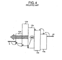
Fig. 4 , if a voltage is applied between theanode electrode 4 and thecathode electrode 12, then electrons (or cathodes) generated from thecathode electrode 12 are moved, via anelectron injection layer 10a and anelectron carrier layer 10b, into a light-emitting layer 10c. On the other hand, holes (or anodes) generated from theanode electrode 4 are moved, via ahole injection layer 10d and ahole carrier layer 10e, into the light-emittinglayer 10c. Thus, electrons and holes fed from theelectron carrier layer 10b and thehole carrier layer 10e are collided with each other to be re-combined at the light-emittinglayer 10c, thereby generating a light. This light is emitted into the exterior via theanode electrode 4, thereby displaying a picture. - Meanwhile, in such an organic EL display device, the
sealant 25 may be frequently flown, via between thebarrier rib 8 and thebarrier rib 8, into the organic EL array of the display area P1 when thecap 28 is joined with thecap 2. Thesealant 25 contains a large amount of moisture, oxygen and impurity to cause a damage to the organic light-emittinglayer 10 of the organic EL array. Therefore, there is raised a problem in that a light-emission efficiency and a picture quality are deteriorated. Further prior art is known fromUS 2003/042852 A1 ,US 5 742 129 A andUS 2003/218 419 A1 . - Accordingly, it is an object of the present invention to provide an organic electro-luminescence display device and a fabricating method thereof that are adaptive for preventing a deterioration of light-emission efficiency and picture quality.
- In order to achieve these and other objects of the invention, an organic electro-luminescence display device according to one aspect of the present invention includes an organic electro-luminescence array having first and second electrodes provided on a substrate with having an organic light-emitting layer therebetween and a barrier rib parallel to any one of the first and second electrodes; and a dummy barrier rib connected to each of the barrier ribs and provided in such a manner to enclose the organic electro-luminescence array along with the barrier rib.
- The organic electro-luminescence display device further includes a cap joined with the substrate by a sealant to package the organic electro-luminescence array.
- In the organic electro-luminescence display device, the sealant is positioned at the outer areas of the barrier rib and the dummy barrier rib.
- The organic electro-luminescence display device further includes a signal supply pad for supplying a driving signal to the organic electro-luminescence array; and a signal line for electrically connecting any one of the first and second electrodes to the signal supply pad.
- The organic electro-luminescence display device further includes an insulating film for exposing a light-emitting area at the first electrode and for exposing the signal line, wherein any one of the first and second electrodes is connected, via said contact hole, to the signal line.
- An organic electro-luminescence display device, in which a substrate provided with an organic electro-luminescence array is joined with a cap by a sealant in order to package the organic electro-luminescence array, according to another aspect of the present invention includes a first insulating pattern positioned between the organic electro-luminescence array and the sealant and provided in such a manner to have concave and convex portions.
- In the organic electro-luminescence display device, the organic electro-luminescence array includes first and second electrodes provided on a substrate with having an organic light-emitting layer therebetween; and a barrier rib being parallel to any one of the first and second electrodes.
- The organic electro-luminescence display device further includes a signal supply pad for supplying a driving signal to the organic electro-luminescence array; and a signal line for electrically connecting any one of the first and second electrodes to the signal supply pad.
- The organic electro-luminescence display device further includes a second insulating pattern having a contact hole for exposing a light-emitting area at the first electrode and for exposing the signal line, wherein any one of the first and second electrodes is connected, via said contact hole, to the signal line.
- A method of fabricating an organic electro-luminescence display device, in which a substrate provided with an organic electro-luminescence array is joined with a cap by a sealant in order to package the organic electro-luminescence array, according to still another aspect of the present invention includes the step of forming a first insulating pattern positioned between the organic electro-luminescence array and the sealant and provided in such a manner to have concave and convex portions.
- These and other objects of the invention will be apparent from the following detailed description of the embodiments of the present invention with reference to the accompanying drawings, in which:
-
Fig. 1 is a schematic view showing a structure of a related art organic electro-luminescence display device; -
Fig. 2 is a detailed view of the A area of the organic electro-luminescence display device shown inFig. 1 ; -
Fig. 3 is a section view of the portion of the organic El display device taken along the I -I ' and II -II' lines inFig. 2 ; -
Fig. 4 is a diagram for explaining a light-emitting principle of the related art organic electro-luminescence display device; -
Fig. 5 illustrates a portion of an organic electro-luminescence display device according to a first embodiment of the present invention; -
Fig. 6 is a section view of the organic electro-luminescence display device taken along the III-III' and IV-IV' lines inFig. 5 ; -
Fig. 7A to Fig. 7F are section views for sequentially explaining a method of fabricating the organic electro-luminescence display device shown inFig. 6 ; -
Fig. 8 illustrates a portion of an organic electro-luminescence display device according to a second embodiment of the present invention; -
Fig. 9 is a section view of the organic electro-luminescence display device taken along the III -III ' and IV-IV' lines inFig. 8 ; and -
Fig. 10A to Fig. 10F are section views for sequentially explaining a method of fabricating the organic electro-luminescence display device shown inFig. 8 . - Reference will now be made in detail to the preferred embodiments of the present invention, examples of which are illustrated in the accompanying drawings.
- Hereinafter, the preferred embodiment of the present invention will be described in detail with reference to
Figs. 5 to 10F . -
Fig. 5 shows a portion of an organic electro-luminescence display device according to a first embodiment of the present invention, andFig. 6 is a section view of the organic electro-luminescence display device taken along the III-III' and IV-IV' lines inFig. 5 . - Referring to
Fig. 5 andFig. 6 , the EL display device includes a display area P1 provided with an organic EL array having an anode electrode, etc., and a non-display area P2 provided with a pad portion for applying driving signals to the driving electrodes at the display area P1. - The display area P1 is provided with an
anode electrode 104 formed on asubstrate 102, and acathode electrode 112 formed in a direction crossing theanode electrode 104. - A plurality of
anode electrodes 104 are provided on thesubstrate 102 in such a manner to be spaced at a desired distance from each other. Aninsulting film 106 having an aperture for defining a light-emitting area for each EL cell area and acontact hole 175 for exposing asecond line 152 is formed on thesubstrate 102 provided with theanode electrode 104. Abarrier rib 108 having an overhang structure in which the upper portion thereof has a larger width than the lower portion thereof is provided on the insulatingfilm 106. - The
barrier rib 108 plays a role to disconnect an organic light-emittinglayer 110 to be formed thereon from acathode line 112. - The organic light-emitting
layer 110 made from an organic compound and thecathode electrode 112 are entirely deposited sequentially on the insulatingfilm 106 provided with thebarrier rib 108. The organic light-emittinglayer 110 is formed by disposing a hole carrier layer, a light-emitting layer and an electron carrier layer onto the insulatingfilm 6. - The non-display area P2 is provided with a first line (not shown) extended from the
anode electrode 104 at the display area P1, data pads for supplying data voltages, via the first line, to theanode electrode 104, asecond line 152 connected to thecathode electrode 112, and scan pads for supplying scan voltages via thesecond line 152. Herein, thecathode electrode 112 is connected, via thecontact hole 175 passing through the insulatingfilm 106, to thesecond line 52. Thesecond line 152 consists of a double layer having a transparentconductive layer 152a and an opaqueconductive layer 152b. - The data pad is connected to a tape carrier package (TCP) mounted with a first driving circuit for generating data voltages to thereby supply the data voltage to each
anode voltage 104. The scan pad is provided at each side of the data pad. The scan pad is connected to a TCP mounted with a second driving circuit for generating scan voltages to thereby supply the scan voltage to eachcathode electrode 112. - Further, the non-display area P2 is provided with a
dummy barrier rib 109 connected to each of the barrier ribs positioned at the display area P1. Thedummy barrier rib 109 plays a role to protect the organic EL array from thesealant 125 used when thesubstrate 102 is joined with thecap 128 along with thebarrier rib 108 at the display area P1. In other words, thedummy barrier rib 109 is provided between the organic EL array and thesealant 125, thereby preventing thesealant 125 from being flown into the organic EL array. - This prevents a damage of the organic light-emitting layer of the organic EL array caused by the
sealant 125 during the encapsulation process, thereby preventing a deterioration of light-emission efficiency and picture quality. -
Fig. 7A to Fig. 7F are views for sequentially explaining a method of fabricating the organic EL display device according to the first embodiment of the present invention. - Firstly, as shown in
Fig. 7A , theanode electrode 104 and the transparentconductive layer 152a are provided by depositing a metal transparent conductive material onto thesubstrate 102 made from a sodalime or a vulcanized glass and then patterning it by the photolithography and the etching process. Herein, indium-tin-oxide (ITO) or SnO2 is used as the metal material. - As shown in
Fig. 7B , the opaqueconductive layer 152b is provided by forming an opaque conductive material on thesubstrate 102 provided with theanode electrode 104 and the transparentconductive layer 152a and patterning it by the photolithography and the etching process. Thus, there is provided thesecond line 152 that is a double layer of the transparentconductive layer 152a and the opaqueconductive layer 152b. - As shown in
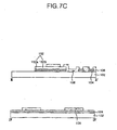
Fig. 7C , the insulatingfilm 106 having thecontact hole 175 exposing the light-emitting area of the display area P1 and exposing thesecond line 152 of the non-display area P2 is provided by coating a photosensitive insulating material onto thesubstrate 102 provided with thesecond line 152 by the spin coating technique and then patterning it by the photolithography and the etching process. - As shown in
Fig. 7D , thebarrier rib 108 and thedummy barrier rib 109 are provided by depositing a photosensitive organic material onto the insulatingfilm 106 by the photolithography and the etching process. Thebarrier rib 108 is provided at a non-emitting area in such a manner to cross a plurality ofanode electrodes 104 in order to divide the pixels, and thedummy barrier rib 109 is connected to each of thebarrier rib 108 at the display area P1 and is positioned at the non-display area P1. Herein, thebarrier rib 108 and thedummy barrier rib 109 are provided in such a manner to connect each other, thereby enclosing the organic EL array. - As shown in
Fig. 7E , the organic light-emittinglayer 110 is formed on thesubstrate 102 provided with thebarrier rib 108. - As shown in
Fig. 7F , thecathode electrode 112 formed in parallel to thebarrier rib 108 and connected to thesecond line 152 exposed through thecontact hole 175 is provided by depositing a metal material onto thesubstrate 102 provided with the organic light-emittinglayer 110. - As described above, the organic EL display device according to the first embodiment of the present invention includes the
dummy barrier rib 109 connected to each of thebarrier ribs 108 at the display area P1 and located between thesealant 125 and the organic EL array. Thus, the organic EL array provided at the display area P1 is enclosed by thebarrier rib 108 and thedummy barrier rib 109, so that it becomes possible to prevent thesealant 125 from being flown into the organic EL array. As a result, a damage of the organic light-emittinglayer 110 can be prevented and hence a deterioration of light-emission efficiency and picture quality can be prevented. -
Fig. 8 illustrates a portion of an organic electro-luminescence display device according to a second embodiment of the present invention, andFig. 9 is a section view of the organic electro-luminescence display device taken along the III-III' and IV-IV' lines inFig. 8 . - Referring to
Fig. 8 andFig. 9 , the EL display device includes a display area P1 provided with an organic EL array having an anode electrode, etc., and a non-display area P2 provided with a pad portion for applying driving signals to the driving electrodes at the display area P1. - The display area P1 is provided with an
anode electrode 104 formed on asubstrate 102, and acathode electrode 112 formed in a direction crossing theanode electrode 104. - A plurality of
anode electrodes 104 are provided on thesubstrate 102 in such a manner to be spaced at a desired distance from each other. Aninsulting film 106 having an aperture for defining a light-emitting area for each EL cell area and acontact hole 175 for exposing asecond line 152 is formed on thesubstrate 102 provided with theanode electrode 104. Abarrier rib 108 having an overhang structure in which the upper portion thereof has a larger width than the lower portion thereof is provided on the insulatingfilm 106. - The
barrier rib 108 plays a role to disconnect an organic light-emittinglayer 110 to be formed thereon from acathode line 112. - The organic light-emitting
layer 110 made from an organic compound and thecathode electrode 112 are entirely deposited sequentially on the insulatingfilm 106 provided with thebarrier rib 108. The organic light-emittinglayer 110 is formed by disposing a hole carrier layer, a light-emitting layer and an electron carrier layer onto the insulatingfilm 6. - The non-display area P2 is provided with a first line (not shown) extended from the
anode electrode 104 at the display area P1, data pads for supplying data voltages, via the first line, to theanode electrode 104, asecond line 152 connected to thecathode electrode 112, and scan pads for supplying scan voltages via thesecond line 152. Herein, thecathode electrode 112 is connected, via thecontact hole 175 passing through the insulatingfilm 106, to thesecond line 52. Thesecond line 152 consists of a double layer having a transparentconductive layer 152a and an opaqueconductive layer 152b. - The data pad is connected to a tape carrier package (TCP) mounted with a first driving circuit for generating data voltages to thereby supply the data voltage to each
anode voltage 104. The scan pad is provided at each side of the data pad. The scan pad is connected to a TCP mounted with a second driving circuit for generating scan voltages to thereby supply the scan voltage to eachcathode electrode 112. - Further, the non-display area P2 is provided with a
dummy barrier rib 109 connected to each of the barrier ribs positioned at the display area P1, and with adummy insulating pattern 206 formed between thesealant 125 and thedummy barrier rib 109 in such a manner to have concave and convex portions. - The
dummy barrier rib 109 is provided between the organic EL array and thesealant 125, thereby preventing thesealant 125 from being flown into the organic EL array along with thebarrier rib 109 positioned at the display area P1. - The
dummy insulating pattern 206 plays a role to partially expose thesecond line 152 through aconcave area 206a and prevent thesealant 125 from being flown into the organic EL array. - In other words, even though a portion of the
sealant 125 is moved toward the organic EL array when thesubstrate 102 is joined with thecap 128 for the purpose of packaging the organic EL array, thesealant 125 is dipped into theconcave area 206a of thedummy insulating pattern 206 having a height of about 1 to 2µm at the non-display area P2, thereby preventing thesealant 125 from being flown into the organic EL array. - This prevents a damage of the organic light-emitting layer of the organic EL array caused by the
sealant 125 during the encapsulation process, thereby preventing a deterioration of light-emission efficiency and picture quality. -
Fig. 10A to Fig. 10F are views for sequentially explaining a method of fabricating the organic EL display device according to the second embodiment of the present invention. - Firstly, as shown in
Fig. 10A , theanode electrode 104 and the transparentconductive layer 152a are provided by depositing a metal transparent conductive material onto thesubstrate 102 made from a sodalime or a vulcanized glass and then patterning it by the photolithography and the etching process. Herein, indium-tin-oxide (ITO) or SnO2 is used as the metal material. - As shown in
Fig. 10B , the opaqueconductive layer 152b is provided by forming an opaque conductive material on thesubstrate 102 provided with theanode electrode 104 and the transparentconductive layer 152a and patterning it by the photolithography and the etching process. Thus, there is provided thesecond line 152 that is a double layer of the transparentconductive layer 152a and the opaqueconductive layer 152b. - As shown in
Fig. 10C , the insulatingfilm 106 having thecontact hole 175 exposing the light-emitting area of the display area P1 and exposing thesecond line 152 of the non-display area P2 is provided by coating a photosensitive insulating material onto thesubstrate 102 provided with thesecond line 152 by the spin coating technique and then patterning it by the photolithography and the etching process. Further, thedummy insulating pattern 206 positioned at the outer area of the insulatingfilm 106 and having concave and convex portions is provided. - As shown in
Fig. 10D , thebarrier rib 108 and thedummy barrier rib 109 are provided by depositing a photosensitive organic material onto the insulatingfilm 106 by the photolithography and the etching process. Thebarrier rib 108 is provided at a non-emitting area in such a manner to cross a plurality ofanode electrodes 104 in order to divide the pixels, and thedummy barrier rib 109 is connected to each of thebarrier rib 108 at the display area P1 and is positioned at the non-display area P1. Herein, thebarrier rib 108 and thedummy barrier rib 109 are provided in such a manner to connect each other, thereby enclosing the organic EL array. - As shown in
Fig. 10E , the organic light-emittinglayer 110 is formed on thesubstrate 102 provided with thebarrier rib 108. - As shown in
Fig. 10F , thecathode electrode 112 formed in parallel to thebarrier rib 108 and connected to thesecond line 152 exposed through thecontact hole 175 is provided by depositing a metal material onto thesubstrate 102 provided with the organic light-emittinglayer 110. - As described above, the organic EL display device according to the second embodiment of the present invention includes the
dummy barrier rib 109 connected to each of thebarrier ribs 108 at the display area P1 and located between thesealant 125 and the organic EL array. Thedummy barrier rib 109 plays a role to prevent thesealant 125 from being flown into the organic EL array, along with thebarrier rib 108 during the encapsulation process. Further, thedummy insulating pattern 206 having concave and convex portions is provided between thesealant 125 and the organic EL array, thereby dipping thesealant 125 flown into the organic EL array into theconcave area 206a of thedummy insulating pattern 206. This prevents thesealant 125 from being flown into the organic EL array. Accordingly, a damage of the organic light-emittinglayer 110 caused by thesealant 125 can be prevented and hence a deterioration of light-emission efficiency and picture quality can be prevented. - As described above, according to the present invention, the dummy barrier rib connected to each barrier rib and positioned at the non-display area is provided. Accordingly, a damage of the organic EL array caused by the sealant used when the cap is joined with the substrate can be prevented and hence a deterioration of light-emission efficiency and picture quality can be prevented.
- Furthermore, according to the present invention, the insulating film having concave and convex portions is provided between the sealant and the dummy barrier rib at the display area. Accordingly, a damage of the organic EL array caused by the sealant used when the cap is joined with the substrate can be prevented and hence a deterioration of light-emission efficiency and picture quality can be prevented.
- Although the present invention has been explained by the embodiments shown in the drawings described above, it should be understood to the ordinary skilled person in the art that the invention is not limited to the embodiments, but rather that various changes or modifications thereof are possible without departing from the scope of the appended claims.
Claims (5)
- An organic electro-luminescence display device, comprising:an organic electro-luminescence array having first electrodes (104) and second electrodes (112) provided on a substrate (102), organic light-emitting layers (110) therebetween and barrier ribs (108) provided at the display area (P1) and parallel to the first (104) or second (112) electrodes;a dummy barrier rib (109) provided at the non-display area (P2) and in such a manner to enclose the organic electro-luminescence array along with the barrier ribs (108), anda cap (128) joined with the substrate (102) by a sealant (125) to package the organic electro-luminescence array,
characterized in thatthe dummy barrier rib (109) is connected to each of the barrier ribs (108), thereby preventing the sealant from being flown into the organic light-emitting layers. - The organic electro-luminescence display device according to claim 1, wherein the sealant (125) is positioned at the outer areas of the barrier rib (108) and the dummy barrier rib (109).
- The organic electro-luminescence display device according to claim 1, further comprising:a signal supply pad for supplying a driving signal to the organic electro-luminescence array; anda signal line (152) for electrically connecting any one of the first (104) and second (112) electrodes to the signal supply pad.
- The organic electro-luminescence display device according to claim 3, further comprising:an insulating film (106) having a contact hole (175) for exposing the signal line (152) and an aperture for exposing a light-emitting area at the first electrode (104),wherein any one of the first (104) and second (112) electrodes is connected, via said contact hole (175), to the signal line (152).
- The organic electro-luminescence display device according to claim 1, further comprising:a first insulating pattern positioned between the organic electro-luminescence array and the sealant (125) and provided in such a manner to have concave and convex portions.
Applications Claiming Priority (4)
| Application Number | Priority Date | Filing Date | Title |
|---|---|---|---|
| KR2004031001 | 2004-05-03 | ||
| KR2004031000 | 2004-05-03 | ||
| KR1020040031000A KR100638139B1 (en) | 2004-05-03 | 2004-05-03 | Organic Electro-Luminescence Display Device And Fabricating Method Thereof |
| KR1020040031001A KR100641733B1 (en) | 2004-05-03 | 2004-05-03 | Organic Electro-Luminescence Display Device And Fabricating Method Thereof |
Publications (3)
| Publication Number | Publication Date |
|---|---|
| EP1594177A2 EP1594177A2 (en) | 2005-11-09 |
| EP1594177A3 EP1594177A3 (en) | 2006-05-17 |
| EP1594177B1 true EP1594177B1 (en) | 2011-09-14 |
Family
ID=34936072
Family Applications (1)
| Application Number | Title | Priority Date | Filing Date |
|---|---|---|---|
| EP05009663A Active EP1594177B1 (en) | 2004-05-03 | 2005-05-03 | Organic electro-luminescence display device and fabricating method thereof |
Country Status (4)
| Country | Link |
|---|---|
| US (2) | US7560861B2 (en) |
| EP (1) | EP1594177B1 (en) |
| JP (1) | JP5181226B2 (en) |
| AT (1) | ATE524840T1 (en) |
Families Citing this family (9)
| Publication number | Priority date | Publication date | Assignee | Title |
|---|---|---|---|---|
| US7358526B2 (en) * | 2005-09-28 | 2008-04-15 | Osram Opto Semiconductors Gmbh | OLED separating structures |
| JP4466550B2 (en) * | 2005-12-08 | 2010-05-26 | ソニー株式会社 | Display device |
| WO2007114536A1 (en) * | 2006-04-05 | 2007-10-11 | Daewoo Electronics Corporation | Organic electroluminescence device and method for manufacturing same |
| US8283853B2 (en) * | 2010-03-31 | 2012-10-09 | General Electric Company | Light-emitting device and article |
| KR101881083B1 (en) * | 2011-11-09 | 2018-07-24 | 삼성디스플레이 주식회사 | Organic light emitting display device |
| KR101484681B1 (en) * | 2012-11-01 | 2015-01-20 | 엘지디스플레이 주식회사 | Organic light emitting display device |
| EP2731138B1 (en) * | 2012-11-09 | 2020-06-17 | EM Microelectronic-Marin SA | Method for manufacturing an OLED display, resulting OLED display and timepiece including such a display |
| KR102376966B1 (en) | 2015-08-11 | 2022-03-22 | 삼성디스플레이 주식회사 | Display apparatus and method of manufacturing the same |
| KR102333549B1 (en) * | 2017-07-05 | 2021-11-30 | 엘지디스플레이 주식회사 | Display device |
Citations (2)
| Publication number | Priority date | Publication date | Assignee | Title |
|---|---|---|---|---|
| US5742129A (en) * | 1995-02-21 | 1998-04-21 | Pioneer Electronic Corporation | Organic electroluminescent display panel with projecting ramparts and method for manufacturing the same |
| US20030218419A1 (en) * | 2002-05-21 | 2003-11-27 | Bae Sung Joon | Electroluminescence display device and method of fabricating the same |
Family Cites Families (14)
| Publication number | Priority date | Publication date | Assignee | Title |
|---|---|---|---|---|
| JPH07169567A (en) * | 1993-12-16 | 1995-07-04 | Idemitsu Kosan Co Ltd | Organic el element |
| JP4114895B2 (en) | 1998-07-08 | 2008-07-09 | Tdk株式会社 | Organic EL display device |
| JP4279391B2 (en) | 1999-02-16 | 2009-06-17 | 東北パイオニア株式会社 | Light emitting display panel and manufacturing method thereof |
| US6582504B1 (en) | 1999-11-24 | 2003-06-24 | Sharp Kabushiki Kaisha | Coating liquid for forming organic EL element |
| US6781309B2 (en) * | 2000-11-29 | 2004-08-24 | Cld, Inc. | Plasma switched organic electroluminescent display |
| JP2002329576A (en) | 2001-04-27 | 2002-11-15 | Semiconductor Energy Lab Co Ltd | Light emitting device and its manufacturing method |
| WO2003019696A2 (en) | 2001-08-25 | 2003-03-06 | Cambridge Display Technology Limited | Electroluminescent device |
| GB2379216A (en) | 2001-08-28 | 2003-03-05 | Maurice Ward Gittos | Piperidin-2,6-dione salts useful for the treatment of stress-related affective disorders |
| JP2003086355A (en) | 2001-09-05 | 2003-03-20 | Kiko Kenji Kagi Kofun Yugenkoshi | Sealing structure, sealing method, and sealing device for organic el element |
| KR100768182B1 (en) | 2001-10-26 | 2007-10-17 | 삼성에스디아이 주식회사 | Organic electro luminescence device and method of manufacturing the same |
| CN1452437A (en) | 2002-04-17 | 2003-10-29 | 朱星厚 | Method for mfg. organic electroluminescent display panel covered with protective film |
| US7193364B2 (en) | 2002-09-12 | 2007-03-20 | Osram Opto Semiconductors (Malaysia) Sdn. Bhd | Encapsulation for organic devices |
| JP3997888B2 (en) * | 2002-10-25 | 2007-10-24 | セイコーエプソン株式会社 | Electro-optical device, method of manufacturing electro-optical device, and electronic apparatus |
| US7154222B2 (en) * | 2003-04-11 | 2006-12-26 | Samsung Sdi Co., Ltd | Plasma display panel having reinforcing barrier ribs with curvature |
-
2005
- 2005-05-02 US US11/118,543 patent/US7560861B2/en active Active
- 2005-05-03 AT AT05009663T patent/ATE524840T1/en not_active IP Right Cessation
- 2005-05-03 EP EP05009663A patent/EP1594177B1/en active Active
- 2005-05-06 JP JP2005135191A patent/JP5181226B2/en active Active
-
2009
- 2009-06-09 US US12/481,351 patent/US7851994B2/en active Active
Patent Citations (2)
| Publication number | Priority date | Publication date | Assignee | Title |
|---|---|---|---|---|
| US5742129A (en) * | 1995-02-21 | 1998-04-21 | Pioneer Electronic Corporation | Organic electroluminescent display panel with projecting ramparts and method for manufacturing the same |
| US20030218419A1 (en) * | 2002-05-21 | 2003-11-27 | Bae Sung Joon | Electroluminescence display device and method of fabricating the same |
Also Published As
| Publication number | Publication date |
|---|---|
| JP5181226B2 (en) | 2013-04-10 |
| US7851994B2 (en) | 2010-12-14 |
| US20050242719A1 (en) | 2005-11-03 |
| US20090243480A1 (en) | 2009-10-01 |
| JP2005322650A (en) | 2005-11-17 |
| ATE524840T1 (en) | 2011-09-15 |
| EP1594177A3 (en) | 2006-05-17 |
| US7560861B2 (en) | 2009-07-14 |
| EP1594177A2 (en) | 2005-11-09 |
Similar Documents
| Publication | Publication Date | Title |
|---|---|---|
| US7851994B2 (en) | Organic electro-luminescence display device with an organic electro-luminescence array and fabricating method thereof | |
| US7518147B2 (en) | Organic electro luminescence device and fabrication method thereof | |
| EP1608032B1 (en) | Organic electro-luminescence display device and fabricating method thereof | |
| US7919919B2 (en) | Organic electroluminescent display having a specific structure for a pad supplying the drive signal | |
| US20050258741A1 (en) | Organic electro-luminescence display device and fabricating method thereof | |
| US7221091B2 (en) | Organic electroluminescent display device and method of fabricating the same | |
| US7183708B2 (en) | Organic electro luminescence display device and fabricating method thereof | |
| US7486018B2 (en) | Organic electro-luminescence display device and fabricating method thereof | |
| US20050218800A1 (en) | Organic electro-luminescence display device and fabricating method thereof | |
| KR20080108743A (en) | Organic electro-luminescence display device and method for fabricating thereof | |
| CN1694594B (en) | Organic electro-luminescence display device and fabricating method thereof | |
| KR100726942B1 (en) | Organic Electro-Luminescence Display Device And Fabricating Method Thereof | |
| KR100623450B1 (en) | Organic Electro-Luminescence Display Device And Fabricating Method Thereof | |
| US20060113896A1 (en) | Organic electro-luminescence display device and fabricating method thereof | |
| KR100641733B1 (en) | Organic Electro-Luminescence Display Device And Fabricating Method Thereof | |
| JP3653942B2 (en) | Organic light emitting device and method for manufacturing the same | |
| KR20030086821A (en) | Method for manufacturing Organic Electro Luminescent Display Device for shaping sub pixel | |
| KR100726939B1 (en) | Organic Electro-Luminescence Display Device And Fabricating Method Thereof |
Legal Events
| Date | Code | Title | Description |
|---|---|---|---|
| PUAI | Public reference made under article 153(3) epc to a published international application that has entered the european phase |
Free format text: ORIGINAL CODE: 0009012 |
|
| 17P | Request for examination filed |
Effective date: 20050503 |
|
| AK | Designated contracting states |
Kind code of ref document: A2 Designated state(s): AT BE BG CH CY CZ DE DK EE ES FI FR GB GR HU IE IS IT LI LT LU MC NL PL PT RO SE SI SK TR |
|
| AX | Request for extension of the european patent |
Extension state: AL BA HR LV MK YU |
|
| PUAL | Search report despatched |
Free format text: ORIGINAL CODE: 0009013 |
|
| AK | Designated contracting states |
Kind code of ref document: A3 Designated state(s): AT BE BG CH CY CZ DE DK EE ES FI FR GB GR HU IE IS IT LI LT LU MC NL PL PT RO SE SI SK TR |
|
| AX | Request for extension of the european patent |
Extension state: AL BA HR LV MK YU |
|
| 17Q | First examination report despatched |
Effective date: 20060823 |
|
| AKX | Designation fees paid |
Designated state(s): AT BE BG CH CY CZ DE DK EE ES FI FR GB GR HU IE IS IT LI LT LU MC NL PL PT RO SE SI SK TR |
|
| RIC1 | Information provided on ipc code assigned before grant |
Ipc: H01L 27/32 20060101ALI20110105BHEP Ipc: H01L 51/52 20060101AFI20110105BHEP |
|
| GRAP | Despatch of communication of intention to grant a patent |
Free format text: ORIGINAL CODE: EPIDOSNIGR1 |
|
| RAP1 | Party data changed (applicant data changed or rights of an application transferred) |
Owner name: LG ELECTRONICS, INC. |
|
| GRAS | Grant fee paid |
Free format text: ORIGINAL CODE: EPIDOSNIGR3 |
|
| GRAA | (expected) grant |
Free format text: ORIGINAL CODE: 0009210 |
|
| AK | Designated contracting states |
Kind code of ref document: B1 Designated state(s): AT BE BG CH CY CZ DE DK EE ES FI FR GB GR HU IE IS IT LI LT LU MC NL PL PT RO SE SI SK TR |
|
| REG | Reference to a national code |
Ref country code: GB Ref legal event code: FG4D |
|
| REG | Reference to a national code |
Ref country code: CH Ref legal event code: EP |
|
| REG | Reference to a national code |
Ref country code: IE Ref legal event code: FG4D |
|
| REG | Reference to a national code |
Ref country code: DE Ref legal event code: R096 Ref document number: 602005029973 Country of ref document: DE Effective date: 20111110 |
|
| REG | Reference to a national code |
Ref country code: NL Ref legal event code: VDEP Effective date: 20110914 |
|
| PG25 | Lapsed in a contracting state [announced via postgrant information from national office to epo] |
Ref country code: LT Free format text: LAPSE BECAUSE OF FAILURE TO SUBMIT A TRANSLATION OF THE DESCRIPTION OR TO PAY THE FEE WITHIN THE PRESCRIBED TIME-LIMIT Effective date: 20110914 Ref country code: FI Free format text: LAPSE BECAUSE OF FAILURE TO SUBMIT A TRANSLATION OF THE DESCRIPTION OR TO PAY THE FEE WITHIN THE PRESCRIBED TIME-LIMIT Effective date: 20110914 Ref country code: SE Free format text: LAPSE BECAUSE OF FAILURE TO SUBMIT A TRANSLATION OF THE DESCRIPTION OR TO PAY THE FEE WITHIN THE PRESCRIBED TIME-LIMIT Effective date: 20110914 |
|
| LTIE | Lt: invalidation of european patent or patent extension |
Effective date: 20110914 |
|
| PG25 | Lapsed in a contracting state [announced via postgrant information from national office to epo] |
Ref country code: CY Free format text: LAPSE BECAUSE OF FAILURE TO SUBMIT A TRANSLATION OF THE DESCRIPTION OR TO PAY THE FEE WITHIN THE PRESCRIBED TIME-LIMIT Effective date: 20110914 Ref country code: SI Free format text: LAPSE BECAUSE OF FAILURE TO SUBMIT A TRANSLATION OF THE DESCRIPTION OR TO PAY THE FEE WITHIN THE PRESCRIBED TIME-LIMIT Effective date: 20110914 Ref country code: AT Free format text: LAPSE BECAUSE OF FAILURE TO SUBMIT A TRANSLATION OF THE DESCRIPTION OR TO PAY THE FEE WITHIN THE PRESCRIBED TIME-LIMIT Effective date: 20110914 Ref country code: GR Free format text: LAPSE BECAUSE OF FAILURE TO SUBMIT A TRANSLATION OF THE DESCRIPTION OR TO PAY THE FEE WITHIN THE PRESCRIBED TIME-LIMIT Effective date: 20111215 |
|
| REG | Reference to a national code |
Ref country code: AT Ref legal event code: MK05 Ref document number: 524840 Country of ref document: AT Kind code of ref document: T Effective date: 20110914 |
|
| PG25 | Lapsed in a contracting state [announced via postgrant information from national office to epo] |
Ref country code: BE Free format text: LAPSE BECAUSE OF FAILURE TO SUBMIT A TRANSLATION OF THE DESCRIPTION OR TO PAY THE FEE WITHIN THE PRESCRIBED TIME-LIMIT Effective date: 20110914 |
|
| PG25 | Lapsed in a contracting state [announced via postgrant information from national office to epo] |
Ref country code: CZ Free format text: LAPSE BECAUSE OF FAILURE TO SUBMIT A TRANSLATION OF THE DESCRIPTION OR TO PAY THE FEE WITHIN THE PRESCRIBED TIME-LIMIT Effective date: 20110914 Ref country code: IS Free format text: LAPSE BECAUSE OF FAILURE TO SUBMIT A TRANSLATION OF THE DESCRIPTION OR TO PAY THE FEE WITHIN THE PRESCRIBED TIME-LIMIT Effective date: 20120114 Ref country code: SK Free format text: LAPSE BECAUSE OF FAILURE TO SUBMIT A TRANSLATION OF THE DESCRIPTION OR TO PAY THE FEE WITHIN THE PRESCRIBED TIME-LIMIT Effective date: 20110914 |
|
| PG25 | Lapsed in a contracting state [announced via postgrant information from national office to epo] |
Ref country code: NL Free format text: LAPSE BECAUSE OF FAILURE TO SUBMIT A TRANSLATION OF THE DESCRIPTION OR TO PAY THE FEE WITHIN THE PRESCRIBED TIME-LIMIT Effective date: 20110914 Ref country code: EE Free format text: LAPSE BECAUSE OF FAILURE TO SUBMIT A TRANSLATION OF THE DESCRIPTION OR TO PAY THE FEE WITHIN THE PRESCRIBED TIME-LIMIT Effective date: 20110914 Ref country code: IT Free format text: LAPSE BECAUSE OF FAILURE TO SUBMIT A TRANSLATION OF THE DESCRIPTION OR TO PAY THE FEE WITHIN THE PRESCRIBED TIME-LIMIT Effective date: 20110914 Ref country code: PT Free format text: LAPSE BECAUSE OF FAILURE TO SUBMIT A TRANSLATION OF THE DESCRIPTION OR TO PAY THE FEE WITHIN THE PRESCRIBED TIME-LIMIT Effective date: 20120116 Ref country code: RO Free format text: LAPSE BECAUSE OF FAILURE TO SUBMIT A TRANSLATION OF THE DESCRIPTION OR TO PAY THE FEE WITHIN THE PRESCRIBED TIME-LIMIT Effective date: 20110914 Ref country code: PL Free format text: LAPSE BECAUSE OF FAILURE TO SUBMIT A TRANSLATION OF THE DESCRIPTION OR TO PAY THE FEE WITHIN THE PRESCRIBED TIME-LIMIT Effective date: 20110914 |
|
| PLBE | No opposition filed within time limit |
Free format text: ORIGINAL CODE: 0009261 |
|
| STAA | Information on the status of an ep patent application or granted ep patent |
Free format text: STATUS: NO OPPOSITION FILED WITHIN TIME LIMIT |
|
| PG25 | Lapsed in a contracting state [announced via postgrant information from national office to epo] |
Ref country code: DK Free format text: LAPSE BECAUSE OF FAILURE TO SUBMIT A TRANSLATION OF THE DESCRIPTION OR TO PAY THE FEE WITHIN THE PRESCRIBED TIME-LIMIT Effective date: 20110914 |
|
| 26N | No opposition filed |
Effective date: 20120615 |
|
| REG | Reference to a national code |
Ref country code: DE Ref legal event code: R097 Ref document number: 602005029973 Country of ref document: DE Effective date: 20120615 |
|
| PG25 | Lapsed in a contracting state [announced via postgrant information from national office to epo] |
Ref country code: MC Free format text: LAPSE BECAUSE OF NON-PAYMENT OF DUE FEES Effective date: 20120531 |
|
| REG | Reference to a national code |
Ref country code: CH Ref legal event code: PL |
|
| PG25 | Lapsed in a contracting state [announced via postgrant information from national office to epo] |
Ref country code: LI Free format text: LAPSE BECAUSE OF NON-PAYMENT OF DUE FEES Effective date: 20120531 Ref country code: CH Free format text: LAPSE BECAUSE OF NON-PAYMENT OF DUE FEES Effective date: 20120531 |
|
| REG | Reference to a national code |
Ref country code: IE Ref legal event code: MM4A |
|
| PG25 | Lapsed in a contracting state [announced via postgrant information from national office to epo] |
Ref country code: ES Free format text: LAPSE BECAUSE OF FAILURE TO SUBMIT A TRANSLATION OF THE DESCRIPTION OR TO PAY THE FEE WITHIN THE PRESCRIBED TIME-LIMIT Effective date: 20111225 Ref country code: IE Free format text: LAPSE BECAUSE OF NON-PAYMENT OF DUE FEES Effective date: 20120503 |
|
| PG25 | Lapsed in a contracting state [announced via postgrant information from national office to epo] |
Ref country code: BG Free format text: LAPSE BECAUSE OF FAILURE TO SUBMIT A TRANSLATION OF THE DESCRIPTION OR TO PAY THE FEE WITHIN THE PRESCRIBED TIME-LIMIT Effective date: 20111214 |
|
| PG25 | Lapsed in a contracting state [announced via postgrant information from national office to epo] |
Ref country code: TR Free format text: LAPSE BECAUSE OF FAILURE TO SUBMIT A TRANSLATION OF THE DESCRIPTION OR TO PAY THE FEE WITHIN THE PRESCRIBED TIME-LIMIT Effective date: 20110914 |
|
| PG25 | Lapsed in a contracting state [announced via postgrant information from national office to epo] |
Ref country code: LU Free format text: LAPSE BECAUSE OF NON-PAYMENT OF DUE FEES Effective date: 20120503 |
|
| PG25 | Lapsed in a contracting state [announced via postgrant information from national office to epo] |
Ref country code: HU Free format text: LAPSE BECAUSE OF FAILURE TO SUBMIT A TRANSLATION OF THE DESCRIPTION OR TO PAY THE FEE WITHIN THE PRESCRIBED TIME-LIMIT Effective date: 20050503 |
|
| REG | Reference to a national code |
Ref country code: FR Ref legal event code: PLFP Year of fee payment: 12 |
|
| REG | Reference to a national code |
Ref country code: FR Ref legal event code: PLFP Year of fee payment: 13 |
|
| REG | Reference to a national code |
Ref country code: FR Ref legal event code: PLFP Year of fee payment: 14 |
|
| REG | Reference to a national code |
Ref country code: DE Ref legal event code: R079 Ref document number: 602005029973 Country of ref document: DE Free format text: PREVIOUS MAIN CLASS: H01L0051520000 Ipc: H10K0050800000 |
|
| PGFP | Annual fee paid to national office [announced via postgrant information from national office to epo] |
Ref country code: FR Payment date: 20230405 Year of fee payment: 19 Ref country code: DE Payment date: 20230405 Year of fee payment: 19 |
|
| PGFP | Annual fee paid to national office [announced via postgrant information from national office to epo] |
Ref country code: GB Payment date: 20230405 Year of fee payment: 19 |