BACKGROUND OF THE INVENTION
-
The present invention relates to a voltage equalizer
for battery elements for equalizing terminal voltages of battery
elements which constitute a battery or the like.
-
In general, a battery including a number of (for example,
about one hundred) battery elements which are connected in
series to each other is installed in an electric vehicle which
is run by a motor or a hybrid vehicle which is run in combination
of an engine and a motor. Then, a voltage equalizer is connected
to the battery in consideration of securement of a charging
capacity, extension of the life of each battery element and
safety. Further, a voltage detector for detecting an abnormal
terminal voltage of each battery element is also connected
to the battery to eliminate a risk of the occurrence of a serious
secondary failure which would be caused by heat and leakage
of fluid which are caused in the event that there occurs a
short circuit in one of the battery elements.
-
Conventionally, as a voltage equalizer of this type,
a voltage equalizer for battery elements is known which was
proposed by the applicant of the present invention and is
disclosed in JP-A-2002-223528. In this voltage equalizer,
a closed circuit is configured by battery elements of one of
a plurality of groups of battery elements which are connected
in series, each of a plurality of secondary windings which
are magnetically connected to each other and each of one of
pluralities of switching elements, and a closed circuit is
configured by battery elements of the other group of battery
elements, primary windings which are magnetically connected
to the secondary windings in a common fashion and the other
plurality of switching elements, whereby the output voltage
of the one of a plurality of groups of battery elements which
are connected in series is equalized by ON/OFF controlling
the one of pluralities of switching elements and the other
plurality of switching elements alternately.
-
Inaddition, as the voltage detector, a voltage detection
circuit for battery elements is known which has already been
proposed by the applicant of the present invention and is
disclosed in JP-2002-357625. This voltage detection circuit
is a voltage detection circuit for battery elements for detecting
a voltage between terminals of each of a plurality of battery
elements which are connected in series to each other which
has a voltage detection means connected between terminals of
each of the plurality of battery elements and adapted to cause
a detection current to flow from an output terminal when a
predetermined voltage is reached and a single detection signal
output means connected via a load resistance to a negative
terminal of a battery element, which is positioned on a minimum
potential side, of the plurality of battery elements which
are connected in series to the output terminal of the voltage
detecting means, whereby a sufficient current for the single
detection signal output means to output a detection signal
can securely be allowed to flow even in the event that any
of the battery elements reaches a predetermined voltage which
is set in advance.
-
In the afore said conventional voltage equalizer (and
the voltage detector), however, there exist the following
problems to be solved.
-
As a first problem, when paying attention to the voltage
equalizer, since energy is temporarily stored in the transformer
and thereafter, a substantial equalization process is carried
out, there still remains a room for improvement from equalization
capability and equalization efficiency (equalization time)
perspectives. In addition, since an equalization process is
performed between all of the battery elements, respectively,
there exists a risk that excessive charging and discharging
currents are generated in case terminal voltages between the
battery elements vary largely.
-
As a second problem, in a case where the voltage detector
is connected in addition to the voltage equalizer, since they
constitute two dedicated devices which are independent from
each other, a configuration is generated in which the two
dedicated devices are combined with the battery elements, and
this calls for increase in cost, enhancement of energy loss
and enlargement of size of the entire system.
-
As a third problem, when paying attention to the voltage
detector, since the terminal voltage of each battery element
is detected through an independent detection circuit, a number
of detection circuits which corresponds to the number of battery
elements are required, and in case the number of battery elements
is increased, this calls for an increase in components cost
in conjunction with a remarkable increase in the number of
components and an increase in production costs in association
with the complexity of circuits. In addition, the size of
the system is also increased, and this constitutes a cause
for the prevention of the effort to save space in an electric
vehicle where components layout space is limited, and wasteful
energy loss is also increased.
SUMMARY OF THE INVENTION
-
The invention was made in view of these situations,
and an object thereof is to provide a voltage equalizer for
battery elements which can solve the problems inherent in the
background art.
-
With a view to solving the problems, according to the
invention, there is provided a voltage equalizer for battery
elements for equalizing terminal voltages of a plurality of
battery elements B... , comprising an equalization processing
circuit 6 having a transformer 2 having, in turn, basic windings
2o... made up of at least a plurality of primary windings 2a...
which correspond, respectively, to the plurality of battery
elements and one or two or more secondary windings 2b... ,
a plurality of switching elements 3... which correspond,
respectively, to the battery elements B... , a plurality of
primary diodes 5a... which correspond, respectively, to the
battery elements B... , and one or two or more secondary diodes
5b... which correspond, respectively, to the secondary windings
2b... to thereby constitute a plurality of primary series
circuits Ca... which can carry current from the battery elements
B... via the corresponding primary diodes 5a... to the primary
windings 2a... , when the respective switching elements 3...
are switched on and one or two or more secondary series circuits
Cb... which can carry current from the secondary windings 2b...
via the secondary diodes 5b... to the battery elements B... ,
when the respective switching elements 3... are switched off,
and a control circuit 7 for ON/OFF controlling the respective
switching elements 3... .
-
By this configuration, when the respective switching
elements 3... are switched on in a synchronized fashion, since
the plurality of primary series circuits Ca... are configured
in which current is carried from the respective battery elements
B... via the corresponding primary diodes 5a... to the respective
primary windings 2a..., the respective primary series circuits
Ca... are connected in parallel to each other, and in the event
that the number of turns of the respective basic windings 2o...
is identical, storage currents Is... flow from the battery
terminals B... of a maximum terminal voltage Vomax to the basic
windings 2o... in association with storage of energy into the
transformer 2. On the other hand, thereafter, when the
respective switching elements 3... are switched off in a
synchronized fashion, since the secondary series circuits Cb...
are configured in which current is carried from the secondary
windings 2b... via the secondary diodes 5b... to the battery
elements B... , emission currents Ir... flow from the secondary
windings 2b... to the battery elements B... of a minimum terminal
voltage Vomin in association with emission of energy from the
transformer 2.
-
In this case, according to preferred embodiments of
the invention, it is desirable that the plurality of battery
elements B... are connected in series to each other. Inaddition,
the basic windings 2o... may be made up of pluralities of primary
windings 2a... and secondary windings 2b... which correspond,
respectively, to the battery elements B... by separating the
primary windings and the secondary windings with intermediate
taps 2oc... . Alternatively, the basic windings 2o... may
be made up of a single winding to be used both for the primary
series circuits Ca... in the corresponding battery elements
B... and the secondary series circuits Cb... in the other battery
elements B... , and an auxiliary winding 2x may be provided
in the transformer 2 for use as a secondary series circuit
Cb in the battery elements B where the secondary series circuit
is not configured depending upon the basic windings 2o.
Furthermore, the basic windings 2o... may be made up of a plurality
of primary windings 2a... which correspond, respectively, to
the battery elements B... and one or two or more secondary
windings 2b... which correspond, respectively, to groups G
of one or two or more groups which results when the plurality
of battery elements B... are so grouped. As this occurs, the
secondary windings 2b... may be utilized at least as part of
the plurality of primary windings 2a... .
-
On one hand, the voltage equalizer 1a may include a
voltage detection unit 11 for detecting a maximum terminal
voltage and/or a minimum terminal voltage of the plurality
(all) of battery elements B... from terminal voltages of the
basic windings 2b or a terminal voltage of a detection winding
2d which is separately provided in the transformer 2. Note
that the minimum terminal voltage Vomin may include a minimum
end-to-end voltage Vxmin of end-to-end voltages of the groups
G... of one or two or more groups which result when the plurality
of battery elements B... are so grouped.
-
In addition, the voltage detection circuit 11 may include
a correction circuit 13 for correcting a voltage detected from
the terminal voltages of the basic windings 2o or the terminal
voltage of the detection winding 2d. The voltage detection
circuit 11 may include a maximum voltage holding circuit 12m
for holding (storing) the maximum terminal voltage Vmax and/or
a minimum voltage holding circuit 12s for holding (storing)
the minimum terminal voltage Vmin. Furthermore, the voltage
detection circuit 11 may include a maximum voltage detection
unit 11m for detecting the maximum terminal voltage Vmax
immediately after the switching elements 3... are switched
on. In addition, the voltage detection circuit 11 may include
a minimum voltage detection unit 11s for detecting a minimum
terminal voltage Vmin immediately before emission currents
Ir... generated in association with emission of energy from
the transformer 2 becomes zero after the switching elements
3... are switched off. In this case, the minimum voltage
detection unit 11s can detect the emission currents Ir...
generated in association with emission of energy from the
transformer 2 after the switching elements 3... are switched
off and then can detect the minimum terminal voltage Vmin at
a timing when the magnitude of the emission currents Ir...
so emitted has reached a predetermined threshold Irs. Note
that by providing the minimum voltage detection unit 11s which
is configured as has been described above, there can be provided
a detection circuit 11 for detecting emission currents generated
in association with emission of energy from the transformer
2 after the switching elements 3... have been switched off,
ON controlling the switching elements 3... at a timing when
a predetermined time Tr has elapsed since the emission currents
Ir... became zero, detecting storage currents generated in
association with storage of energy into the transformer 2 after
the switching elements 3... have been switched on, and OFF
controlling the switching elements 3... at a timing when the
magnitude of the storage currents Is... has reached a
predetermined value Ism. In addition, the minimum voltage
detection unit 11s can obtain in advance through an operation
a predetermined time Ts that is spent until the magnitude of
emission currents generated in association with emission of
energy from the transformer 2 decreases to a predetermined
threshold Irs and can detect the minimum terminal voltage Vmin
at a timing when the predetermined time Ts has elapsed after
the switching elements were switched off.
-
On the other hand, the control circuit 7 can obtain
a difference (a differential voltage Ve) between the maximum
terminal voltage Vmax detected by the voltage detection circuit
11s and the minimum terminal voltage Vmin that can be compared
with the maximum terminal voltage Vmax, so that the ON/OFF
control of the switching elements 3... is stopped so as to
be put in an OFF state when the differential voltage Ve is
equal to or lower than a set value Es which has been set in
advance. In addition, the control circuit 7 can obtain a
difference (a differential voltage Ve) between the maximum
terminal voltage Vmax detected by the voltage detection circuit
11 and the minimum terminal voltage Vmin that can be compared
with the maximum terminal voltage Vmax, so that a switching
frequency fs for ON/OFF controlling the switching elements
3... is set to be low when the differential voltage Ve is large,
whereas the switching frequency fs is set to be high when the
differential voltage Ve is small.
-
On one hand, the voltage equalizer can include an energy
replenishment circuit 22 which configures a closed circuit
by connecting in series a replenishment winding 2s provided
in the transformer 2 for replenishment of energy, a battery
unit Bs for replenishing the replenishment winding 2s with
energy and a replenishment switching unit 21. In this case,
assuming that a maximum terminal voltage of the battery elements
is Vomax, the number of turns of the basic windings is No,
the terminal voltage of the battery unit is Vs and the number
of turns of the replenishment winding is Ns, Vs and/or Ns is
set so as to meet a condition for (Vs/Ns) > (Vomax/No). In addition,
the voltage equalizer can include a control circuit 7 for ON/OFF
controlling the switching elements 3... and the replenishment
switching unit 21 by causing the switching elements 3... and
the replenishment switching unit 21 to synchronize with each
other, or ON/OFF controlling the replenishment switching unit
21 with all of the switching elements 3... being OFF controlled.
Furthermore, the voltage equalizer can include an energy
discharge circuit 26 which configures a closed circuit by
connecting in series a discharge winding 2r provided in the
transformer 2 for discharge of energy, a battery unit Bs adapted
to be charged with energy discharged from the discharge winding
2r and a discharge switching unit 25. In this case, assuming
that the minimum terminal voltage of the battery elements is
Vomin, the number of turns of the basic windings is No, the
terminal voltage of the battery unit is Vs, and the number
of turns of the discharge winding is Nr, Vs and/or Ns is set
so as to meet a condition for (Vs/Nr)<(Vomin/No). In addition,
the voltage equalizer can include a control circuit 7 for ON/OFF
controlling the switching elements 3... and the discharge
switching unit 25 by causing the switching elements and the
discharge switching unit to synchronize with each other in
a reverse state, or ON/OFF controlling the switching elements
3... with the discharge switching unit 25 being ON controlled.
Furthermore, the voltage equalizer Ig, 1h can include the
equalization processing circuit 6 which is configured as a
single module M, whereby a plurality of battery elements B...
which correspond, respectively, to a plurality of modules M
are connected in parallel or in series to each other.
-
According to the
voltage equalizer 1a... according
to the invention which is configured as has been described
above, the following remarkable advantages can be provided.
- (1) When the respective switching elements 3... are switched
on, the storage currents Is... flow from the battery terminals
B... of the maximum terminal voltage Vomax to the basic windings
2o... in association with storage of energy into the transformer
2, whereas, when the respective switching elements 3... are
switched off, the emission currents Ir... flow from the basic
windings 2o... to the battery elements B... of the minimum
terminal voltage Vomin in association with emission of energy
from the transformer 2, whereby the equalizing capability and
the equalizing efficiency can remarkably be enhanced.
- (2) Even in the event that the terminal voltages Vo...
of the battery elements B... vary largely, since the emission
currents Ir... (the storage currents Is...) flow through the
secondary series circuits Cb... (the primary series circuits
Ca...) individually, the generation of an adverse effect that
excessive emission currents Ir... (storage currents Is...)
flow when the equalizing process is being carried out can be
prevented.
- (3) According to the preferred embodiment of the invention,
in the event that the basic windings 2o... are made up of the
pluralities of primary windings 2a... and secondary windings
2b... which correspond, respectively, to the battery elements
B... by separating the primary windings and the secondary
windings with the intermediate taps 2oc... , the basic
equalization processing circuit 6... can easily be configured
without providing an auxiliary winding.
- (4) According to the preferred embodiment of the invention,
in the event that the basic windings 2o... are made up of
the single winding to be used both for the primary series circuits
Ca... in the corresponding battery elements B... and the
secondary series circuits Cb... in the other battery elements
B..., and the auxiliary winding 2x is provided in the transformer
2 for use as a secondary series circuit Cb in the battery elements
B where the secondary series circuit is not configured depending
upon the basic windings 2o, although the auxiliary winding
2x is needed, the basic windings 2o... can be made up of the
single winding having the same number of turns as that of the
primary winding 2a (or the secondary winding 2b).
- (5) Furthermore, according to the preferred embodiment
of the invention, in the event that the basic windings 2o...
are made up of the plurality of primary windings 2a... which
correspond, respectively, to the battery elements B... and
one or two or more secondary windings 2b... which correspond,
respectively, to groups G of one or two or more groups which
results when the plurality of battery elements B... are so
grouped, the voltage equalizer can be applied to a capacitor
such as an electric double layer capacitor which produces no
problem (abnormality) even in the event that the terminal voltage
Vo decreases below the normal voltage, whereby the reduction
in cost, size and enhancement of efficiency of the whole system
can be attempted to be attained by simplifying the circuit
configuration on the side of the secondary windings 2b... .
Note that, as this occurs, the secondary windings 2b... can
be utilized at least as part of the plurality of primary windings
2a... , thereby making it possible to simplify the circuit
configuration further.
- (6) According to the preferred embodiment of the invention,
in the even that the voltage equalizer 1a includes the voltage
detection unit 11 for detecting a maximum terminal voltage
and/or a minimum terminal voltage of the plurality (all) of
battery elements B... from terminal voltages of the basic
windings 2b or a terminal voltage of a detection winding 2d
which is separately provided in the transformer 2, the storage
currents Ir... flow from the battery elements B... of the maximum
terminal voltage Vomax to the basic windings 2c... , when the
respective switching elements 3... are switched on, and when
the respective switching elements 3... . are switched off,
the emission currents Ir... flows from the basic windings 2o...
to the battery elements B... of the minimum terminal voltage
Vomin. Due to this, when the respective switching elements
3... are switched on, the maximum terminal voltage Vmax is
generated in the basic winding 2o or the detection windig 2d,
whereas when the respective switching elements 3 are switched
off, the minimum terminal voltage Vmin is generated in the
basic wiring 2o or the detection winding 2d. Consequently,
the maximum terminal voltage Vmax and the minimum terminal
voltage Vmin can easily be detected, and since the voltage
detection unit 11 doubles as the substantial part of the voltage
equalizer 1, the configuration of the system can be simplified.
Moreover, since, as with the conventional voltage detection
circuits, the necessity of the voltage detection circuits for
detecting the terminal voltages Vo... of the respective battery
elements B... independently can be obviated, the reduction
in cost, energy loss and size of the whole system can be attempted
to be attained. Note that since a main object of the voltage
detection circuit 11 is to detect the battery elements B...
whose terminal voltages Vo... deviate from the normal range
to thereby become extraordinarily low or high, the object can
be sufficiently met when only the maximum terminal voltage
Vmax and the minimum terminal voltage Vmin can be detected,
and therefore, there is no need to detect even normal terminal
voltages Vo... . Consequently, the original object can be
attained to a sufficient extent in the event that the voltage
detection circuit 11 according to the embodiment of the invention
is used which detects only the maximum terminal voltage Vmax
and the minimum terminal voltage Vmin. Note that in the event
that the detection winding 2d is provided separately in the
transformer 2, an electrical insulation relative to the voltage
equalization processing circuit 6 can be attempted, and the
detection voltage can be increased or decreased as required.
- (7) According to the preferred embodiment of the invention,
in the event that the minimum terminal voltage... adopts a
minimum end-to-end voltage Vxmin of end-to-end voltages of
the groups G... of one or two or more groups which result when
the plurality of battery elements B... are so grouped, although
the terminal voltages of the respective battery elements B...
individually, required information on whether or not a failure
is occurring can be obtained, and in addition, the reduction
in cost and size and enhancement of efficiency of the whole
system can be attempted to be attained.
- (8) According to the preferred embodiment of the invention,
in the event that the voltage detection circuit 11 includes
the correction circuit 13 for correcting a voltage detected
from the terminal voltages of the basic windings 2o or the
terminal voltage of the detection winding 2d, the maximum
terminal voltage Vmax and/or minimum terminal voltage Vmin
canbe obtained which exclude a portion corresponding to voltage
drops by the diodes 5a... , 5b... .
- (9) According to the preferred embodiment of the invention,
in the event that the voltage detection circuit 11 includes
the maximum voltage holding circuit 12m for holding (storing)
the maximum terminal voltage Vmax and/or a minimum voltage
holding circuit 12s for holding (storing) the minimum terminal
voltage Vmin, the maximum terminal voltage Vmax that is generated
when the respective switching elements 3... are switched on
and/or the minimum terminal voltage Vmin that is generated
when the respective terminal elements 3... are switched off
can be detected without being affected by the ON/OFF timing
of the respective switching elements 3....
- (10) According to the preferred embodiment, in the event
that the voltage detection circuit 11 includes the maximum
voltage detection unit 11m for detecting the maximum terminal
voltage Vmax immediately after the switching elements 3...
are switched on, although the storage currents Is... flow to
the basic windings 2o... , the storage currents Is... increases
gradually after the switching elements 3... are switched on.
Consequently, the switching elements 3... becomes least
immediately after the switching elements 3... are switched
on, and the voltage drop by the primary diodes 5a... can be
ignored, an accurate maximum terminal voltage Vmax.
- (11) According to the preferred embodiment, in the event
the voltage detection circuit 11 includes the minimum voltage
detection unit 11s for detecting a minimum terminal voltage
Vmin immediately before emission currents Ir... generated in
association with emission of energy from the transformer 2
become zero after the switching elements 3... are switched
off, although the emission currents Ir... flow to the battery
elements B... , when the respective battery elements 3... are
switched off, the emission currents Ir... decrease gradually
after the switching elements 3... are switched off.
Consequently, since the emission currents Ir... become least
immediately before the emission currents become zero
(immediately before the emission is completed) and the voltage
drop by the secondary diodes 5b... can be ignored, the minimum
terminal voltage Vmin can be detected accurately. In this
case, the minimum voltage detection unit 11s can detect the
emission currents Ir... generated in association with emission
of energy from the transformer 2 after the switching elements
3... are switched off and then can detect the minimum terminal
voltage Vmin at a timing when the magnitude of the emission
currents Ir... so emitted has reached a predetermined threshold
Irs. Thus, since a constant detection timing can be obtained
at all times, a minimum terminal voltage Vmin can be detected
which is accurate and free from variation.
- (12) According to the preferred embodiment of the invention,
in the event that the control circuit 7 is provided for detecting
emission currents generated in association with emission of
energy from the transformer 2 after the switching elements
3... have been switched off, ON controlling the switching
elements 3... at a timing when a predetermined time Tr has
elapsed since emission currents Ir... became zero, detecting
storage currents Is... generated in association with storage
of energy into the transformer 2 after the switching elements
3... have been switched on, and OFF controlling the switching
elements 3... at a timing when the magnitude of the storage
currents Is... has reached a predetermined value Ism, a
self-oscillation can be attained, whereby a separate pulse
oscillator which oscillates a stationary switching freqauency
(ON/OFF frequency) fs is no more required. In addition, since
the frequency is variable, an excessive current can be prevented
and stable storage currents Is... can be caused to flow at
alltimes. In addition, no-current time period can be eliminated,
so that a voltage equalizing process can be performed
efficiently.
- (13) According to the preferred embodiment of the invention,
in the event that the minimum voltage detection unit 11s includes
the function to obtain in advance through an operation a
predetermined time Ts that is spent until the magnitude of
emission currents Ir... generated in association with emission
of energy from the transformer 2 decreases to a predetermined
threshold Irs and to detect the minimum terminal voltage Vmin
at a timing when the predetermined time Ts has elapsed since
the switching elements 3... were switched off, the necessity
of detection on emission currents Ir... can be obviated to
thereby simplify the detection processing system.
- (14) According to the preferred embodiment of the invention,
in the event that the control circuit 7 includes a function
to obtain a difference (a differential voltage Ve) between
the maximum terminal voltage Vmax detected by the voltage
detection circuit 11 and the minimum terminal voltage Vmin
that can be compared with the maximum terminal voltage Vmax,
so that the ON/OFF control of the switching elements 3... is
stopped so as to be put in an OFF state when the differential
voltage Ve is equal to or lower than a set value Es which has
been set in advance, a wasteful consumption of energy can be
avoided. Namely, since a small differential voltage Ve means
that the terminal voltages Vo... of the respective battery
elements B... vary little, and hence there is no need to perform
an equalization process, by stopping the equalization process,
a wasteful consumption of energy can be avoided.
- (15) According to the preferred embodiment of the invention,
in the event that the control circuit 7 includes a function
to obtain a difference (a differential voltage Ve) between
the maximum terminal voltage Vmax detected by the voltage
detection circuit 11 and the minimum terminal voltage Vmin
that can be compared with the maximum terminal voltage Vmax,
so that a switching frequency fs for ON/OFF controlling the
switching elements 3... is set to be low when the differential
voltage Ve is large, whereas the switching frequency fs is
set to be high when the differential voltage Ve is small, the
ON time of the switching elements 3... can be reduced when
the differential voltage Ve is small, so that the energy stored
into and emitted from the transformer 2 is reduced, whereas,
when the differential voltage Ve is large, the ON time of the
switching elements 3... can be extended, so that the capability
of equalization process can be enhanced.
- (16) According to the preferred embodiment of the invention,
in the event that the voltage equalizer includes the energy
replenishment circuit 22 which configures a closed circuit
by connecting in series the replenishment winding 2s provided
in the transformer 2 for replenishment of energy, the battery
unit Bs for replenishing the replenishment winding 2s with
energy and the replenishment switching unit 21, so that, assuming
that a maximum terminal voltage of the battery elements is
Vomax, the number of turns of the basic windings is No, the
terminal voltage of the battery unit is Vs and the number of
turns of the replenishment winding is Ns, Vs and/or Ns is set
so as to meet a condition for (Vs/Ns)>(Vomax/No) and the control
circuit 7 for ON/OFF controlling the switching elements 3...
and the replenishment switching unit 21 by causing the switching
elements 3... and the replenishment switching unit 21 to
synchronize with each other, or ON/OFF controlling the
replenishment switching unit 21 with all of the switching
elements 3... being OFF controlled, the battery elements B...
can be replenished with energy by the battery unit Bs, thereby
making it possible to the occurrence of excessive self-discharge
in the battery elements B... .
- (17) According to the preferred embodiment of the invention,
in the event that the voltage equalizer further includes the
energy discharge circuit 26 which configures a closed circuit
by connecting in series the discharge winding 2r provided in
the transformer 2 for discharge of energy, the battery unit
Bs adapted to be chargedwith energy discharged from the discharge
winding 2r and the discharge switching unit 25, so that, assuming
that the minimum terminal voltage of the battery elements is
Vomin, the number of turns of the basic windings is No, the
terminal voltage of the battery unit is Vs, and the number
of turns of the discharge winding is Nr, Vs and/or Ns is set
so as to meet a condition for (Vs/Nr)<(Vomin/No), and the control
circuit 7 for ON/OFF controlling the switching elements 3...
and the discharge switching unit 25 by causing the switching
elements and the discharge switching unit to synchronize with
each other in a reverse state, or ON/OFF controlling the switching
elements 3... with the discharge switching unit 25 being ON
controlled, the excessive charging of the battery elements
B... can be avoided.
- (18) According to the preferred embodiment of the invention,
in the event that the voltage equalizer further includes the
equalization processing circuit 6 which is configured as a
single module M, whereby a plurality of battery elements B...
which correspond, respectively, to a plurality of modules M
are connected in parallel or in series to each other, by
configuring the equalization processing circuit 6 as a module,
for example, even in the event that the size of a transformer
2 is standardized, it is possible to deal with an arbitrary
number of different battery elements B... in a proper fashion.
-
BRIEF DESCRIPTION OF THE DRAWINGS
-
- Fig. 1 is a circuit diagram of a voltage equalizer
according to a first embodiment of the invention.
- Fig. 2 is flowchart for explaining the operation of
the voltage equalizer.
- Fig. 3 is an equivalent circuit showing a state in
which switching elements of the voltage equalizer are switched
on.
- Fig. 4 is an equivalent circuit showing a state in
which switching elements of the voltage equalizer are switched
off.
- Fig. 5 is a time chart of a signal waveform in each
portion of the voltage equalizer.
- Fig. 6 is a table showing experimental results of a
voltage detection circuit provided in the voltage equalizer.
- Fig. 7 is a circuit diagram of a voltage equalizer
according to a second embodiment of the invention.
- Fig. 8 is a circuit diagram of a voltage equalizer
according to a third embodiment of the invention.
- Fig. 9 is a circuit diagram of a voltage equalizer
according to a fourth embodiment of the invention.
- Fig. 10 is a circuit diagram of a voltage equalizer
according to a fifth embodiment of the invention.
- Fig. 11 is a circuit diagram of a voltage equalizer
according to a sixth embodiment of the invention.
- Fig. 12 is a circuit diagram of a voltage equalizer
according to a seventh embodiment of the invention.
- Fig. 13 is a circuit diagram of a voltage equalizer
according to an eighth embodiment of the invention.
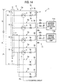
- Fig. 14 is a circuit diagram of a voltage equalizer
according to a ninth embodiment of the invention.
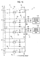
- Fig. 15 is a circuit diagram of a voltage equalizer
according to a tenth embodiment of the invention.
- Fig. 16 is a circuit diagram of a voltage equalizer
according to an eleventh embodiment of the invention.
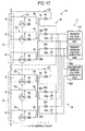
- Fig. 17 is a circuit diagram of a voltage equalizer
according to a twelfth embodiment of the invention.
-
DESCRIPTION OF THE PREFERRED EMBODIMENT
-
Voltage equalizers embodying the invention will now
be described by reference to the drawings.
<FIRST EMBODIMENT>
-
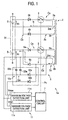
Firstly, referring to Fig. 1, a voltage equalizer 1a
according to a first embodiment of the inventionwill be described,
the first embodiment constituting a base mode for carrying
out the invention.
-
In the figure, reference numeral 31 denotes a battery,
in particular, a battery that is installed in electric vehicles
run by motors and hybrid vehicles run by using engines in
combination with motors. This battery 31 is such as to be
made up of a plurality of battery elements B ... which are connected
in series, and various types of battery elements including
ion batteries such as lithium ion batteries and electric double
layer capacitors can be used for the battery elements B... .
In addition, each battery element B may be made up of a single
cell or a plurality of cells, which are connected in series,
in parallel, or in combination thereof. Then, a voltage
equalizer 1a for equalizing terminal voltages Vo... of the
respective battery elements B... is connected to the battery
31.
-
The voltage equalizer 1a includes a transformer 2 having
an iron core. The transformer 2 has a plurality of basic windings
2o... which are provided in such a manner as to correspond,
respectively, to the battery elements B... . In addition,
each basic winding 2o has a primary winding 2a and a secondary
winding 2b which are separated by a center tap (an intermediate
tap) 2oc, and the center tap 2oc is connected to a negative
pole side of the corresponding battery element B. In this
case, numbers of turns of the respective basic windings 2o...
are set to be the same. The primary windings 2a... and the
secondary windings 2b... in the first embodiment have the same
number of turns. Note that the center tap 2oc functions a
winding termination terminal of the secondary winding 2b as
well as a winding initiation terminal of the primary winding
2a. On the other hand, a series circuit of a switching element
3 and a primary diode (a one-way conductor element) 5a is connected
between a winding termination terminal of the primary winding
2a and a positive pole side of the corresponding battery element
B, and a winding initiation terminal of the secondary winding
2b is connected to the positive pole side of the corresponding
battery element B via a secondary diode (a one-way conductor
element) 5b, whereby a plurality of primary series circuits
Ca... are configured in each of which current is carried from
the battery element B via the corresponding primary diode 5a
to the primary winding 2a (the basic winding 2o), when the
switching element 3 is switched on, and a plurality of secondary
series circuit Cb... are configured in each of which current
is carried from the secondary winding 2b (the basic winding
2o) via the secondary diode 5b to the battery element B, when
the switching element 3 is switched off. Consequently, the
primary windings 2a... are used for the primary series circuits
Ca... , and the secondary windings 2b ... are used for the secondary
series circuits Cb... . In addition, a semiconductor switch
such as an FET is used for the switching elements 3... . Thus,
an equalization processing circuit 6 is configured.
-
On the other hand, reference numeral 7 denotes a control
circuit. The control circuit 7 outputs a pulse control signal
Ps which is oscillated from a pulse oscillator installed therein
and whose frequency is in the order of a hundred kHz, and the
respective switching elements 3... are ON/OFF controlled in
a synchronized fashion by this pulse control signal Ps.
-
Furthermore, a voltage detection circuit 11 is connected
to the equalization processing circuit 6 for detecting a maximum
terminal voltage Vmax and a minimum terminal voltage Vmin in
the respective (all) battery elements B... . In this case,
the voltage detection circuit 11 includes a maximum voltage
detection unit 11m and a minimum voltage detection unit 11s,
and a winding termination terminal of the primary winding 2a
of any basic winding 2o is connected to one of input ports
of the maximum voltage detection unit 11m via a diode 32, and
a center tap 2oc of the relevant basic winding 2oc is connected
to the other input port of the maximum voltage detection unit
11m. In addition, a winding termination terminal of the
secondary winding 2b of the basic winding 2o is connected to
one of input ports of the minimum voltage detection unit 11s
via a diode 32b, and a center tap 2oc of the basic winding
2o is connected to the other input port of the minimum voltage
detection unit 11s. Then, a voltage holding capacitor 33a
is connected between an output side of the diode 32a and the
center tap 2oc, and a voltage holding capacitor 33b is connected
between an output side of the diode 32b and the center tap
2oc. The diode 32a and the voltage holding capacitor 33a
constitute a maximum voltage holding circuit 12m for holding
(storing) a maximum terminal voltage Vmax, and the diode 32b
and the voltage holding capacitor 33b constitute a minimum
voltage holding circuit 12s for holding (storing) a minimum
terminal voltage Vmin. By providing the maximum voltage holding
circuit 12m and the minimum voltage holding circuit 12s, a
maximum terminal voltage Vmax that is generated when the
respective switching elements 3... are switched on and a minimum
terminal voltage Vmin that is generated when the respective
switching element 3... are switched off can be detected without
being affected by ON/OFF timings of the respective switching
elements 3... , therebymaking it possible to attempt to simplify
a detection processing system.
-
Next, referring Fig. 1 and Figs. 3 to 6, the operation
of the voltage equalizer 1a according to the first embodiment
will be described in accordance with a flowchart shown in Fig.
2.
-
Firstly, when the voltage equalizer 1a is activated,
pulse signals Ps are given to the respective switching elements
3... by the control circuit 7, and the switching elements 3...
are ON/OFF controlled while being synchronized with the pulse
control signals Ps so given to them. An ON/OFF condition (pulse
control signal Ps) of the switching elements 3... is shown
in Fig. 5A.
-
Now, assume that the respective switching elements
3... are switched on (step S1). An equivalent circuit Ua of
the voltage equalizer 1a when the respective switching elements
3... are switched on is shown in Fig. 3. As this occurs, the
plurality of primary series circuits Ca... are configured in
each of which current is carried from the battery element B
to the primary winding 2a via the corresponding diode 5a, and
the respective primary circuits Ca... so configuredare connected
in parallel with each other. As a result, a storage current
Is flows from the battery element B in all of the battery elements
B... which has a largest terminal voltage Vo or the battery
element B having a maximum terminal voltage Vomax to the primary
winding 2a in association with storage of energy into the
transformer 2, and since a maximum terminal voltage Vmax is
generated in all of the primary windings 2a... , storage currents
Is... do not flow from the battery elements B... whose terminal
voltage Vo is smaller than the maximum terminal voltage Vmax.
Note that there may occur a case where only one battery element
B generates the maximum terminal voltage Vomax, or a case where
two or more battery elements B... generate the maximum terminal
voltage Vomax. A path along which the storage current Is flows
is shown by an arrow followed by a chain line in Fig. 1. Thus,
since energy is stored in the transformer 2 through the flow
of the storage current Is only from the battery element B having
the maximum terminal voltage Vomax, an equalization process
is performed to reduce the maximum terminal voltage Vomax of
the relevant battery element B (step S2).
-
In addition, as shown in Fig. 3, the maximum terminal
voltage Vmax that is generated at both terminals (a winding
initiation terminal and a winding termination terminal) of
the primary winding 2a is held (stored) by the maximum voltage
holding circuit 12m. Namely, the maximum terminal voltage
Vmax is supplied to the voltage holding capacitor 33a via the
diode 32a and is held as the terminal voltage of the voltage
holding capacitor 33a (step S3). Incidentally, as shown in
Fig. 5B, the storage current Is increases gradually from the
point in time when the respective switching elements 3... are
switched on. Due to this, the terminal voltage Va of the primary
winding 2a and the maximum terminal voltage Vmax which is an
output from the diode 32a become as shown in Fig. 5C, and although
a normal voltage corresponding to the maximum terminal voltage
Vomax of the battery element B is generated immediately after
the respective switching elements 3 ... are switched on, a portion
corresponding to a voltage drop in the primary diode 5a increases
as the storage current Is increases, whereby the terminal voltage
Va of the primary winding 2a and the maximum terminal voltage
Vmax which is the output from the diode 32a also decrease gradually.
Consequently, the maximum terminal voltage Vmax that is held
by the maximum voltage holding circuit 12m includes an error
corresponding to the voltage drop. Note that since little
current flows to the diode 32a, a voltage drop by the diode
32a can be ignored.
-
Next, assume that the respective switching elements
3... are switched off (step S4). An equivalent circuit Ub
of the voltage equalizer 1a when the respective switching
elements 3... are switched off is shown in Fig. 4. As this
occurs, the plurality of secondary series circuits Cb... are
configured in each of which current is carried from the secondary
winding 2b to the battery element B via the secondary diode
5b, and the secondary series circuits Cb... so configured are
connected in parallel with each other. As a result, an emission
current Ir flows from the secondary winding 2b to the battery
element B in all of the battery elements B... which has a smallest
terminal voltage Vo or the battery element B having a minimum
terminal voltage Vomin in association with emission of energy
from the transform 2, and since the minimum terminal voltage
Vomin is generated in all of the secondary windings 2b... ,
emission currents Ir do not flow to the battery elements B...
whose terminal voltage Vo is larger than the minimum terminal
voltage Vomin. Note that there may occur a case where only
one battery element B generates the minimum terminal voltage
Vomin, or a case where two or more battery elements B... generate
the minimum terminal voltage Vomin. A path along which the
emission current Ir flows is shown by an arrow followed by
a chain line in Fig. 1. Thus, since the charging of the battery
element B is implemented through the flow of the emission current
Ir only to the battery element B having the minimum terminal
voltage Vomin, an equalization process is performed to increase
the minimum terminal voltage Vomin of the relevant battery
element B (step S5).
-
In addition, as shown in Fig. 4, the minimum terminal
voltage Vimin that is generated at both terminals (a winding
initiation terminal and a winding termination terminal) of
the secondary winding 2b is held (stored) by the minimum voltage
holding circuit 12s. Namely, the minimum terminal voltage
Vmin is supplied to the voltage holding capacitor 33b via the
diode 32b and is held as the terminal voltage of the voltage
holding capacitor 33b (step S6). Incidentally, as shown in
Fig. 5B, the emission current Ir decreases gradually from the
point in time when the respective switching elements 3... are
switched off. Due to this, the terminal voltage Vb of the
secondary winding 2b and the minimum terminal voltage Vmin
which is an output from the diode 32b become as shown in Fig.
5D, and although a minimum terminal voltage Vmin to which a
voltage drop in the secondary diode 5b is added to a largest
extent is generated immediately after the respective switching
elements 3... are switched off, a portion corresponding to
the voltage drop decreases as the emission current Ir decreases,
whereby the terminal voltage Vb of the secondary winding 2b
and the minimum terminal voltage Vmin which is the output from
the diode 32b also decrease gradually. Then, a minimum terminal
voltage Vmin resulting immediately before the emission currents
Ir... generated in association with the emission of energy
from the transformer 2 become zero after the switching elements
3... are switched off becomes a normal voltage corresponding
to the minimum terminal voltage Vomin of the battery element
B. Consequently, the minimum terminal voltage Vmin held by
the minimum voltage holding circuit 12s includes an error
corresponding to the voltage drop. Note that since little
current flows to the diode 32b, a voltage drop by the diode
32b can be ignored.
-
Thus, the voltage equalization process is implemented
on the respective battery elements B... by repeating the ON/OFF
operations of the switching elements 3... , and in the end,
the terminal voltages Vo of all the battery elements B... are
equalized. Thus, in the equalization processing circuit 6,
since, when the respective switching elements 3... are switched
on, the storage currents Is... generated in association with
the storage of energy into the transformer 2 are caused to
flow from the battery elements B... having the maximum terminal
voltage Vomax to the basic windings 2o... , whereas, when the
respective switching elements 3... are switched off, the emission
currents Ir... generated in association with the emission of
energy from the transformer 2 are caused to flow from the basic
windings 2o... to the battery elements B... having the minimum
terminal voltage Vomin, the equalization process can be
implemented both when energy is stored into the transformer
2 and when energy is emitted from the transformer 2, whereby
the equalizing ability and equalizing efficiency can be enhanced
remarkably. In addition, even in the event that the terminal
voltages Vo... of the battery elements B... vary largely, since
the emission currents Ir... (the storage currents Is...) flow
through the secondary series circuits Cb... (the primary series
circuits Ca...) individually, the generation of an adverse
effect that excessive emission currents Ir... (storage currents
Is...) flow when the equalizing process is being carried out
can be prevented.
-
On the other hand, in the voltage detection circuit
11, maximum terminal voltage Vmax and minimum terminal voltage
Vmin detection processes are carried out when predetermined
sampling times are reached (steps S7, S8). In this case, since
the maximum terminal voltage Vmax is held in the maximum voltage
holding circuit 12m (the voltage holding capacitor 33a), the
maximum terminal voltage Vmax can be detected only by reading
the terminal voltage of the voltage holding capacitor 33a by
the maximum voltage detection unit 11m. Then, the maximum
terminal voltage Vmax so detected is sent to the control circuit
7 as a datum to be stored in a memory of the control circuit
7 at least temporarily. Similarly, since the minimum terminal
voltage Vmin is held in the minimum voltage holding circuit
12s (the voltage holding capacitor 33b), the minimum terminal
voltage Vmin can be detected only by reading the terminal voltage
of the voltage holding capacitor 33b by the minimum voltage
detection unit 11s. Then, the minimum terminal voltage Vmin
so detected is sent to the control circuit 7 to be stored in
the memory of the control circuit 7 at least temporarily.
-
Thus, according to the voltage detection circuit 11,
the maximum terminal voltage Vmax and the minimum terminal
voltage Vmin can easily be detected, and since the voltage
detection circuit 11 also functions as a substantial part of
the voltage equalizer 1a, the configuration of the voltage
equalizer 1a can be attempted to be simplified. Moreover,
since the necessity of a conventional detection circuit for
independently detecting each of the terminal voltages Vo...
of the respective battery elements B... can be obviated, when
thinking of the entirety of the system, the production cost
can be reduced, the energy loss can be reduced, and the size
can be made compact. Since a main obj ect of the voltage detection
circuit 11 is to detect the battery elements B... whose terminal
voltages Vo... deviate from the normal range to thereby become
extraordinarily low or high, the object can be sufficiently
met when only the maximum terminal voltage Vmax and the minimum
terminal voltage Vmin can be detected, and therefore, there
is no need to detect even normal terminal voltages Vo...
Consequently, the original object can be attained to a sufficient
extent in the event that the voltage detection circuit 11
according to the first embodiment is used which detects only
the maximum terminal voltage Vmax and the minimum terminal
voltage Vmin.
-
In addition, since the maximum voltage holding circuit
12m and the minimum voltage holding circuit 12s are provided
in the voltage detection circuit 11, the maximum terminal voltage
Vmax that is generated when the respective switching elements
3... are switched on and the minimum terminal voltage Vmin
that is generated when the respective switching elements 3...
are switched off can be detected without being affected by
ON/OFF timings of the respective switching elements 3... .
In this case, while there is entrained a disadvantage that
the voltage by the respective diodes 5a, 5b, 32a, 32b are contained
as errors, there is provided an advantage that the detection
processing system can be attempted to be simplified.
-
Fig. 6 shows experimental data on maximum terminal
voltages Vmax and minimum terminal voltages Vmin detected by
the voltage detection circuit 11 according to the first
embodiment. In experiments, a battery 31 was used in which
eight battery elements B... are connected in series. In Fig.
6, Vo[V] represents measured data which resulted from direct
measuring of terminal voltages of the respective battery elements
B... . In addition, an experimental result No. 1 shows a sample
which includes six battery elements 2 to 7 which have average
terminal voltages, one battery element 1 whose terminal voltage
is relatively low and one battery element 8 whose terminal
voltage is relatively high, and an experimental result No.
2 shows a sample which is a combination of battery elements
1 to 4 whose terminal voltages are relatively low and battery
elements 5 to 8 whose terminal voltages are relatively high.
-
In the experimental result No. 1, a minimum terminal
voltage Vmin and a maximum terminal voltage Vmax detected by
the voltage detection circuit 11 were 2.034[V] and 3.970[V],
respectively. Consequently, the terminal voltage of the
battery element 1 which constitutes a minimum voltage was
2.003[V], and an error therefrom was 0.031[V] (1.55[%]). In
addition, the terminal voltage of the battery element 8 which
constitutes a maximum voltage was 4.032[V], and an error
therefrom was -0.062[V] (-1.54[%]). Furthermore, in the
experimental result No. 2, a minimum terminal voltage Vmin
and a maximum terminal voltage Vmax detected by the voltage
detection circuit 11 were 2.046[V] and 3.943[V], respectively.
Consequently, the terminal voltage of the battery element
4 which constitutes a minimum voltage was 2. 062[V], and an
error therefrom was -0.016[V] (-0.78[%]). In addition, the
terminal voltages of the battery elements 7, 8 which constitute
a maximum voltage were 3.946[V], and an error therefrom was
-0.003[V] (-0.08[%]). Thus, by using the voltage detection
circuit 11, a highly accurate detection can be attained with
respect to the maximum terminal voltage Vmax and the minimum
terminal voltage Vmin.
-
On the other hand, the data as to the maximum terminal
voltage Vmax and the minimum terminal voltage Vmin which are
temporarily stored in the control circuit 7 are used to set
a control condition for the switching elements 3... . Firstly,
in the control circuit 7, a difference between the maximum
terminal voltage Vmax and the minimum terminal voltage Vmin
(a differential voltage Ve) is obtained through an operation
process of Vmax-Vmin=Ve (step S9). Then, if the differential
voltage Ve so obtained is equal to or smaller than a set value
Es which was set in advance, the ON/OFF control of the switching
elements 3... is stopped, so that the switching elements 3...
are in the OFF state (steps S10, S11). As this occurs, since
a small differential voltage Ve means that the terminal voltages
Vo... of the respective battery elements B... vary a little,
needing no equalization process, a wasteful energy consumption
can be avoided by stopping the equalization process. On the
contrary, when the differential voltage Ve exceeds the set
value Es, the terminal voltages Vo... of the respective battery
elements B... vary largely, needing an equalization process,
and consequently, the ON/OFF control of the switching elements
3... is made to continue as it is (step S10).
-
In addition, when the differential voltage Ve exceeds
the set value Es, a switching frequency fs for ON/OFF controlling
the switching elements 3... is caused to change in accordance
with the magnitude of the differential voltage Ve (steps S10,
S11). Namely, when the differential voltage Ve is large, a
control condition changing process for setting the switching
frequency fs low is performed, whereas, when the differential
voltage Ve is small, a control condition changing process for
setting the switching frequency fs high is performed. Thus,
when the differential voltage Ve is small, the amount of energy
stored in and emitted from the transformer 2 is reduced so
as to reduce a wasteful loss by reducing the time when the
switching elements 3... are ON, whereas, when the differential
voltage Ve is large, the capability of the equalization process
can be increased by increasing the time when the switching
elements 3... are ON.
-
Next, voltage equalizers 1b to 1m according to modified
embodiments (second to twelfth embodiments) of the invention
will be described by reference to Figs. 7 to 17.
-
Firstly, referring to Figs. 7 to 13, voltage equalizers
1b to 1h according second to eighth embodiments of the invention
will be described.
<SECOND EMBODIMENT>
-
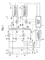
Initially, referring to Fig. 7, a voltage equalizer
1b according to a second embodiment will be described. With
a voltage detection circuit 11 being modified, this voltage
equalizer 1b differs from the voltage equalizer 1b of the first
embodiment in that a maximum terminal voltage Vmax and a minimum
terminal voltage Vmin are detected by a detection winding 2d
which is provided separately in the transformer 2, that a
detection timing is set so that a maximum terminal voltage
Vmax and a minimum terminal voltage Vmin can be detected
accurately, and that a pulse control signal Ps, which performs
a self-oscillation and changes its frequency in accordance
with the magnitudes of storage currents Is... and emission
currents Ir... , is used when ON/OFF controlling the switching
elements 3....
-
Consequently, the voltage equalizer 1b has the detection
winding 2d which is provided separately in the transformer
2 and which includes a primary detection winding 2da and a
secondary detection winding 2db. Since the primary detection
winding 2da is used to detect a maximum terminal voltage Vmax,
a winding termination terminal thereof is connected to one
of input ports of a maximum voltage detection unit 11m via
a diode 32a, and a winding initiation terminal thereof is
connected to the other input port of the maximum voltage detection
unit 11m via a switching element 51a. In addition, since the
other secondary detection winding 2db is used to detect a minimum
terminal voltage Vmin, a winding initiation terminal thereof
is connected to one of input ports of a minimum voltage detection
unit 11s via a diode 32b, and a winding termination terminal
thereof is connected to the other input port of the minimum
voltage detection unit 11s via a switching element 51b. In
this case, in the event that the number of turns of the primary
detection winding 2da is made to coincide with the number of
turns of a primary winding 2a of a basic winding 2o, whereas
the number of turns of the secondary detection winding 2db
is made to coincide with the number of turns of a secondary
winding 2b of the basic winding 2o, as done by the voltage
detection circuit 11 provided in the voltage equalizer 1a of
the first embodiment, a maximum terminal voltage Vmax and a
minimum terminal voltage vmin can be detected. By providing
the detection winding 2d, there are provided advantages that
an electrical insulation relative to a voltage equalization
processing circuit 6 can be attempted and that the detection
voltage can be increased or decreased as required.
-
In addition, a current detection unit 55 is provided
in the equalizationprocessing circuit 6. The current detection
unit 55 includes a detection transformer 57 having current
detection windings 57f... which functions as a current
transformer (CT) and a detection processing unit 58. The
respective current detection windings 57f... connect in series
between positive pole sides of respective battery elements
B... and respective diodes 5a and 5b so as to detect the magnitude
of emission currents Ir... which flow into the battery elements
B... or storage currents Is... which flow out of the battery
elements B... , and an output winding 57s of the detection
transformer 57 is connected to an input side of the detection
processing unit 58, an output side of the detection processing
unit 58 connecting to a control circuit 7. Note that additionally,
like reference numerals are imparted to like portions in Fig.
7 to those shown in Fig. 1 so as not only to make clear the
configuration shown in Fig. 7 but also to omit a detailed
description thereof.
-
The operation inherent in the voltage equalizer 1b
according to the second embodiment will be described as below.
Firstly, the ON/OFF control of the switching elements 3...
is not implemented by a pulse control signal Ps whose frequency
is stationary but by a pulse control signal Ps whose frequency
is variable in accordance with the magnitude of storage currents
Is... and emission currents Ir... . This pulse signal Ps is
generated as follows. Now, assume that the switching elements
3... are in the OFF state. In this case, emission currents
Ir... are detected by the current detection unit 55. Since
the emission currents Ir decrease gradually as shown in Fig.
5B, the control circuit 7 monitors the magnitude of emission
currents Ir... which are detected and starts the ON control
of the switching elements 3... at a timing when a predetermined
time Tr, which is set in advance, has elapsed since the emission
currents Ir... became zero. On the other hand, after the
switching elements 3... have been switched on, storage currents
Is... flow, and since the storage currents Is... so flowing
are detected by the current detection unit 55 and gradually
decrease as shown in Fig. 5B, the control circuit 7 monitors
the magnitude of the storage currents Is... so detected and
starts the OFF control of the switching elements 3... at a
timing when the storage currents Is... have reached a
predetermined value Ism.
-
Thereby, the control circuit 7 starts self-oscillation,
and therefore, a separate oscillator which oscillates a
stationary switching frequency (ON/OFF frequency) fs is no
more required. In addition, since the frequency is variable,
an excessive current can be prevented and stable storage currents
Is ... can be caused to flow at all times. In addition, no-current
time period can be eliminated, so that a voltage equalizing
process can be performed efficiently. Due to this, it is
desirable to set the length of the predetermined time Tr and
the magnitude of the predetermined value Ism so as to obtain
those effects.
-
Furthermore, although the storage currents Is... flow
to the primary windings 2a... , when the respective switching
elements 3... are switched on, since the storage currents Is...
become least immediately after the switching elements 3...
have been switched on, a voltage drop by the primary diodes
5a... can be ignored. Then, the control circuit 7 starts the
ON control of the switch element 51a in the voltage detection
circuit 11 at a timing when a predetermined time Td, which
is set in advance, has elapsed since the switching elements
3... were switched on and performs a process in which a maximum
terminal voltage Vmax is detected by the maximum voltage
detection unit 11m. Namely, the switching element 51a is ON
controlled only when the maximum terminal voltage Vmax is
detected, whereby since an error that would be generated by
the voltage drops by the primary diodes 5a... can be ignored
and the maximum terminal voltage Vmax can be detected at a
constant detection timing at all times, a maximum terminal
voltage Vmax which is free from variation and is accurate can
be detected.
-
On the other hand, although emission currents Ir...
flow to the secondary windings 2b... , when the respective
switching elements 3... are switched off, since the emission
currents Ir... become least immediately before they become
zero, a voltage drop by the secondary diodes 5b... can be ignored.
Then, the control circuit 7 monitors the magnitude of the
emission currents Ir... after the switching elements 3... have
been switched off and starts the ON control of the switching
element 51b in the voltage detection circuit 11 at a timing
(a point ts in Fig. 5B) when a predetermined threshold Irs
has been reached, a process being carried out in which a maximum
terminal voltage Vmin is detected by the minimum voltage
detection unit 11s. Namely, the switching element 51b is ON
controlled only when the maximum terminal voltage Vmin is
detected, whereby since not only can an error by the voltage
drop by the secondary diodes 5b... be ignored, but also the
minimum terminal voltage Vmin can be detected at a constant
detection timing at all times, a minimum terminal voltage Vmin
which is free from variation and is accurate can be detected.
Note that the detection of maximum terminal voltage Vmax and
minimum terminal voltage Vmin at the set detection timings
can equally be implemented even when a pulse oscillator is
used which oscillates a stationary switching frequency (ON/OFF
frequency) fs.
-
In addition, the detection of a minimum terminal voltage
Vmin can also be carried out in the following manner. Namely,
the minimum voltage detection unit 11s obtains in advance through
an operation a predetermined time Ts that is spent the magnitude
of emission currents Ir... generated in association with the
emission of energy from the transformer 2 decreases to a
predetermined threshold Irs and can detect a minimum terminal
voltage Vmin at a timing when the predetermined time Ts has
elapsed since the switching elements 3... were switched off.
This obviates the necessity of detection of emission currents
Ir... , thereby making it possible to attempt to simplify the
detection processing system.
<THIRD EMBODIMENT>
-
Next, referring to Fig. 8, a voltage equalizer 1c
according to a third embodiment will be described. This voltage
equalizer 1c differs from the voltage equalizer 1a of the first
embodiment in that primary windings 2a... and secondary windings
2b... are made up of windings which are completely separated,
that a winding having a center tap is used for a separate winding
2d provided in a voltage detection circuit 11, and that a
correction circuit 13 is provided. In this case, the voltage
detection circuit 11 utilizes the separate detection winding
2d shown in Fig. 7, the maximum voltage holding circuit 12m
and the minimum voltage holding circuit 12s which are shown
in Fig. 1 are combined, and a correction circuit 13 is provided
for correcting a voltage detected from the terminal voltage
of the detection winding 2d. The correction circuit 13 is
such as to construct a closed circuit by connecting a diode
64, a resistor 65 and diodes 66 and 67 in series to a correction
winding 63. By this configuration, since a correction voltage
corresponding to a voltage drop by diodes 5a... is generated
at both ends of the diodes 66 and 67, this correction voltage
is added to a maximum terminal voltage Vmax which is detected
as an end-to-end voltage of a voltage holding capacitor 33a
so as to correct the maximum terminal voltage Vmax so detected,
thereby making it possible to obtain a maximum terminal voltage
Vmax which excludes an error due to the voltage drop by the
diodes 5a... . In addition, reference numeral 68 denotes a
capacitor, and reference numerals 61a, 61b denote, respectively,
resistors which are connected in parallel to the voltage holding
capacitors 33a, 33b. While the embodiment is described as
the maximum terminal voltage Vmax being corrected, a correction
circuit for correcting a minimum terminal voltage can equally
be provided. Alternatively, a similar correction to the
correction implemented by the correction circuit 13 may be
implemented using a digital processing function performed in
a voltage detection unit 11c. Note that both the maximum voltage
detection unit 11m and the minimum voltage detection unit 11s
are contained in the voltage detection unit 11c. In addition,
in Fig. 8, a path along which storage current Ir flows when
switching elements 3... are switched off is shown by an arrow
followed by a chain line, and a path along which emission current
Ir flows when the switching elements 3... are switched off
is shown by an arrow followed by a chain line. Since the basic
configuration of the voltage equalizer 1c becomes identical
with that of the voltage equalizer 1a of the first embodiment,
the basic operations of an equalization processing circuit
6 and a voltage detection circuit 11 in the voltage equalizer
1c become also identical with those of the voltage equalizer
1a of the first embodiment. Note that additionally, in Fig.
8, like reference numerals are imparted to like portions to
those in Figs. 1 and 7 so as not only tomake clear the configuration
in Fig. 8 but also to omit a detailed description thereof.
<FOURTH EMBODIMENT>
-
Next, referring to Fig. 9, a voltage equalizer 1d
according to a fourth embodiment will be described below.
This voltage equalizer 1d differs from the voltage equalizer
1a of the first embodiment in that basic windings 2o... are
made up of single windings and are used both for primary series
circuits Ca... in corresponding battery elements B... and
secondary series circuits Cb... in other battery elements B... ,
and that an auxiliary winding 2x is provided in a transformer
2, so that the auxiliary winding 2x so provided is used as
a secondary series circuit Cb in the battery element B in which
a secondary series circuit Cb is not configured depending on
the basic winding 2o. A secondary winding 2db in Fig. 9 is
intended to detect a minimum terminal voltage Vmin. By this
configuration, when switching elements 3... are switched on,
storage currents Is... flow along a path indicated by an arrow
followed by a chain line in Fig. 9, whereas, when the switching
elements 3... are switched off, emission currents Ir... flow
along paths indicated by arrows followed by chain lines in
Fig. 9. by using the voltage equalizer 1d configured as has
been described above, while the auxiliary winding 2x needs
to be added, there is provided an advantage that the basic
windings 2o... can be made up of the single winding of which
the number of turns is identical with that of the aforesaid
primary winding 2a (or the secondary winding 2b). Note that
additionally, in Fig. 9, like reference numerals are imparted
to like portions to those shown in Fig. 1 so as not only to
make clear the configuration shown in Fig. 9 but also to omit
a detailed description thereof.
<FIFTH EMBODIMENT>
-
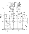
Next, referring to Fig. 10, a voltage equalizer 1e
according to a fifth embodiment of the inventionwill be described
below. This voltage equalizer 1e is a modification made to
the voltage equalizer 1d of the fourth embodiment and differs
from the voltage equalizer 1d in that locations where respective
components are connected are modified and that a detection
winding 2d is made up of a separate winding. Consequently,
the secondary winding 2db for detecting the minimum terminal
voltage Vmin shown in Fig. 9 can be eliminated, whereby, when
switching elements 3... are switched on, storage currents Is...
flow along a path indicated by an arrow followed by a chain
line in Fig. 10, whereas, when the switching elements 3...
are switched off, emission currents Ir... flow along paths
indicated by arrows followed by chain lines in Fig. 10. As
with the voltage equalizer 1d of the fourth embodiment, while
the voltage equalizer 1e requires one auxiliary winding 2x,
there can be provided an advantage that basic windings 2o...
can be made up of a single winding of which the number of turns
is identical with that of the aforesaid primary winding 2a
(of the secondary winding 2b). Note that additionally, in
Fig. 10, like reference numerals are imparted to like portions
to those shown in Figs. 8 and 9 so as not only to make clear
the configuration shown in Fig. 10 but also to omit a detailed
description thereof.
<SIXTH EMBODIMENT>
-
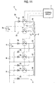
Next, referring to Fig. 11, a voltage equalizer 1f
according to a sixth embodiment will be described below. This
voltage equalizer 1f differs from the voltage equalizer 1d
according to the fourth embodiment in that an energy
replenishment circuit 22 and an energy discharge circuit 26
are provided. Namely, the voltage equalizer 1f includes the
energy replenishment circuit 22 which conf igures a closed circuit
by connecting in series a replenishment winding 2s provided
in a transformer 2 for replenishing energy, a battery unit
Bs for replenishing the replenishment winding 2s with energy
and a replenishment switching unit 21. In this case, assuming
that a maximum terminal voltage of battery elements B... is
Vomax, the number of turns of a basic winding 2o is No, a terminal
voltage of the battery unit Bs is Vs, and the number of turns
of the replenishment winding 2s is Ns, Vs and/or Ns is set
so as to meet a condition for (Vs/Ns) >(Vomax/No). In addition,
a control circuit 7 is provided for ON/OFF controlling switching
elements 3... and the replenishment switching unit 21 while
causing them to synchronize with each other or ON/OFF controlling
the replenishment switching unit 21 with all of the switching
elements 3... being OFF controlled. Note that while being
omitted from the figure, as a voltage detection circuit 11,
the voltage detection circuit 11 shown in Fig. 10 can be provided.
-
By this configuration, in the event that the switching
elements 3... and the replenishment switching unit 21 are
synchronized with each other so as to be ON/OFF controlled
(or the replenishment switching unit 21 is ON/OFF controlled
with all of the switching elements 3... being OFF controlled) ,
the energy replenishment circuit 22 remains a source from which
the maximum terminal voltage Vomax is generated at all times,
whereby storage current Is flows along a path indicated by
an arrow followed by a chain line. Thus, the battery unit
Bs can replenish the battery elements B... with energy, whereby
an excessive self-discharge in the battery elements B... can
be avoided.
-
Furthermore, the voltage equalizer 1f includes the
energy discharge circuit 26 which configures a closed circuit
by connecting in series a discharge winding 2r provided in
the transformer 2 for discharging energy, the battery unit
Bs which is charged with energy discharged from the discharge
winding 2r, a diode 62 and a discharge switching unit 25.
In this case, assuming that a minimum terminal voltage of the
battery elements B... is Vomin, the number of turns of the
basic winding 2o is No, the terminal voltage of the battery
unit Bs is Vs and the number of turns of the discharge winding
2r is Nr, Vs and/or Nr is set so as to meet a condition for
(Vs/Nr)<(Vomin/No). In addition, the control circuit 7 is
provided for ON/OFF controlling the switching elements 3...
and the discharge switching unit 25 while causing them to
synchronize with each other in a reversed state or ON/OFF
controlling the switching elements 3... with the discharge
switching unit 25 being ON controlled.
-
By this configuration, in the event that the switching
elements 3... and the discharge switching unit 25 are caused
to synchronize with each other in the reverse state so as to
be ON/OFF controlled (or the switching elements 3... are ON/OFF
controlled with the discharge switching unit 25 being ON
controlled), the energy discharge circuit 26 remains a source
from which the minimum terminal voltage Vomin is generated
at all times, whereby emission currents Ir... flow along a
path indicated by an arrow followed by a chain line. Thus,
the battery unit Bs can be charged with energy of the battery
elements B... , whereby an excessive charging of the battery
elements B... can be avoided. Note that additionally, in Fig.
11, like reference numerals are imparted to like portions to
those shown in Fig. 9 so as not only to make clear the configuration
shown in Fig. 11 but also to omit a detailed description thereof.
<SEVENTH EMBODIMENT>
-
Next, referring to Fig. 12, a voltage equalizer 1g
according to a seventh embodiment of the invention will be
describedbelow. In this voltage equalizer 1g, the equalization
processing circuit in the voltage equalizer 1d shown in Fig.
9 is configured as a single module M, and a plurality of battery
elements B... which correspond to a plurality of modules M...
are connected in parallel to each other. In addition, in the
seventh embodiment, a primary winding 2da and a secondary winding
2db which constitute a voltage detection circuit 11 are connected
in parallel to each other, and diodes 32a, 32b and voltage
holding capacitors 33a, 33b are connected to the modules M...
in such a manner as to be used equally by the modules M... .
By configuring the equalization processing circuit 6 as a
module, for example, even in the event that the size of a
transformer 2 is standardized, it is possible to deal with
an arbitrary number of different battery elements B... in a
proper fashion. Then, the voltage equalization process can
be implemented as when the module M is used singly, and the
voltage detection by the voltage detection circuit 11 can be
implemented. Note that additionally, in Fig. 12, like reference
numerals are imparted to like portions to those shown in Fig.
9 so as not only to make clear the configuration shown in Fig.
12 but also to omit a detailed description thereof.
-
Furthermore, the configuration of the equalization
processing circuit into a module as described above can equally
be implemented in the aforesaid voltage equalizers 1a, 1b,
1c, 1e, 1f. Consequently, in general, the equalization
processing circuit 6 can be configured as a single module which
has a transformer 2 having, in turn, a plurality of basic windings
2o... which correspond, respectively, to battery elements B... ,
a plurality of switching elements 3... which correspond,
respectively, to the battery elements B... , and a plurality
of sets of primary diodes 5a... and secondary diodes 5b to
thereby configure a plurality of primary series circuits Ca...
in which current is carried from the respective battery elements
B... via the corresponding primary diodes 5a... to the respective
basic windings 2o... when the switching elements 3... are
switched on, and a plurality of secondary series circuits Cb...
in which current is carried from the respective basic windings
2o... via the secondary diodes 5b... to the respective battery
elements B... when the switching elements 3... are switched
off.
<EIGHTH EMBODIMENT>
-
Next, referring to Fig. 13, a voltage equalizer 1h
according to an eighth embodiment of the invention will be
describedbelow. In this voltage equalizer 1h, the equalization
processing circuit 6 in the voltage equalizer 1f according
to the sixth embodiment shown in Fig. 11 is configured as a
single module, and a plurality of battery elements B... which
correspond, respectively, to a plurality of modules M... are
connected in series to each other. In this case, a common
single battery unit Bs can be utilized, and a secondary diode
5b in any module M can be connected to an adjacent following
module M. In addition, while a voltage detection circuit 11
is omitted from Fig. 13, a voltage detection circuit 11 can
be provided as in the case shown in Fig. 12. Furthermore,
even in the event that the equalization processing circuits
6 in the aforesaid voltage equalizers 1a, 1b, 1c, 1d, 1e are
used to be configured into such a module M, the module M so
configured can equally be applied. Thus, also in the voltage
equalizer 1h, as in the case with the voltage equalizer 1g,
it is possible to deal with an arbitrary number of different
battery elements B... in a proper fashion. Then, a voltage
equalization process can be implemented as when the module
M is used singly, and the voltage detection by the voltage
detection circuit 11 can be implemented. Note that additionally,
in Fig. 13, like reference numerals are imparted to like portions
to those shown in Fig. 11 so as not only to make clear the
configuration shown in Fig. 13 but also to omit a detailed
description thereof.
-
Next, referring to Figs. 14 to 17, voltage equalizers
1i to 1m according to ninth to twelfth embodiments of the invention
will be described below. In any of the voltage equalizers
1i to 1m according to the ninth to twelfth embodiments, as
a minimum voltage detection unit, a minimum voltage detection
unit 11sg (11sga, 11sgb) is provided for detecting a minimum
end-to-end voltage of end-to-end voltages of respective groups
G... of one or two or more groups which result when a plurality
of battery elements B... are so grouped.
-
Incidentally, as has been described before, various
types of battery elements including ionbatteries such as lithium
ion batteries and electric double layer capacitors exist for
use as the battery element B. In this case, in ion batteries,
in the event that the terminal voltage Vo decreases below the
normal voltage, an excessive discharge is called for, and this
constitutes a cause for the failure of a battery. In the case
of capacitors such as electric double layer capacitors, however,
even in the event that the terminal voltage Vo decreases below
the normal voltage, there is no case where a problem (abnormality)
is caused. Consequently, with capacitors such as electric
double layer capacitors, it is not necessary to know accurately
the minimum terminal voltages Vomin... of the individual battery
elements B... , but it is sufficient to obtain information
on whether or not there is occurring a failure, and there is
a case where the information itself is not actually needed.
-
Then, in the voltage equalizers 1i to 1m according
to the ninth to twelfth embodiments, as to the detection of
minimum terminal voltages Vomin... , aminimumend-to-endvoltage
Vxmin of end-to-end terminal voltages of respective groups
G... of one or two or more groups resulting when a plurality
of battery elements B... are so grouped is designed to be detected
by a minimum voltage detection unit 11sg. Due to this, basic
windings 2o ... are each made up of a plurality of primary windings
2a... which correspond, respectively, to battery elements B...
and one or two or more secondary windings 2b... which correspond,
respectively, to groups G... of one or two or more groups which
result when the plurality of battery elements B ... are so grouped.
While minimum terminal voltages of the individual battery
elementsB... cannotbeobtained, theminimumend-to-endvoltages
Vxmin... so obtained can be used to anticipate the existence
of battery elements B... in which something abnormal is being
caused and to control the charging and discharging of the whole
battery 31.
<NINTH EMBODIMENT>
-
Firstly, referring to Fig. 14, the voltage equalizer
1i according to the ninth embodiment of the invention will
be described below. In this voltage equalizer, as an example,
there are provided four primary windings 2a... and two secondary
windings 2b, which is a half of the primary windings 2a...
Namely, basic windings 2o... has four primary windings 2a...
which correspond, respectively, to four battery elements B... ,
which are grouped into two groups G... of two battery elements,
and two secondary windings 2b... which correspond, respectively,
to the groups G.... In the case of the voltage equalizer
1i according to the ninth embodiment, primary series circuits
Ca... function in a similar way to that in which those of the
voltage equalizer 1a according to the first embodiment do.
Namely, when respective switching elements 3... are switched
on, storage current Is flows along a path indicated by an arrow
followed by a chain line in Fig. 14 in association with storage
of energy into a transformer 2, whereas, when the switching
elements 3... are switched off, emission currents Ir... flow
along paths indicated by arrows followed by a chain line in
Fig. 14 in association with emission of energy in the transformer
2 from the secondary windings 2b.... As this occurs, since
the discharge current Ir which flows from one of the secondary
windings 2b is supplied to the two battery elements B... which
are connected in series thereto via a secondary diode 5b so
as to charge them, a minimum end-to-end voltage Vxmin of
end-to-end voltages of the respective groups G... which are
each made up of the two battery elements B... is detected at
a minimum voltage detection unit 11sg.
-
Consequently, as has been described above, while the
minimum terminal voltage of the individual battery elements
B... cannot be obtained, by determining Vxmin/2, it is possible
to anticipate the existence of the battery elements B... in
which something abnormal is being caused and to control the
charging and discharging of the whole battery 31. In addition,
it is possible to attempt to reduce the production costs of,
reduce the size of and increase the efficiency of the entire
system by simplifying the circuit configuration on the side
of the secondary windings 2b... . Note that in this example,
it is possible to obtain a minimum terminal voltage Vmin which
can be compared with the aforesaid maximum terminal voltage
Vmax by halving the minimum end-to-end voltage Vxmin. This
is true with the equalizers 1j to 1m according to the tenth
to twelfth embodiments, which will be described below. Note
that additionally, in Fig. 14, like reference numerals are
imparted to like portions to those described in Figs. 8 and
10 so as not only to make clear the configuration shown in
Fig. 14 but also to omit a detailed description thereof.
<TENTH EMBODIMENT>
-
Next, referring to Fig. 15, the voltage equalizer 1j
according to the tenth embodiment of the invention will be
described below. In this voltage equalizer 1j, as an example,
five primary windings 2a... are provided, and two of the five
are also used as secondary windings 2b... . In Fig. 15, the
two primary windings 2a... to which secondary diodes 5b...
are connected are also used as the secondary windings 2b... ,
and two battery elements B... constitute a group G. Also,
in the case of the voltage equalizer 1j according to the tenth
embodiment, primary series circuits Ca... function in a similar
way to that in which those of the voltage equalizer 1a according
to the first embodiment do. Namely, when respective switching
elements 3... are switched on, storage current Is flows along
a path indicated by an arrow followed by a chain line in Fig.
15 in association with storage of energy into a transformer
2, whereas, when the switching elements 3... are switched off,
emission currents Ir... flow along paths indicated by arrows
followed by a chain line in Fig. 15 in association with emission
of energy in the transformer 2 from the secondary windings
2b... . As this occurs, since the discharge current Ir which
flows from one of the secondary windings 2b (the primary windings
2a) is supplied to the two battery elements B... which are
connected in series thereto via the secondary diode 5b so as
to charge them, a minimum end-to-end voltage Vxmin of end-to-end
voltages of the respective groups G... which are each made
up of the two battery elements B... is detected at a minimum
voltage detection unit 11sg. Consequently, a similar advantage
to that obtained by the voltage equalizer 1i of the ninth
embodiment can be obtained, and in particular, since at least
part of the primary windings 2a... is also used as the secondary
windings 2b... , this arrangement can contribute to a further
simplification of the circuit configuration. Note that
additionally, in Fig. 15, like reference numerals are imparted
to like portions to those shown in Fig. 10 so as not only to
make clear the configuration shown in Fig. 15 but also to omit
a detailed description thereof.
<ELEVENTH EMBODIMENT>
-
Next, referring to Fig. 16, the voltage equalizer 1k
according to the eleventh embodiment of the invention will
be described below. In this voltage equalizer 1k, a single
secondary winding 2b is provided, while a plurality of primary
windings 2a... are provided. Due to this, basic windings 2o
have a plurality of primary windings 2a... which correspond,
respectively, to battery elements B... , and all of the battery
elements B... are grouped into a single group G. Also, in
the case of the voltage equalizer 1k according to the eleventh
embodiment, primary series circuits Ca... function in a similar
way to that in which those of the voltage equalizer 1a according
to the first embodiment do. Namely, when respective switching
elements 3... are switched on, storage current Is flows along
a path indicated by an arrow followed by a chain line in Fig.
16 in association with storage of energy into a transformer
2, whereas, when the switching elements 3... are switched off,
emission currents Ir... flow along paths indicated by arrows
followed by a chain line in Fig. 16 in association with emission
of energy in the transformer 2 from the secondary winding 2b... .
As this occurs, the emission current Ir which flows out of
the single secondary winding 2b is supplied to all of the battery
elements B... (the entirety of a battery 31) which are connected
in series thereto via a second diode 5b so as to charge the
battery elements. Consequently, a special mode is generated
here in which the entire voltage of the battery 31 is detected
at a minimum voltage detection unit 11sg. Note that a similar
advantage to that obtained by the voltage equalizer 1i of the
ninth embodiment can be obtained with the voltage equalizer
1k according to the eleventh embodiment. Also note that
additionally, in Fig. 16, like reference numerals are imparted
to like portions to those shown in Fig. 14 so as not only to
make clear the configuration shown in Fig. 16 but also to omit
a detailed description thereof.
<TWELFTH EMBODIMENT>
-
Next, referring to Fig. 17, the voltage equalizer 1m
according to the twelfth embodiment of the invention will be
described below. In this voltage equalizer 1m, the voltage
equalizer 1k according to the eleventh embodiment is configured
into a single module M, and a plurality of (two in the embodiment)
models M... are connected in series. Consequently, the function
(operation) of each of the modules M... becomes identical with
that of the voltage equalizer 1k according to the eleventh
embodiment. In this case, terminal voltages of battery elements
B... of all the modules M... are equalized in a similar way
to that in which the terminal voltages of the battery elements
are equalized by the voltage equalizer 1k in the eleventh
embodiment. In addition, a maximum voltage detection unit
11m, a minimum voltage detection unit 11sga and a secondary
minimum voltage detection unit 11sgb are connected as shown
in Fig. 17, whereby a maximum terminal voltage Vomax of the
respective battery elements B... in all the modules M... can
be detected in the maximum voltage detection unit 11m, the
end-to-end voltage of a battery 31 in one (upper one in the
figure) of the modules M can be detected by the primary minimum
voltage detection unit 11sga, and the end-to-end voltage of
all the modules M... which results from the addition of the
end-to-end voltage of the upper module M and the end-to-end
voltage of the lower module M can be detected by the secondary
minimum voltage detection unit 11sgb. Note that by subtracting
the detection result of the primary minimum voltage detection
unit 11sga from the detection result of the secondary minimum
voltage detection unit 11sgb, the end-to-end voltage of the
other module (the lower one in the figure). Note that
additionally, in Fig. 17, like reference numerals are imparted
to like portions to those shown in Fig. 16 so as not only to
make clear the configuration shown in Fig. 17 but also to omit
a detailed description thereof.
-
Thus, while the various types of embodiments have been
described in detail, the invention is not limited thereto,
and any modification, addition and deletion may be made to
those embodiments with respect to the configurations of detailed
portions, materials, amounts and numerical values without
departing from the spirit and scope of the invention. For
example, various types of components and circuits which have
the same function can be used for switching elements, diodes,
voltage detection circuits and voltage holding circuits. In
addition, while the battery elements are described as battery
elements for use for a battery that is installed in electric
vehicles which are run by motors or hybrid vehicles which are
run in combination of an engine and a motor/s, the application
of the invention is not limited thereto.