EP1544724A1 - New FIFO memory structure and operting procedure of such a memory - Google Patents
New FIFO memory structure and operting procedure of such a memory Download PDFInfo
- Publication number
- EP1544724A1 EP1544724A1 EP04029809A EP04029809A EP1544724A1 EP 1544724 A1 EP1544724 A1 EP 1544724A1 EP 04029809 A EP04029809 A EP 04029809A EP 04029809 A EP04029809 A EP 04029809A EP 1544724 A1 EP1544724 A1 EP 1544724A1
- Authority
- EP
- European Patent Office
- Prior art keywords
- memory
- fifo
- words
- bits
- word
- Prior art date
- Legal status (The legal status is an assumption and is not a legal conclusion. Google has not performed a legal analysis and makes no representation as to the accuracy of the status listed.)
- Granted
Links
Images

Classifications
-
- G—PHYSICS
- G11—INFORMATION STORAGE
- G11C—STATIC STORES
- G11C11/00—Digital stores characterised by the use of particular electric or magnetic storage elements; Storage elements therefor
- G11C11/21—Digital stores characterised by the use of particular electric or magnetic storage elements; Storage elements therefor using electric elements
- G11C11/34—Digital stores characterised by the use of particular electric or magnetic storage elements; Storage elements therefor using electric elements using semiconductor devices
- G11C11/40—Digital stores characterised by the use of particular electric or magnetic storage elements; Storage elements therefor using electric elements using semiconductor devices using transistors
- G11C11/41—Digital stores characterised by the use of particular electric or magnetic storage elements; Storage elements therefor using electric elements using semiconductor devices using transistors forming static cells with positive feedback, i.e. cells not needing refreshing or charge regeneration, e.g. bistable multivibrator or Schmitt trigger
- G11C11/413—Auxiliary circuits, e.g. for addressing, decoding, driving, writing, sensing, timing or power reduction
- G11C11/417—Auxiliary circuits, e.g. for addressing, decoding, driving, writing, sensing, timing or power reduction for memory cells of the field-effect type
- G11C11/419—Read-write [R-W] circuits
-
- G—PHYSICS
- G06—COMPUTING; CALCULATING OR COUNTING
- G06F—ELECTRIC DIGITAL DATA PROCESSING
- G06F5/00—Methods or arrangements for data conversion without changing the order or content of the data handled
- G06F5/06—Methods or arrangements for data conversion without changing the order or content of the data handled for changing the speed of data flow, i.e. speed regularising or timing, e.g. delay lines, FIFO buffers; over- or underrun control therefor
- G06F5/10—Methods or arrangements for data conversion without changing the order or content of the data handled for changing the speed of data flow, i.e. speed regularising or timing, e.g. delay lines, FIFO buffers; over- or underrun control therefor having a sequence of storage locations each being individually accessible for both enqueue and dequeue operations, e.g. using random access memory
Definitions
- the invention relates to a first-of-a-kind memory, first out ", more commonly called FIFO memory (First In First Out).
- the FIFOs comprise essentially a basic memory (eg RAM type) of the size of the FIFO memory and including its circuits read / write, and logic circuits to handle the content of the FIFO, so that the words are read in the same order that they have been memorized (principle of the FIFO memory).
- the known FIFO memories are in general small (8 to 16 words of 8 bits).
- FIFO memories are currently built on the basis of a double basic memory port, including a read port and a port in writing, at the input and at the output of the FIFO memory.
- a example of such a memory is described in the document US 6,144,608.
- the main disadvantage of these memories is their size. The presence of the two ports is consequence that the silicon surface needed for the making a FIFO is about twice as much important that the silicon surface needed for the realization of a conventional memory of the same capacity (same number of words).
- memory points are in practice bigger and logic circuits, necessary to manage the contents of the FIFO memory and the presence of the two ports of the base memory, are more complex and therefore also bigger than those of a classical memory of the same capacity.
- Another disadvantage of these FIFO memories is their timing frequency (equal to the word flow at the input or output of the FIFO), which is limited in practice by the frequency of dual base port memory timing used to achieve them.
- FIFO memories are made on the basis of a simple port basic memory but used with a frequency twice as much as the frequency of the FIFO memory. The readings in the FIFO are thus performed during the even cycles of a clock signal setting the FIFO, while the writes in the FIFO are performed during the odd cycles of the signal clock.
- the main disadvantage of these FIFOs is that it must use a particularly fast basic memory (important frequency) to obtain a FIFO memory having a reasonable speed, since the frequency of the FIFO is halved compared to the frequency of the basic memory.
- the fast memories are in general expensive, because difficult to achieve, and also big consumers of energy.
- the subject of the invention is a new structure of FIFO memory does not have the disadvantages of FIFOs known.
- the subject of the invention is a FIFO memory of frequency f and size M words of n bits, to memorize successively words of n bits received in series on a input (DIN) and provide in series on an output (QOUT) the said words in the order in which they were stored.
- FIFO memory includes basic memory (110, 220) of frequency f / 2, able to memorize simultaneously two words of n bits successively received on the input (DIN) of the FIFO memory.
- FIFO memory also includes a memory circuit (130) for memorize either a n-bit word received on the input (DIN) the FIFO memory is simultaneously two words of n bits produced by the basic memory (110, 220) and for produce on the output OUT of the FIFO one of the words that said storage circuit (130) stores.
- a memory circuit (130) for memorize either a n-bit word received on the input (DIN) the FIFO memory is simultaneously two words of n bits produced by the basic memory (110, 220) and for produce on the output OUT of the FIFO one of the words that said storage circuit (130) stores.
- a FIFO memory of frequency f uses a basic memory Frequency f / 2, easier to perform and less expensive that a memory of the same size but frequency f.
- the basic memory used is a simple port memory as will be seen better in examples, which further limits its size.
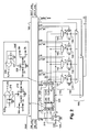
- FIG. memory is of size M * n (M words of n bits) and has a frequency f.
- the memory 100 includes a DIN input of n-bit data and QOUT output of n-bit data.
- the memory also includes two information outputs D_DRDY, Q_SRDY, two D_SRDY command entries, Q_DRDY and a RESET initialization input.
- the signal D_SRDY indicates to the memory that a datum is present at the DIN input to be stored.
- the signal Q_DRDY indicates to the memory that a data must be presented (read) on the Q output.
- the D_DRDY signal indicates that the memory is not full (and therefore a given can be input) and the signal Q_SRDY indicates that the memory is not empty (and therefore a datum can be read on the output Q).
- the RESET signal is used to initialize the memory, that is to say to erase its content, to activate the D_DRDY signal (memory not full) and disable the signal Q_SRDY (empty memory).
- the overall operation of the memory 100 is the next.
- D_SRDY and D_DRDY signals are active (in other words, n-bit data is present on the DIN input and the memory is not full), so the data is stored in the FIFO.
- the signals Q_DRDY and Q_SRDY are active (in other words, a n-bit data is expected on the QOUT output and the memory is not full)
- the data is presented on the Q output.
- the data is read on the QOUT output in the same order they were entered on the DIN input (principle of a FIFO memory.
- the memory 100 includes a RAM 110, a register 120 of n bits, a storage circuit 130 comprising four registers 131, 132, 133, 134 of n bits, a circuit selecting 140 comprising four multiplexers 141, 142, 143 and 144, a multiplexer 150 and a circuit logic 160.
- the memory 100 is clocked by a signal CLK clock of frequency f, which in particular register 120 and the circuit 130.
- the basic memory 110 is a RAM memory, for example of the SRAM type, with a single parallel port of 2 * n bits, comprising a data input and a data output of 2 * n bits.
- the memory 110 receives a signal from validation (CSN), a WEN command signal indicating whether write (WEN active) or read (WEN inactive) should be performed when the CSN signal is active and a ADD signal indicating the address at which two words of data must be written or read as appropriate.
- the memory 110 has a capacity of (M-3) / 2 words of 2 * n bits and has a frequency equal to f / 2, that is, it can memorize or provide a word of 2 * n bits (or two words of n bits in parallel) every two cycles of the CLK signal.
- the register 120 is an n-bit register, comprising a parallel D input of n-bit data connected to the DIN input of FIFO 100 and connected also to the n EH most significant bits of the input of the memory 110, a parallel Q output of n bits connected to the n least significant bits EL of the memory input 110.
- the register 120 receives a signal of RG_D validation and an active edge of the clock signal CLK, it copies on its output Q the data present on D.
- the registers 131, 132, 133, 134 are identical to the register 120.
- register 131 When the register 131, respectively, 132, 133, 134, receives an active edge of clock signal CLK and a validation signal EN0, respectively EN1, EN2, EN3, register 131, respectively 132, 133, 134 copy on its output Q la data present on his entry D.
- Data entry D of register 131, respectively 132, 133, 134, is connected to an output of the multiplexer 140, respectively 141, 142, 143.
- Each multiplexer 140, 141, 142, 143 has three parallel inputs of n bits, connected respectively to the n most significant bits SH of the output of the memory 110, to the low-order bits SL of the output of the memory 110 and the output of n bits 120.
- Each multiplexer provides on its output a data it receives on one or the other of its inputs according to a selection signal SEL_IN0, SEL_IN1, SEL_IN2, SEL_IN3.
- the multiplexer 150 includes meanwhile five parallel inputs of n bits, each connected to the output of a register 120, 131, 132, 133 or 134, and a parallel output of n bits forming the output QOUT of the FIFO memory.
- the multiplexer 150 provides on his output a data he receives on one of his five inputs according to the selection signals R_J and LEVEL_EQUAL_1.
- the logic circuit 160, the memory 110 and the registers 120, 131, 132, 133, 134 are synchronized and clocked by a clock signal CLK (the circuit clock is not shown for the sake of clarity).
- the memory 100 is initialized by a active RESET signal; the memory 100 is empty (memory 110 and registers 120, 131, 132, 133, 134 empty) and the level LEVEL is equal to 0.
- a third word present on the DIN entry is stored in the FIFO on an active edge of CLK; more precisely, the QOUT output of the FIFO memory being not free (the first word has not yet been read) and register 131 being occupied (the second word is always stored in the register 131), the second word is stored in the register 132 via the register 120 and multiplexer 141, and LEVEL level goes to 3.
- a fourth word and a fifth word are similarly stored in registers 133, 134 via the multiplexers 142, 143. The LEVEL level changes to 4 and then to 5.
- a sixth word is placed at the output of the register 120, on the same front clock.
- the signals D_DRDY and D_SRDY are again active and LEVEL is equal to 5, at the active clock edge next, the sixth data word, present at the output of the register 120, and the seventh data word, present on the input of the register 120, are stored simultaneously in the memory 110. LEVEL is incremented to 7.
- the words presented on the DIN entry are then memorized two by two, every two active fronts of the clock signal and the LEVEL level is incremented in result.
- the first word is read on the QOUT output of the FIFO memory and the LEVEL level is decremented by 1.
- the second word stored in the register 131, is positioned on the output QOUT of the FIFO memory.
- the second word is read on the output QOUT of memory, LEVEL is decremented by 1 and the third word, present in register 132, is placed on the QOUT output of the FIFO memory.
- the two registers 131, 132 having become free, a pair of words present in the memory 110 are stored in the registers 131, 132 via the multiplexers 140, 141 (WEN active, RAM memory controlled read).
- the words stored in registers 133, 134 are then positioned successively on the QOUT output at running Q_DRDY read instructions active). As soon as the registers 133, 134 are emptied, two words are read in the memory 110 and stored in the registers 133, 134. Whenever a word is read on the QOUT output of the FIFO memory, LEVEL is decremented accordingly.
- the first word to read is positioned immediately on the QOUT output of the memory.
- the other words to read are positioned successively on the exit QOUT of the memory and come from one or other of the registers 131, 132, 133 or 134.
- two registers registers 131, 132, 133, 134 are free, and if the memory 110 is not empty, so two words of memory 110 are prepositioned in the empty registers 131, 132, 133 or 134, waiting to be positioned on the QOUT output of the FIFO memory.
- LEVEL level is incremented / decremented as and when written / readings in the FIFO.
- the circuit memory 130 includes four registers 131 to 134.
- This solution allows you to immediately read a word in the FIFO as soon as a read signal is received because, for as long as the FIFO memory is not empty, there is always a word be in one of the registers 131 to 134 either in the register 120, so ready to be read.
- a read command of the FIFO in practice of a register 120, 131 to 134 can be executed simultaneously with a FIFO write command (in practice writing in a registers or in the basic memory 110.
- circuit 130 comprising fewer registers, for example only two or three. We will thus obtain a FIFO memory slightly smaller (one or two registers less). However, in certain special circumstances, it is necessary expect a read command in the FIFO can not be executed immediately because the memory circuit 130 is empty while the FIFO she herself is not empty. This may be the case if several successive orders of writings in the basic memory are enabled, preventing the execution a command to read the base memory for to charge the storage circuit 130. (recall that the memory 110 is a single port memory, that is to say that it is not possible to carry out simultaneously write and read memory 110).
- circuit 130 comprising more than four registers. This presents little of interest to the extent that the performance of the FIFO would not be improved, since with four registers, there is already no waiting in reading.
- FIG. 2 A second example of a FIFO memory according to the invention is shown in Figure 2. From a global point of view external, it is identical to that of Figure 1: it has a DIN input and a QOUT data output of n bits, it receives two D_SRDY command signals and Q_DRDY, and its overall operation is the same.
- the memory 200 also has a capacity of M words of n bits and a frequency f.
- the FIFO 200 is distinguished from the memory 100 of the 1 by the fact that the basic memory 110 of type RAM has been replaced by a base memory 210 comprising an input circuit 215, a memory 220 and a output circuit 225.
- the memory 220 is a FIFO memory according to the invention, similar to memory 100 in Figure 1, and having the characteristics: memory 220 deals with words of 2 * n bits and can memorize up to (M-1) / 2 - 1 words of 2 * n bits.
- the memory 220 has a frequency equal to f / 2, where f is the frequency of the memory 200.
- the memory FIFO 220 includes a RAM memory of (M-1) / 4 - 2 words of 4 * n bits and has a frequency equal to f / 4.
- the memory 220 also includes a register 120, a circuit of storing 130 comprising four registers 131, 132, 133, 134 of 2 * n bits, and a selection circuit 140 and a multiplexer 150 of appropriate sizes to handle words of 2 * n bits.
- the input circuit 215 is connected between on the one hand the entry and exit of register 120 and secondly the data input from the memory 220.
- the circuit 215 has for object, when a write WRITE signal in the memory 220 is received, to associate the words of n received bits on the DIN input of the FIFO memory so as to provide words of 2 * n bits on the input of the memory 220.
- the circuit 215 comprises a register 216 of 2 * n bits, a register 217 of 1 bit and a logic gate 218.
- the register 216 includes two parallel inputs of n bits each connected respectively to the DIN input of the 200 and the output Q of the register 120.
- the signal WRITE is applied to an input of validation of the register 216, on a data entry of the register 217 and on an entrance to the door 218.
- the door 218 is of type OR and also includes a second input connected to the output of register 217 and a output on which the control signal is generated DOUT_SRDY applied on the memory 220.
- the output circuit 225 is connected between on the one hand the output of the memory 220 and secondly the inputs of the multiplexers 241, 242, 243, 244.
- the circuit 225 has the following object, when a read READ signal of the memory 220 is received, to dissociate the words of 2 * n bits out of the memory 220 to produce words of n bits.
- the circuit 225 includes a register 226 having an input QIN of 2 * n bits data connected to the Q output of the memory 220 and two parallel QH, QL data outputs n bits each, each connected to an input of inputs of each multiplexer 141, 142, 143, 144.
- the register 226 also includes a validation entry on which the READ signal is applied.
- the door 228 is in the example of type ET, and includes an output on which produces a validation signal Q_DRDY applied to one of the memory validation entries 220.
- Door 228 also includes an entrance on which is applied the READ signal and an input connected to the data output of register 227 which is clocked by the clock signal CLK.
- the AND gate the Q_DRDY signal that is applied to an input of validation of the memory 220.
- gate 228 produces the signal Q_DRDY (delay at activation of the register 227) which activates the output of a datum from the memory 220, the output data being applied to the input of the register 226. As the READ signal is active, this data is presented immediately on the output of register 226.
- RAM which is used to perform FIFO 220 according to the mode of embodiment of FIG. 1 of frequency equal to f / 4, since the words are written / read in the memory 220 two by two, and so in RAM four by four.
- FIFO 220 of Figure 2 can be made according to Figure 1; it can also be performed according to Figure 2, that is to say, itself from a FIFO according to the invention.
Abstract
Description
L'invention concerne une mémoire de type "premier entré, premier sorti", plus couramment appelée mémoire FIFO (First In First Out).The invention relates to a first-of-a-kind memory, first out ", more commonly called FIFO memory (First In First Out).
De manière générale, les mémoires FIFO comprennent essentiellement une mémoire de base (ex : de type RAM) de la taille de la mémoire FIFO et incluant ses circuits de lecture / écriture, et des circuits de logique pour gérer le contenu de la FIFO, de sorte que les mots soient lus dans le même ordre qu'ils ont été mémorisés (principe de la mémoire FIFO). Les mémoires FIFO connues sont en général de petite taille (8 à 16 mots de 8 bits).In general, the FIFOs comprise essentially a basic memory (eg RAM type) of the size of the FIFO memory and including its circuits read / write, and logic circuits to handle the content of the FIFO, so that the words are read in the same order that they have been memorized (principle of the FIFO memory). The known FIFO memories are in general small (8 to 16 words of 8 bits).
Les mémoires FIFO les plus utilisées actuellement sont construites sur la base d'une mémoire de base double port, comprenant un port de lecture et un port d'écriture, en entrée et en sortie de la mémoire FIFO. Un exemple d'une telle mémoire est décrit dans le document US 6,144,608. L'inconvénient principal de ces mémoires est leur taille. La présence des deux ports a pour conséquence que la surface de silicium nécessaire à la réalisation d'une FIFO est environ deux fois plus importante que la surface de silicium nécessaire à la réalisation d'une mémoire classique de même capacité (même nombre de mots). Par ailleurs, les points mémoire sont en pratique plus gros et les circuits de logique, nécessaires pour gérer le contenu de la mémoire FIFO et la présence des deux ports de la mémoire de base, sont plus complexes et donc également plus gros que ceux d'une mémoire classique de même capacité. Un autre inconvénient de ces mémoires FIFO est leur fréquence de cadencement (égale au débit de mots en entrée ou en sortie de la FIFO), qui est limitée en pratique par la fréquence de cadencement de la mémoire double port de base utilisée pour les réaliser.The most used FIFO memories are currently built on the basis of a double basic memory port, including a read port and a port in writing, at the input and at the output of the FIFO memory. A example of such a memory is described in the document US 6,144,608. The main disadvantage of these memories is their size. The presence of the two ports is consequence that the silicon surface needed for the making a FIFO is about twice as much important that the silicon surface needed for the realization of a conventional memory of the same capacity (same number of words). In addition, memory points are in practice bigger and logic circuits, necessary to manage the contents of the FIFO memory and the presence of the two ports of the base memory, are more complex and therefore also bigger than those of a classical memory of the same capacity. Another disadvantage of these FIFO memories is their timing frequency (equal to the word flow at the input or output of the FIFO), which is limited in practice by the frequency of dual base port memory timing used to achieve them.
D'autres mémoires FIFO connues sont réalisées sur la base d'une mémoire de base simple port mais utilisée avec une fréquence deux fois plus importante que la fréquence de la mémoire FIFO. Les lectures dans la FIFO sont ainsi réalisées pendant les cycles pairs d'un signal d'horloge cadençant la FIFO, alors que les écritures dans la FIFO sont réalisées pendant les cycles impairs du signal d'horloge. L'inconvénient principal de ces FIFO est qu'il faut utiliser une mémoire de base particulièrement rapide (fréquence importante) pour obtenir une mémoire FIFO ayant une vitesse raisonnable, puisque la fréquence de la FIFO est divisée par deux par rapport à la fréquence de la mémoire de base. Or, les mémoires rapides sont en général chères, car difficiles à réaliser, et également grandes consommatrices d'énergie.Other known FIFO memories are made on the basis of a simple port basic memory but used with a frequency twice as much as the frequency of the FIFO memory. The readings in the FIFO are thus performed during the even cycles of a clock signal setting the FIFO, while the writes in the FIFO are performed during the odd cycles of the signal clock. The main disadvantage of these FIFOs is that it must use a particularly fast basic memory (important frequency) to obtain a FIFO memory having a reasonable speed, since the frequency of the FIFO is halved compared to the frequency of the basic memory. Now, the fast memories are in general expensive, because difficult to achieve, and also big consumers of energy.
L'invention a pour objet une nouvelle structure de mémoire FIFO ne présentant pas les inconvénients des FIFO connues.The subject of the invention is a new structure of FIFO memory does not have the disadvantages of FIFOs known.
Ainsi, l'invention a pour objet une mémoire FIFO de fréquence f et de taille M mots de n bits, pour mémoriser successivement des mots de n bits reçus en série sur une entrée (DIN) et fournir en série sur une sortie (QOUT) les dits mots dans l'ordre dans lequel ils ont été mémorisés. La mémoire FIFO comprend une mémoire de base (110, 220) de fréquence f/2, apte à mémoriser simultanément deux mots de n bits reçus successivement sur l'entrée (DIN) de la mémoire FIFO. La mémoire FIFO comprend également un circuit de mémorisation (130) pour mémoriser soit un mot de n bits reçu sur l'entrée (DIN) de la mémoire FIFO soit simultanément deux mots de n bits produits par la mémoire de base (110, 220) et pour produire sur la sortie OUT de la mémoire FIFO l'un des mots que le dit circuit de mémorisation (130) mémorise.Thus, the subject of the invention is a FIFO memory of frequency f and size M words of n bits, to memorize successively words of n bits received in series on a input (DIN) and provide in series on an output (QOUT) the said words in the order in which they were stored. FIFO memory includes basic memory (110, 220) of frequency f / 2, able to memorize simultaneously two words of n bits successively received on the input (DIN) of the FIFO memory. FIFO memory also includes a memory circuit (130) for memorize either a n-bit word received on the input (DIN) the FIFO memory is simultaneously two words of n bits produced by the basic memory (110, 220) and for produce on the output OUT of the FIFO one of the words that said storage circuit (130) stores.
Comme on le voit immédiatement, une mémoire FIFO de fréquence f selon l'invention utilise une mémoire de base de fréquence f/2, plus facile à réaliser et moins coûteuse qu'une mémoire de même taille mais de fréquence f. Par ailleurs, la mémoire de base utilisée est une mémoire simple port comme on le verra mieux dans des exemples, ce qui limite encore sa taille.As we can see immediately, a FIFO memory of frequency f according to the invention uses a basic memory Frequency f / 2, easier to perform and less expensive that a memory of the same size but frequency f. In addition, the basic memory used is a simple port memory as will be seen better in examples, which further limits its size.
L'invention concerne également un procédé de gestion du contenu d'une mémoire selon l'invention, au cours duquel, pour mémoriser un mot de n bits dans la mémoire FIFO :
- on mémorise un mot de n bits dans un circuit de mémorisation (130) de la mémoire FIFO si le dit circuit de mémorisation (130) n'est pas plein,
- on mémorise simultanément deux mots de n bits dans une mémoire de base (110, 220) de la mémoire FIFO si le circuit de mémorisation (130) est plein, ou
- on mémorise dans le circuit de mémorisation (130) simultanément deux mots de n bits précédemment mémorisés dans la mémoire de base (110, 220), si deux mots peuvent être mémorisés dans le registre.
- storing an n-bit word in a storage circuit (130) of the FIFO memory if said storage circuit (130) is not full,
- two n-bit words are memorized simultaneously in a basic memory (110, 220) of the FIFO memory if the storage circuit (130) is full, or
- two n-bit words previously stored in the basic memory (110, 220) are memorized in the storage circuit (130) simultaneously, if two words can be stored in the register.
Pour sortir un mot de n bits de la mémoire FIFO :
- on lit un mot du circuit de mémorisation (130) si le circuit de mémorisation contient au moins un mot, le mot sorti étant choisi en fonction de l'ordre dans lequel les mots ont été mémorisés dans le circuit de mémorisation, ou
- on lit un mot présent sur l'entrée de la mémoire FIFO sinon.
- reading a word of the storage circuit (130) if the storage circuit contains at least one word, the output word being selected according to the order in which the words have been stored in the storage circuit, or
- a word is read on the input of the FIFO memory otherwise.
L'invention sera mieux comprise et d'autres caractéristiques et avantages apparaítront à la lecture de la description qui va suivre, d'exemples de mise en oeuvre d'une mémoire FIFO selon l'invention, représentés sur les figures 1 et 2 annexées. A noter que, par souci de clarté des figures, le même nom est utilisé pour parler d'une entrée ou d'une sortie de la mémoire ou d'un composant de la mémoire d'une part, et pour parler du signal associé produit ou reçu par la mémoire ou le composant, d'autre part.The invention will be better understood and others features and benefits will appear on reading description that follows, examples of implementation of a FIFO memory according to the invention, represented in Figures 1 and 2 attached. Note that for the sake of clarity of the figures, the same name is used to talk about an entry or exit from memory or a component of the memory on the one hand, and to speak of the associated signal produced or received by the memory or component, on the other hand.
Un premier exemple de réalisation d'une mémoire FIFO 100
selon l'invention est représenté sur la figure 1. La
mémoire est de taille M * n (M mots de n bits) et a une
fréquence f. La mémoire 100 comprend une entrée DIN de
donnée de n bits et une sortie QOUT de données de n bits.
La mémoire comprend également deux sorties d'information
D_DRDY, Q_SRDY, deux entrées de commande D_SRDY, Q_DRDY
et une entrée d'initialisation RESET.A first embodiment of a
Le signal D_SRDY indique à la mémoire qu'une donnée est présente à l'entrée DIN pour être mémorisée. Le signal Q_DRDY indique à la mémoire qu'une donnée doit être présentée (lue) sur la sortie Q. Le signal D_DRDY indique que la mémoire n'est pas pleine (et donc qu'une donnée peut être entrée) et le signal Q_SRDY indique que la mémoire n'est pas vide (et donc qu'une donnée peut être lue sur la sortie Q). Le signal RESET est utilisé pour initialiser la mémoire, c'est-à-dire pour effacer son contenu, pour activer le signal D_DRDY (mémoire non pleine) et désactiver le signal Q_SRDY (mémoire vide).The signal D_SRDY indicates to the memory that a datum is present at the DIN input to be stored. The signal Q_DRDY indicates to the memory that a data must be presented (read) on the Q output. The D_DRDY signal indicates that the memory is not full (and therefore a given can be input) and the signal Q_SRDY indicates that the memory is not empty (and therefore a datum can be read on the output Q). The RESET signal is used to initialize the memory, that is to say to erase its content, to activate the D_DRDY signal (memory not full) and disable the signal Q_SRDY (empty memory).
Le fonctionnement global de la mémoire 100 est le
suivant. Lorsque les signaux D_SRDY et D_DRDY sont actifs
(en d'autres termes, une donnée de n bits est présente
sur l'entrée DIN et la mémoire n'est pas pleine), alors
la donnée est mémorisée dans la FIFO. Lorsque les signaux
Q_DRDY et Q_SRDY sont actifs (en d'autres termes, une
donnée de n bits est attendue sur la sortie QOUT et la
mémoire n'est pas pleine), alors la donnée est présentée
sur la sortie Q. Les données sont lues sur la sortie QOUT
dans le même ordre qu'elles sont entrées sur l'entrée DIN
(principe d'une mémoire FIFO.The overall operation of the
La mémoire 100 comprend une mémoire RAM 110, un registre
120 de n bits, un circuit de mémorisation 130 comprenant
quatre registres 131, 132, 133, 134 de n bits, un circuit
de sélection 140 comprenant quatre multiplexeurs 141,
142, 143 et 144, un multiplexeur 150 et un circuit de
logique 160. La mémoire 100 est cadencée par un signal
d'horloge CLK de fréquence f, qui cadence notamment le
registre 120 et le circuit 130.The
La mémoire 110 de base est une mémoire RAM, par exemple
de type SRAM, à un seul port parallèle de 2*n bits,
comprenant une entrée de données et une sortie de données
de 2*n bits. La mémoire 110 reçoit un signal de
validation (CSN), un signal de commande WEN indiquant si
une écriture (WEN actif) ou une lecture (WEN inactif)
doit être réalisée lorsque le signal CSN est actif et un
signal ADD indiquant l'adresse à laquelle deux mots de
données doivent être écrits ou lus selon le cas. La
mémoire 110 a une capacité de (M-3)/2 mots de 2*n bits et
a une fréquence égale à f/2, c'est-à-dire qu'elle peut
mémoriser ou fournir un mot de 2*n bits (ou deux mots de
n bits en parallèle) tous les deux cycles du signal CLK.The
Le registre 120 est un registre de n bits, comprenant une
entrée D parallèle de données de n bits connectée à
l'entrée DIN de la mémoire FIFO 100 et connectée
également aux n bits de poids forts EH de l'entrée de la
mémoire 110, une sortie Q parallèle de n bits connectée
aux n bits de poids faibles EL de l'entrée de la mémoire
110. Lorsque le registre 120 reçoit un signal de
validation RG_D et un front actif du signal d'horloge
CLK, il recopie sur sa sortie Q la donnée présente sur
son entrée D. Les registres 131, 132, 133, 134 sont
identiques au registre 120. Lorsque le registre 131,
respectivement 132, 133, 134, reçoit un front actif du
signal d'horloge CLK et un signal de validation EN0,
respectivement EN1, EN2, EN3, le registre 131,
respectivement 132, 133, 134 recopie sur sa sortie Q la
donnée présente sur son entrée D.The
L'entrée D de données du registre 131, respectivement
132, 133, 134, est connectée à une sortie du multiplexeur
140, respectivement 141, 142, 143. Chaque multiplexeur
140, 141, 142, 143 a trois entrées parallèles de n bits,
connectées respectivement aux n bits de poids forts SH de
la sortie de la mémoire 110, aux bits de poids faibles SL
de la sortie de la mémoire 110 et à la sortie de n bits
du registre 120. Chaque multiplexeur fournit sur sa
sortie une donnée qu'il reçoit sur l'une ou l'autre de
ses entrées en fonction d'un signal de sélection SEL_IN0,
SEL_IN1, SEL_IN2, SEL_IN3. Le multiplexeur 150 comprend
quant à lui cinq entrées parallèles de n bits, chacune
connectée à la sortie d'un registre 120, 131, 132, 133 ou
134, et une sortie parallèle de n bits formant la sortie
QOUT de la mémoire FIFO. Le multiplexeur 150 fournit sur
sa sortie une donnée qu'il reçoit sur l'une de ses cinq
entrées en fonction des signaux de sélection R_J et
LEVEL_EQUAL_1.Data entry D of
Enfin, à partir des signaux D_SRDY, Q_DRDY, RESET, le circuit de logique 160 gère le fonctionnement de la mémoire FIFO, en produisant l'ensemble des signaux de commande de la mémoire RAM 110, des registres 120, 131, 132, 133, 134, des multiplexeurs 140, 141, 142, 143, 150 et produit les signaux de sortie D_DRDY et Q_SRDY, de sorte à assurer un fonctionnement global de la mémoire tel que détaillé ci-dessous. Le circuit 160 gère également les priorités des commandes de la mémoire FIFO ; par exemple, au cours d'un même cycle d'horloge, si une condition d'écriture et une condition de lecture sont reçues simultanément, alors on effectue d'abord l'écriture, puis la lecture. Enfin, le circuit 160 tient à jour le niveau LEVEL de FIFO, c'est-à-dire le nombre de mots de données contenus dans la mémoire 100. On note RG_D le signal actif indiquant qu'un mot est mémorisé dans la mémoire 100 et on note RG_Q le signal actif indiquant qu'un mot est sorti de la mémoire 100 (mot lu sur la sortie Q). Après chaque écriture / lecture, LEVEL est mis à jour selon les relations suivantes :
- LEVEL = 0 si RESET est actif
- LEVEL = LEVEL + RG_D - RG_Q sinon
- LEVEL = 0 if RESET is active
- LEVEL = LEVEL + RG_D - RG_Q otherwise
Le circuit de logique 160, la mémoire 110 et les
registres 120, 131, 132, 133, 134 sont synchronisés et
cadencés par un signal d'horloge CLK (le circuit
d'horloge n'est pas représenté par souci de clarté).The
Le fonctionnement détaillé de la mémoire FIFO selon l'invention est le suivant. The detailed operation of the FIFO memory according to the invention is as follows.
On suppose ici que la mémoire 100 est initialisée par un
signal RESET actif ; la mémoire 100 est donc vide
(mémoire 110 et registres 120, 131, 132, 133, 134 vides)
et le niveau LEVEL est égal à 0.It is assumed here that the
Lorsque les signaux D_DRDY et D_SRDY sont actifs, un
premier mot est présent à l'entrée DIN de la mémoire 100.
Il est mémorisé sur un front actif de CLK ; plus
précisément, il est recopié immédiatement sur la sortie
QOUT de la mémoire FIFO (libre) par l'intermédiaire du
registre 120. Le niveau LEVEL passe à 1.When the D_DRDY and D_SRDY signals are active, a
first word is present at the DIN input of the
Lorsque les signaux D_DRDY et D_SRDY sont à nouveau
actifs, un deuxième mot présent sur l'entrée DIN est
mémorisé dans la FIFO sur un front actif de CLK ; plus
précisément, la sortie QOUT de la mémoire FIFO n'étant
pas libre (le premier mot n'ayant pas encore été lu), le
deuxième mot est mémorisé dans le registre 131 par
l'intermédiaire du registre 120 et du multiplexeur 141.
Le niveau LEVEL passe à 2.When the D_DRDY and D_SRDY signals are again
active, a second word present on the DIN entry is
stored in the FIFO on an active edge of CLK; more
precisely, the QOUT output of the FIFO memory being
not free (the first word has not yet been read), the
second word is stored in the
Lorsque les signaux D_DRDY et D_SRDY sont à nouveau
actifs, un troisième mot présent sur l'entrée DIN est
mémorisé dans la FIFO sur un front actif de CLK ; plus
précisément, la sortie QOUT de la mémoire FIFO n'étant
pas libre (le premier mot n'ayant pas encore été lu) et
le registre 131 étant occupé (le deuxième mot est
toujours mémorisé dans le registre 131), le deuxième mot
est mémorisé dans le registre 132 par l'intermédiaire du
registre 120 et du multiplexeur 141, et le niveau LEVEL
passe à 3. Un quatrième mot et un cinquième mot sont
mémorisés de manière similaire dans les registres 133,
134 par l'intermédiaire des multiplexeurs 142, 143. Le
niveau LEVEL passe à 4 puis à 5. Lors de la mémorisation
du cinquième mot dans le registre 134, un sixième mot est
placé en sortie du registre 120, sur le même front
d'horloge.When the D_DRDY and D_SRDY signals are again
assets, a third word present on the DIN entry is
stored in the FIFO on an active edge of CLK; more
precisely, the QOUT output of the FIFO memory being
not free (the first word has not yet been read) and
register 131 being occupied (the second word is
always stored in the register 131), the second word
is stored in the
Les signaux D_DRDY et D_SRDY étant à nouveau actifs et
LEVEL étant égal à 5, lors du front d'horloge actif
suivant, le sixième mot de données, présent en sortie du
registre 120, et le septième mot de données, présent sur
l'entrée du registre 120, sont mémorisés simultanément
dans la mémoire 110. LEVEL est incrémenté à 7. Les mots
suivants présentés sur l'entrée DIN sont ensuite
mémorisés deux par deux, tous les deux fronts actifs du
signal d'horloge et le niveau LEVEL est incrémenté en
conséquence.The signals D_DRDY and D_SRDY are again active and
LEVEL is equal to 5, at the active clock edge
next, the sixth data word, present at the output of the
On suppose ici qu'initialement un nombre important de
mots ont été mémorisés dans la mémoire FIFO tel que
décrit ci-dessus ; en particulier, le premier mot est
présent sur la sortie QOUT de la mémoire FIFO, les quatre
mots suivants sont mémorisés dans les registres 131 à 134
et les mots suivants sont mémorisés, par paires de mots,
dans la mémoire RAM 110. Le signal Q_SRDY est actif
puisque la mémoire n'est pas vide.It is assumed here that initially a significant number of
words have been stored in the FIFO memory as
described above; in particular, the first word is
present on the QOUT output of the FIFO memory, the four
words are stored in
Lorsque le signal Q_DRDY est actif, le premier mot est lu
sur la sortie QOUT de la mémoire FIFO et le niveau LEVEL
est décrémenté de 1. Lors du prochain front actif du
signal d'horloge, le deuxième mot, mémorisé dans le
registre 131, est positionné sur la sortie QOUT de la
mémoire FIFO. Le deuxième mot est lu sur la sortie QOUT
de la mémoire, LEVEL est décrémenté de 1 et le troisième
mot, présent dans le registre 132, est placé sur la
sortie QOUT de la mémoire FIFO.When the Q_DRDY signal is active, the first word is read
on the QOUT output of the FIFO memory and the LEVEL level
is decremented by 1. At the next active front of the
clock signal, the second word, stored in the
Les deux registres 131, 132 étant devenus libres, une
paire de mots présents dans la mémoire 110 sont mémorisés
dans les registres 131, 132 par l'intermédiaire des
multiplexeurs 140, 141 (WEN actif, mémoire RAM commandée
en lecture).The two
Les mots mémorisés dans les registres 133, 134 sont
ensuite positionnés successivement sur la sortie QOUT au
fil des instructions de lecture Q_DRDY actif). Dès que
les registres 133, 134 sont vidés, deux mots sont lus
dans la mémoire 110 et mémorisés dans les registres 133,
134. A chaque fois qu'un mot est lu sur la sortie QOUT de
la mémoire FIFO, LEVEL est décrémenté en conséquence.The words stored in
Un mot à écrire dans la mémoire FIFO 100 est écrit :
- sur la sortie QOUT de la mémoire FIFO si elle est libre, ou
- dans le premier registre libre parmi les registres 131, 132, 133, 134 si la sortie QOUT n'est pas libre et si au moins un des registres 131, 132, 133, 134 est libre, ou
- dans la mémoire 110 sinon, les mots étant toujours mémorisés par paire dans la mémoire 110.
- on the QOUT output of the FIFO memory if it is free, or
- in the first free register among the
registers registers - in the
memory 110 else, the words always being stored in pairs in thememory 110.
Le premier mot à lire est positionné immédiatement sur la
sortie QOUT de la mémoire. Les autres mots à lire sont
positionnés successivement sur la sortie QOUT de la
mémoire et sont issus de l'un ou l'autre des registres
131, 132, 133 ou 134. Dès que deux registres parmi les
registres 131, 132, 133, 134 sont libres, et si la
mémoire 110 n'est pas vide, alors deux mots de la mémoire
110 sont prépositionnés dans les registres vides 131,
132, 133 ou 134, en attente d'être positionnés sur la
sortie QOUT de la mémoire FIFO. Le niveau LEVEL est
incrémenté / décrémenté au fur et à mesure des écritures
/ lectures dans la FIFO.The first word to read is positioned immediately on the
QOUT output of the memory. The other words to read are
positioned successively on the exit QOUT of the
memory and come from one or other of the
On notera que, pour réaliser une FIFO telle que celle de
la figure 1 et de fréquence f (vitesse d'entrée des mots
sur l'entrée DIN ou de sortie des mots sur la sortie
QOUT), il est suffisant d'utiliser une mémoire de base
110 de fréquence égale à f/2, puisque les mots sont
écrits / lus dans la mémoire 110 deux à deux. La
fréquence étant plus faible, la mémoire est plus facile à
réaliser. Par ailleurs, l'expérience montre que la
surface de silicium nécessaire pour une mémoire FIFO de
taille M*n selon la figure 1 est réduite d'environ 40%
(notamment diminution de la taille des points mémoire, un
seul port de communication) par rapport à celle
nécessaire pour une mémoire FIFO de même taille M*n selon
l'art antérieur utilisant une RAM double-port.It should be noted that, to perform a FIFO such as that of
Figure 1 and frequency f (speed of entry of words
on the DIN entry or exit words on the exit
QOUT), it is sufficient to use a
Par ailleurs, dans l'exemple de la figure 1, le circuit
de mémorisation 130 comprend quatre registres 131 à 134.
Cette solution permet de lire immédiatement un mot dans
la FIFO dès qu'un signal de lecture est reçu, car, pour
autant que la mémoire FIFO ne soit pas vide, il y a
toujours un mot soit dans l'un des registres 131 à 134
soit dans le registre 120, donc prêt à être lu. On notera
que dans ce cas, une commande de lecture de la FIFO (en
pratique d'un registre 120, 131 à 134) peut être exécutée
simultanément avec une commande d'écriture de la FIFO (en
pratique une écriture dans un de registres ou dans la
mémoire de base 110.Moreover, in the example of FIG. 1, the
Il serait possible d'utiliser un circuit 130 comportant
moins de registres, par exemple seulement deux ou trois.
On obtiendra ainsi une mémoire FIFO de taille légèrement
plus petite (un ou deux registres en moins). Cependant,
dans certaines circonstances particulières, il faut
s'attendre à ce qu'une commande de lecture dans la FIFO
ne puisse être exécutée immédiatement parce que le
circuit de mémorisation 130 est vide alors que la FIFO
elle-même n'est pas vide. Cela pourra être le cas si
plusieurs commande successives d'écritures dans la
mémoire de base sont activées, empêchant l'exécution
d'une commande de lecture de la mémoire de base pour
charger le circuit de mémorisation 130. (on rappelle que
la mémoire 110 est une mémoire simple port, c'est-à-dire
qu'il n'est pas possible de réaliser simultanément une
écriture et une lecture de la mémoire 110).It would be possible to use a
Il serait également possible d'utiliser un circuit 130
comprenant plus de quatre registres. Ceci présente peu
d'intérêt dans la mesure où les performances de la FIFO
ne seraient pas améliorées, puisque avec quatre
registres, il n'y a déjà pas d'attende en lecture.It would also be possible to use a
Un deuxième exemple d'une mémoire FIFO selon l'invention est représenté sur la figure 2. D'un point de vue global externe, elle est identique à celle de la figure 1 : elle possède une entrée DIN et une sortie QOUT de données de n bits, elle reçoit deux signaux de commande D_SRDY et Q_DRDY, et son fonctionnement global est le même. La mémoire 200 a également une capacité de M mots de n bits et une fréquence f.A second example of a FIFO memory according to the invention is shown in Figure 2. From a global point of view external, it is identical to that of Figure 1: it has a DIN input and a QOUT data output of n bits, it receives two D_SRDY command signals and Q_DRDY, and its overall operation is the same. The memory 200 also has a capacity of M words of n bits and a frequency f.
La mémoire FIFO 200 se distingue de la mémoire 100 de la
figure 1 par le fait que la mémoire de base 110 de type
RAM a été remplacée par une mémoire de base 210
comprenant un circuit d'entrée 215, une mémoire 220 et un
circuit de sortie 225.The FIFO 200 is distinguished from the
La mémoire 220 est une mémoire FIFO selon l'invention,
similaire à la mémoire 100 de la figure 1, et ayant les
caractéristiques suivantes : la mémoire 220 traite des
mots de 2*n bits et peut mémoriser jusqu'à (M-1)/2 - 1
mots de 2*n bits. La mémoire 220 a une fréquence égale à
f/2, f étant la fréquence de la mémoire 200. La mémoire
FIFO 220 comprend une mémoire RAM de (M-1) /4 - 2 mots de
4*n bits et a une fréquence égale à f/4. La mémoire 220
comprend également un registre 120, un circuit de
mémorisation 130 comprenant quatre registres 131, 132,
133, 134 de 2*n bits, et un circuit de sélection 140 et
un multiplexeur 150 de tailles appropriées pour gérer des
mots de 2*n bits.The
Le circuit 215 d'entrée est connecté entre d'une part
l'entrée et la sortie du registre 120 et d'autre part
l'entrée de données de la mémoire 220. Le circuit 215 a
pour objet, lorsqu'un signal WRITE d'écriture dans la
mémoire 220 est reçu, d'associer les mots de n bits reçus
sur l'entrée DIN de la mémoire FIFO de sorte à fournir
des mots de 2*n bits sur l'entrée de la mémoire 220.The
Le circuit 215 comprend un registre 216 de 2*n bits, un
registre 217 de 1 bit et une porte logique 218. Le
registre 216 comprend deux entrées parallèles de n bits
chacune, connectées respectivement à l'entrée DIN de la
mémoire 200 et à la sortie Q du registre 120. Le signal
d'écriture WRITE est appliqué sur une entrée de
validation du registre 216, sur une entrée de donnée du
registre 217 et sur une entrée de la porte 218. La porte
218 est de type OU et comprend également une deuxième
entrée connectée à la sortie du registre 217 et une
sortie sur laquelle est produit le signal de commande
DOUT_SRDY appliqué sur la mémoire 220.The
Le circuit 225 de sortie est connecté entre d'une part la
sortie de la mémoire 220 et d'autre part les entrées des
multiplexeurs 241, 242, 243, 244. Le circuit 225 a pour
objet, lorsqu'un signal READ de lecture de la mémoire 220
est reçu, de dissocier les mots de 2*n bits sortis de la
mémoire 220 pour produire des mots de n bits.The
Le circuit 225 comprend un registre 226 ayant une entrée
QIN de données de 2*n bits connectée à la sortie Q de la
mémoire 220 et deux sorties QH, QL parallèles de données
de n bits chacune, connectées chacune à une entrée des
entrées de chaque multiplexeur 141, 142, 143, 144. Le
registre 226 comprend également une entrée de validation
sur laquelle est appliqué le signal READ. La porte 228
est dans l'exemple de type ET, et comprend une sortie sur
laquelle est produit un signal de validation Q_DRDY
appliqué sur une des entrées de validation de la mémoire
220. La porte 228 comprend également une entrée sur
laquelle est appliqué le signal READ et une entrée
connectée à la sortie de donnée du registre 227 qui est
cadencé par le signal d'horloge CLK. La porte ET produit
le signal Q_DRDY qui est appliqué sur une entrée de
validation de la mémoire 220. Un cycle d'horloge après
l'activation du signal READ, la porte 228 produit le
signal Q_DRDY (retard à l'activation du au registre 227)
qui active la sortie d'une donnée de la mémoire 220, la
donnée sortie étant appliquée à l'entrée du registre 226.
Comme le signal READ est actif, ladite donnée est
présentée immédiatement sur la sortie du registre 226.The
On notera que, pour réaliser une FIFO telle que celle de
la figure 2 et de fréquence f (vitesse d'entrée des mots
sur l'entrée D ou de sortie des mots sur la sortie Q), il
est suffisant d'utiliser une mémoire RAM (qui est
utilisée pour réaliser la FIFO 220 selon le mode de
réalisation de la figure 1) de fréquence égale à f/4,
puisque les mots sont écrits / lus dans la mémoire 220
deux à deux, et donc dans la RAM quatre par quatre.It should be noted that, to perform a FIFO such as that of
Figure 2 and frequency f (speed of entry of words
on the D input or output words on the output Q) it
is enough to use RAM (which is
used to perform
La FIFO 200 selon la figure 2 se distingue de la FIFO 100
selon la figure 1, toutes deux de même taille M*n et de
même fréquence f, par le fait que la RAM 110 (de taille
[(M-1)/2-1]*2n et de fréquence f/2) a été a été remplacée
par une FIFO 220 de taille [(M-1)/2-1]*2n = [(M-1)/21-1]*21.n,
de fréquence f/2 et utilisant elle-même une RAM
de taille [(M-1)/22-2]*22.n et de fréquence f/4. La FIFO
220 de la figure 2 peut être réalisée conformément à la
figure 1 ; elle peut aussi être réalisée selon la figure
2, c'est-à-dire elle-même à partir d'une FIFO selon
l'invention.The FIFO 200 according to FIG. 2 is distinguished from the
Ainsi, une autre FIFO selon l'invention de taille M*n et de fréquence f peut être réalisée en utilisant :
- une FIFO selon l'invention de taille [(M-1)/21-1]*21.n,
de fréquence f/2, cette FIFO comprenant :
- une FIFO selon l'invention de taille [(M-1)/22-2]*22.n
et de fréquence f/4, cette FIFO comprenant :
- une mémoire RAM de taille [(M-1)/23-2]*23.n et de fréquence f/23.
- une FIFO selon l'invention de taille [(M-1)/22-2]*22.n
et de fréquence f/4, cette FIFO comprenant :
- a FIFO according to the invention of size [(M-1) / 2 1 -1] * 2 1 .n, of frequency f / 2, this FIFO comprising:
- a FIFO according to the invention of size [(M-1) / 2 2 -2] * 2 2 .n and of frequency f / 4, this FIFO comprising:
- a RAM memory of size [(M-1) / 2 3 -2] * 2 3 .n and frequency f / 2 3 .
- a FIFO according to the invention of size [(M-1) / 2 2 -2] * 2 2 .n and of frequency f / 4, this FIFO comprising:
Cette idée donne la possibilité d'utiliser des RAM de vitesse (ou fréquence) très faible pour réaliser des FIFO très rapides, ce qui a bien sûr un effet très positif sur la taille de la FIFO globale et sur sa consommation énergétique.This idea gives the possibility to use RAMs of very low speed (or frequency) to perform FIFOs very fast, which of course has a very positive effect on the size of the global FIFO and its consumption Energy.
Ainsi, pour réaliser une FIFO de fréquence f, apte à mémoriser M mots (longueur de la FIFO) de n bits (largeur de la FIFO, on pourra utiliser :
- un RAM de fréquence f/2, apte à mémoriser (M-1)/2 - 1
mots de 2*n bits, conformément à la figure 1, ou - une RAM de fréquence f/4, apte à mémoriser (M-1)/4 - 2 mots de 4*n bits, conformément à la figure 2, ou
- une RAM de fréquence f/8, apte à mémoriser (M-1)/23 - 3
mots de 8*n bits, il suffit pour cela de réaliser une
FIFO similaire à celle de la figure 2, en remplaçant
simplement la mémoire 220 de la figure 2 par une
mémoire similaire à celle de la figure 2 mais de
taille (M-1)/2 - 1
mots de 2*n bits - ou plus généralement une RAM de fréquence f/2(p-1) apte à mémoriser (M-1)/2(p-1) - (p-1) mots de 2(p-1)*n bits.
- a RAM of frequency f / 2, capable of storing (M-1) / 2 - 1 words of 2 * n bits, in accordance with FIG. 1, or
- a frequency RAM f / 4, capable of storing (M-1) / 4 - 2 words of 4 * n bits, in accordance with FIG. 2, or
- a frequency RAM f / 8, able to memorize (M-1) / 2 3 - 3 words of 8 * n bits, it suffices for this to perform a FIFO similar to that of Figure 2, simply replacing the
memory 220 of FIG. 2 by a memory similar to that of FIG. 2 but of size (M-1) / 2 - 1 words of 2 * n bits - or more generally a frequency RAM f / 2 (p-1) capable of storing (M-1) / 2 (p-1) - (p-1) words of 2 (p-1) * n bits.
Finalement, pour un ensemble de paramètres donnés (largeur des mots, nombre de mots, débit des mots de la mémoire FIFO globale et vitesse de la RAM utilisée), on réalisera une FIFO utilisant un nombre d'étages (= nombre de FIFO selon l'invention imbriquées) choisi pour avoir un bon compromis entre la taille de la mémoire FIFO globale, sa consommation d'énergie, la fréquence f souhaitée.Finally, for a given set of parameters (width of the words, number of words, word flow of the words overall FIFO memory and speed of RAM used), will perform a FIFO using a number of stages (= number of FIFO according to the invention nested) chosen to have a good compromise between the size of the FIFO memory overall, its energy consumption, the frequency f desired.
Claims (8)
Applications Claiming Priority (2)
| Application Number | Priority Date | Filing Date | Title |
|---|---|---|---|
| FR0314960 | 2003-12-19 | ||
| FR0314960A FR2864320A1 (en) | 2003-12-19 | 2003-12-19 | NEW FIFO MEMORY ARCHITECTURE AND METHOD FOR MANAGING SUCH A MEMORY. |
Publications (2)
| Publication Number | Publication Date |
|---|---|
| EP1544724A1 true EP1544724A1 (en) | 2005-06-22 |
| EP1544724B1 EP1544724B1 (en) | 2006-07-05 |
Family
ID=34508707
Family Applications (1)
| Application Number | Title | Priority Date | Filing Date |
|---|---|---|---|
| EP04029809A Active EP1544724B1 (en) | 2003-12-19 | 2004-12-16 | New FIFO memory structure and operting procedure of such a memory |
Country Status (4)
| Country | Link |
|---|---|
| US (1) | US7673095B2 (en) |
| EP (1) | EP1544724B1 (en) |
| DE (1) | DE602004001439D1 (en) |
| FR (1) | FR2864320A1 (en) |
Families Citing this family (5)
| Publication number | Priority date | Publication date | Assignee | Title |
|---|---|---|---|---|
| KR100833181B1 (en) * | 2006-08-16 | 2008-05-28 | 삼성전자주식회사 | Latency control circuit and method using queuing design method |
| US8631265B2 (en) * | 2010-12-13 | 2014-01-14 | Oracle International Corporation | Synchronization circuit that facilitates multiple parallel reads and writes |
| WO2013014841A1 (en) * | 2011-07-22 | 2013-01-31 | パナソニック株式会社 | Data processing device and data processing method |
| US9641464B2 (en) * | 2012-04-30 | 2017-05-02 | Nxp Usa, Inc. | FIFO buffer system providing same clock cycle response to pop commands |
| US11451233B2 (en) * | 2020-11-20 | 2022-09-20 | Stmicroelectronics International N.V. | Pulse width modulator with reduced pulse width |
Citations (4)
| Publication number | Priority date | Publication date | Assignee | Title |
|---|---|---|---|---|
| US4779234A (en) * | 1985-05-27 | 1988-10-18 | Matsushita Electric Industrial Co., Ltd. | First-in-first-out memory capable of simultaneous readings and writing operations |
| EP0483441A1 (en) * | 1990-11-02 | 1992-05-06 | STMicroelectronics S.r.l. | System arrangement for storing data on a FIFO basis |
| US5371877A (en) * | 1991-12-31 | 1994-12-06 | Apple Computer, Inc. | Apparatus for alternatively accessing single port random access memories to implement dual port first-in first-out memory |
| US6067267A (en) * | 1998-08-12 | 2000-05-23 | Toshiba America Electronic Components, Inc. | Four-way interleaved FIFO architecture with look ahead conditional decoder for PCI applications |
Family Cites Families (8)
| Publication number | Priority date | Publication date | Assignee | Title |
|---|---|---|---|---|
| US4258418A (en) * | 1978-12-28 | 1981-03-24 | International Business Machines Corporation | Variable capacity data buffer system |
| JPH08500687A (en) * | 1992-08-10 | 1996-01-23 | モノリシック・システム・テクノロジー・インコーポレイテッド | Fault-tolerant high speed bus devices and interfaces for wafer scale integration |
| FR2707790B1 (en) | 1993-07-12 | 1995-09-15 | Sgs Thomson Microelectronics | Dual access memory. |
| US6144808A (en) * | 1996-10-01 | 2000-11-07 | Canon Kabushiki Kaisha | Camera having apparatus for enhancing signal-to-noise ratio in reading a film magnetic recording part |
| US6400642B1 (en) * | 2000-03-24 | 2002-06-04 | Cypress Semiconductor Corp. | Memory architecture |
| US6701390B2 (en) * | 2001-06-06 | 2004-03-02 | Koninklijke Philips Electronics N.V. | FIFO buffer that can read and/or write multiple and/or selectable number of data words per bus cycle |
| US6646942B2 (en) * | 2001-10-09 | 2003-11-11 | Micron Technology, Inc. | Method and circuit for adjusting a self-refresh rate to maintain dynamic data at low supply voltages |
| US7571287B2 (en) * | 2003-03-13 | 2009-08-04 | Marvell World Trade Ltd. | Multiport memory architecture, devices and systems including the same, and methods of using the same |
-
2003
- 2003-12-19 FR FR0314960A patent/FR2864320A1/en active Pending
-
2004
- 2004-12-16 DE DE602004001439T patent/DE602004001439D1/en active Active
- 2004-12-16 EP EP04029809A patent/EP1544724B1/en active Active
- 2004-12-17 US US11/016,325 patent/US7673095B2/en not_active Expired - Fee Related
Patent Citations (4)
| Publication number | Priority date | Publication date | Assignee | Title |
|---|---|---|---|---|
| US4779234A (en) * | 1985-05-27 | 1988-10-18 | Matsushita Electric Industrial Co., Ltd. | First-in-first-out memory capable of simultaneous readings and writing operations |
| EP0483441A1 (en) * | 1990-11-02 | 1992-05-06 | STMicroelectronics S.r.l. | System arrangement for storing data on a FIFO basis |
| US5371877A (en) * | 1991-12-31 | 1994-12-06 | Apple Computer, Inc. | Apparatus for alternatively accessing single port random access memories to implement dual port first-in first-out memory |
| US6067267A (en) * | 1998-08-12 | 2000-05-23 | Toshiba America Electronic Components, Inc. | Four-way interleaved FIFO architecture with look ahead conditional decoder for PCI applications |
Also Published As
| Publication number | Publication date |
|---|---|
| DE602004001439D1 (en) | 2006-08-17 |
| FR2864320A1 (en) | 2005-06-24 |
| US20050160245A1 (en) | 2005-07-21 |
| US7673095B2 (en) | 2010-03-02 |
| EP1544724B1 (en) | 2006-07-05 |
Similar Documents
| Publication | Publication Date | Title |
|---|---|---|
| EP3252774B1 (en) | Memory circuit suitable for performing computing operations | |
| EP0712133B1 (en) | Method of anticipated reading of a serial accessed memory and related memory | |
| EP0020983B1 (en) | Memory system comprising a serial storage device | |
| BE1001068A4 (en) | Method file quick opening disc identified by the name of roads. | |
| EP0439855B1 (en) | Microcontroller for the fast execution of a large number of operations which are decomposable in sequences of similar operations | |
| EP1510925A2 (en) | Cache memory with asynchronous readout and data memory access control device with such a cache memory | |
| FR2803080A1 (en) | PAGE-BY-PAGE PROGRAMMABLE FLASH MEMORY | |
| EP1027644B1 (en) | Microprocessor, in particular for smart cards and method of executing an instruction | |
| EP1172820A1 (en) | Programmable and electrically erasable serial readout memory by anticipation | |
| FR2724074A1 (en) | DIGITAL COMPRESSED SOUND RECORDER. | |
| EP1544724B1 (en) | New FIFO memory structure and operting procedure of such a memory | |
| FR2588981A1 (en) | DIGITAL SIGNAL PROCESSING PROCESSOR | |
| WO2003038620A2 (en) | Data storage method with error correction | |
| FR2864321A1 (en) | Dynamic random access memory for manufacturing e.g. system on chip, has state machine coupled to cache memories to allow simultaneous read and write access to memory plan, and error correction circuit to modify and write words in same page | |
| FR2533737A1 (en) | LESS RECENTLY USED ELEMENT ALGORITHM RESOLUTION NETWORK | |
| EP0394115B1 (en) | Apparatus for speeding-up memory accesses in a computer system | |
| EP1876459A1 (en) | Electronic circuit comprising a test mode secured by including decoy data in the test chain, associated method | |
| EP0327445A1 (en) | Generalised digital multiplier, and digital filter using this multiplier | |
| FR2662281A1 (en) | Processor comprising a file of addressable registers as several sets of registers contained in windows | |
| FR2801388A1 (en) | Method of controlling DRAM by using cache registers for fact accessing storage element of cache are used to retrieve words of page of current request | |
| EP0845787B1 (en) | Device to protect electrically programmable memory after page writing | |
| EP0640910B1 (en) | Control process for a first in - first out circuit and device to carry it out | |
| FR2770661A1 (en) | MICROPROCESSOR COMPRISING MEANS FOR CONCATENATION OF BITS | |
| FR2748595A1 (en) | Parallel access memory reading method for e.g. EEPROM | |
| EP1027643B1 (en) | Pipeline microprocessor with conditional jump in a clock cycle |
Legal Events
| Date | Code | Title | Description |
|---|---|---|---|
| PUAI | Public reference made under article 153(3) epc to a published international application that has entered the european phase |
Free format text: ORIGINAL CODE: 0009012 |
|
| AK | Designated contracting states |
Kind code of ref document: A1 Designated state(s): AT BE BG CH CY CZ DE DK EE ES FI FR GB GR HU IE IS IT LI LT LU MC NL PL PT RO SE SI SK TR |
|
| AX | Request for extension of the european patent |
Extension state: AL BA HR LV MK YU |
|
| 17P | Request for examination filed |
Effective date: 20051206 |
|
| GRAP | Despatch of communication of intention to grant a patent |
Free format text: ORIGINAL CODE: EPIDOSNIGR1 |
|
| AKX | Designation fees paid |
Designated state(s): DE FR GB IT |
|
| GRAS | Grant fee paid |
Free format text: ORIGINAL CODE: EPIDOSNIGR3 |
|
| GRAA | (expected) grant |
Free format text: ORIGINAL CODE: 0009210 |
|
| AK | Designated contracting states |
Kind code of ref document: B1 Designated state(s): DE FR GB IT |
|
| PG25 | Lapsed in a contracting state [announced via postgrant information from national office to epo] |
Ref country code: IT Free format text: LAPSE BECAUSE OF FAILURE TO SUBMIT A TRANSLATION OF THE DESCRIPTION OR TO PAY THE FEE WITHIN THE PRESCRIBED TIME-LIMIT;WARNING: LAPSES OF ITALIAN PATENTS WITH EFFECTIVE DATE BEFORE 2007 MAY HAVE OCCURRED AT ANY TIME BEFORE 2007. THE CORRECT EFFECTIVE DATE MAY BE DIFFERENT FROM THE ONE RECORDED. Effective date: 20060705 |
|
| REG | Reference to a national code |
Ref country code: GB Ref legal event code: FG4D Free format text: NOT ENGLISH |
|
| REF | Corresponds to: |
Ref document number: 602004001439 Country of ref document: DE Date of ref document: 20060817 Kind code of ref document: P |
|
| PG25 | Lapsed in a contracting state [announced via postgrant information from national office to epo] |
Ref country code: DE Free format text: LAPSE BECAUSE OF FAILURE TO SUBMIT A TRANSLATION OF THE DESCRIPTION OR TO PAY THE FEE WITHIN THE PRESCRIBED TIME-LIMIT Effective date: 20061006 |
|
| GBT | Gb: translation of ep patent filed (gb section 77(6)(a)/1977) |
Effective date: 20061006 |
|
| PGFP | Annual fee paid to national office [announced via postgrant information from national office to epo] |
Ref country code: DE Payment date: 20061124 Year of fee payment: 3 |
|
| PLBE | No opposition filed within time limit |
Free format text: ORIGINAL CODE: 0009261 |
|
| STAA | Information on the status of an ep patent application or granted ep patent |
Free format text: STATUS: NO OPPOSITION FILED WITHIN TIME LIMIT |
|
| 26N | No opposition filed |
Effective date: 20070410 |
|
| PGFP | Annual fee paid to national office [announced via postgrant information from national office to epo] |
Ref country code: FR Payment date: 20071228 Year of fee payment: 4 |
|
| GBPC | Gb: european patent ceased through non-payment of renewal fee |
Effective date: 20081216 |
|
| REG | Reference to a national code |
Ref country code: FR Ref legal event code: ST Effective date: 20090831 |
|
| PG25 | Lapsed in a contracting state [announced via postgrant information from national office to epo] |
Ref country code: GB Free format text: LAPSE BECAUSE OF NON-PAYMENT OF DUE FEES Effective date: 20081216 |
|
| PG25 | Lapsed in a contracting state [announced via postgrant information from national office to epo] |
Ref country code: FR Free format text: LAPSE BECAUSE OF NON-PAYMENT OF DUE FEES Effective date: 20081231 |