EP1510053B1 - Method and system for electromagnetically coupling devices to a bus - Google Patents
Method and system for electromagnetically coupling devices to a bus Download PDFInfo
- Publication number
- EP1510053B1 EP1510053B1 EP03731491A EP03731491A EP1510053B1 EP 1510053 B1 EP1510053 B1 EP 1510053B1 EP 03731491 A EP03731491 A EP 03731491A EP 03731491 A EP03731491 A EP 03731491A EP 1510053 B1 EP1510053 B1 EP 1510053B1
- Authority
- EP
- European Patent Office
- Prior art keywords
- bus
- coupling
- locations
- strengths
- circuit board
- Prior art date
- Legal status (The legal status is an assumption and is not a legal conclusion. Google has not performed a legal analysis and makes no representation as to the accuracy of the status listed.)
- Expired - Lifetime
Links
- 230000008878 coupling Effects 0.000 title claims description 49
- 238000010168 coupling process Methods 0.000 title claims description 49
- 238000005859 coupling reaction Methods 0.000 title claims description 49
- 238000000034 method Methods 0.000 title claims description 19
- 238000004519 manufacturing process Methods 0.000 claims description 8
- 238000004891 communication Methods 0.000 claims description 3
- 125000006850 spacer group Chemical group 0.000 claims description 2
- 230000007246 mechanism Effects 0.000 description 3
- 230000008901 benefit Effects 0.000 description 2
- 230000012447 hatching Effects 0.000 description 2
- 239000002184 metal Substances 0.000 description 2
- 230000004075 alteration Effects 0.000 description 1
- 230000000593 degrading effect Effects 0.000 description 1
- 239000003989 dielectric material Substances 0.000 description 1
- 238000009434 installation Methods 0.000 description 1
- 239000000463 material Substances 0.000 description 1
- 230000035699 permeability Effects 0.000 description 1
- 230000000750 progressive effect Effects 0.000 description 1
- 230000011664 signaling Effects 0.000 description 1
Images
Classifications
-
- H—ELECTRICITY
- H01—ELECTRIC ELEMENTS
- H01P—WAVEGUIDES; RESONATORS, LINES, OR OTHER DEVICES OF THE WAVEGUIDE TYPE
- H01P5/00—Coupling devices of the waveguide type
- H01P5/12—Coupling devices having more than two ports
- H01P5/16—Conjugate devices, i.e. devices having at least one port decoupled from one other port
- H01P5/18—Conjugate devices, i.e. devices having at least one port decoupled from one other port consisting of two coupled guides, e.g. directional couplers
- H01P5/184—Conjugate devices, i.e. devices having at least one port decoupled from one other port consisting of two coupled guides, e.g. directional couplers the guides being strip lines or microstrips
- H01P5/185—Edge coupled lines
-
- H—ELECTRICITY
- H04—ELECTRIC COMMUNICATION TECHNIQUE
- H04L—TRANSMISSION OF DIGITAL INFORMATION, e.g. TELEGRAPHIC COMMUNICATION
- H04L12/00—Data switching networks
- H04L12/28—Data switching networks characterised by path configuration, e.g. LAN [Local Area Networks] or WAN [Wide Area Networks]
- H04L12/40—Bus networks
- H04L12/403—Bus networks with centralised control, e.g. polling
-
- H—ELECTRICITY
- H04—ELECTRIC COMMUNICATION TECHNIQUE
- H04L—TRANSMISSION OF DIGITAL INFORMATION, e.g. TELEGRAPHIC COMMUNICATION
- H04L25/00—Baseband systems
- H04L25/02—Details ; arrangements for supplying electrical power along data transmission lines
- H04L25/0264—Arrangements for coupling to transmission lines
- H04L25/0266—Arrangements for providing Galvanic isolation, e.g. by means of magnetic or capacitive coupling
Landscapes
- Engineering & Computer Science (AREA)
- Computer Networks & Wireless Communication (AREA)
- Signal Processing (AREA)
- Power Engineering (AREA)
- Structure Of Printed Boards (AREA)
- Near-Field Transmission Systems (AREA)
- Gas-Insulated Switchgears (AREA)
- Dc Digital Transmission (AREA)
Description
- Electromagnetic couplers can be used, for example, to couple data between electronic devices and a communication bus (e.g., a multi-drop bus) in place of more conventional direct electrical connections. Such an arrangement is proposed in
U.S. Pat. No. 5,638,402 . - An electronic device that communicates data on a bus sends or receives the data in the form of an electrical signal that conforms to a predefined signaling specification. In recovering the data from the received signal, the receiving device assumes that the signal conformed to the specification when it was sent.
US 2001/0006538A1 discloses a method according to the preamble of claim 1 for coupling data between electronic devices and a communication bus. - Each of the figures illustrates features and elements of only some implementations. Other implementations are also within the scope of the claims.
-
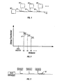
FIG. 1 shows a schematic view of a bus. -
FIG. 2 shows a graph of coupling strength. -
FIG. 3 shows a schematic view of a bus. -
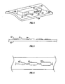
FIG. 4 shows a coupler on a bus. -
FIGS. 5 and 6 show a side view and a top view of a portion of a bus. - As shown in
FIG. 1 , in one approach to implementing a high-speedmulti-drop bus 10 usingelectromagnetic couplings devices U.S. patent application Ser. No. 09/714,899, filed Nov. 15,2000 - Controlling coupling strengths to fall uniformly within a particular range achieves a compromise between competing constraints. Excessive coupler strengths cause large impedance disturbances along the bus, thereby degrading signal integrity. High coupler strengths also divert too much signal energy into drop-
off points 24 that are closer to thebus master 30, leaving little energy to divert to distant drop-off points 28. On the other hand, insufficient coupler strength causes even the nearest drop-off points to receive or impart too little energy from or to the bus. - By using, along the bus, couplers that have deliberately non-uniform coupling strengths, bandwidth can be improved and costs reduced.
- It is useful to arrange for each device along the bus to receive the same amount of energy as any of the other devices along the bus. The amount of energy received by a device depends on both the coupling strength and the amount of energy available on the bus at the point of coupling.
- As shown in
figure 2 , eachcoupler energy coupler 42, for example, leaves a smallerremaining amount 47 of energy to reach thenext coupler 44 farther from the bus master. Because the amount of energy on the bus at the coupling location of the next coupler, e.g.,coupler 44, is lower, the coupling strength must be higher forcoupler 44 to drain thesame energy 43 as was drained by theprior coupler 42. The higher coupling strength ofcoupler 44 is tolerable because there are fewer downstream couplers that need to draw energy from the bus than was the case forcoupler 42. Conversely, weaker earlier couplers are tolerable because the full signal energy is available for them to sample, while the fact that they drain less energy benefits later couplers. - This arrangement is shown symbolically in
figure 3 in which couplers drawn using longer lines, e.g.,coupler 54 represent stronger coupling strengths, although physical dimensions are only one way of achieving this. Other examples include material properties of the coupler, for example, permittivity and permeability and the extent of the coupler along all three dimensions. The configuration of the traces may also be controlled (patterned). For example, besides zig-zags, perforated ground planes and other implementations may be used. - Using different coupler strengths along the bus reduces the cost associated with tight manufacturing tolerances, because couplers having a range of different strengths become useful. Yield increases and cost is reduced.
- A variety of mechanisms may be used for introducing and utilizing non-uniform coupler strengths for multi-drop electromagnetically coupled buses.
- In the case of variations due to the manufacturing of the couplers, the non-uniformity already exists. Mechanisms such as color coding or physical keying may be used to label or target different coupler strengths for different bus positions. A wider range of coupling strength may be tolerable in manufacturing if, after testing, weak couplers are marked or keyed for near bus positions and strong ones for far positions.
- In implementations in which manufacturing tolerances are relaxed and coupling strengths are allowed to vary more widely than would otherwise be the case, the finished couplers may be tested and sorted by coupling strength. As shown in
figure 4 , the relative coupling strengths of the couplers may be indicated by marking thecouplers 56 withcolor 58 orsymbols 60 or other indicia or devices. Any device or technique can be used which assures that couplers of the intended strength occupy intended positions along the bus. - In some cases, the system may rely on human installation in the right position based on color. In other cases, the placing of the couplers may be effected by robotic systems that could "read" color indications or bar codes or other information marked on the couplers.
- In addition, appropriate positioning of the various couplers may be enforced by providing different keyed mechanical features 62 on the couplers that correspond to the different coupling strengths. The motherboard may then be constructed to have
corresponding features 66 to accept only a particular coupler key at each position along thebus 68. - Aside from taking advantage of the natural variation in size and other parameters resulting from broad manufacturing tolerances, variations in coupler strength may be achieved more deliberately, for example, by controlling dielectric thicknesses, dielectric constants, and the number of zigzag geometry crossover points on the coupling traces of the bus and the coupler. The choice among possible mechanisms could be based on cost. For example, if the cost of engineering and manufacturing multiple categories of modules to be attached to the bus is a concern, the system may use uniform daughter cards and make alterations only to parameters of the motherboards that affect the coupling strengths at various points along the bus.
- As shown in
figure 5 (which is not to scale), variations of motherboards may includedielectric spacers motherboard 80 at the locations of drop-off points along the bus. Or the widths of motherboard coupling traces 86, 82, 84 may be different at different coupler locations, as shown onfigure 6 (also not to scale). - Wider traces would yield stronger coupling for couplers that are farther away from the bus controller. Wider traces could use either different categories of daughter cards (if the trace width variations were to be provided on the daughter cards rather than on the motherboard) or adjustment of the trace widths on the motherboard.
- The variation in impedance of the motherboard traces (resulting from different trace widths) could be offset, if desired, by progressive cross hatching. The cross-hatching may be in the form of a pattern of holes in the ground plane of the motherboard. The removal of metal changes the impedance, because the field lines terminate in different patterns than for continuous metal. More cross hatching may be provided under wider traces. The cross-hatching maintains the average overlap between the trace and the ground plane, which factors into the trace impedance, thus removing any unwanted correlation between the strength of a coupler and its standalone impedance to its own ground plane.
- Although we have described and shown some implementations of the invention as examples, other implementations of features and combinations of features are also within the scope of the following claims.
- For example, there may be applications in which it is useful to arrange the different couplers in an order such that the coupling strengths rise and/or fall other than monotonically with distance along the bus.
Claims (18)
- A method comprising
providing electromagnetic coupling locations (12, 14, 16) at coupling traces (82, 84, 86) along a bus (10) at which devices (24, 26, 28) can be respectively coupled for communication on the bus (10), and
causing electromagnetic coupling strengths associated with at least some coupling locations (12, 14, 16) to have different, selected values,
said method characterized by further steps of:arranging the bus (10) along a circuit board (80); andconfiguring internal planes within the circuit board (80) to offset impedance differences associated with the different coupling locations (12, 14, 16) along the bus (10), including providing a pattern of holes in a ground plane of the circuit board (80) to maintain an average overlap between said coupling traces (82, 84, 86) on the circuit board (80) and the ground plane. - The method of claim 1 in which the causing includes effecting differences in physical characteristics of elements of at least some of couplers (42, 44, 46) that are located at the coupling locations.
- The method of claim 1 in which the causing includes measuring electromagnetic coupling strengths of couplers (42, 44, 46) to be used at the coupling locations, and causing the couplers having different measured electromagnetic coupling strengths to occupy selected coupling locations.
- The method of claim 1 in which the different electromagnetic coupling strengths are caused by the physical characteristics of couplers (42, 44, 46) mounted on the bus (10) or by the physical characteristics of the bus (10) or by both.
- The method of claim 2 in which the physical characteristics include dimensions.
- The method of claim 2 in which the physical characteristics result from variations that occur within manufacturing tolerances.
- The method of claim 2 in which the physical characteristics include coupler geometry.
- The method of claim 7 in which the geometry includes zigzag traces.
- The method of claim 2 in which the physical characteristics include dielectric characteristics.
- The method of claim 1 in which the electromagnetic coupling strengths are caused to increase or decrease monotonically along the bus (10).
- The method of claim 1 in which the strengths are caused to have values at the locations such that essentially equal amounts of energy are drained from the bus (10) at the respective locations (12, 14, 16).
- The method of claim 10 in which the increase occurs from an end of the bus (10) to which a signal source is to be connected.
- The method of claim 12 in which the signal source comprises a bus master (30).
- The method of claim 1 also comprising providing indicia (58, 60) on elements (56) that effect the coupling strengths, and placing the elements (56) at locations along the bus (10) based on the indicia.
- The method of claim 14 in which the placing is done by hand.
- A system comprising
a circuit board (80) bearing a bus (10), and
at coupling locations (12, 14, 16) along the bus, bus elements associated with different selected coupling strengths for coupling with communicating devices (24, 26, 28),
characterized in that
the bus elements comprise coupling traces (82, 84, 86), and
a pattern of holes in a ground plane of the circuit board (80) is provided to maintain an average overlap between the coupling traces (82, 84, 86) on the circuit board (80) and the ground plane. - The system of claim 16 in which the coupling traces (82, 84, 86) have different dimensions.
- The system of claim 16 in which the bus elements comprise dielectric spacers (70, 72, 74).
Applications Claiming Priority (3)
| Application Number | Priority Date | Filing Date | Title |
|---|---|---|---|
| US165096 | 2002-06-05 | ||
| US10/165,096 US7126437B2 (en) | 2002-06-05 | 2002-06-05 | Bus signaling through electromagnetic couplers having different coupling strengths at different locations |
| PCT/US2003/017314 WO2003105427A1 (en) | 2002-06-05 | 2003-05-30 | Method and system for electromagnetically coupling devices to a bus |
Publications (2)
| Publication Number | Publication Date |
|---|---|
| EP1510053A1 EP1510053A1 (en) | 2005-03-02 |
| EP1510053B1 true EP1510053B1 (en) | 2012-07-11 |
Family
ID=29710359
Family Applications (1)
| Application Number | Title | Priority Date | Filing Date |
|---|---|---|---|
| EP03731491A Expired - Lifetime EP1510053B1 (en) | 2002-06-05 | 2003-05-30 | Method and system for electromagnetically coupling devices to a bus |
Country Status (6)
| Country | Link |
|---|---|
| US (1) | US7126437B2 (en) |
| EP (1) | EP1510053B1 (en) |
| CN (1) | CN1675905B (en) |
| AU (1) | AU2003240483A1 (en) |
| TW (1) | TWI224736B (en) |
| WO (1) | WO2003105427A1 (en) |
Families Citing this family (11)
| Publication number | Priority date | Publication date | Assignee | Title |
|---|---|---|---|---|
| US7075795B2 (en) * | 2002-02-14 | 2006-07-11 | Intel Corporation | Electromagnetic bus coupling |
| US20030152153A1 (en) * | 2002-02-14 | 2003-08-14 | Simon Thomas D. | Signaling through electromagnetic couplers |
| US7088198B2 (en) | 2002-06-05 | 2006-08-08 | Intel Corporation | Controlling coupling strength in electromagnetic bus coupling |
| US7068120B2 (en) | 2002-06-25 | 2006-06-27 | Intel Corporation | Electromagnetic bus coupling having an electromagnetic coupling interposer |
| TWI242132B (en) * | 2002-07-01 | 2005-10-21 | Renesas Tech Corp | Equal-amplitude directional coupling bus system |
| US6887095B2 (en) | 2002-12-30 | 2005-05-03 | Intel Corporation | Electromagnetic coupler registration and mating |
| DE102004032513B4 (en) * | 2004-07-06 | 2013-04-04 | Continental Teves Ag & Co. Ohg | Circuit arrangement for contactless tapping of electrical signals from at least one signal line |
| US7830225B2 (en) * | 2005-06-13 | 2010-11-09 | Gale Robert D | Electric signal splitters |
| US7375533B2 (en) * | 2005-06-15 | 2008-05-20 | Gale Robert D | Continuity tester adaptors |
| US7342466B2 (en) * | 2005-08-10 | 2008-03-11 | Intel Corporation | Hybrid coupler having resistive coupling and electromagnetic coupling |
| CN101853825B (en) * | 2009-04-03 | 2012-01-25 | 鸿富锦精密工业(深圳)有限公司 | Multi-load topology framework |
Family Cites Families (32)
| Publication number | Priority date | Publication date | Assignee | Title |
|---|---|---|---|---|
| US18526A (en) * | 1857-10-27 | Steam-pressure gkage | ||
| FR1548848A (en) | 1967-01-13 | 1968-12-06 | ||
| US3516065A (en) * | 1967-01-13 | 1970-06-02 | Ibm | Digital transmission system |
| US3673548A (en) * | 1970-10-19 | 1972-06-27 | Itt | Printed circuit board connector |
| US4192832A (en) * | 1979-01-29 | 1980-03-11 | Goettl Adam D | Automatic flushing and draining reservoir apparatus for evaporative coolers |
| US5192832A (en) | 1990-08-31 | 1993-03-09 | Amp Incorporated | Electromagnet insert for data current coupler |
| US5363071A (en) * | 1993-05-04 | 1994-11-08 | Motorola, Inc. | Apparatus and method for varying the coupling of a radio frequency signal |
| US5432486A (en) * | 1993-05-20 | 1995-07-11 | Northern Telecom Limited | Capacitive and inductive coupling connector |
| JP3399630B2 (en) * | 1993-09-27 | 2003-04-21 | 株式会社日立製作所 | Bus system |
| CN2286322Y (en) * | 1996-12-13 | 1998-07-15 | 李曦 | Chromatic circle resistance direct-reading card |
| US5958030A (en) * | 1996-12-27 | 1999-09-28 | Nortel Networks Corporation | Intra-shelf free space interconnect |
| AUPO546797A0 (en) * | 1997-03-05 | 1997-03-27 | Commonwealth Scientific And Industrial Research Organisation | A high frequency multi-port switching circuit |
| JP3543555B2 (en) * | 1997-08-08 | 2004-07-14 | 株式会社日立製作所 | Signal transmission equipment |
| US6111476A (en) * | 1998-12-21 | 2000-08-29 | Nortel Networks Corporation | Non-contact coupling system |
| JP3820843B2 (en) * | 1999-05-12 | 2006-09-13 | 株式会社日立製作所 | Directional coupled memory module |
| US6449308B1 (en) | 1999-05-25 | 2002-09-10 | Intel Corporation | High-speed digital distribution system |
| US6576847B2 (en) * | 1999-05-25 | 2003-06-10 | Intel Corporation | Clamp to secure carrier to device for electromagnetic coupler |
| US6697420B1 (en) * | 1999-05-25 | 2004-02-24 | Intel Corporation | Symbol-based signaling for an electromagnetically-coupled bus system |
| US6498305B1 (en) * | 1999-05-25 | 2002-12-24 | Intel Corporation | Interconnect mechanics for electromagnetic coupler |
| US6625682B1 (en) * | 1999-05-25 | 2003-09-23 | Intel Corporation | Electromagnetically-coupled bus system |
| US6434647B1 (en) | 1999-05-27 | 2002-08-13 | Microsoft Corporation | Reflected-wave bus termination |
| US6335662B1 (en) * | 1999-09-21 | 2002-01-01 | The United States Of America As Represented By The Secretary Of The Army | Ferroelectric-tunable microwave branching couplers |
| US6399898B1 (en) * | 1999-11-18 | 2002-06-04 | Nortel Networks Limited | Technique for coupling signals between circuit boards |
| TW530248B (en) | 2000-08-09 | 2003-05-01 | Hitachi Ltd | Data transmission system of directional coupling type using forward wave and reflective wave |
| DE10055090A1 (en) * | 2000-11-07 | 2002-05-08 | Conducta Endress & Hauser | Plug-in connector for connecting a transmission line to at least one sensor, has arrangement for implementing contactless signal transfer between plug element and socket element |
| US6573801B1 (en) * | 2000-11-15 | 2003-06-03 | Intel Corporation | Electromagnetic coupler |
| US6437647B1 (en) * | 2001-01-30 | 2002-08-20 | Conexant Systems, Inc. | Current mirror compensation system for power amplifiers |
| US6882239B2 (en) * | 2001-05-08 | 2005-04-19 | Formfactor, Inc. | Electromagnetically coupled interconnect system |
| US7075795B2 (en) * | 2002-02-14 | 2006-07-11 | Intel Corporation | Electromagnetic bus coupling |
| US20030152153A1 (en) * | 2002-02-14 | 2003-08-14 | Simon Thomas D. | Signaling through electromagnetic couplers |
| US7088198B2 (en) * | 2002-06-05 | 2006-08-08 | Intel Corporation | Controlling coupling strength in electromagnetic bus coupling |
| US7068120B2 (en) * | 2002-06-25 | 2006-06-27 | Intel Corporation | Electromagnetic bus coupling having an electromagnetic coupling interposer |
-
2002
- 2002-06-05 US US10/165,096 patent/US7126437B2/en not_active Expired - Fee Related
-
2003
- 2003-05-30 EP EP03731491A patent/EP1510053B1/en not_active Expired - Lifetime
- 2003-05-30 AU AU2003240483A patent/AU2003240483A1/en not_active Abandoned
- 2003-05-30 WO PCT/US2003/017314 patent/WO2003105427A1/en not_active Application Discontinuation
- 2003-05-30 CN CN03818822.8A patent/CN1675905B/en not_active Expired - Fee Related
- 2003-06-03 TW TW092115082A patent/TWI224736B/en not_active IP Right Cessation
Also Published As
| Publication number | Publication date |
|---|---|
| TW200407714A (en) | 2004-05-16 |
| US7126437B2 (en) | 2006-10-24 |
| EP1510053A1 (en) | 2005-03-02 |
| US20030227346A1 (en) | 2003-12-11 |
| CN1675905B (en) | 2010-12-08 |
| CN1675905A (en) | 2005-09-28 |
| TWI224736B (en) | 2004-12-01 |
| AU2003240483A1 (en) | 2003-12-22 |
| WO2003105427A1 (en) | 2003-12-18 |
Similar Documents
| Publication | Publication Date | Title |
|---|---|---|
| EP1510053B1 (en) | Method and system for electromagnetically coupling devices to a bus | |
| DE69838364T2 (en) | Read / write device, power supply system and communication system | |
| CN101378145B (en) | Tag antenna and tag | |
| DE102008051948B4 (en) | Integrated circuit component comprising a contactless integrated circuit insert | |
| EP2883273B1 (en) | Electrical connector housing having an rfid transponder | |
| JP4711692B2 (en) | Meander line antenna | |
| CN107069191B (en) | Antenna assembly and electronic equipment | |
| DE102010024439B4 (en) | antenna device | |
| CN101079515B (en) | Radio frequency identification tag and antenna for radio frequency identification tag | |
| JP2003522386A (en) | High-speed pressure connector | |
| CN101714696B (en) | Antenna and reader/writer device | |
| EP1912284A1 (en) | Rf tag and rf tag manufacturing method | |
| KR100860448B1 (en) | Flat coil component, characteristic adjusting method of flat coil component, id tag, and characteristic adjusting method of id tag | |
| PL2266808T3 (en) | Spatially selective UHF near field microstrip coupler device and RFID systems using device | |
| CN101577361A (en) | Method for manufacturing near field communication (NFC) terminal and antenna thereof | |
| CN102326174A (en) | RFID assembling and attachment method and device | |
| CN101904050A (en) | Antenna device and wireless communication device using the same | |
| CN101253653A (en) | RF label and method for manufacturing RF label | |
| EP2333691B1 (en) | Optical or electrical cable for connecting two devices | |
| DE112009002384B4 (en) | Antenna and wireless IC component | |
| CN104078745A (en) | Antenna assembly | |
| WO2005022445A3 (en) | Spatially selective uhf near field microstrip coupler device and rfid systems using device | |
| DE602006001034T2 (en) | Radio transmission system, antenna device and method for sheet processing | |
| DE102006001005A1 (en) | Radio frequency identification transponder adapting method for wireless identification system, involves determining position of chip based on measured and simulation values, and arranging and contacting chip with matching network | |
| DE102013101622B4 (en) | READING/WRITING DEVICE FOR CHIP CARDS |
Legal Events
| Date | Code | Title | Description |
|---|---|---|---|
| PUAI | Public reference made under article 153(3) epc to a published international application that has entered the european phase |
Free format text: ORIGINAL CODE: 0009012 |
|
| 17P | Request for examination filed |
Effective date: 20041111 |
|
| AK | Designated contracting states |
Kind code of ref document: A1 Designated state(s): AT BE BG CH CY CZ DE DK EE ES FI FR GB GR HU IE IT LI LU MC NL PT RO SE SI SK TR |
|
| AX | Request for extension of the european patent |
Extension state: AL LT LV MK |
|
| RIN1 | Information on inventor provided before grant (corrected) |
Inventor name: BENHAM, JOHN Inventor name: AMIRTHARAJAH, RAJEEVAN Inventor name: SIMON, THOMAS |
|
| DAX | Request for extension of the european patent (deleted) | ||
| 17Q | First examination report despatched |
Effective date: 20100706 |
|
| REG | Reference to a national code |
Ref country code: DE Ref legal event code: R079 Ref document number: 60341516 Country of ref document: DE Free format text: PREVIOUS MAIN CLASS: H04L0025020000 Ipc: H01P0005180000 |
|
| RIC1 | Information provided on ipc code assigned before grant |
Ipc: H04L 12/403 20060101ALI20111104BHEP Ipc: H01P 5/18 20060101AFI20111104BHEP Ipc: H04L 25/02 20060101ALI20111104BHEP |
|
| GRAP | Despatch of communication of intention to grant a patent |
Free format text: ORIGINAL CODE: EPIDOSNIGR1 |
|
| GRAS | Grant fee paid |
Free format text: ORIGINAL CODE: EPIDOSNIGR3 |
|
| GRAA | (expected) grant |
Free format text: ORIGINAL CODE: 0009210 |
|
| AK | Designated contracting states |
Kind code of ref document: B1 Designated state(s): AT BE BG CH CY CZ DE DK EE ES FI FR GB GR HU IE IT LI LU MC NL PT RO SE SI SK TR |
|
| REG | Reference to a national code |
Ref country code: GB Ref legal event code: FG4D |
|
| REG | Reference to a national code |
Ref country code: CH Ref legal event code: EP |
|
| REG | Reference to a national code |
Ref country code: AT Ref legal event code: REF Ref document number: 566526 Country of ref document: AT Kind code of ref document: T Effective date: 20120715 |
|
| REG | Reference to a national code |
Ref country code: IE Ref legal event code: FG4D |
|
| REG | Reference to a national code |
Ref country code: DE Ref legal event code: R096 Ref document number: 60341516 Country of ref document: DE Effective date: 20120830 |
|
| REG | Reference to a national code |
Ref country code: NL Ref legal event code: VDEP Effective date: 20120711 |
|
| REG | Reference to a national code |
Ref country code: AT Ref legal event code: MK05 Ref document number: 566526 Country of ref document: AT Kind code of ref document: T Effective date: 20120711 |
|
| PG25 | Lapsed in a contracting state [announced via postgrant information from national office to epo] |
Ref country code: AT Free format text: LAPSE BECAUSE OF FAILURE TO SUBMIT A TRANSLATION OF THE DESCRIPTION OR TO PAY THE FEE WITHIN THE PRESCRIBED TIME-LIMIT Effective date: 20120711 Ref country code: BE Free format text: LAPSE BECAUSE OF FAILURE TO SUBMIT A TRANSLATION OF THE DESCRIPTION OR TO PAY THE FEE WITHIN THE PRESCRIBED TIME-LIMIT Effective date: 20120711 Ref country code: FI Free format text: LAPSE BECAUSE OF FAILURE TO SUBMIT A TRANSLATION OF THE DESCRIPTION OR TO PAY THE FEE WITHIN THE PRESCRIBED TIME-LIMIT Effective date: 20120711 Ref country code: CY Free format text: LAPSE BECAUSE OF FAILURE TO SUBMIT A TRANSLATION OF THE DESCRIPTION OR TO PAY THE FEE WITHIN THE PRESCRIBED TIME-LIMIT Effective date: 20120711 |
|
| PG25 | Lapsed in a contracting state [announced via postgrant information from national office to epo] |
Ref country code: PT Free format text: LAPSE BECAUSE OF FAILURE TO SUBMIT A TRANSLATION OF THE DESCRIPTION OR TO PAY THE FEE WITHIN THE PRESCRIBED TIME-LIMIT Effective date: 20121112 Ref country code: SI Free format text: LAPSE BECAUSE OF FAILURE TO SUBMIT A TRANSLATION OF THE DESCRIPTION OR TO PAY THE FEE WITHIN THE PRESCRIBED TIME-LIMIT Effective date: 20120711 Ref country code: SE Free format text: LAPSE BECAUSE OF FAILURE TO SUBMIT A TRANSLATION OF THE DESCRIPTION OR TO PAY THE FEE WITHIN THE PRESCRIBED TIME-LIMIT Effective date: 20120711 Ref country code: GR Free format text: LAPSE BECAUSE OF FAILURE TO SUBMIT A TRANSLATION OF THE DESCRIPTION OR TO PAY THE FEE WITHIN THE PRESCRIBED TIME-LIMIT Effective date: 20121012 |
|
| PG25 | Lapsed in a contracting state [announced via postgrant information from national office to epo] |
Ref country code: NL Free format text: LAPSE BECAUSE OF FAILURE TO SUBMIT A TRANSLATION OF THE DESCRIPTION OR TO PAY THE FEE WITHIN THE PRESCRIBED TIME-LIMIT Effective date: 20120711 |
|
| PG25 | Lapsed in a contracting state [announced via postgrant information from national office to epo] |
Ref country code: ES Free format text: LAPSE BECAUSE OF FAILURE TO SUBMIT A TRANSLATION OF THE DESCRIPTION OR TO PAY THE FEE WITHIN THE PRESCRIBED TIME-LIMIT Effective date: 20121022 Ref country code: EE Free format text: LAPSE BECAUSE OF FAILURE TO SUBMIT A TRANSLATION OF THE DESCRIPTION OR TO PAY THE FEE WITHIN THE PRESCRIBED TIME-LIMIT Effective date: 20120711 Ref country code: CZ Free format text: LAPSE BECAUSE OF FAILURE TO SUBMIT A TRANSLATION OF THE DESCRIPTION OR TO PAY THE FEE WITHIN THE PRESCRIBED TIME-LIMIT Effective date: 20120711 Ref country code: DK Free format text: LAPSE BECAUSE OF FAILURE TO SUBMIT A TRANSLATION OF THE DESCRIPTION OR TO PAY THE FEE WITHIN THE PRESCRIBED TIME-LIMIT Effective date: 20120711 Ref country code: RO Free format text: LAPSE BECAUSE OF FAILURE TO SUBMIT A TRANSLATION OF THE DESCRIPTION OR TO PAY THE FEE WITHIN THE PRESCRIBED TIME-LIMIT Effective date: 20120711 |
|
| PLBE | No opposition filed within time limit |
Free format text: ORIGINAL CODE: 0009261 |
|
| STAA | Information on the status of an ep patent application or granted ep patent |
Free format text: STATUS: NO OPPOSITION FILED WITHIN TIME LIMIT |
|
| PG25 | Lapsed in a contracting state [announced via postgrant information from national office to epo] |
Ref country code: IT Free format text: LAPSE BECAUSE OF FAILURE TO SUBMIT A TRANSLATION OF THE DESCRIPTION OR TO PAY THE FEE WITHIN THE PRESCRIBED TIME-LIMIT Effective date: 20120711 Ref country code: SK Free format text: LAPSE BECAUSE OF FAILURE TO SUBMIT A TRANSLATION OF THE DESCRIPTION OR TO PAY THE FEE WITHIN THE PRESCRIBED TIME-LIMIT Effective date: 20120711 |
|
| 26N | No opposition filed |
Effective date: 20130412 |
|
| PG25 | Lapsed in a contracting state [announced via postgrant information from national office to epo] |
Ref country code: BG Free format text: LAPSE BECAUSE OF FAILURE TO SUBMIT A TRANSLATION OF THE DESCRIPTION OR TO PAY THE FEE WITHIN THE PRESCRIBED TIME-LIMIT Effective date: 20121011 |
|
| REG | Reference to a national code |
Ref country code: DE Ref legal event code: R097 Ref document number: 60341516 Country of ref document: DE Effective date: 20130412 |
|
| PG25 | Lapsed in a contracting state [announced via postgrant information from national office to epo] |
Ref country code: MC Free format text: LAPSE BECAUSE OF FAILURE TO SUBMIT A TRANSLATION OF THE DESCRIPTION OR TO PAY THE FEE WITHIN THE PRESCRIBED TIME-LIMIT Effective date: 20120711 |
|
| REG | Reference to a national code |
Ref country code: CH Ref legal event code: PL |
|
| PG25 | Lapsed in a contracting state [announced via postgrant information from national office to epo] |
Ref country code: CH Free format text: LAPSE BECAUSE OF NON-PAYMENT OF DUE FEES Effective date: 20130531 Ref country code: LI Free format text: LAPSE BECAUSE OF NON-PAYMENT OF DUE FEES Effective date: 20130531 |
|
| REG | Reference to a national code |
Ref country code: IE Ref legal event code: MM4A |
|
| REG | Reference to a national code |
Ref country code: FR Ref legal event code: ST Effective date: 20140131 |
|
| PG25 | Lapsed in a contracting state [announced via postgrant information from national office to epo] |
Ref country code: IE Free format text: LAPSE BECAUSE OF NON-PAYMENT OF DUE FEES Effective date: 20130530 |
|
| PG25 | Lapsed in a contracting state [announced via postgrant information from national office to epo] |
Ref country code: FR Free format text: LAPSE BECAUSE OF NON-PAYMENT OF DUE FEES Effective date: 20130531 |
|
| PG25 | Lapsed in a contracting state [announced via postgrant information from national office to epo] |
Ref country code: TR Free format text: LAPSE BECAUSE OF FAILURE TO SUBMIT A TRANSLATION OF THE DESCRIPTION OR TO PAY THE FEE WITHIN THE PRESCRIBED TIME-LIMIT Effective date: 20120711 |
|
| PG25 | Lapsed in a contracting state [announced via postgrant information from national office to epo] |
Ref country code: HU Free format text: LAPSE BECAUSE OF FAILURE TO SUBMIT A TRANSLATION OF THE DESCRIPTION OR TO PAY THE FEE WITHIN THE PRESCRIBED TIME-LIMIT; INVALID AB INITIO Effective date: 20030530 Ref country code: LU Free format text: LAPSE BECAUSE OF NON-PAYMENT OF DUE FEES Effective date: 20130530 |
|
| PGFP | Annual fee paid to national office [announced via postgrant information from national office to epo] |
Ref country code: DE Payment date: 20160524 Year of fee payment: 14 Ref country code: GB Payment date: 20160525 Year of fee payment: 14 |
|
| REG | Reference to a national code |
Ref country code: DE Ref legal event code: R119 Ref document number: 60341516 Country of ref document: DE |
|
| GBPC | Gb: european patent ceased through non-payment of renewal fee |
Effective date: 20170530 |
|
| PG25 | Lapsed in a contracting state [announced via postgrant information from national office to epo] |
Ref country code: GB Free format text: LAPSE BECAUSE OF NON-PAYMENT OF DUE FEES Effective date: 20170530 Ref country code: DE Free format text: LAPSE BECAUSE OF NON-PAYMENT OF DUE FEES Effective date: 20171201 |