EP1493797A1 - Organic electroluminescence element - Google Patents
Organic electroluminescence element Download PDFInfo
- Publication number
- EP1493797A1 EP1493797A1 EP03715461A EP03715461A EP1493797A1 EP 1493797 A1 EP1493797 A1 EP 1493797A1 EP 03715461 A EP03715461 A EP 03715461A EP 03715461 A EP03715461 A EP 03715461A EP 1493797 A1 EP1493797 A1 EP 1493797A1
- Authority
- EP
- European Patent Office
- Prior art keywords
- organic
- electroluminescence device
- structural formula
- organic electroluminescence
- guest material
- Prior art date
- Legal status (The legal status is an assumption and is not a legal conclusion. Google has not performed a legal analysis and makes no representation as to the accuracy of the status listed.)
- Granted
Links
Images


Classifications
-
- C—CHEMISTRY; METALLURGY
- C09—DYES; PAINTS; POLISHES; NATURAL RESINS; ADHESIVES; COMPOSITIONS NOT OTHERWISE PROVIDED FOR; APPLICATIONS OF MATERIALS NOT OTHERWISE PROVIDED FOR
- C09K—MATERIALS FOR MISCELLANEOUS APPLICATIONS, NOT PROVIDED FOR ELSEWHERE
- C09K11/00—Luminescent, e.g. electroluminescent, chemiluminescent materials
- C09K11/06—Luminescent, e.g. electroluminescent, chemiluminescent materials containing organic luminescent materials
-
- H—ELECTRICITY
- H10—SEMICONDUCTOR DEVICES; ELECTRIC SOLID-STATE DEVICES NOT OTHERWISE PROVIDED FOR
- H10K—ORGANIC ELECTRIC SOLID-STATE DEVICES
- H10K85/00—Organic materials used in the body or electrodes of devices covered by this subclass
- H10K85/30—Coordination compounds
- H10K85/321—Metal complexes comprising a group IIIA element, e.g. Tris (8-hydroxyquinoline) gallium [Gaq3]
-
- C—CHEMISTRY; METALLURGY
- C09—DYES; PAINTS; POLISHES; NATURAL RESINS; ADHESIVES; COMPOSITIONS NOT OTHERWISE PROVIDED FOR; APPLICATIONS OF MATERIALS NOT OTHERWISE PROVIDED FOR
- C09K—MATERIALS FOR MISCELLANEOUS APPLICATIONS, NOT PROVIDED FOR ELSEWHERE
- C09K2211/00—Chemical nature of organic luminescent or tenebrescent compounds
- C09K2211/10—Non-macromolecular compounds
- C09K2211/1003—Carbocyclic compounds
- C09K2211/1007—Non-condensed systems
-
- C—CHEMISTRY; METALLURGY
- C09—DYES; PAINTS; POLISHES; NATURAL RESINS; ADHESIVES; COMPOSITIONS NOT OTHERWISE PROVIDED FOR; APPLICATIONS OF MATERIALS NOT OTHERWISE PROVIDED FOR
- C09K—MATERIALS FOR MISCELLANEOUS APPLICATIONS, NOT PROVIDED FOR ELSEWHERE
- C09K2211/00—Chemical nature of organic luminescent or tenebrescent compounds
- C09K2211/10—Non-macromolecular compounds
- C09K2211/1003—Carbocyclic compounds
- C09K2211/1011—Condensed systems
-
- C—CHEMISTRY; METALLURGY
- C09—DYES; PAINTS; POLISHES; NATURAL RESINS; ADHESIVES; COMPOSITIONS NOT OTHERWISE PROVIDED FOR; APPLICATIONS OF MATERIALS NOT OTHERWISE PROVIDED FOR
- C09K—MATERIALS FOR MISCELLANEOUS APPLICATIONS, NOT PROVIDED FOR ELSEWHERE
- C09K2211/00—Chemical nature of organic luminescent or tenebrescent compounds
- C09K2211/10—Non-macromolecular compounds
- C09K2211/1003—Carbocyclic compounds
- C09K2211/1014—Carbocyclic compounds bridged by heteroatoms, e.g. N, P, Si or B
-
- C—CHEMISTRY; METALLURGY
- C09—DYES; PAINTS; POLISHES; NATURAL RESINS; ADHESIVES; COMPOSITIONS NOT OTHERWISE PROVIDED FOR; APPLICATIONS OF MATERIALS NOT OTHERWISE PROVIDED FOR
- C09K—MATERIALS FOR MISCELLANEOUS APPLICATIONS, NOT PROVIDED FOR ELSEWHERE
- C09K2211/00—Chemical nature of organic luminescent or tenebrescent compounds
- C09K2211/10—Non-macromolecular compounds
- C09K2211/1018—Heterocyclic compounds
- C09K2211/1025—Heterocyclic compounds characterised by ligands
- C09K2211/1029—Heterocyclic compounds characterised by ligands containing one nitrogen atom as the heteroatom
- C09K2211/1037—Heterocyclic compounds characterised by ligands containing one nitrogen atom as the heteroatom with sulfur
-
- C—CHEMISTRY; METALLURGY
- C09—DYES; PAINTS; POLISHES; NATURAL RESINS; ADHESIVES; COMPOSITIONS NOT OTHERWISE PROVIDED FOR; APPLICATIONS OF MATERIALS NOT OTHERWISE PROVIDED FOR
- C09K—MATERIALS FOR MISCELLANEOUS APPLICATIONS, NOT PROVIDED FOR ELSEWHERE
- C09K2211/00—Chemical nature of organic luminescent or tenebrescent compounds
- C09K2211/10—Non-macromolecular compounds
- C09K2211/1018—Heterocyclic compounds
- C09K2211/1025—Heterocyclic compounds characterised by ligands
- C09K2211/1044—Heterocyclic compounds characterised by ligands containing two nitrogen atoms as heteroatoms
- C09K2211/1048—Heterocyclic compounds characterised by ligands containing two nitrogen atoms as heteroatoms with oxygen
-
- C—CHEMISTRY; METALLURGY
- C09—DYES; PAINTS; POLISHES; NATURAL RESINS; ADHESIVES; COMPOSITIONS NOT OTHERWISE PROVIDED FOR; APPLICATIONS OF MATERIALS NOT OTHERWISE PROVIDED FOR
- C09K—MATERIALS FOR MISCELLANEOUS APPLICATIONS, NOT PROVIDED FOR ELSEWHERE
- C09K2211/00—Chemical nature of organic luminescent or tenebrescent compounds
- C09K2211/10—Non-macromolecular compounds
- C09K2211/1018—Heterocyclic compounds
- C09K2211/1025—Heterocyclic compounds characterised by ligands
- C09K2211/1092—Heterocyclic compounds characterised by ligands containing sulfur as the only heteroatom
-
- C—CHEMISTRY; METALLURGY
- C09—DYES; PAINTS; POLISHES; NATURAL RESINS; ADHESIVES; COMPOSITIONS NOT OTHERWISE PROVIDED FOR; APPLICATIONS OF MATERIALS NOT OTHERWISE PROVIDED FOR
- C09K—MATERIALS FOR MISCELLANEOUS APPLICATIONS, NOT PROVIDED FOR ELSEWHERE
- C09K2211/00—Chemical nature of organic luminescent or tenebrescent compounds
- C09K2211/18—Metal complexes
- C09K2211/185—Metal complexes of the platinum group, i.e. Os, Ir, Pt, Ru, Rh or Pd
-
- C—CHEMISTRY; METALLURGY
- C09—DYES; PAINTS; POLISHES; NATURAL RESINS; ADHESIVES; COMPOSITIONS NOT OTHERWISE PROVIDED FOR; APPLICATIONS OF MATERIALS NOT OTHERWISE PROVIDED FOR
- C09K—MATERIALS FOR MISCELLANEOUS APPLICATIONS, NOT PROVIDED FOR ELSEWHERE
- C09K2211/00—Chemical nature of organic luminescent or tenebrescent compounds
- C09K2211/18—Metal complexes
- C09K2211/186—Metal complexes of the light metals other than alkali metals and alkaline earth metals, i.e. Be, Al or Mg
-
- C—CHEMISTRY; METALLURGY
- C09—DYES; PAINTS; POLISHES; NATURAL RESINS; ADHESIVES; COMPOSITIONS NOT OTHERWISE PROVIDED FOR; APPLICATIONS OF MATERIALS NOT OTHERWISE PROVIDED FOR
- C09K—MATERIALS FOR MISCELLANEOUS APPLICATIONS, NOT PROVIDED FOR ELSEWHERE
- C09K2211/00—Chemical nature of organic luminescent or tenebrescent compounds
- C09K2211/18—Metal complexes
- C09K2211/188—Metal complexes of other metals not provided for in one of the previous groups
-
- H—ELECTRICITY
- H10—SEMICONDUCTOR DEVICES; ELECTRIC SOLID-STATE DEVICES NOT OTHERWISE PROVIDED FOR
- H10K—ORGANIC ELECTRIC SOLID-STATE DEVICES
- H10K2101/00—Properties of the organic materials covered by group H10K85/00
- H10K2101/10—Triplet emission
-
- H—ELECTRICITY
- H10—SEMICONDUCTOR DEVICES; ELECTRIC SOLID-STATE DEVICES NOT OTHERWISE PROVIDED FOR
- H10K—ORGANIC ELECTRIC SOLID-STATE DEVICES
- H10K50/00—Organic light-emitting devices
- H10K50/10—OLEDs or polymer light-emitting diodes [PLED]
- H10K50/11—OLEDs or polymer light-emitting diodes [PLED] characterised by the electroluminescent [EL] layers
-
- H—ELECTRICITY
- H10—SEMICONDUCTOR DEVICES; ELECTRIC SOLID-STATE DEVICES NOT OTHERWISE PROVIDED FOR
- H10K—ORGANIC ELECTRIC SOLID-STATE DEVICES
- H10K85/00—Organic materials used in the body or electrodes of devices covered by this subclass
- H10K85/30—Coordination compounds
-
- H—ELECTRICITY
- H10—SEMICONDUCTOR DEVICES; ELECTRIC SOLID-STATE DEVICES NOT OTHERWISE PROVIDED FOR
- H10K—ORGANIC ELECTRIC SOLID-STATE DEVICES
- H10K85/00—Organic materials used in the body or electrodes of devices covered by this subclass
- H10K85/30—Coordination compounds
- H10K85/341—Transition metal complexes, e.g. Ru(II)polypyridine complexes
- H10K85/342—Transition metal complexes, e.g. Ru(II)polypyridine complexes comprising iridium
-
- H—ELECTRICITY
- H10—SEMICONDUCTOR DEVICES; ELECTRIC SOLID-STATE DEVICES NOT OTHERWISE PROVIDED FOR
- H10K—ORGANIC ELECTRIC SOLID-STATE DEVICES
- H10K85/00—Organic materials used in the body or electrodes of devices covered by this subclass
- H10K85/60—Organic compounds having low molecular weight
- H10K85/615—Polycyclic condensed aromatic hydrocarbons, e.g. anthracene
-
- H—ELECTRICITY
- H10—SEMICONDUCTOR DEVICES; ELECTRIC SOLID-STATE DEVICES NOT OTHERWISE PROVIDED FOR
- H10K—ORGANIC ELECTRIC SOLID-STATE DEVICES
- H10K85/00—Organic materials used in the body or electrodes of devices covered by this subclass
- H10K85/60—Organic compounds having low molecular weight
- H10K85/631—Amine compounds having at least two aryl rest on at least one amine-nitrogen atom, e.g. triphenylamine
-
- H—ELECTRICITY
- H10—SEMICONDUCTOR DEVICES; ELECTRIC SOLID-STATE DEVICES NOT OTHERWISE PROVIDED FOR
- H10K—ORGANIC ELECTRIC SOLID-STATE DEVICES
- H10K85/00—Organic materials used in the body or electrodes of devices covered by this subclass
- H10K85/60—Organic compounds having low molecular weight
- H10K85/649—Aromatic compounds comprising a hetero atom
- H10K85/656—Aromatic compounds comprising a hetero atom comprising two or more different heteroatoms per ring
- H10K85/6565—Oxadiazole compounds
-
- Y—GENERAL TAGGING OF NEW TECHNOLOGICAL DEVELOPMENTS; GENERAL TAGGING OF CROSS-SECTIONAL TECHNOLOGIES SPANNING OVER SEVERAL SECTIONS OF THE IPC; TECHNICAL SUBJECTS COVERED BY FORMER USPC CROSS-REFERENCE ART COLLECTIONS [XRACs] AND DIGESTS
- Y10—TECHNICAL SUBJECTS COVERED BY FORMER USPC
- Y10S—TECHNICAL SUBJECTS COVERED BY FORMER USPC CROSS-REFERENCE ART COLLECTIONS [XRACs] AND DIGESTS
- Y10S428/00—Stock material or miscellaneous articles
- Y10S428/917—Electroluminescent
Definitions
- the present invention relates to an organic electroluminescence device (hereinafter referred to as an organic EL device) utilizing electroluminescence of an organic compound that emits light by current injection, and having a light emitting layer in which the substance is formed in a layered state.
- an organic EL device organic electroluminescence device
- each of organic EL devices using an organic material and constituting a display panel has a structure in that an anode as a transparent electrode, plural organicmaterial layers including an organic light emitting layer and a cathode comprising a metal electrode are successively layered each as a thin film on a glass substrate as a display surface.
- the organic material layer includes a layer comprising a material having a hole transportability such as a hole injection layer and a hole transport layer, and a layer comprising a material having electron transportability such as an electron transport layer and an electron injection layer, and an organic EL device of a constitution provided with them has also been proposed.
- the electron injection layer also contains an in organic compound.
- an organic EL device of a stacked body of an organic light emitting layer and an electron or hole transport layer When an electric field is applied to an organic EL device of a stacked body of an organic light emitting layer and an electron or hole transport layer, holes are injected from the anode and electrons are injected from the cathode.
- the organic EL divide utilizes emission of light that is emitted when the electrons and the holes are recombined in the organic light emitting layer to form exciters and they are returned to the ground state.
- a dye is sometimes doped as a guest material to the light emitting layer.
- hole transporting materials capable of transporting holes have been used for the light emitting layer host material and materials having higher ionizing potential energy (Ip) than the post material of the light emitting layer such as phenanthroline derivatives, for example, 2,9-dimethyl-4,7-diphenyl-1,10-phenanthroline, i.e., BCP or aluminum chelate complex, for example, ((1,1'-biphenyl)-4-olato)bis(2-methyl-8-quinolinolato NI, 08) aluminum, i.e., BAlq are used as the hole blocking layer in the layer adjacent cathode of the light emitting layer.
- BCP ionizing potential energy
- BAlq is excellent in durability but has a drawback of poor hole blocking ability since Ip is not sufficiently high. Accordingly, in a case of using BAlq as the hole blocking layer and tris(8-hydroxyquinolateo N1, 08) aluminum, i.e., Alq3 as the electron transport layer, the electron transport layer emits light. In the organic electroluminescence device utilizing red phosphorescence emission, the emission of Alq3 (green) results in deterioration of chromaticity (orange instead of red).
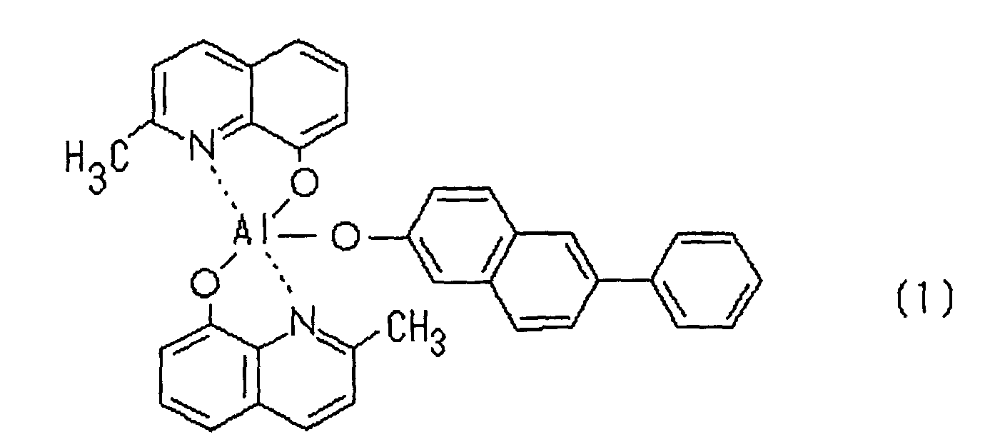
- An organic electroluminescence device is an organic electroluminescence device obtained by stacking an anode, a hole transport layer comprising an organic compound, a light emitting layer comprising an organic compound, an electron transport layer comprising an organic compound and a cathode characterized in that the light emitting layer comprises an organic host material represented by the following structural formula (1): and a phosphorescent organic guest material.
- the electroluminescence device according to the invention is characterized in that a hole injection layer is provided between the anode and the hole transportation.
- the electroluminescence device according to the invention is characterized in that an electron injection layer is provided between the cathode and the electron transport layer.
- M represents a metal, a metal oxide or a metal halide
- R represents hydrogen, alkyl, aralkyl, aryl or alkalyl. or a halogenated substitu
- the organic electroluminescence device according to the invention is characterized in that M in the phosphorescent organic guest material is platinum.
- the organic electroluminescence device is characterized in that the phosphorescent organic guest material comprises a compound represented by the following structural formula (3): (in the structural formula (3), M represents a metal, R 1 to R 8 each independently includes a hydrogen atom, alkyl group, oxy group, amino group or a hydrocarbon group having at least one carbon atom in the substituent, the number of carbon atoms is 1 to 10 in each of the hydrocarbon moieties, further, R 1 to R 8 can be selected independently from cyano, halogen, and ⁇ -haloalkyl, ⁇ -haloalkoxy, amide, sulfonyl, carbonyl, carbonyloxy and oxycarbonyl substituents containing 10 or less carbon atom and, further, R 1 together with R 2 , R 2 together with R 3 , R 3 together with R 4 , R 5 together with R 6 , R 6 together with R 7 , or R 7 together with R 8 can form a condensed benzo ring).
- M represents a metal
- the organic electroluminescence device according to the invention is characterized in that M for the phosphorescent organic guest material is iridium.
- the organic electroluminescence device is characterized in that the phosphorescent organic guest material comprises a compound represented by the following structural formula (4): (in the structural formula (4), M represents a metal, R 1 to R 6 each independently includes a hydrogen atom, alkyl group, oxy group, amino group, or a hydrocarbon group having at least one carbon atom in the substituent, the number of carbon atoms is 1 to 10 in each of the hydrocarbon moieties, further, R 1 to R 6 can be selected independently from cyano, halogen, and ⁇ -haloalkyl, ⁇ -haloalkoxy, amide, sulfonyl, carbonyl, carbonyloxy and oxycarbonyl substituents containing 10 or less of carbon atoms and, further, R 1 together with R 2 , R 3 together with R 4 , R 4 together with R 5 , or R 5 together with R 6 can form a condensed benzo ring).
- M represents a metal
- R 1 to R 6 each independently includes
- the organic electroluminescence device according to the invention is characterized in that M in the phosphorescent organic guest material is iridium.
- the organic electroluminescence device is characterized in that the phosphorescent organic guest material comprises a compound represented by the following structural formula (5): (in the structural formula (5), M represents a metal, X 1 and X 2 each independently represents an oxygen atom or a sulfur atom, R 1 to R 11 each independently includes a hydrogen atom, alkyl group, oxy group, amino group, or a hydrocarbon group having at least one carbon atom in the substituent, the number of carbon atoms is 1 to 10 in each of the hydrocarbon moieties, further, R 1 to R 11 can be selected independently from cyano, halogen, and ⁇ -haloalkyl, ⁇ -haloalkoxy, amide, sulfonyl, carbonyl, carbonyloxy and oxycarbonyl substituents containing 10 or less carbon atoms and, further, R 1 together with R 2 , R 2 together with R 3 , R 3 together with R 4 , R 5 together with R 6 or R 6 together with R 7
- the organic electroluminescence device according to the invention is characterized in that M for the phosphorescent organic guest material is iridium.
- the organic electroluminescence device is characterized in that the phosphorescent organic guest material comprises a compound represented by the following structural formula (6): (in the structural formula (6), M represents a metal, X 1 and X 2 each independently represents an oxygen atom or a sulfur atom, R 1 to R 9 each independently includes a hydrogen atom, alkyl group, oxy group, amino group or a hydrocarbon group having at least one carbon atom in the substituent, the number of carbon atoms is 1 to 10 in each of the hydrocarbon moieties, further, R 1 to R 9 can be selected independently from cyano, halogen, and ⁇ -haloalkyl, ⁇ -haloalkoxy, amide, sulfonyl, carbonyl, carbonyloxy and oxycarbonyl substituents containing 10 or less of carbon atoms and, further, R 1 together with R 2 , R 3 together with R 4 , R 4 together with R 5 , R 5 together with R 6 , R 7 together with R 8
- the organic electroluminescence device according to the invention is characterized in that M for the phosphorescent organic guest material is iridium.
- An organic EL device comprises, as shown in Fig. 1, at least an anode 2, a hole transport layer 3, a light emitting layer 4, an electron transport layer 6 and a cathode 7, which is obtained by stacking, on a transparent substrate 1 for example made of glass, a transparent anode 2, a hole transport layer 3 comprising an organic compound, a light emitting layer 4 comprising an organic compound, an electron transport layer 6 comprising an organic compound and a metal cathode 7 made, for example, of a material with low work function.
- the light emitting layer 4 is an organic material having an electron transportability doped with an organic host material represented by the following structural formula (1): and a phosphorescent material as an organic guest material.
- the organic guest material is preferably doped such that a kind of material is doped at a ratio of from 4 to 10% by weight based on the entire kinds of materials.
- the glass transition temperature of the compound of the structural formula (1) is 113°C which is higher by about 15°C than that of BAlq as the known compound having a similar structure.
- the ligand of the compound of the structural formula (1) has a longer conjugation system compared with biphenol as the ligand for BA1q and the electron transportability is improved as well. Accordingly, the compound of the structural formula (1) is effective as a material for the organic electric field light emitting material.
- another organic EL device structure also includes as shown in Fig. 2, a structure in which an electron injection layer 7a made of Li 2 O, etc. is stacked and deposited as a thin film between the electron transport layer 6 ad the cathode 7.
- a further organic EL device structure also includes as shown in Fig. 3, a structure in which a hole injection 3a such as made of a porphyrin compound, for example, copper phthalocyanine (CuPc) stacked and deposited as a thin film between the anode 2 and the hole transport layer 3.
- a hole injection 3a such as made of a porphyrin compound, for example, copper phthalocyanine (CuPc) stacked and deposited as a thin film between the anode 2 and the hole transport layer 3.
- a material comprising a metal of a small work function for example, aluminum, magnesium, indium, silver or an alloy for each of them and having a thickness of about 100 to 5000 Angstrom can be used.
- a conductive material of large work function for example, indium tin oxide (hereinafter referred to as ITO) and having a thickness of about 1000 to 3000 angstrom or gold having a thickness of about 800 to 1500 angstrom can be used.
- ITO indium tin oxide
- gold having a thickness of about 800 to 1500 angstrom
- the electrode is in a semi-transparent state. It may suffice that one of the cathode and the anode is transparent or semi-transparent.
- the ingredient contained in the hole transport layer 3 is a substance having a hole transportability, for example, represented by the following formulae (7) to (32).
- the ingredient contained in the electron transport layer 6 can be selected from the materials represented, for example, by the following formulae (33) to (51).
- Bu represents a butyl group and t-Bu represents a tertiary butyl group.
- organic material having the electron transportability also includes aluminum chelate complexes represented by the following formulae (52) to (87).
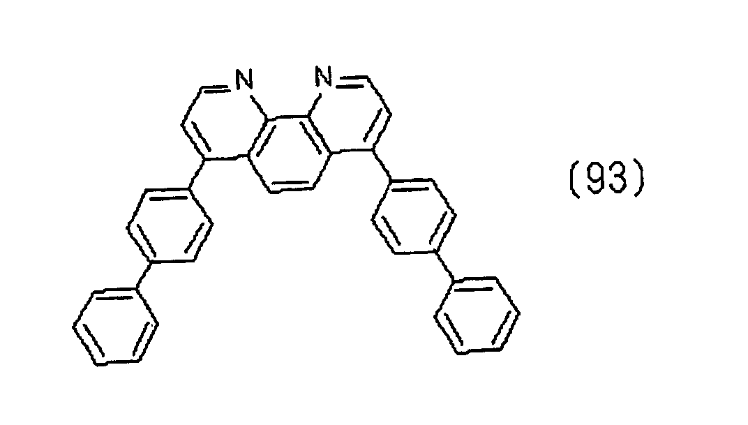
- organic material having the electron transportability usable for the electron transport layer 6 can also be selected from phenanthroline derivatives represented by the following formulae (88) to (96):
- the phosphorescent organic guest material for use in light emitting layer 4 can also be selected from the compounds shown by the structural formulae (2) to (6), for example, materials shown by the following formulae (97) to (106):
- Plural organic EL devices were manufactured as samples specifically and light emitting characteristics thereof were evaluated.
- CuPc copper phthalocyanine
- NPB hole transport layer
- Alq3 the electron transport layer.
- thin films of the respective materials were stacked successively on a glass substrate formed with an anode made of ITO with a film thickness of 1100 ⁇ by vacuum vapor deposition at a vacuum degree of 5.0 ⁇ 10 -6 Torr.
- CuPc was deposited as a film to 250 ⁇ thickness on a ITO cathode at a vapor deposition rate of 3 ⁇ /sec, to form a hole injection layer.
- NPB was deposited as a film to 550 ⁇ thickness on a CuPc hole injection layer at a vapor deposition rate of 3 ⁇ /sec to form a hole transport layer.
- an organic host material of the structural formula (1) and an organic guest material XT emitting red phosphorous among the compounds shown by the structural formula (6) were co-deposited from different vapor deposition sources to 475 ⁇ thickness to form a light emitting layer.
- the concentration of the organic guest material XT in the light emitting layer was 7 wt%.
- Alq3 was vapor deposited to 300 ⁇ thickness at a vapor deposition rate of 3 ⁇ /sec to form an electron transport layer.
- lithium oxide Li 2 O
- Al aluminum
- Example 2 As a comparative example, a device of comparative example identical with that of Example 1 was also manufactured except for using BAlq for the organic host material in the mixed light emitting layer.
- Fig. 1 shows change of degradation of luminance and driving voltage when Example 1 and Comparative Example were driven continuously at a constant current of 5.5 mA/cm 2 from the initial luminance of 340 cd/m 2 .
- the luminance half-decay period was extended compared with the comparative example and the luminance life was excellent.
- Change of the driving voltage (increase) is one of parameters showing the degradation of the material along with continuous driving.
- Table 1 and Table 2 show the change of chromaticity, luminance and voltage relative to lapse of time in a case of driving the devices of Example 1 and Comparative Example at 5.5 mA/cm 2 respectively.
- Driving voltage (V) CIEx CIEy 0 0.678 0.321 337 9.20 63 0.677 0.323 269 6.93 159 0.576 0.386 66 6.51 324 0.528 0.416 63 6.79 500 0.525 0.423 65 6.92
- the luminance was lowered by 80% relative to the initial value at lapse of 160 hrs at 100°C, Further, change of chromaticity was observed and the emission color changed from red to yellow.
- the glass transition temperature Tg of the structural formula (1) of the organic host material is 113°C and the glass transition temperature Tg of BAlq is 99°C. It is considered that since the organic host material of the light emitting layer of the example had higher Tg than that of the comparative example and the physical and electrical characteristics of the thin film in the organic EL device were stable, the degradation of luminance during continuous driving was suppressed and the driving life was improved compared with the device of the comparative example.
- the organic host material shown by the structural formula (1) had a ligand of longer conjugation system compared with BAlq used in the comparative example, it is excellent in the electron transportability.
- the organic EL device using the organic host material shown by the structural material (1) as the light emitting layer had more preferred current luminance characteristics than those of the device using BAlq as the light emitting layer and suffered from less lowering of efficiency, particularly, in a higher luminance region exceeding 300 cd/m 2 .
- a devices was manufactured quite in the same manner as Example 1 except for using 2,3,7,8,12,13,17,18-octaethyl-21H,23H-porphinePlatinum (II) (so-called PtOEP), instead of the organic guest material XT, as the phosphorescent organic guest material under the identical condition.
- II 2,3,7,8,12,13,17,18-octaethyl-21H,23H-porphinePlatinum
- Table 3 shows the light emitting characteristics during continuous driving at a constant current of 2.5 mA/cm 2
- Fig. 5 shows voltage-luminance characteristics
- Fig. 6 shows current-luminance characteristics, respectively.
- the device of Example 2 using the material of the structural formula (1) of the invention for the host material in the light emitting layer had more satisfactory voltage-luminance characteristics and current characteristics compared with the device of the comparative example. That is, the device of high efficiency and low driving voltage could be obtained by using the material shown by the structural formula (1) as the host material of the light emitting layer.
- Fig. 7 shows the change of degradation of luminance and driving voltage during continuous driving at a constant current of 7.5 mA/cm 2 .
- both the device of Example 2 and the device of the comparative example maintained 95% or more of the initial luminance.
- For the driving voltage it increased by 6.4% at the lapse of time of 300 hrs in the device of the comparative example, whereas it was suppressed to 3.5% in the device of Example 2.
- the organic host material of an aluminum chelate complex of the specified structure shown by the structural formula (1) is used as the main ingredient of the light emitting layer in the organic EL device having the light emitting layer using the phosphorescent material for the organic guest material, it is excellent in heat resistance and can attain a long driving life while maintaining favorable light emitting characteristics.
Landscapes
- Chemical & Material Sciences (AREA)
- Engineering & Computer Science (AREA)
- Materials Engineering (AREA)
- Organic Chemistry (AREA)
- Inorganic Chemistry (AREA)
- Electroluminescent Light Sources (AREA)
Abstract
Description


| Lapse of time (hours) | Chromaticity diagram | Luminance | Driving voltage | |
| ClEx | CIEy | (cd/m2) | (V) | |
| 0 | 0.676 | 0.321 | 326 | 8.41 |
| 63 | 0.676 | 0.323 | 322 | 7.70 |
| 159 | 0.673 | 0.324 | 292 | 7.24 |
| 324 | 0.672 | 0.325 | 239 | 7.09 |
| 500 | 0.667 | 0.328 | 197 | 6.86 |
| Lapse of time (hours) | Chromaticity diagram | Luminance (cd/m2) | Driving voltage (V) | |
| | CIEy | |||
| 0 | 0.678 | 0.321 | 337 | 9.20 |
| 63 | 0.677 | 0.323 | 269 | 6.93 |
| 159 | 0.576 | 0.386 | 66 | 6.51 |
| 324 | 0.528 | 0.416 | 63 | 6.79 |
| 500 | 0.525 | 0.423 | 65 | 6.92 |
| Chromaticity diagram | Luminance (cd/m2) (cd/m2) | Quantum efficiency (%) | Driving voltage (V) | ||
| CIEx | CIEy | ||||
| Example 2 | 0.695 | 0.294 | 43 | 5.35 | 8.85 |
| Comp. Example | 0.709 | 0.283 | 38 | 4.89 | 9.66 |
Claims (14)
- An organic electroluminescence device comprising:an anode; a hole transport layer comprising an organiccompound; a light emitting layer having an organic compound; an electron transport layer having an organic compound; anda cathode which are stacked, characterized in that the light emitting layer includes an organic host material represented by the following structural formula (1):
 and a phosphorescent organic guest material.
 - An organic electroluminescence device according to claim 1, wherein a hole injection layer is provided between the anode and the hole transportation.
- An organic electroluminescence device according to claim 1 or claim 2, wherein an electron injection layer is provided between the cathode and the electron transport layer.
- An organic electroluminescence device according to any one of claims 1 to 3, wherein the phosphorescent organic guest material comprises a porphyrin compound represented by the following structural formula (2):(in the structural formula (2), Q represents -N= or -C(R)=, M represents a metal, a metal oxide, or a metal halide, R represents hydrogen, alkyl, aralkyl, aryl or alkalyl, or a halogenated substituent thereof, T1 and T2 each represents hydrogen or alkyl, or jointly represent a completed unsaturated six-membered ring including a halogen substituent, the six-membered ring is formed of carbon, sulfur and nitrogen ring atoms, and the alkyl moiety contains 1 to 6 carbon atoms).

- An organic electroluminescence device according to claim 4, wherein M in the phosphorescent organic guest material is platinum.
- An organic electroluminescence device according to any one of claims 1 to 3, wherein the phosphorescent organic guest material comprises a compound represented by the following structural formula (3):(in the structural formula (3), M represents a metal, R1 to R8 each independently includes a hydrogen atom, alkyl group, oxy group, amino group or a hydrocarbon group having at least one carbon atom in the substituent, the number of carbon atoms is 1 to 10 in each of the hydrocarbon moieties, further, R1 to R8 can be selected independently from cyano, halogen, and α-haloalkyl, α-haloalkoxy, amide, sulfonyl, carbonyl, carbonyloxy and oxycarbonyl substituents containing 10 or less carbon atoms, and further, R1 together with R2, R2 together with R3, R3 together with R4, R5 together with R6, R6 together with R7, or R7 together with R8 can form a condensed benzo ring).

- An organic electroluminescence device according to claim 6, wherein M in the phosphorescent organic guest material is iridium.
- An organic electroluminescence device according to any one of claims 1 to 3, wherein the phosphorescent organic guest material comprises a compound represented by the following structural formula (4):(in the structural formula (4), M represents a metal, R1 to R6 each independently includes a hydrogen atom, alkyl group, oxy group, amino group or a hydrocarbon group having at least one carbon atom in the substituent, the number of carbon atoms is 1 to 10 in each of the hydrocarbon moieties, further, R1 to R6 can be selected independently from cyano, halogen, and α-haloalkyl, α-haloalkoxy, amide, sulfonyl, carbonyl, carbonyloxy and oxycarbonyl substituents containing 10 or less carbon atoms and, further, R1 together with R2, R3 together with R4, R4 together with R5, or R5 together with R6 can form a condensed benzo ring).

- An organic electroluminescence device according to claim 8, wherein M in the phosphorescent organic guest material is iridium.
- An organic electroluminescence device according to any one of claims 1 to 3, wherein the phosphorescent organic guest material comprises a compound represented by the following structural formula (5):(in the structural formula (5), M represents a metal, X1 and X2 each independently represents an oxygen atom or a sulfur atom, R1 to R11 each independently includes a hydrogen atom, alkyl group, oxy group, amino group, or a hydrocarbon group having at least one carbon atom in the substituent, the number of carbon atoms is 1 to 10 in each of the hydrocarbon moieties, further, R1 to R11 can be selected independently from cyano, halogen, and α-haloalkyl, α-haloalkoxy, amide, sulfonyl, carbonyl, carbonyloxy and oxycarbonyl substituents containing 10 or less carbon atoms and, further, R1 together with R2, R2 together with R3, R3 together with R4, R5 together with R6, R6 together with R7, R7 together with R8, or R8 together with R9 can form a condensed benzo ring).

- An organic electroluminescence device according to claim 10, wherein M for the phosphorescent organic guest material is iridium.
- An organic electroluminescence device according to any one of claims 1 to 3, where in phosphorescent organic guest material comprises a compound represented by the following structural formula (6):(in the structural formula (6), M represents a metal, X1 and X2 each independently represents an oxygen atom or a sulfur atom, R1 to R9 each independently includes a hydrogen atom, alkyl group, oxy group, amino group or a hydrocarbon group having at least one carbon atom in the substituent, the number of carbon atoms is 1 to 10 in each of the hydrocarbon moieties, further. R1 to R9 can be selected independently from cyano, halogen, and α-haloalkyl, α-haloalkoxy, amide, sulfonyl, carbonyl, carbonyloxy and oxycarbonyl substituents containing 10 or less of carbon atoms and, further, R1 together with R2, R3 together with R4, R4 together with R5, R5 together with R6, R7 together with R8, R8 together with R9, R9 together with R10, or R10 together with R11 can form a condensed benzo ring).

- An organic electroluminescence device according to claim 12, wherein M in the phosphorescent organic guest material is iridium.
- A material for an organic electric field light emitting device material which is a compound represented by the following structural material (1):

Applications Claiming Priority (3)
| Application Number | Priority Date | Filing Date | Title |
|---|---|---|---|
| JP2002096908 | 2002-03-29 | ||
| JP2002096908 | 2002-03-29 | ||
| PCT/JP2003/003776 WO2003083009A1 (en) | 2002-03-29 | 2003-03-27 | Organic electroluminescence element |
Publications (3)
| Publication Number | Publication Date |
|---|---|
| EP1493797A1 true EP1493797A1 (en) | 2005-01-05 |
| EP1493797A4 EP1493797A4 (en) | 2009-01-14 |
| EP1493797B1 EP1493797B1 (en) | 2012-11-14 |
Family
ID=28671852
Family Applications (1)
| Application Number | Title | Priority Date | Filing Date |
|---|---|---|---|
| EP03715461A Expired - Lifetime EP1493797B1 (en) | 2002-03-29 | 2003-03-27 | Organic electroluminescence element |
Country Status (7)
| Country | Link |
|---|---|
| US (1) | US7781072B2 (en) |
| EP (1) | EP1493797B1 (en) |
| JP (1) | JP4251553B2 (en) |
| KR (1) | KR100673052B1 (en) |
| CN (2) | CN1643109A (en) |
| AU (1) | AU2003227239A1 (en) |
| WO (1) | WO2003083009A1 (en) |
Cited By (6)
| Publication number | Priority date | Publication date | Assignee | Title |
|---|---|---|---|---|
| WO2005076380A3 (en) * | 2004-02-03 | 2005-11-03 | Universal Display Corp | Oleds utilizing multidentate ligand systems |
| WO2006033857A1 (en) * | 2004-09-20 | 2006-03-30 | Eastman Kodak Company | Organic electroluminescent devices and composition |
| WO2006119800A1 (en) * | 2005-05-09 | 2006-11-16 | Technische Universität Braunschweig | Light emitting compound for electroluminescent applications |
| US7709105B2 (en) | 2005-12-14 | 2010-05-04 | Global Oled Technology Llc | Electroluminescent host material |
| US7807275B2 (en) | 2005-04-21 | 2010-10-05 | Universal Display Corporation | Non-blocked phosphorescent OLEDs |
| WO2016116485A1 (en) * | 2015-01-20 | 2016-07-28 | Cynora Gmbh | Azoles for use in optoelectronic components |
Families Citing this family (12)
| Publication number | Priority date | Publication date | Assignee | Title |
|---|---|---|---|---|
| JP4011325B2 (en) * | 2001-10-31 | 2007-11-21 | パイオニア株式会社 | Organic electroluminescence device |
| TWI390006B (en) * | 2003-08-07 | 2013-03-21 | Nippon Steel Chemical Co | Organic EL materials with aluminum clamps |
| JP4145280B2 (en) * | 2004-02-27 | 2008-09-03 | 富士フイルム株式会社 | Light emitting element |
| CN100591184C (en) * | 2004-03-15 | 2010-02-17 | 新日铁化学株式会社 | Organic electroluminescent element |
| JP4749744B2 (en) * | 2004-03-31 | 2011-08-17 | 富士フイルム株式会社 | Organic electroluminescence device |
| US7579090B2 (en) * | 2004-09-20 | 2009-08-25 | Eastman Kodak Company | Organic element for electroluminescent devices |
| JP4813032B2 (en) * | 2004-09-21 | 2011-11-09 | 富士フイルム株式会社 | Organic electroluminescence device |
| KR100970713B1 (en) * | 2007-12-31 | 2010-07-16 | 다우어드밴스드디스플레이머티리얼 유한회사 | Electroluminescent device Green using the electroluminescent compounds |
| DE112010003859B4 (en) | 2009-09-30 | 2020-09-10 | Mitsubishi Electric Corp. | Lundell-type rotary motor |
| KR101294620B1 (en) * | 2010-06-07 | 2013-08-07 | 롬엔드하스전자재료코리아유한회사 | Electroluminescent device Green using the electroluminescent compounds |
| WO2013171872A1 (en) * | 2012-05-17 | 2013-11-21 | パイオニア株式会社 | Organic el light-emitting panel and light-emitting device |
| CN107557000B (en) * | 2017-11-14 | 2020-04-24 | 浙江工业大学 | Class A3B-type asymmetric metal platinum porphyrin organic luminescent material and application thereof |
Citations (3)
| Publication number | Priority date | Publication date | Assignee | Title |
|---|---|---|---|---|
| US5141671A (en) * | 1991-08-01 | 1992-08-25 | Eastman Kodak Company | Mixed ligand 8-quinolinolato aluminum chelate luminophors |
| US5150006A (en) * | 1991-08-01 | 1992-09-22 | Eastman Kodak Company | Blue emitting internal junction organic electroluminescent device (II) |
| EP0726304A2 (en) * | 1995-02-13 | 1996-08-14 | Motorola, Inc. | Organometallic complexes with built-in fluorescent dyes for use in light emitting devices |
Family Cites Families (10)
| Publication number | Priority date | Publication date | Assignee | Title |
|---|---|---|---|---|
| DE69305262T2 (en) | 1992-07-13 | 1997-04-30 | Eastman Kodak Co | Internal transition organic electroluminescent device with a new composition |
| JP3758694B2 (en) | 1994-10-13 | 2006-03-22 | 三星エスディアイ株式会社 | Organic thin film EL device |
| JPH10233284A (en) | 1997-02-19 | 1998-09-02 | Oki Electric Ind Co Ltd | Organic el element |
| US6303238B1 (en) * | 1997-12-01 | 2001-10-16 | The Trustees Of Princeton University | OLEDs doped with phosphorescent compounds |
| JP4224921B2 (en) | 2000-03-27 | 2009-02-18 | 東洋インキ製造株式会社 | Material for organic electroluminescence device and organic electroluminescence device using the same |
| JP2001326080A (en) | 2000-05-18 | 2001-11-22 | Tohoku Pioneer Corp | Organic electroluminescent element |
| TW536836B (en) * | 2000-05-22 | 2003-06-11 | Semiconductor Energy Lab | Light emitting device and electrical appliance |
| US6791258B2 (en) * | 2001-06-21 | 2004-09-14 | 3M Innovative Properties Company | Organic light emitting full color display panel |
| JP4011325B2 (en) * | 2001-10-31 | 2007-11-21 | パイオニア株式会社 | Organic electroluminescence device |
| TWI390006B (en) * | 2003-08-07 | 2013-03-21 | Nippon Steel Chemical Co | Organic EL materials with aluminum clamps |
-
2003
- 2003-03-27 JP JP2003580447A patent/JP4251553B2/en not_active Expired - Fee Related
- 2003-03-27 EP EP03715461A patent/EP1493797B1/en not_active Expired - Lifetime
- 2003-03-27 CN CNA038073943A patent/CN1643109A/en active Pending
- 2003-03-27 US US10/509,390 patent/US7781072B2/en active Active
- 2003-03-27 WO PCT/JP2003/003776 patent/WO2003083009A1/en active Application Filing
- 2003-03-27 AU AU2003227239A patent/AU2003227239A1/en not_active Abandoned
- 2003-03-27 CN CN201210243327.2A patent/CN102796513B/en not_active Expired - Lifetime
- 2003-03-27 KR KR1020047015428A patent/KR100673052B1/en active IP Right Grant
Patent Citations (3)
| Publication number | Priority date | Publication date | Assignee | Title |
|---|---|---|---|---|
| US5141671A (en) * | 1991-08-01 | 1992-08-25 | Eastman Kodak Company | Mixed ligand 8-quinolinolato aluminum chelate luminophors |
| US5150006A (en) * | 1991-08-01 | 1992-09-22 | Eastman Kodak Company | Blue emitting internal junction organic electroluminescent device (II) |
| EP0726304A2 (en) * | 1995-02-13 | 1996-08-14 | Motorola, Inc. | Organometallic complexes with built-in fluorescent dyes for use in light emitting devices |
Non-Patent Citations (1)
| Title |
|---|
| See also references of WO03083009A1 * |
Cited By (10)
| Publication number | Priority date | Publication date | Assignee | Title |
|---|---|---|---|---|
| WO2005076380A3 (en) * | 2004-02-03 | 2005-11-03 | Universal Display Corp | Oleds utilizing multidentate ligand systems |
| WO2006033857A1 (en) * | 2004-09-20 | 2006-03-30 | Eastman Kodak Company | Organic electroluminescent devices and composition |
| US7807275B2 (en) | 2005-04-21 | 2010-10-05 | Universal Display Corporation | Non-blocked phosphorescent OLEDs |
| US8685540B2 (en) | 2005-04-21 | 2014-04-01 | Universal Display Corporation | Non-blocked phosphorescent OLEDs |
| US10593900B2 (en) | 2005-04-21 | 2020-03-17 | Universal Display Corporation | Non-blocked phosphorescent OLEDs |
| US10916721B2 (en) | 2005-04-21 | 2021-02-09 | Universal Display Corporation | Non-blocked phosphorescent OLEDs |
| US11594697B2 (en) | 2005-04-21 | 2023-02-28 | Universal Display Corporation | Non-blocked phosphorescent OLEDs |
| WO2006119800A1 (en) * | 2005-05-09 | 2006-11-16 | Technische Universität Braunschweig | Light emitting compound for electroluminescent applications |
| US7709105B2 (en) | 2005-12-14 | 2010-05-04 | Global Oled Technology Llc | Electroluminescent host material |
| WO2016116485A1 (en) * | 2015-01-20 | 2016-07-28 | Cynora Gmbh | Azoles for use in optoelectronic components |
Also Published As
| Publication number | Publication date |
|---|---|
| EP1493797A4 (en) | 2009-01-14 |
| US7781072B2 (en) | 2010-08-24 |
| CN102796513A (en) | 2012-11-28 |
| CN1643109A (en) | 2005-07-20 |
| KR100673052B1 (en) | 2007-01-22 |
| JPWO2003083009A1 (en) | 2005-08-04 |
| JP4251553B2 (en) | 2009-04-08 |
| AU2003227239A1 (en) | 2003-10-13 |
| EP1493797B1 (en) | 2012-11-14 |
| WO2003083009A1 (en) | 2003-10-09 |
| KR20040111447A (en) | 2004-12-31 |
| CN102796513B (en) | 2015-07-08 |
| US20050233164A1 (en) | 2005-10-20 |
Similar Documents
| Publication | Publication Date | Title |
|---|---|---|
| JP6025959B2 (en) | 2-Azatriphenylene materials for organic light-emitting diodes | |
| JP4011325B2 (en) | Organic electroluminescence device | |
| JP4037033B2 (en) | Organic electroluminescence device | |
| JP5746269B2 (en) | Organic light-emitting device having phosphorescent-sensitized fluorescent light-emitting layer | |
| KR101932823B1 (en) | Improved oled stability via doped hole transport layer | |
| EP1493797B1 (en) | Organic electroluminescence element | |
| EP2097938A2 (en) | Long lifetime phosphorescent organic light emitting device (oled) structures | |
| EP1391495B1 (en) | Organic electroluminescence element | |
| US20030108770A1 (en) | Organic electroluminescent device | |
| KR101201174B1 (en) | Organic electroluminescent element | |
| KR100611850B1 (en) | Phosphorescent iridium complex and organic electroluminescent device comprising same | |
| EP1809077A2 (en) | Organic electroluminescent element | |
| KR100649283B1 (en) | Phosphorescent host compound and organic electroluminescent device comprising same | |
| KR100687958B1 (en) | Iridium complex and organic electroluminescent device comprising same | |
| KR100611852B1 (en) | Phosphorescent red-emitting iridium complex and organic electroluminescent device comprising same | |
| KR100696005B1 (en) | 1-naphthylisoquinoline-containing phosphorescent red-emitting iridium complex and organic electroluminescent device comprising same | |
| JP2007150338A (en) | Organic electroluminescent element | |
| KR20190028878A (en) | Arylamine derivative and organic electro luminescent device including the same | |
| KR20070016298A (en) | Organin Host Materials And Organic Electroluminescent Device using this material | |
| KR20060120984A (en) | Phosphorescent host materials with aluminium complex containing 9-phenanthrol and organic electroluminescent device using this material | |
| KR20060105150A (en) | Organic electroluminescent device having long life time |
Legal Events
| Date | Code | Title | Description |
|---|---|---|---|
| PUAI | Public reference made under article 153(3) epc to a published international application that has entered the european phase |
Free format text: ORIGINAL CODE: 0009012 |
|
| 17P | Request for examination filed |
Effective date: 20040924 |
|
| AK | Designated contracting states |
Kind code of ref document: A1 Designated state(s): AT BE BG CH CY CZ DE DK EE ES FI FR GB GR HU IE IT LI LU MC NL PT RO SE SI SK TR |
|
| AX | Request for extension of the european patent |
Extension state: AL LT LV MK |
|
| A4 | Supplementary search report drawn up and despatched |
Effective date: 20081216 |
|
| RAP1 | Party data changed (applicant data changed or rights of an application transferred) |
Owner name: PIONEER CORPORATION Owner name: NIPPON STEEL CHEMICAL CO., LTD. |
|
| 17Q | First examination report despatched |
Effective date: 20110111 |
|
| REG | Reference to a national code |
Ref country code: DE Ref legal event code: R079 Ref document number: 60342583 Country of ref document: DE Free format text: PREVIOUS MAIN CLASS: C09K0011060000 Ipc: H01L0051000000 |
|
| GRAP | Despatch of communication of intention to grant a patent |
Free format text: ORIGINAL CODE: EPIDOSNIGR1 |
|
| RIC1 | Information provided on ipc code assigned before grant |
Ipc: C09K 11/06 20060101ALI20120410BHEP Ipc: H01L 51/00 20060101AFI20120410BHEP |
|
| GRAS | Grant fee paid |
Free format text: ORIGINAL CODE: EPIDOSNIGR3 |
|
| GRAA | (expected) grant |
Free format text: ORIGINAL CODE: 0009210 |
|
| AK | Designated contracting states |
Kind code of ref document: B1 Designated state(s): DE FR GB NL |
|
| REG | Reference to a national code |
Ref country code: GB Ref legal event code: FG4D |
|
| REG | Reference to a national code |
Ref country code: DE Ref legal event code: R096 Ref document number: 60342583 Country of ref document: DE Effective date: 20130110 |
|
| REG | Reference to a national code |
Ref country code: NL Ref legal event code: VDEP Effective date: 20121114 |
|
| RAP2 | Party data changed (patent owner data changed or rights of a patent transferred) |
Owner name: NIPPON STEEL & SUMIKIN CHEMICAL CO., LTD. Owner name: PIONEER CORPORATION |
|
| REG | Reference to a national code |
Ref country code: DE Ref legal event code: R082 Ref document number: 60342583 Country of ref document: DE Representative=s name: MANITZ, FINSTERWALD & PARTNER GBR, DE |
|
| PG25 | Lapsed in a contracting state [announced via postgrant information from national office to epo] |
Ref country code: NL Free format text: LAPSE BECAUSE OF FAILURE TO SUBMIT A TRANSLATION OF THE DESCRIPTION OR TO PAY THE FEE WITHIN THE PRESCRIBED TIME-LIMIT Effective date: 20121114 |
|
| PLBE | No opposition filed within time limit |
Free format text: ORIGINAL CODE: 0009261 |
|
| STAA | Information on the status of an ep patent application or granted ep patent |
Free format text: STATUS: NO OPPOSITION FILED WITHIN TIME LIMIT |
|
| REG | Reference to a national code |
Ref country code: DE Ref legal event code: R081 Ref document number: 60342583 Country of ref document: DE Owner name: PIONEER CORP., JP Free format text: FORMER OWNER: PIONEER CORP., NIPPON STEEL CHEMICAL CO., LTD., , JP Effective date: 20121031 Ref country code: DE Ref legal event code: R082 Ref document number: 60342583 Country of ref document: DE Representative=s name: MANITZ, FINSTERWALD & PARTNER GBR, DE Effective date: 20130827 Ref country code: DE Ref legal event code: R081 Ref document number: 60342583 Country of ref document: DE Owner name: NIPPON STEEL & SUMIKIN CHEMICAL CO., LTD., JP Free format text: FORMER OWNER: PIONEER CORP., NIPPON STEEL CHEMICAL CO., LTD., , JP Effective date: 20121031 Ref country code: DE Ref legal event code: R081 Ref document number: 60342583 Country of ref document: DE Owner name: NIPPON STEEL & SUMIKIN CHEMICAL CO., LTD., JP Free format text: FORMER OWNER: PIONEER CORP., NIPPON STEEL CHEMICAL CO., LTD., , JP Effective date: 20130827 Ref country code: DE Ref legal event code: R081 Ref document number: 60342583 Country of ref document: DE Owner name: PIONEER CORP., JP Free format text: FORMER OWNER: PIONEER CORP., NIPPON STEEL CHEMICAL CO., LTD., , JP Effective date: 20130827 Ref country code: DE Ref legal event code: R081 Ref document number: 60342583 Country of ref document: DE Owner name: PIONEER CORP., JP Free format text: FORMER OWNERS: PIONEER CORP., TOKIO/TOKYO, JP; NIPPON STEEL CHEMICAL CO., LTD., TOKIO/TOKYO, JP Effective date: 20130827 Ref country code: DE Ref legal event code: R081 Ref document number: 60342583 Country of ref document: DE Owner name: PIONEER CORP., JP Free format text: FORMER OWNERS: PIONEER CORP., TOKIO/TOKYO, JP; NIPPON STEEL CHEMICAL CO., LTD., TOKIO/TOKYO, JP Effective date: 20121031 Ref country code: DE Ref legal event code: R081 Ref document number: 60342583 Country of ref document: DE Owner name: NIPPON STEEL & SUMIKIN CHEMICAL CO., LTD., JP Free format text: FORMER OWNERS: PIONEER CORP., TOKIO/TOKYO, JP; NIPPON STEEL CHEMICAL CO., LTD., TOKIO/TOKYO, JP Effective date: 20130827 Ref country code: DE Ref legal event code: R081 Ref document number: 60342583 Country of ref document: DE Owner name: NIPPON STEEL & SUMIKIN CHEMICAL CO., LTD., JP Free format text: FORMER OWNERS: PIONEER CORP., TOKIO/TOKYO, JP; NIPPON STEEL CHEMICAL CO., LTD., TOKIO/TOKYO, JP Effective date: 20121031 Ref country code: DE Ref legal event code: R082 Ref document number: 60342583 Country of ref document: DE Representative=s name: MANITZ FINSTERWALD PATENTANWAELTE PARTMBB, DE Effective date: 20130827 |
|
| 26N | No opposition filed |
Effective date: 20130815 |
|
| REG | Reference to a national code |
Ref country code: DE Ref legal event code: R097 Ref document number: 60342583 Country of ref document: DE Effective date: 20130815 |
|
| REG | Reference to a national code |
Ref country code: FR Ref legal event code: ST Effective date: 20131129 |
|
| PG25 | Lapsed in a contracting state [announced via postgrant information from national office to epo] |
Ref country code: FR Free format text: LAPSE BECAUSE OF NON-PAYMENT OF DUE FEES Effective date: 20130402 |
|
| PGFP | Annual fee paid to national office [announced via postgrant information from national office to epo] |
Ref country code: GB Payment date: 20150325 Year of fee payment: 13 |
|
| GBPC | Gb: european patent ceased through non-payment of renewal fee |
Effective date: 20160327 |
|
| PG25 | Lapsed in a contracting state [announced via postgrant information from national office to epo] |
Ref country code: GB Free format text: LAPSE BECAUSE OF NON-PAYMENT OF DUE FEES Effective date: 20160327 |
|
| REG | Reference to a national code |
Ref country code: DE Ref legal event code: R081 Ref document number: 60342583 Country of ref document: DE Owner name: PIONEER CORP., JP Free format text: FORMER OWNERS: NIPPON STEEL & SUMIKIN CHEMICAL CO., LTD., TOKYO, JP; PIONEER CORP., TOKIO/TOKYO, JP Ref country code: DE Ref legal event code: R081 Ref document number: 60342583 Country of ref document: DE Owner name: NIPPON STEEL CHEMICAL & MATERIAL CO., LTD., JP Free format text: FORMER OWNERS: NIPPON STEEL & SUMIKIN CHEMICAL CO., LTD., TOKYO, JP; PIONEER CORP., TOKIO/TOKYO, JP |
|
| PGFP | Annual fee paid to national office [announced via postgrant information from national office to epo] |
Ref country code: DE Payment date: 20220203 Year of fee payment: 20 |
|
| REG | Reference to a national code |
Ref country code: DE Ref legal event code: R079 Ref document number: 60342583 Country of ref document: DE Free format text: PREVIOUS MAIN CLASS: H01L0051000000 Ipc: H10K0099000000 |
|
| REG | Reference to a national code |
Ref country code: DE Ref legal event code: R071 Ref document number: 60342583 Country of ref document: DE |
|
| P01 | Opt-out of the competence of the unified patent court (upc) registered |
Effective date: 20230510 |