EP1450418A2 - Area light emitting device, method for manufacturing the same, and liquid crystal display unit - Google Patents
Area light emitting device, method for manufacturing the same, and liquid crystal display unit Download PDFInfo
- Publication number
- EP1450418A2 EP1450418A2 EP04003656A EP04003656A EP1450418A2 EP 1450418 A2 EP1450418 A2 EP 1450418A2 EP 04003656 A EP04003656 A EP 04003656A EP 04003656 A EP04003656 A EP 04003656A EP 1450418 A2 EP1450418 A2 EP 1450418A2
- Authority
- EP
- European Patent Office
- Prior art keywords
- transparent substrate
- exit surface
- light emitting
- emitting device
- light exit
- Prior art date
- Legal status (The legal status is an assumption and is not a legal conclusion. Google has not performed a legal analysis and makes no representation as to the accuracy of the status listed.)
- Withdrawn
Links
Images

Classifications
-
- A—HUMAN NECESSITIES
- A61—MEDICAL OR VETERINARY SCIENCE; HYGIENE
- A61H—PHYSICAL THERAPY APPARATUS, e.g. DEVICES FOR LOCATING OR STIMULATING REFLEX POINTS IN THE BODY; ARTIFICIAL RESPIRATION; MASSAGE; BATHING DEVICES FOR SPECIAL THERAPEUTIC OR HYGIENIC PURPOSES OR SPECIFIC PARTS OF THE BODY
- A61H23/00—Percussion or vibration massage, e.g. using supersonic vibration; Suction-vibration massage; Massage with moving diaphragms
- A61H23/02—Percussion or vibration massage, e.g. using supersonic vibration; Suction-vibration massage; Massage with moving diaphragms with electric or magnetic drive
-
- G—PHYSICS
- G02—OPTICS
- G02F—OPTICAL DEVICES OR ARRANGEMENTS FOR THE CONTROL OF LIGHT BY MODIFICATION OF THE OPTICAL PROPERTIES OF THE MEDIA OF THE ELEMENTS INVOLVED THEREIN; NON-LINEAR OPTICS; FREQUENCY-CHANGING OF LIGHT; OPTICAL LOGIC ELEMENTS; OPTICAL ANALOGUE/DIGITAL CONVERTERS
- G02F1/00—Devices or arrangements for the control of the intensity, colour, phase, polarisation or direction of light arriving from an independent light source, e.g. switching, gating or modulating; Non-linear optics
- G02F1/01—Devices or arrangements for the control of the intensity, colour, phase, polarisation or direction of light arriving from an independent light source, e.g. switching, gating or modulating; Non-linear optics for the control of the intensity, phase, polarisation or colour
- G02F1/13—Devices or arrangements for the control of the intensity, colour, phase, polarisation or direction of light arriving from an independent light source, e.g. switching, gating or modulating; Non-linear optics for the control of the intensity, phase, polarisation or colour based on liquid crystals, e.g. single liquid crystal display cells
- G02F1/133—Constructional arrangements; Operation of liquid crystal cells; Circuit arrangements
- G02F1/1333—Constructional arrangements; Manufacturing methods
- G02F1/1335—Structural association of cells with optical devices, e.g. polarisers or reflectors
- G02F1/1336—Illuminating devices
- G02F1/133602—Direct backlight
- G02F1/133603—Direct backlight with LEDs
-
- A—HUMAN NECESSITIES
- A61—MEDICAL OR VETERINARY SCIENCE; HYGIENE
- A61H—PHYSICAL THERAPY APPARATUS, e.g. DEVICES FOR LOCATING OR STIMULATING REFLEX POINTS IN THE BODY; ARTIFICIAL RESPIRATION; MASSAGE; BATHING DEVICES FOR SPECIAL THERAPEUTIC OR HYGIENIC PURPOSES OR SPECIFIC PARTS OF THE BODY
- A61H23/00—Percussion or vibration massage, e.g. using supersonic vibration; Suction-vibration massage; Massage with moving diaphragms
- A61H23/006—Percussion or tapping massage
-
- A—HUMAN NECESSITIES
- A61—MEDICAL OR VETERINARY SCIENCE; HYGIENE
- A61H—PHYSICAL THERAPY APPARATUS, e.g. DEVICES FOR LOCATING OR STIMULATING REFLEX POINTS IN THE BODY; ARTIFICIAL RESPIRATION; MASSAGE; BATHING DEVICES FOR SPECIAL THERAPEUTIC OR HYGIENIC PURPOSES OR SPECIFIC PARTS OF THE BODY
- A61H39/00—Devices for locating or stimulating specific reflex points of the body for physical therapy, e.g. acupuncture
- A61H39/04—Devices for pressing such points, e.g. Shiatsu or Acupressure
-
- H—ELECTRICITY
- H10—SEMICONDUCTOR DEVICES; ELECTRIC SOLID-STATE DEVICES NOT OTHERWISE PROVIDED FOR
- H10K—ORGANIC ELECTRIC SOLID-STATE DEVICES
- H10K50/00—Organic light-emitting devices
- H10K50/80—Constructional details
- H10K50/85—Arrangements for extracting light from the devices
-
- A—HUMAN NECESSITIES
- A61—MEDICAL OR VETERINARY SCIENCE; HYGIENE
- A61H—PHYSICAL THERAPY APPARATUS, e.g. DEVICES FOR LOCATING OR STIMULATING REFLEX POINTS IN THE BODY; ARTIFICIAL RESPIRATION; MASSAGE; BATHING DEVICES FOR SPECIAL THERAPEUTIC OR HYGIENIC PURPOSES OR SPECIFIC PARTS OF THE BODY
- A61H2205/00—Devices for specific parts of the body
- A61H2205/02—Head
-
- H—ELECTRICITY
- H10—SEMICONDUCTOR DEVICES; ELECTRIC SOLID-STATE DEVICES NOT OTHERWISE PROVIDED FOR
- H10K—ORGANIC ELECTRIC SOLID-STATE DEVICES
- H10K50/00—Organic light-emitting devices
- H10K50/80—Constructional details
Definitions
- the present invention relates to an area light emitting device emitting light through an area, a method for manufacturing such a light emitting device, and a liquid crystal display unit having such a light emitting device.
- a typical area light emitting device has an area light emitting element emitting light through an area. Light from such an area light emitting element is emitted through a flat substrate. In this case, only 20 to 25% of light from the light emitting element exits the light emitting device. That is, the light emitting device is unable to efficiently emit light emitted from the light emitting element. This is because a great proportion of light from the light emitting element is reflected on an interface between the flat substrate and air.
- a plano-convex lens is formed in each section of a substrate that corresponds to a pixel, thereby increasing the proportion of light that exits the organic EL device.
- light scatterers which are asperities formed by etching a transparent film, are provided on a substrate to increase the proportion of light that exits the light emitting device.
- an objective of the present invention to provide a novel area light emitting device that is capable of efficiently emitting light emitted from a light emitting element, and a method for manufacturing such an area light emitting device.
- Another objective of the present invention is to provide a liquid crystal display unit provided with such an area light emitting device.
- an area light emitting device includes a transparent substrate having a predetermined thickness and an area light emitting element provided on the transparent substrate.
- the transparent substrate includes a light exit surface. Light emitted from the element advances through the transparent substrate and exits the device through the light exit surface.
- a plurality of recesses are located on the light exit surface. A part of the light exit surface between each adjacent pair of the recesses includes a plane that is perpendicular to the thickness direction of the transparent substrate.
- the present invention also provides another area light emitting device.
- the device includes a transparent substrate and an area light emitting element provided on the transparent substrate.
- the transparent substrate includes a light exit surface. Light emitted from the element advances through the transparent substrate and exits the device through the light exit surface.
- a plurality of recesses are located on the light exit surface. The recesses are formed by processing the light exit surface. A part of the light exit surface between each adjacent pair of the recesses includes a portion that is not subjected to the process for forming the recesses.
- a method for manufacturing an area light emitting device includes a transparent substrate and an area light emitting element provided on the transparent substrate.
- the transparent substrate includes a light exit surface. Light emitted from the element advances through the transparent substrate and exits the device through the light exit surface.
- the method includes: masking a part of the light exit surface with a mask; sandblasting the light exit surface, which is masked, thereby forming a plurality of recesses in the light exit surface; and removing the mask after the sandblasting.
- the present invention provides another method for manufacturing an area light emitting device.
- the device includes a transparent substrate and an organic electroluminescent element.
- the transparent substrate includes a light exit surface. Light emitted from the element advances through the transparent substrate and exits the device through the light exit surface.
- the method includes: forming the organic electroluminescent element on the transparent substrate; sealing the organic electroluminescent element on the transparent substrate; masking a part of the light exit surface of the transparent substrate, on which the organic electroluminescent element is formed, with a mask; sandblasting the light exit surface, which is masked, thereby forming a plurality of recesses in the light exit surface; and removing the mask after the sandblasting.
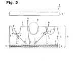
- Figs. 1(a) and 2 show a transmissive liquid crystal display unit 1 that includes a liquid crystal member and an area light emitting device.
- the liquid crystal member is a liquid crystal panel 2
- the area light emitting device is a backlight 3.
- the liquid crystal panel 2 has a conventional configuration, and, for example, includes pixels arranged in a matrix. Each pixel has color filters of red, blue and green.
- the liquid crystal panel 2 creates an image using the pixels.
- the backlight 3 is formed of a transparent substrate 5, and an organic electroluminescent element 4, which is an area light emitting element provided on the transparent substrate 5.
- the transparent substrate 5 is made of glass and has a thickness of 500 ⁇ m.
- the transparent substrate 5 permits part of or all visible light to pass through.
- the transparent substrate 5 has an incidence surface 6 and a light exit surface 7, which are located at opposite sides of the transparent substrate 5 with respect to each other.
- the incidence surface 6 is contained in the interface between the organic electroluminescent element 4 and the transparent substrate 5.
- the light exit surface 7 is contained in the interface between the transparent substrate 5 and the air.
- the incidence surface 6 is flat and faces the organic electroluminescent element 4.
- the light exit surface 7 faces away from the organic electroluminescent element 4, and is uneven with regularly arranged recesses 8. A part of the light exit surface 7 where no recesses 8 are formed is perpendicular to the thickness direction of the transparent substrate 5 and parallel to the incidence surface 6.
- the recesses 8 have the same semi-spheroidal shape in the same size. As shown in Fig. 1(b), each recess 8 has a circular opening. The diameter of the opening and the depth of the recess 8 are both 250 ⁇ m. Except for the recesses 8 located at the periphery of the light exit surface 7, each recess 8 is surrounded by other six recesses 8. Each adjacent pair of the recesses 8 is spaced by 50 ⁇ m.
- the recesses 8 are formed in the following manner. First, the transparent substrate 5, on which the organic electroluminescent element 4 is formed, is prepared. Before the recesses 8 are formed, the light exit surface 7 is perpendicular to the thickness direction of the transparent substrate 5 and parallel to the incidence surface 6. To prevent the organic electroluminescent element 4 from being scratched, the organic electroluminescent element 4 is sealed with a sealing member (not shown). Then, a part of the light exit surface 7 other than sections corresponding to the recesses 8 is protected with a mask. In this state, the light exit surface 7 is sandblasted. Accordingly, the portions of the light exit surface 7 that are not protected with the mask are ground so that the recesses 8 are formed. The mask is removed after the sandblasting.
- each section of the light exit surface 7 between an adjacent pair of the recesses 8 is not ground with sandblasting media, and stays perpendicular to the thickness direction of the transparent substrate 5 and parallel to the incidence surface 6.
- the organic electroluminescent element 4 includes a flat transparent electrode made of indium tin oxide (ITO), an organic layer including a flat light emitting layer 9, and a flat metal electrode, which are subsequently formed on the transparent substrate 5.
- ITO indium tin oxide
- the entire light emitting layer 9 of the organic electroluminescent element 4 simultaneously emit light of the same color.
- the light emitting layer 9 emits white light.
- Light emitted from the light emitting layer 9 advances to the transparent substrate 5 through the incidence surface 6 and then advances to the outside of the transparent substrate 5 through the light exit surface 7.
- the backlight 3 emits light emitted from the organic electroluminescent element 4 through the light exit surface 7.
- emission points on the organic electroluminescent element 4 are assumed to continuously exist on a plane parallel to the incidence surface 6 of the transparent substrate 5. Each emission point emits light evenly in all directions. Therefore, light emitted from the light emitting layer 9 enters the incidence surface 6 at every angle.
- An arrow A in Fig. 2 represents a ray of a portion of light from the back of the incidence surface 6.
- the emission angle of the ray of the arrow A is less than the critical angle at the interface between the transparent substrate 5 and air. If the ray of the arrow A reaches the back of the light exit surface 7 where no recesses 8 are formed, the ray is not totally reflected on the interface between the transparent substrate 5 and air and exits the substrate 5 through the light exit surface 7.
- Arrows B in Fig. 2 represent rays of portions of light from the back of the incidence surface 6.
- the emission angles of the rays of the arrows B are equal to or greater than the critical angle at the interface between the transparent substrate 5 and air. If the rays of the arrows B reach the back of the light exit surface 7 where no recesses 8 are formed, the rays are totally reflected on the interface between the transparent substrate 5 and air and does not exit the substrate 5 through the light exit surface 7. However, depending on the conditions, the rays represented by the arrows B, which reach the back of the light exit surface 7 where the recesses 8 are formed, are not totally reflected on the interface between the transparent substrate 5 and air but exit the substrate 5 through the light exit surface 7.
- This embodiment provides the following advantages.
- the area light emitting device forming the backlight 3, or the organic electroluminescent element 4, may be replaced by an inorganic electroluminescent element. This modification also has the advantages of the illustrated embodiment.
- the recesses 8 are formed in the transparent substrate 5, which has been formed as a flat plate.
- the recesses 8 may be formed at the same time when the transparent substrate 5 is molded using a mold. This modification also has the advantages of the illustrated embodiment.
- the recesses 8 are formed through sandblasting.
- the recesses 8 may be formed through etching. This modification also has the advantages of the illustrated embodiment.
- photolithography is typically employed.
- the formation of the recesses 8 through photolithography is more complicated than a method using sandblasting.
- the area light emitting device is used as the backlight 3 of the liquid crystal display unit 1.
- the area light emitting device may be applied to other purposes such as lighting devices. This modification also has the advantages of the illustrated embodiment.
- the color of light emitted by the organic electroluminescent element 4 need not be white, but may be any color. This modification also has the advantages of the illustrated embodiment.
- the transparent substrate 5 need not be made of glass, but may be made of a resin. This modification also has the advantages of the illustrated embodiment.
- a backlight in a liquid crystal display unit has a transparent substrate and an organic electroluminescent element provided on the transparent substrate.
- the backlight emits light emitted from the organic electroluminescent element from a light exit surface of the transparent substrate.
- a plurality of recesses are formed in the light exit surface. A part of the light exit surface between each adjacent pair of the recesses includes a plane that is perpendicular to the thickness direction of the transparent substrate. The backlight permits light emitted from the organic electroluminescent element to be efficiently emitted.
Abstract
A backlight in a liquid crystal display unit according
to the present invention has a transparent substrate and an
organic electroluminescent element provided on the transparent
substrate. The backlight emits light emitted from the organic
electroluminescent element from a light exit surface of the
transparent substrate. A plurality of recesses are formed in
the light exit surface. A part of the light exit surface
between each adjacent pair of the recesses includes a plane
that is perpendicular to the thickness direction of the
transparent substrate. The backlight permits light emitted
from the organic electroluminescent element to be efficiently
emitted.
Description
- The present invention relates to an area light emitting device emitting light through an area, a method for manufacturing such a light emitting device, and a liquid crystal display unit having such a light emitting device.
- A typical area light emitting device has an area light emitting element emitting light through an area. Light from such an area light emitting element is emitted through a flat substrate. In this case, only 20 to 25% of light from the light emitting element exits the light emitting device. That is, the light emitting device is unable to efficiently emit light emitted from the light emitting element. This is because a great proportion of light from the light emitting element is reflected on an interface between the flat substrate and air.
- In an organic EL device disclosed in Fig. 11 of Japanese Laid-Open Patent Publication No. 2001-135477, a plano-convex lens is formed in each section of a substrate that corresponds to a pixel, thereby increasing the proportion of light that exits the organic EL device. In the light emitting device disclosed in Japanese Laid-Open Patent Publication No. 2002-8850, light scatterers, which are asperities formed by etching a transparent film, are provided on a substrate to increase the proportion of light that exits the light emitting device.
- Accordingly, it is an objective of the present invention to provide a novel area light emitting device that is capable of efficiently emitting light emitted from a light emitting element, and a method for manufacturing such an area light emitting device. Another objective of the present invention is to provide a liquid crystal display unit provided with such an area light emitting device.
- To achieve the foregoing and other objectives and in accordance with the purpose of the present invention, an area light emitting device is provided. The device includes a transparent substrate having a predetermined thickness and an area light emitting element provided on the transparent substrate. The transparent substrate includes a light exit surface. Light emitted from the element advances through the transparent substrate and exits the device through the light exit surface. A plurality of recesses are located on the light exit surface. A part of the light exit surface between each adjacent pair of the recesses includes a plane that is perpendicular to the thickness direction of the transparent substrate.
- The present invention also provides another area light emitting device. The device includes a transparent substrate and an area light emitting element provided on the transparent substrate. The transparent substrate includes a light exit surface. Light emitted from the element advances through the transparent substrate and exits the device through the light exit surface. A plurality of recesses are located on the light exit surface. The recesses are formed by processing the light exit surface. A part of the light exit surface between each adjacent pair of the recesses includes a portion that is not subjected to the process for forming the recesses.
- In another aspect of the present invention, a method for manufacturing an area light emitting device is provided. The device includes a transparent substrate and an area light emitting element provided on the transparent substrate. The transparent substrate includes a light exit surface. Light emitted from the element advances through the transparent substrate and exits the device through the light exit surface. The method includes: masking a part of the light exit surface with a mask; sandblasting the light exit surface, which is masked, thereby forming a plurality of recesses in the light exit surface; and removing the mask after the sandblasting.
- The present invention provides another method for manufacturing an area light emitting device. The device includes a transparent substrate and an organic electroluminescent element. The transparent substrate includes a light exit surface. Light emitted from the element advances through the transparent substrate and exits the device through the light exit surface. The method includes: forming the organic electroluminescent element on the transparent substrate; sealing the organic electroluminescent element on the transparent substrate; masking a part of the light exit surface of the transparent substrate, on which the organic electroluminescent element is formed, with a mask; sandblasting the light exit surface, which is masked, thereby forming a plurality of recesses in the light exit surface; and removing the mask after the sandblasting.
- Other aspects and advantages of the invention will become apparent from the following description, taken in conjunction with the accompanying drawings, illustrating by way of example the principles of the invention.
- The invention, together with objects and advantages thereof, may best be understood by reference to the following description of the presently preferred embodiments together with the accompanying drawings in which:
- Fig. 1(a) is a diagrammatic cross-sectional view showing a liquid crystal display unit according to one embodiment of the present invention;
- Fig. 1(b) is a plan view showing a portion of a transparent substrate of the liquid crystal display unit shown in Fig. 1(a);
- Fig. 1(c) is a cross-sectional view showing recesses in the liquid crystal display unit shown in Fig. 1(a); and
- Fig. 2 is a schematic cross-sectional view for explaining paths of light in the liquid crystal display unit shown in Fig. 1(a).
-
- One embodiment of the present invention will now be described with reference to Figs. 1(a) to 2.
- Figs. 1(a) and 2 show a transmissive liquid
crystal display unit 1 that includes a liquid crystal member and an area light emitting device. In this embodiment, the liquid crystal member is aliquid crystal panel 2, and the area light emitting device is abacklight 3. Theliquid crystal panel 2 has a conventional configuration, and, for example, includes pixels arranged in a matrix. Each pixel has color filters of red, blue and green. Theliquid crystal panel 2 creates an image using the pixels. Thebacklight 3 is formed of atransparent substrate 5, and an organicelectroluminescent element 4, which is an area light emitting element provided on thetransparent substrate 5. - The
transparent substrate 5 is made of glass and has a thickness of 500 µm. Thetransparent substrate 5 permits part of or all visible light to pass through. Thetransparent substrate 5 has anincidence surface 6 and alight exit surface 7, which are located at opposite sides of thetransparent substrate 5 with respect to each other. Theincidence surface 6 is contained in the interface between the organicelectroluminescent element 4 and thetransparent substrate 5. Thelight exit surface 7 is contained in the interface between thetransparent substrate 5 and the air. - The
incidence surface 6 is flat and faces the organicelectroluminescent element 4. Thelight exit surface 7 faces away from the organicelectroluminescent element 4, and is uneven with regularly arrangedrecesses 8. A part of thelight exit surface 7 where norecesses 8 are formed is perpendicular to the thickness direction of thetransparent substrate 5 and parallel to theincidence surface 6. - The
recesses 8 have the same semi-spheroidal shape in the same size. As shown in Fig. 1(b), eachrecess 8 has a circular opening. The diameter of the opening and the depth of therecess 8 are both 250 µm. Except for therecesses 8 located at the periphery of thelight exit surface 7, eachrecess 8 is surrounded by other sixrecesses 8. Each adjacent pair of therecesses 8 is spaced by 50 µm. - The
recesses 8 are formed in the following manner. First, thetransparent substrate 5, on which the organicelectroluminescent element 4 is formed, is prepared. Before therecesses 8 are formed, thelight exit surface 7 is perpendicular to the thickness direction of thetransparent substrate 5 and parallel to theincidence surface 6. To prevent theorganic electroluminescent element 4 from being scratched, theorganic electroluminescent element 4 is sealed with a sealing member (not shown). Then, a part of thelight exit surface 7 other than sections corresponding to therecesses 8 is protected with a mask. In this state, thelight exit surface 7 is sandblasted. Accordingly, the portions of thelight exit surface 7 that are not protected with the mask are ground so that therecesses 8 are formed. The mask is removed after the sandblasting. - Since the
recesses 8 are formed in the above described manner, each section of thelight exit surface 7 between an adjacent pair of therecesses 8 is not ground with sandblasting media, and stays perpendicular to the thickness direction of thetransparent substrate 5 and parallel to theincidence surface 6. - The
organic electroluminescent element 4 includes a flat transparent electrode made of indium tin oxide (ITO), an organic layer including a flat light emitting layer 9, and a flat metal electrode, which are subsequently formed on thetransparent substrate 5. When voltage applied to the transparent electrode and the metal electrode, the entire light emitting layer 9 of theorganic electroluminescent element 4 simultaneously emit light of the same color. In this embodiment, the light emitting layer 9 emits white light. Light emitted from the light emitting layer 9 advances to thetransparent substrate 5 through theincidence surface 6 and then advances to the outside of thetransparent substrate 5 through thelight exit surface 7. In other words, thebacklight 3 emits light emitted from theorganic electroluminescent element 4 through thelight exit surface 7. - The operation of the liquid
crystal display unit 1 will now be described with reference to Fig. 2. - Since the light emitting layer 9 is flat, emission points on the
organic electroluminescent element 4 are assumed to continuously exist on a plane parallel to theincidence surface 6 of thetransparent substrate 5. Each emission point emits light evenly in all directions. Therefore, light emitted from the light emitting layer 9 enters theincidence surface 6 at every angle. - An arrow A in Fig. 2 represents a ray of a portion of light from the back of the
incidence surface 6. The emission angle of the ray of the arrow A is less than the critical angle at the interface between thetransparent substrate 5 and air. If the ray of the arrow A reaches the back of thelight exit surface 7 where norecesses 8 are formed, the ray is not totally reflected on the interface between thetransparent substrate 5 and air and exits thesubstrate 5 through thelight exit surface 7. - Arrows B in Fig. 2 represent rays of portions of light from the back of the
incidence surface 6. The emission angles of the rays of the arrows B are equal to or greater than the critical angle at the interface between thetransparent substrate 5 and air. If the rays of the arrows B reach the back of thelight exit surface 7 where norecesses 8 are formed, the rays are totally reflected on the interface between thetransparent substrate 5 and air and does not exit thesubstrate 5 through thelight exit surface 7. However, depending on the conditions, the rays represented by the arrows B, which reach the back of thelight exit surface 7 where therecesses 8 are formed, are not totally reflected on the interface between thetransparent substrate 5 and air but exit thesubstrate 5 through thelight exit surface 7. This is because whether light that reaches the back of thelight exit surface 7 where therecess 8 is formed is totally reflected is determined by an incident angle (for example, an angle y and an angle p in Fig. 2) relative to a tangent plane (for example, planes containing lines b in Fig. 2) at the point of incidence (for example, points a in Fig. 2). That is, as long as the incidence angle is less than the critical angle, even if the emission angle is equal to or greater than the critical angle, light is not totally reflected on the interface between thetransparent substrate 5 and air but exits thesubstrate 5 through thelight exit surface 7. In this manner, light that would not be emitted from thelight exit surface 7 if norecesses 8 were formed is permitted to exit thesubstrate 5 through thelight exit surface 7. Accordingly, light emitted from theorganic electroluminescent element 4 is efficiently emitted. - This embodiment provides the following advantages.
- (1) According to the illustrated embodiment, even if the
emission angle at the back of the
incidence surface 6 is greater than the critical angle of the interface between thetransparent substrate 5 and air, a part of such light is not totally reflected on the interface but exits thesubstrate 5 through thelight exit surface 7. Therefore, light emitted from theorganic electroluminescent element 4 is efficiently emitted. - (2) Each
recess 8 formed in thelight exit surface 7 is semi-spheroidal shape and has rotation symmetry. Therefore, any light that reaches the back of thelight exit surface 7 where therecess 8 is formed behaves in the same manner regardless of the direction of incidence. - (3) The
recesses 8 are regularly formed so that eachrecess 8 is surrounded by other six of therecesses 8. That is, therecesses 8 are arranged in the densest manner. The illustrated embodiment therefore maximizes the advantages of therecesses 8. - (4) Instead of sandblasting, the
recesses 8 may be etched through photolithography. However, photolithography requires a relatively great number of processes compared to sandblasting, which only has the masking process and the blasting process. That is, the formation of therecesses 8 using sandblasting is simpler than a method using photolithography. If photolithography is used, a pattern made of a photosensitive material needs to be formed on thetransparent substrate 5 through a number of processes: a process for forming a layer of the photosensitive material on thetransparent substrate 5; a process of pre-baking; a process for forming a latent image in the photosensitive layer through irradiation of light; a developing process; and a post-baking process. In addition, if photolithography is used, the number of types of materials that can be used for the sealing material is significantly limited. Also, means for preventing chemical agents used in photolithography from entering theorganic electroluminescent element 4 is required. - (5) A part of the
light exit surface 7 where norecesses 8 are formed is perpendicular to the thickness direction of thetransparent substrate 5 and parallel to theincidence surface 6. Therefore, when light the emission angle of which at the back of theincidence surface 6 is less than the critical angle at the interface between theexit substrate 5 and air reaches such part, the light is not totally reflected but exits thesubstrate 5 through thelight exit surface 7. - (6) A part of the
light exit surface 7 where norecesses 8 are formed is not divided but formed continuously. Therefore, stress applied on thetransparent substrate 5 during installment or use is spread out over the entire part of thelight exit surface 7 where norecesses 8 are formed. Therefore, the mechanical strength of thetransparent substrate 5 is not significantly reduced by forming therecesses 8 in thetransparent substrate 5. - (7) The
backlight 3 efficiently emits light emitted from theorganic electroluminescent element 4. Therefore, the liquidcrystal display unit 1 with thebacklight 3 is capable of improving the viewability of displayed images. - (8) The
recesses 8 are easily formed through sandblasting on thetransparent substrate 5, on which theorganic electroluminescent element 4 is formed in advance. - (9) A case where a film having recesses is provided on
the
transparent substrate 5 instead of forming therecesses 8 in thelight exit surface 7 of thetransparent substrate 5 will now be discussed. This configuration seemingly permits light emitted from theorganic electroluminescent element 4 to be efficiently emitted by the backlight. However, in reality, since a part of light is reflected on the interface between thetransparent substrate 5 and the film, light emitted from theorganic electroluminescent element 4 is not as efficiently emitted by the backlight as the illustrated embodiment. That is, the number of interfaces between substances of different refractive indexes is preferably minimized in the path of light that is emitted from theorganic electroluminescent element 4 and emitted from the backlight. -
- It should be apparent to those skilled in the art that the present invention may be embodied in many other specific forms without departing from the spirit of scope of the invention. Particularly, it should be understood that the invention may be embodied in the following forms.
- The area light emitting device forming the
backlight 3, or theorganic electroluminescent element 4, may be replaced by an inorganic electroluminescent element. This modification also has the advantages of the illustrated embodiment. - In the illustrated embodiment, the
recesses 8 are formed in thetransparent substrate 5, which has been formed as a flat plate. However, therecesses 8 may be formed at the same time when thetransparent substrate 5 is molded using a mold. This modification also has the advantages of the illustrated embodiment. - In the illustrated embodiment, the
recesses 8 are formed through sandblasting. However, therecesses 8 may be formed through etching. This modification also has the advantages of the illustrated embodiment. When therecesses 8 are formed through etching, photolithography is typically employed. However, the formation of therecesses 8 through photolithography is more complicated than a method using sandblasting. - In the illustrated embodiment, the area light emitting device is used as the
backlight 3 of the liquidcrystal display unit 1. The area light emitting device may be applied to other purposes such as lighting devices. This modification also has the advantages of the illustrated embodiment. - The color of light emitted by the
organic electroluminescent element 4 need not be white, but may be any color. This modification also has the advantages of the illustrated embodiment. - The
transparent substrate 5 need not be made of glass, but may be made of a resin. This modification also has the advantages of the illustrated embodiment. - The present examples and embodiments are to be considered as illustrative and not restrictive and the invention is not to be limited to the details given herein, but may be modified within the scope and equivalence of the appended claims.
- A backlight in a liquid crystal display unit according to the present invention has a transparent substrate and an organic electroluminescent element provided on the transparent substrate. The backlight emits light emitted from the organic electroluminescent element from a light exit surface of the transparent substrate. A plurality of recesses are formed in the light exit surface. A part of the light exit surface between each adjacent pair of the recesses includes a plane that is perpendicular to the thickness direction of the transparent substrate. The backlight permits light emitted from the organic electroluminescent element to be efficiently emitted.
Claims (17)
- An area light emitting device, characterized by a transparent substrate having a predetermined thickness and an area light emitting element provided on the transparent substrate, wherein the transparent substrate includes a light exit surface, wherein light emitted from the element advances through the transparent substrate and exits the device through the light exit surface, wherein a plurality of recesses are located on the light exit surface, and wherein a part of the light exit surface between each adjacent pair of the recesses includes a plane that is perpendicular to the thickness direction of the transparent substrate.
- The area light emitting device according to claim 1, characterized in that, except for the recesses located at the periphery of the light exit surface, each recess is surrounded by other six recesses.
- The area light emitting device according to claim 1 or 2, characterized in that the element is an organic electroluminescent element.
- The area light emitting device according to any one of claims 1 to 3, characterized in that a cross-section of each recess along a plane that is perpendicular to the thickness direction of the transparent substrate is circular.
- The area light emitting device according to claim 4, characterized in that each recess has a circular opening, and wherein the diameter of the opening is approximately half the thickness of the transparent substrate.
- The area light emitting device according to any one of claims 1 to 5, characterized in that the depth of each recess is approximately half the thickness of the transparent substrate.
- The area light emitting device according to any one of claims 1 to 6, characterized in that the cross-sectional area of each recess decreases toward the element.
- The area light emitting device according to any one of claims 1 to 7, characterized in that the bottom of each recess is shaped as a curved surface.
- A liquid crystal display unit, characterized by a liquid crystal member and the area light emitting device according to any one of claims 1 to 8, wherein the liquid crystal member creates images by using light emitted by the area light emitting device.
- An area light emitting device, characterized by a transparent substrate and an area light emitting element provided on the transparent substrate, wherein the transparent substrate includes a light exit surface, wherein light emitted from the element advances through the transparent substrate and exits the device through the light exit surface, wherein a plurality of recesses are located on the light exit surface, the recesses being formed by processing the light exit surface , and wherein a part of the light exit surface between each adjacent pair of the recesses includes a portion that is not subjected to the process for forming the recesses.
- The area light emitting device according to claim 10, characterized in that the process for forming the recesses is sandblasting.
- The area light emitting device according to claim 11, characterized in that the sandblasting is performed on the light exit surface of the transparent substrate, on which the element has been formed in advance.
- The area light emitting device according to any one of claims 10 to 12, characterized in that, except for the recesses located at the periphery of the light exit surface, each recess is surrounded by other six recesses.
- The area light emitting device according to any one of claims 10 to 13, characterized in that the element is an organic electroluminescent element.
- A liquid crystal display unit, characterized by a liquid crystal member and the area light emitting device according to any one of claims 10 to 14, wherein the liquid crystal member creates images by using light emitted by the area light emitting device.
- A method for manufacturing an area light emitting device, wherein the device includes a transparent substrate and an area light emitting element provided on the transparent substrate, wherein the transparent substrate includes a light exit surface, and wherein light emitted from the element advances through the transparent substrate and exits the device through the light exit surface, the method characterized by:masking a part of the light exit surface with a mask;sandblasting the light exit surface, which is masked, thereby forming a plurality of recesses in the light exit surface; andremoving the mask after the sandblasting.
- A method for manufacturing an area light emitting device, wherein the device includes a transparent substrate and an organic electroluminescent element, wherein the transparent substrate includes a light exit surface, and wherein light emitted from the element advances through the transparent substrate and exits the device through the light exit surface, the method characterized by:forming the organic electroluminescent element on the transparent substrate;sealing the organic electroluminescent element on the transparent substrate;masking a part of the light exit surface of the transparent substrate, on which the organic electroluminescent element is formed , with a mask;sandblasting the light exit surface, which is masked, thereby forming a plurality of recesses in the light exit surface; andremoving the mask after the sandblasting.
Applications Claiming Priority (2)
| Application Number | Priority Date | Filing Date | Title |
|---|---|---|---|
| JP2003040632 | 2003-02-19 | ||
| JP2003040632A JP2004253199A (en) | 2003-02-19 | 2003-02-19 | Planar luminescent device, its manufacturing method, and liquid crystal display device |
Publications (1)
| Publication Number | Publication Date |
|---|---|
| EP1450418A2 true EP1450418A2 (en) | 2004-08-25 |
Family
ID=32732933
Family Applications (1)
| Application Number | Title | Priority Date | Filing Date |
|---|---|---|---|
| EP04003656A Withdrawn EP1450418A2 (en) | 2003-02-19 | 2004-02-18 | Area light emitting device, method for manufacturing the same, and liquid crystal display unit |
Country Status (6)
| Country | Link |
|---|---|
| US (1) | US20040160787A1 (en) |
| EP (1) | EP1450418A2 (en) |
| JP (1) | JP2004253199A (en) |
| KR (1) | KR100587746B1 (en) |
| CN (1) | CN1525798A (en) |
| TW (1) | TWI245584B (en) |
Cited By (20)
| Publication number | Priority date | Publication date | Assignee | Title |
|---|---|---|---|---|
| WO2006036496A1 (en) * | 2004-09-27 | 2006-04-06 | Idc, Llc | Optical films for directing light towards active areas of displays |
| US7349141B2 (en) | 2004-09-27 | 2008-03-25 | Idc, Llc | Method and post structures for interferometric modulation |
| US7706050B2 (en) | 2004-03-05 | 2010-04-27 | Qualcomm Mems Technologies, Inc. | Integrated modulator illumination |
| US7710632B2 (en) | 2004-09-27 | 2010-05-04 | Qualcomm Mems Technologies, Inc. | Display device having an array of spatial light modulators with integrated color filters |
| US7750886B2 (en) | 2004-09-27 | 2010-07-06 | Qualcomm Mems Technologies, Inc. | Methods and devices for lighting displays |
| US7766498B2 (en) | 2006-06-21 | 2010-08-03 | Qualcomm Mems Technologies, Inc. | Linear solid state illuminator |
| US7807488B2 (en) | 2004-09-27 | 2010-10-05 | Qualcomm Mems Technologies, Inc. | Display element having filter material diffused in a substrate of the display element |
| US7813026B2 (en) | 2004-09-27 | 2010-10-12 | Qualcomm Mems Technologies, Inc. | System and method of reducing color shift in a display |
| US7949213B2 (en) | 2007-12-07 | 2011-05-24 | Qualcomm Mems Technologies, Inc. | Light illumination of displays with front light guide and coupling elements |
| US8040588B2 (en) | 2004-09-27 | 2011-10-18 | Qualcomm Mems Technologies, Inc. | System and method of illuminating interferometric modulators using backlighting |
| US8045252B2 (en) | 2004-02-03 | 2011-10-25 | Qualcomm Mems Technologies, Inc. | Spatial light modulator with integrated optical compensation structure |
| US8049951B2 (en) | 2008-04-15 | 2011-11-01 | Qualcomm Mems Technologies, Inc. | Light with bi-directional propagation |
| US8172417B2 (en) | 2009-03-06 | 2012-05-08 | Qualcomm Mems Technologies, Inc. | Shaped frontlight reflector for use with display |
| US8538665B2 (en) | 2008-04-24 | 2013-09-17 | Continental Automotive Gmbh | Control circuit for an electrochemical gas sensor and method for adjusting an electrochemical gas sensor |
| US8798425B2 (en) | 2007-12-07 | 2014-08-05 | Qualcomm Mems Technologies, Inc. | Decoupled holographic film and diffuser |
| US8848294B2 (en) | 2010-05-20 | 2014-09-30 | Qualcomm Mems Technologies, Inc. | Method and structure capable of changing color saturation |
| US8872085B2 (en) | 2006-10-06 | 2014-10-28 | Qualcomm Mems Technologies, Inc. | Display device having front illuminator with turning features |
| US8979349B2 (en) | 2009-05-29 | 2015-03-17 | Qualcomm Mems Technologies, Inc. | Illumination devices and methods of fabrication thereof |
| US9019183B2 (en) | 2006-10-06 | 2015-04-28 | Qualcomm Mems Technologies, Inc. | Optical loss structure integrated in an illumination apparatus |
| US9025235B2 (en) | 2002-12-25 | 2015-05-05 | Qualcomm Mems Technologies, Inc. | Optical interference type of color display having optical diffusion layer between substrate and electrode |
Families Citing this family (6)
| Publication number | Priority date | Publication date | Assignee | Title |
|---|---|---|---|---|
| KR100781616B1 (en) * | 2006-04-07 | 2007-12-05 | 네오뷰코오롱 주식회사 | display equipment including glass insulator and glass insulator manufacture and Organic Light Emitting Diodes manufacture using glass insulator |
| CN100437154C (en) * | 2007-03-13 | 2008-11-26 | 友达光电股份有限公司 | Light source diffusion plate and backlight module |
| JP2010040211A (en) * | 2008-07-31 | 2010-02-18 | Sumitomo Chemical Co Ltd | Organic electroluminescent element, method of manufacturing the same, lighting system, planar light source, and display device |
| JP2010219006A (en) * | 2009-03-19 | 2010-09-30 | Toppan Printing Co Ltd | El element, backlight device, lighting system, electronic signboard device, and display device |
| US8687145B2 (en) | 2010-08-13 | 2014-04-01 | Lg Chem, Ltd. | Organic electroluminescent device and method for fabricating the same |
| KR102516687B1 (en) * | 2015-09-30 | 2023-03-30 | 엘지디스플레이 주식회사 | Reflective control film and display apparatus comprising the same |
Family Cites Families (1)
| Publication number | Priority date | Publication date | Assignee | Title |
|---|---|---|---|---|
| JP2001004998A (en) * | 1999-06-24 | 2001-01-12 | Nec Corp | Liquid crystal display device |
-
2003
- 2003-02-19 JP JP2003040632A patent/JP2004253199A/en active Pending
-
2004
- 2004-02-12 KR KR1020040009347A patent/KR100587746B1/en not_active IP Right Cessation
- 2004-02-13 US US10/778,962 patent/US20040160787A1/en not_active Abandoned
- 2004-02-16 TW TW093103584A patent/TWI245584B/en not_active IP Right Cessation
- 2004-02-18 EP EP04003656A patent/EP1450418A2/en not_active Withdrawn
- 2004-02-18 CN CNA2004100283168A patent/CN1525798A/en active Pending
Cited By (25)
| Publication number | Priority date | Publication date | Assignee | Title |
|---|---|---|---|---|
| US9025235B2 (en) | 2002-12-25 | 2015-05-05 | Qualcomm Mems Technologies, Inc. | Optical interference type of color display having optical diffusion layer between substrate and electrode |
| US9019590B2 (en) | 2004-02-03 | 2015-04-28 | Qualcomm Mems Technologies, Inc. | Spatial light modulator with integrated optical compensation structure |
| US8111445B2 (en) | 2004-02-03 | 2012-02-07 | Qualcomm Mems Technologies, Inc. | Spatial light modulator with integrated optical compensation structure |
| US8045252B2 (en) | 2004-02-03 | 2011-10-25 | Qualcomm Mems Technologies, Inc. | Spatial light modulator with integrated optical compensation structure |
| US7880954B2 (en) | 2004-03-05 | 2011-02-01 | Qualcomm Mems Technologies, Inc. | Integrated modulator illumination |
| US7706050B2 (en) | 2004-03-05 | 2010-04-27 | Qualcomm Mems Technologies, Inc. | Integrated modulator illumination |
| US7710632B2 (en) | 2004-09-27 | 2010-05-04 | Qualcomm Mems Technologies, Inc. | Display device having an array of spatial light modulators with integrated color filters |
| US7807488B2 (en) | 2004-09-27 | 2010-10-05 | Qualcomm Mems Technologies, Inc. | Display element having filter material diffused in a substrate of the display element |
| US7813026B2 (en) | 2004-09-27 | 2010-10-12 | Qualcomm Mems Technologies, Inc. | System and method of reducing color shift in a display |
| WO2006036496A1 (en) * | 2004-09-27 | 2006-04-06 | Idc, Llc | Optical films for directing light towards active areas of displays |
| US7750886B2 (en) | 2004-09-27 | 2010-07-06 | Qualcomm Mems Technologies, Inc. | Methods and devices for lighting displays |
| US8040588B2 (en) | 2004-09-27 | 2011-10-18 | Qualcomm Mems Technologies, Inc. | System and method of illuminating interferometric modulators using backlighting |
| US7719747B2 (en) | 2004-09-27 | 2010-05-18 | Qualcomm Mems Technologies, Inc. | Method and post structures for interferometric modulation |
| US7349141B2 (en) | 2004-09-27 | 2008-03-25 | Idc, Llc | Method and post structures for interferometric modulation |
| US7766498B2 (en) | 2006-06-21 | 2010-08-03 | Qualcomm Mems Technologies, Inc. | Linear solid state illuminator |
| US8872085B2 (en) | 2006-10-06 | 2014-10-28 | Qualcomm Mems Technologies, Inc. | Display device having front illuminator with turning features |
| US9019183B2 (en) | 2006-10-06 | 2015-04-28 | Qualcomm Mems Technologies, Inc. | Optical loss structure integrated in an illumination apparatus |
| US8798425B2 (en) | 2007-12-07 | 2014-08-05 | Qualcomm Mems Technologies, Inc. | Decoupled holographic film and diffuser |
| US7949213B2 (en) | 2007-12-07 | 2011-05-24 | Qualcomm Mems Technologies, Inc. | Light illumination of displays with front light guide and coupling elements |
| US8049951B2 (en) | 2008-04-15 | 2011-11-01 | Qualcomm Mems Technologies, Inc. | Light with bi-directional propagation |
| US8538665B2 (en) | 2008-04-24 | 2013-09-17 | Continental Automotive Gmbh | Control circuit for an electrochemical gas sensor and method for adjusting an electrochemical gas sensor |
| US8172417B2 (en) | 2009-03-06 | 2012-05-08 | Qualcomm Mems Technologies, Inc. | Shaped frontlight reflector for use with display |
| US8979349B2 (en) | 2009-05-29 | 2015-03-17 | Qualcomm Mems Technologies, Inc. | Illumination devices and methods of fabrication thereof |
| US9121979B2 (en) | 2009-05-29 | 2015-09-01 | Qualcomm Mems Technologies, Inc. | Illumination devices and methods of fabrication thereof |
| US8848294B2 (en) | 2010-05-20 | 2014-09-30 | Qualcomm Mems Technologies, Inc. | Method and structure capable of changing color saturation |
Also Published As
| Publication number | Publication date |
|---|---|
| TWI245584B (en) | 2005-12-11 |
| JP2004253199A (en) | 2004-09-09 |
| US20040160787A1 (en) | 2004-08-19 |
| KR20040074606A (en) | 2004-08-25 |
| CN1525798A (en) | 2004-09-01 |
| TW200421930A (en) | 2004-10-16 |
| KR100587746B1 (en) | 2006-06-09 |
Similar Documents
| Publication | Publication Date | Title |
|---|---|---|
| EP1450418A2 (en) | Area light emitting device, method for manufacturing the same, and liquid crystal display unit | |
| US10141382B2 (en) | Method of manufacturing organic light emitting diode display panel having polymer network liquid crystal | |
| KR102113622B1 (en) | Display device and method for fabricating the same | |
| US9285629B2 (en) | Color-converting substrate and liquid crystal display device | |
| TWI395073B (en) | Exposure method and exposure apparatus for photosensitive film | |
| TWI502231B (en) | Display apparatus | |
| US10347698B2 (en) | Electrooptical device, manufacturing method of electrooptical device, and electronic equipment | |
| JP6686497B2 (en) | Electro-optical device and electronic equipment | |
| CN1746735A (en) | Display device and manufacture method thereof | |
| US20140321101A1 (en) | Color conversion substrate, display device, and color conversion substrate fabricating method | |
| US10670895B2 (en) | Cover glass, manufacturing method thereof, and display apparatus including the cover glass | |
| US6873380B2 (en) | Providing optical elements over emissive displays | |
| CN108628035B (en) | Photoluminescent device | |
| US20050151226A1 (en) | Transparent substrate for area light emitting device, a method for producing transparent substrate, and area light emitting device and liquid crystal display device | |
| US7433000B2 (en) | Lighting system and display | |
| US20120256562A1 (en) | Display apparatus | |
| US20140333988A1 (en) | Color filter structure and manufacturing method thereof | |
| KR20190143243A (en) | LED Module and backlight Module having the same and Display Device having the same | |
| JP2006171228A (en) | Color filter for self-luminous display device | |
| JPH09197106A (en) | Microarray lens array sheet and liquid crystal display device using that | |
| KR101660914B1 (en) | Flexible Display Device | |
| CN110816075B (en) | Printing head | |
| US20230157121A1 (en) | Display device and electronic device including the same | |
| CN113690281B (en) | Display panel | |
| CN114690470A (en) | Color filter substrate, manufacturing method thereof and liquid crystal display device |
Legal Events
| Date | Code | Title | Description |
|---|---|---|---|
| PUAI | Public reference made under article 153(3) epc to a published international application that has entered the european phase |
Free format text: ORIGINAL CODE: 0009012 |
|
| 17P | Request for examination filed |
Effective date: 20040218 |
|
| AK | Designated contracting states |
Kind code of ref document: A2 Designated state(s): AT BE BG CH CY CZ DE DK EE ES FI FR GB GR HU IE IT LI LU MC NL PT RO SE SI SK TR |
|
| AX | Request for extension of the european patent |
Extension state: AL LT LV MK |
|
| STAA | Information on the status of an ep patent application or granted ep patent |
Free format text: STATUS: THE APPLICATION HAS BEEN WITHDRAWN |
|
| 18W | Application withdrawn |
Effective date: 20070621 |