EP1413892A2 - Method and apparatus for measuringcharge carrier lifetime of a semiconductor wafer - Google Patents
Method and apparatus for measuringcharge carrier lifetime of a semiconductor wafer Download PDFInfo
- Publication number
- EP1413892A2 EP1413892A2 EP03078341A EP03078341A EP1413892A2 EP 1413892 A2 EP1413892 A2 EP 1413892A2 EP 03078341 A EP03078341 A EP 03078341A EP 03078341 A EP03078341 A EP 03078341A EP 1413892 A2 EP1413892 A2 EP 1413892A2
- Authority
- EP
- European Patent Office
- Prior art keywords
- semiconductor wafer
- capacitor
- voltage
- capacitance
- change
- Prior art date
- Legal status (The legal status is an assumption and is not a legal conclusion. Google has not performed a legal analysis and makes no representation as to the accuracy of the status listed.)
- Granted
Links
Images


Classifications
-
- G—PHYSICS
- G01—MEASURING; TESTING
- G01R—MEASURING ELECTRIC VARIABLES; MEASURING MAGNETIC VARIABLES
- G01R31/00—Arrangements for testing electric properties; Arrangements for locating electric faults; Arrangements for electrical testing characterised by what is being tested not provided for elsewhere
- G01R31/26—Testing of individual semiconductor devices
- G01R31/2648—Characterising semiconductor materials
-
- G—PHYSICS
- G01—MEASURING; TESTING
- G01N—INVESTIGATING OR ANALYSING MATERIALS BY DETERMINING THEIR CHEMICAL OR PHYSICAL PROPERTIES
- G01N27/00—Investigating or analysing materials by the use of electric, electrochemical, or magnetic means
- G01N27/02—Investigating or analysing materials by the use of electric, electrochemical, or magnetic means by investigating impedance
- G01N27/22—Investigating or analysing materials by the use of electric, electrochemical, or magnetic means by investigating impedance by investigating capacitance
Definitions
- the present invention relates to charge carrier lifetime measurement of product semiconductor wafers.
- the invention is a method of measuring a charge carrier lifetime of a semiconductor wafer that includes contacting an electrically conductive measurement probe to a surface of a semiconductor wafer to form a capacitor and applying a DC voltage having an AC voltage superimposed thereon between the measurement probe and the semiconductor wafer.
- the DC voltage is swept between a first voltage and a second voltage.
- the semiconductor wafer adjacent the contact between the measurement probe and surface of the semiconductor wafer is exposed to a light pulse. After the light pulse terminates, a change in capacitance of the capacitor over time is determined. From this thus determined change in capacitance, a charge carrier lifetime of the semiconductor wafer is determined.
- the semiconductor wafer can include a dielectric overlaying semiconductor material.
- the measurement probe contacts the dielectric to form the capacitor whereupon the measurement probe defines a first plate of the capacitor, the semiconductor material defines a second plate of the capacitor and the dielectric defines an electrical insulator therebetween.
- the measurement probe can include a dielectric that contacts a semiconductor wafer.
- the use of a measurement probe having dielectric enables formation of the capacitor when the probe is utilized to measure the charge carrier lifetime of a semiconductor wafer not having an overlaying dielectric.
- At least the part of the measurement probe that contacts the semiconductor wafer can be formed from an elastically deformable material.
- the capacitor has a minimum capacitance value.
- the capacitance value increases from the minimum capacitance value.
- the capacitance value decreases from the increased capacitance value to the minimum capacitance value.
- the step of determining a change in capacitance can include determining a time rate of change in the capacitance of the capacitor. This time rate of change in the capacitance of the capacitor can be utilized to determine the charge carrier lifetime of the semiconductor wafer.
- the time rate of change in the capacitance of the capacitor is preferably determined temporally adjacent the termination of the light pulse. However, this is not to be construed as limiting the invention.
- the exposure of the semiconductor wafer to the light pulse and the determination of the change in capacitance of the capacitor over time preferably occur in the presence of the second voltage.
- this is not to be construed as limiting the invention.
- the invention is also a semiconductor wafer charge carrier lifetime measuring apparatus.
- the apparatus includes an electrically conductive wafer chuck for supporting a backside of a semiconductor wafer and an electrically conductive measurement probe.
- a movement means is provided for moving the measurement probe and a topside of the semiconductor wafer into contact when the wafer chuck is supporting the semiconductor wafer.
- the contact between the semiconductor wafer and the measurement probe forms a capacitor.
- An electrical stimulus means is provided for applying a DC voltage having an AC voltage superimposed thereon to the capacitor and for sweeping the DC voltage from a first voltage to a second voltage.
- a light source supplies a light pulse to the semiconductor wafer adjacent the contact thereof with the measurement probe.
- a measurement means is provided for measuring a change in capacitance of the capacitor over time after the light pulse terminates and for determining from the change in capacitance over time a charge carrier lifetime of the semiconductor wafer.
- the measuring means determines a time rate of change in the capacitance of the capacitor and determines the charge carrier lifetime of the semiconductor wafer from the time rate of change in the capacitance of the capacitor.
- the invention is a method of measuring a charge carrier lifetime of a semiconductor wafer that includes forming a capacitor with a top surface of a semiconductor wafer and sweeping a test voltage applied to the capacitor from a first voltage to a second voltage. A light pulse is applied to the semiconductor wafer whereupon the capacitance of the capacitor increases. A time rate of change in a decay of the capacitance of the capacitor is determined and a charge carrier lifetime of the semiconductor wafer is determined from the thus determined time rate of change in the decay of the capacitance of the capacitor.
- Fig. 1(a) is a first embodiment of a semiconductor wafer charge carrier lifetime measuring apparatus
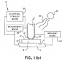
- Fig. 1(b) is a second embodiment of a semiconductor wafer charge carrier lifetime measuring apparatus
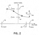
- Fig. 2 is a graph of capacitance versus voltage for the capacitor formed by the probe and semiconductor wafer in each of Figs. 1(a) and 1(b) in response to a voltage sweep and a light pulse;
- Fig. 3 is a graph of capacitance versus time for the capacitor formed by the probe and semiconductor wafer in each of Figs. 1(a) and 1(b) in response to the voltage sweep and the light pulse.
- a first embodiment apparatus 2 for measuring a semiconductor wafer charge carrier lifetime includes an electrically conductive chuck 4 and an elastically deformable, electrically conductive measurement probe 6.
- Chuck 4 is configured to support a backside 8 of a semiconductor wafer 10.
- a distal end 12 of probe 6 has a curved or arcuate surface for contacting a topside 14 of semiconductor wafer 10.
- a movement means 20 can be connected to chuck 4, probe 6 or both for moving distal end 12 of probe 6 and topside 14 of semiconductor wafer 10 into contact.
- An electrical stimulus means 22 is electrically connected between chuck 4 and probe 6 for applying a suitable test stimulus to semiconductor wafer 10 when it is received on chuck 4 and distal end 12 of probe 6 is in contact with topside 14 of semiconductor wafer 10.
- One suitable test stimulus is a CV-type electrical stimulus 24 of the type shown in Fig. 2 wherein a DC voltage 24 having an AC voltage (not shown) superimposed thereon is swept from a first voltage (V START ) 26, which is less than a threshold voltage (V T ) 28 of semiconductor wafer 10, to a second voltage (V MEAS ) 30 which is greater than threshold voltage 28.
- V START first voltage
- V T threshold voltage
- V MEAS second voltage
- the DC voltage is swept slowly enough to allow for minority carrier generation in the semiconductor material underlying the contact between probe 6 and semiconductor wafer 10.
- CV-type electrical stimulus 24 is for semiconductor wafer 10 formed from p-type silicon. A mirror-image of CV-type electrical stimulus 24 would be utilized for semiconductor wafer 10 formed from n-type silicon.
- Apparatus 2 includes a light source 34, such as a xenon lamp, which can be positioned to direct a light pulse 36 toward semiconductor wafer 10 adjacent the contact with probe 6.
- a measurement means 38 is connected between chuck 4 and probe 6 for measuring a response of semiconductor wafer 10 to light pulse 36 and for determining from this measurement a charge carrier lifetime of semiconductor wafer 10.
- semiconductor wafer 10 includes a dielectric 16 overlaying semiconductor material 18.
- topside 14 of semiconductor wafer 10 is the side of dielectric 16 opposite semiconductor material 18.
- a second embodiment apparatus 2' for measuring a charge carrier lifetime of a semiconductor wafer includes electrically deformable, electrically conductive probe 6' having a dielectric 16' covering at least its distal end 12'.
- the addition of dielectric 16' on electrically conductive probe 6' enables electrical measurements to be made directly on semiconductor material 18 of semiconductor wafer 10'. In other words, where semiconductor wafer 10' does not include dielectric overlaying semiconductor material 18, probe 6' having dielectric 16' over distal end 12' can contact top surface 14' of semiconductor material 18 directly.
- Probes 6 and 6' can be formed from any suitable material that is elastically deformable and electrically conductive.
- One suitable material is tantalum.
- at least distal end 12 of probe 6 is formed from tantalum and includes on its outer surface a native oxide layer that grows thereon in response to exposure to atmosphere.
- probe 6' is a tantalum probe and dielectric 16' is a thermally grown metallic oxide.
- dielectric 16' can be any suitable material having a high dielectric constant that can be grown or applied to the exterior surface .of probe 6' adjacent at least its distal end 12'. Suitable materials include those having dielectric constants greater than 3.9.
- One example of a grown dielectric is tantalum oxide.
- One example of an applied dielectric 16' is silicon rubber. However, these examples are not to be construed as limiting the invention since the use of any suitable grown or applied dielectric 16' is envisioned.
- contact between distal end 12 of probe 6 and top surface 14 of semiconductor wafer 10 forms a capacitor. More specifically, probe 6 defines a first plate of the capacitor, semiconductor material 18 defines a second plate of the capacitor and dielectric 16 defines an electrical insulator therebetween.
- contact between distal end 12' of probe 6' and topside 14' of semiconductor wafer 10' forms a capacitor.
- the electrically conductive portion of probe 6' defines a first plate of the capacitor, semiconductor material 18 defines a second plate of the capacitor and dielectric 16' defines the electrical insulator therebetween.
- the capacitance of the capacitor formed by probe 6 and semiconductor wafer 10 increases from minimum capacitance 42 to maximum capacitance 40 during a time interval 50 of light pulse 36.
- light pulse 36 terminates and electron-hole pairs generated in response to interaction between light pulse 36 and semiconductor material 18 of semiconductor wafer 10 commence recombination whereupon the capacitance of the capacitor formed by probe 6 and semiconductor wafer 10 commences decreasing from maximum capacitance 40 to minimum capacitance 42 over a time interval 52.
- the rate of this recombination and, hence, the decrease in capacitance depends highly on the defect and impurity concentration of semiconductor material 18.
- Measurement means 38 determines the change in capacitance of the capacitor over time and determines therefrom a charge carrier lifetime of semiconductor wafer 10. More specifically, measurement means 38 determines a time rate of change in the capacitance of the capacitor and determines from this time rate of change the charge carrier lifetime of semiconductor wafer 10.
- the time rate of change of the capacitance of the capacitor is determined temporally adjacent the termination of light pulse 36. To this end, the time rate of change in the capacitance of the capacitor is determined at the end of a time interval 54 after termination of light pulse 36.
- the time rate of change of the capacitance of the capacitor at the end of interval 54 can be correlated to the defect and impurity concentration of semiconductor material 18. It is preferable that measurement of the time rate of change in the capacitance of capacitors formed with different semiconductor wafers 10 occurs at approximately the same point in time after termination of light pulse 36 to enable correlation among the semiconductor wafers 10 with regard to defect and impurity concentration in the semiconductor materials thereof.
- this is not to be construed as limiting the invention.
- a solid line 60 shows a change in capacitance over time for a semiconductor material 18 having a high concentration of impurities and a dashed line 62 shows a change in capacitance over time for a semiconductor material 18 having a low impurity concentration.
- the time rate of change of line 60 is greater than the time rate of change of line 62.
- line 60 related to semiconductor material 18 having a high impurity concentration, has a greater slope than line 62, related to semiconductor material 18 having a low impurity concentration.
- the difference in slope between line 62 and line 60 can be correlated to the charge carrier lifetime of two different semiconductor wafers 10.
- the present invention provides a method and apparatus for determining a charge carrier lifetime of a semiconductor wafer. Because the apparatus and method of the present invention is non-destructive, it can be utilized in connection with product semiconductor wafers.
Abstract
Description
- The present invention relates to charge carrier lifetime measurement of product semiconductor wafers.
- It is well known in the art of semiconductor wafer processing that defects and impurities in the semiconducting material of the semiconductor wafer can affect the lifetime of integrated circuits formed from the wafer. Heretofore, however, charge carrier lifetime measurements were typically performed on test semiconductor wafers, not product semiconductor wafers. An obvious problem with performing charge carrier lifetime measurements on test wafers is that there may not be a sufficient correlation between the charge carrier lifetime measurement of a test wafer and the charge carrier lifetime of one or more corresponding product wafers.
- It is, therefore, an object of the present invention to overcome the above problem and others, by providing a method and apparatus for non-destructively determining a charge carrier lifetime of a product semiconductor wafer. Still other objects will occur to others upon reading and understanding the following detailed description.
- The invention is a method of measuring a charge carrier lifetime of a semiconductor wafer that includes contacting an electrically conductive measurement probe to a surface of a semiconductor wafer to form a capacitor and applying a DC voltage having an AC voltage superimposed thereon between the measurement probe and the semiconductor wafer. The DC voltage is swept between a first voltage and a second voltage. The semiconductor wafer adjacent the contact between the measurement probe and surface of the semiconductor wafer is exposed to a light pulse. After the light pulse terminates, a change in capacitance of the capacitor over time is determined. From this thus determined change in capacitance, a charge carrier lifetime of the semiconductor wafer is determined.
- The semiconductor wafer can include a dielectric overlaying semiconductor material. The measurement probe contacts the dielectric to form the capacitor whereupon the measurement probe defines a first plate of the capacitor, the semiconductor material defines a second plate of the capacitor and the dielectric defines an electrical insulator therebetween.
- The measurement probe can include a dielectric that contacts a semiconductor wafer. The use of a measurement probe having dielectric enables formation of the capacitor when the probe is utilized to measure the charge carrier lifetime of a semiconductor wafer not having an overlaying dielectric.
- At least the part of the measurement probe that contacts the semiconductor wafer can be formed from an elastically deformable material.
- At the second voltage, the capacitor has a minimum capacitance value. In response to the light pulse, the capacitance value increases from the minimum capacitance value. After the light pulse terminates, the capacitance value decreases from the increased capacitance value to the minimum capacitance value.
- The step of determining a change in capacitance can include determining a time rate of change in the capacitance of the capacitor. This time rate of change in the capacitance of the capacitor can be utilized to determine the charge carrier lifetime of the semiconductor wafer. The time rate of change in the capacitance of the capacitor is preferably determined temporally adjacent the termination of the light pulse. However, this is not to be construed as limiting the invention.
- The exposure of the semiconductor wafer to the light pulse and the determination of the change in capacitance of the capacitor over time preferably occur in the presence of the second voltage. However, this is not to be construed as limiting the invention.
- The invention is also a semiconductor wafer charge carrier lifetime measuring apparatus. The apparatus includes an electrically conductive wafer chuck for supporting a backside of a semiconductor wafer and an electrically conductive measurement probe. A movement means is provided for moving the measurement probe and a topside of the semiconductor wafer into contact when the wafer chuck is supporting the semiconductor wafer. The contact between the semiconductor wafer and the measurement probe forms a capacitor. An electrical stimulus means is provided for applying a DC voltage having an AC voltage superimposed thereon to the capacitor and for sweeping the DC voltage from a first voltage to a second voltage. A light source supplies a light pulse to the semiconductor wafer adjacent the contact thereof with the measurement probe. A measurement means is provided for measuring a change in capacitance of the capacitor over time after the light pulse terminates and for determining from the change in capacitance over time a charge carrier lifetime of the semiconductor wafer.
- More specifically, the measuring means determines a time rate of change in the capacitance of the capacitor and determines the charge carrier lifetime of the semiconductor wafer from the time rate of change in the capacitance of the capacitor.
- Lastly, the invention is a method of measuring a charge carrier lifetime of a semiconductor wafer that includes forming a capacitor with a top surface of a semiconductor wafer and sweeping a test voltage applied to the capacitor from a first voltage to a second voltage. A light pulse is applied to the semiconductor wafer whereupon the capacitance of the capacitor increases. A time rate of change in a decay of the capacitance of the capacitor is determined and a charge carrier lifetime of the semiconductor wafer is determined from the thus determined time rate of change in the decay of the capacitance of the capacitor.
- Fig. 1(a) is a first embodiment of a semiconductor wafer charge carrier lifetime measuring apparatus;
- Fig. 1(b) is a second embodiment of a semiconductor wafer charge carrier lifetime measuring apparatus;
- Fig. 2 is a graph of capacitance versus voltage for the capacitor formed by the probe and semiconductor wafer in each of Figs. 1(a) and 1(b) in response to a voltage sweep and a light pulse; and
- Fig. 3 is a graph of capacitance versus time for the capacitor formed by the probe and semiconductor wafer in each of Figs. 1(a) and 1(b) in response to the voltage sweep and the light pulse.
- The invention will be described with reference to the accompanying figures where like reference numbers correspond to like elements.
- With reference to Fig. 1(a), a
first embodiment apparatus 2 for measuring a semiconductor wafer charge carrier lifetime includes an electricallyconductive chuck 4 and an elastically deformable, electricallyconductive measurement probe 6. Chuck 4 is configured to support abackside 8 of asemiconductor wafer 10. Adistal end 12 ofprobe 6 has a curved or arcuate surface for contacting atopside 14 ofsemiconductor wafer 10. However, this is not to be construed as limiting the invention sincedistal end 12 ofprobe 6 can have any suitable shape. A movement means 20 can be connected tochuck 4,probe 6 or both for movingdistal end 12 ofprobe 6 andtopside 14 of semiconductor wafer 10 into contact. - An electrical stimulus means 22 is electrically connected between
chuck 4 andprobe 6 for applying a suitable test stimulus tosemiconductor wafer 10 when it is received onchuck 4 anddistal end 12 ofprobe 6 is in contact withtopside 14 ofsemiconductor wafer 10. One suitable test stimulus is a CV-typeelectrical stimulus 24 of the type shown in Fig. 2 wherein aDC voltage 24 having an AC voltage (not shown) superimposed thereon is swept from a first voltage (VSTART) 26, which is less than a threshold voltage (VT) 28 ofsemiconductor wafer 10, to a second voltage (VMEAS) 30 which is greater thanthreshold voltage 28. The DC voltage is swept slowly enough to allow for minority carrier generation in the semiconductor material underlying the contact betweenprobe 6 andsemiconductor wafer 10. CV-typeelectrical stimulus 24 is forsemiconductor wafer 10 formed from p-type silicon. A mirror-image of CV-typeelectrical stimulus 24 would be utilized forsemiconductor wafer 10 formed from n-type silicon. -
Apparatus 2 includes alight source 34, such as a xenon lamp, which can be positioned to direct alight pulse 36 toward semiconductor wafer 10 adjacent the contact withprobe 6. A measurement means 38 is connected betweenchuck 4 andprobe 6 for measuring a response ofsemiconductor wafer 10 tolight pulse 36 and for determining from this measurement a charge carrier lifetime ofsemiconductor wafer 10. - In the embodiment shown in Fig. 1(a),
semiconductor wafer 10 includes a dielectric 16 overlayingsemiconductor material 18. Thus, in this embodiment,topside 14 ofsemiconductor wafer 10 is the side of dielectric 16opposite semiconductor material 18. - With reference to Fig. 1(b), and with continuing reference to Fig. 1(a), a second embodiment apparatus 2' for measuring a charge carrier lifetime of a semiconductor wafer includes electrically deformable, electrically conductive probe 6' having a dielectric 16' covering at least its distal end 12'. The addition of dielectric 16' on electrically conductive probe 6' enables electrical measurements to be made directly on
semiconductor material 18 of semiconductor wafer 10'. In other words, where semiconductor wafer 10' does not include dielectric overlayingsemiconductor material 18, probe 6' having dielectric 16' over distal end 12' can contact top surface 14' ofsemiconductor material 18 directly. -
Probes 6 and 6' can be formed from any suitable material that is elastically deformable and electrically conductive. One suitable material is tantalum. To this end, at leastdistal end 12 ofprobe 6 is formed from tantalum and includes on its outer surface a native oxide layer that grows thereon in response to exposure to atmosphere. In contrast, probe 6' is a tantalum probe and dielectric 16' is a thermally grown metallic oxide. However, dielectric 16' can be any suitable material having a high dielectric constant that can be grown or applied to the exterior surface .of probe 6' adjacent at least its distal end 12'. Suitable materials include those having dielectric constants greater than 3.9. One example of a grown dielectric is tantalum oxide. One example of an applied dielectric 16' is silicon rubber. However, these examples are not to be construed as limiting the invention since the use of any suitable grown or applied dielectric 16' is envisioned. - In the first embodiment of
apparatus 2, shown in Fig. 1(a), contact betweendistal end 12 ofprobe 6 andtop surface 14 ofsemiconductor wafer 10 forms a capacitor. More specifically,probe 6 defines a first plate of the capacitor,semiconductor material 18 defines a second plate of the capacitor and dielectric 16 defines an electrical insulator therebetween. Similarly, in the second embodiment apparatus 2', shown in Fig. 1(b), contact between distal end 12' of probe 6' and topside 14' of semiconductor wafer 10' forms a capacitor. In this latter embodiment, the electrically conductive portion of probe 6' defines a first plate of the capacitor,semiconductor material 18 defines a second plate of the capacitor and dielectric 16' defines the electrical insulator therebetween. - In a method of using
apparatus 2 shown in Fig. 1(a),backside 8 ofsemiconductor wafer 10 is supported bychuck 4, anddistal end 12 ofprobe 6 andtopside 14 ofsemiconductor wafer 10 are moved into contact. Thereafter, electrical stimulus means 22 applies CV-typeelectrical stimulus 24 betweenprobe 6 andchuck 4. More specifically, electrical stimulus means 22 sweeps a DC voltage having an AC voltage superimposed thereon betweenfirst voltage 26 andsecond voltage 30. During application of CV-typeelectrical stimulus 24, measurement means 38 observes a change in the capacitance of the capacitor formed byprobe 6 andsemiconductor wafer 10 from a maximum capacitance(Cmax) 40 atfirst voltage 26 to a minimum capacitance (Cmin) 42 atsecond voltage 30. - When CV-type electrical stimulus is at
second voltage 30,light source 34 is caused to outputlight pulse 36. The light fromlight pulse 36 is absorbed insemiconductor material 18 just under the contact point withprobe 6. This absorption takes place through the photo-generation of electron-hole pairs which increase the capacitance of the capacitor formed byprobe 6 andsemiconductor wafer 10. Preferably, the intensity oflight pulse 36 is sufficient enough that the capacitance measured by measurement means 38 reachesmaximum capacitance 40. However, this is not be construed as limiting the invention. This increase in capacitance is shown byarrow 44 in Fig. 2. Upon termination oflight pulse 36, the capacitance of the capacitor formed byprobe 6 andsemiconductor wafer 10 decreases frommaximum capacitance 40 tominimum capacitance 42 as shown byarrow 46 in Fig. 2. - With reference to Fig. 3 and with continuing reference to all previous figures, the capacitance of the capacitor formed by
probe 6 andsemiconductor wafer 10 increases fromminimum capacitance 42 tomaximum capacitance 40 during atime interval 50 oflight pulse 36. At the end ofinterval 50,light pulse 36 terminates and electron-hole pairs generated in response to interaction betweenlight pulse 36 andsemiconductor material 18 ofsemiconductor wafer 10 commence recombination whereupon the capacitance of the capacitor formed byprobe 6 andsemiconductor wafer 10 commences decreasing frommaximum capacitance 40 tominimum capacitance 42 over atime interval 52. The rate of this recombination and, hence, the decrease in capacitance depends highly on the defect and impurity concentration ofsemiconductor material 18. Measurement means 38 determines the change in capacitance of the capacitor over time and determines therefrom a charge carrier lifetime ofsemiconductor wafer 10. More specifically, measurement means 38 determines a time rate of change in the capacitance of the capacitor and determines from this time rate of change the charge carrier lifetime ofsemiconductor wafer 10. - Since the rate of recombination of photo-generated electron-hole pairs is greatest shortly after
light pulse 36 terminates, the time rate of change of the capacitance of the capacitor is determined temporally adjacent the termination oflight pulse 36. To this end, the time rate of change in the capacitance of the capacitor is determined at the end of atime interval 54 after termination oflight pulse 36. - The time rate of change of the capacitance of the capacitor at the end of
interval 54 can be correlated to the defect and impurity concentration ofsemiconductor material 18. It is preferable that measurement of the time rate of change in the capacitance of capacitors formed withdifferent semiconductor wafers 10 occurs at approximately the same point in time after termination oflight pulse 36 to enable correlation among thesemiconductor wafers 10 with regard to defect and impurity concentration in the semiconductor materials thereof. However, this is not to be construed as limiting the invention. - In Fig. 3, a
solid line 60 shows a change in capacitance over time for asemiconductor material 18 having a high concentration of impurities and a dashedline 62 shows a change in capacitance over time for asemiconductor material 18 having a low impurity concentration. As can be seen, at the end ofinterval 54, the time rate of change ofline 60 is greater than the time rate of change ofline 62. More specifically,line 60, related tosemiconductor material 18 having a high impurity concentration, has a greater slope thanline 62, related tosemiconductor material 18 having a low impurity concentration. The difference in slope betweenline 62 andline 60 can be correlated to the charge carrier lifetime of twodifferent semiconductor wafers 10. - While the foregoing method has been described with reference to a first embodiment of
apparatus 2 shown in Fig. 1(a), it will be apparent to one of ordinary skill in the art that the foregoing method is equally applicable to second embodiment apparatus 2' shown in Fig. 1(b). Accordingly, to avoid needless repetition, a detailed description of the foregoing method in connection with second embodiment apparatus 2' shown in Fig. 1(b) has not been included herein. - As can be seen, the present invention provides a method and apparatus for determining a charge carrier lifetime of a semiconductor wafer. Because the apparatus and method of the present invention is non-destructive, it can be utilized in connection with product semiconductor wafers.
- The invention has been described with reference to the preferred embodiments. Obvious modifications and alterations will occur to others upon reading and understanding the preceding detailed description. For example, while the invention has been described with reference to CV-type
electrical stimulus 24 forsemiconductor wafer 10 formed from p-type silicon, it is to be appreciated that a mirror-image of CV-typeelectrical stimulus 24 can be utilized forsemiconductor wafer 10 formed from n-type silicon. It is intended that the invention be construed as including all such modifications and alterations insofar as they come within the scope of the appended claims or the equivalents thereof.
Claims (20)
- A method of measuring a charge carrier lifetime of a semiconductor wafer comprising:(a) contacting an electrically conductive measurement probe to a surface of a semiconductor wafer to form a capacitor;(b) applying a DC voltage having an AC voltage superimposed thereon between the measurement probe and the semiconductor wafer;(c) sweeping the DC voltage between a first voltage and a second voltage;(d) exposing the semiconductor wafer adjacent the contact between the measurement probe and the surface of the semiconductor wafer to a light pulse;(e) after the light pulse terminates, determining a change in capacitance of the capacitor over time; and(f) determining from the thus determined change in capacitance, a charge carrier lifetime of the semiconductor wafer.
- The method of claim 1, wherein:the semiconductor wafer includes dielectric overlaying semiconductor material; andthe measurement probe contacts the dielectric to form the capacitor whereupon the measurement probe defines a first plate of the capacitor, the semiconductor material defines a second plate of the capacitor and the dielectric defines an electrical insulator therebetween.
- The method of claim 1, wherein: .the measurement probe includes a dielectric that contacts the semiconductor wafer; andthe dielectric is one of a grown and applied on an exterior surface of the probe.
- The method of claim 1, wherein at least the part of the measurement probe that contacts the semiconductor wafer is formed from an elastically deformable material.
- The method of claim 1, wherein:the capacitor has a minimum capacitance value at the second voltage;in response to the light pulse, the capacitance value increases from the minimum capacitance value; andafter the light pulse terminates, the capacitance value decreases from the increased capacitance value to the minimum capacitance value.
- The method of claim 1, wherein:step (e) includes determining a time rate of change in the capacitance of the capacitor; andstep (f) includes determining from the time rate of change in the capacitance of the capacitor the charge carrier lifetime of the semiconductor wafer.
- The method of claim 6, wherein the time rate of change in the capacitance of the capacitor is determined temporally adjacent the termination of the light pulse.
- The method of claim 1, wherein steps (d) and (e) occur in the presence of the second voltage.
- A semiconductor wafer charge carrier lifetime measuring apparatus comprising:an electrically conductive wafer chuck for supporting a backside of a semiconductor wafer;an electrically conductive measurement probe;means for moving the electrically conductive measurement probe and a topside of the semiconductor wafer into contact when the wafer chuck is supporting the semiconductor wafer, the contact between the semiconductor wafer and the probe forming a capacitor;means for applying a DC voltage having an AC voltage superimposed thereon to the capacitor and for sweeping the DC voltage from a first voltage to a second voltage;a light source for applying a light pulse to the semiconductor wafer adjacent the contact thereof with the measurement probe; andmeans for measuring a change in capacitance of the capacitor over time after the light pulse terminates and for determining from the change in capacitance over time a charge carrier lifetime of the semiconductor wafer.
- The apparatus of claim 9, wherein the contact is formed between the measurement probe and a dielectric layer overlaying a semiconductor material of the semiconductor wafer.
- The apparatus of claim 9, wherein at least the part of the measurement probe contacting the semiconductor wafer is formed from an elastically deformable material.
- The apparatus of claim 9, wherein:the measurement probe includes a dielectric that contacts the semiconductor wafer; andthe dielectric is one of grown and applied on an exterior surface of the probe.
- The apparatus of claim 9, wherein:the capacitor has a minimum capacitance value at the second voltage;in response to the light pulse, the capacitance value increases; andthe measuring means determines the change in capacitance value from the increased capacitance value to the minimum capacitance value over time.
- The apparatus of claim 9, wherein the measuring means:determines a time rate of change in the capacitance of the capacitor; anddetermines the charge carrier lifetime of the semiconductor wafer from the time rate of change in the capacitance of the capacitor.
- The apparatus of claim 9, wherein the light source applies a light pulse and the measuring means measures the change in capacitance over time in the presence of the second voltage.
- A method of measuring a charge carrier lifetime of a semiconductor wafer comprising:(a) forming a capacitor with a top surface of a semiconductor wafer;(b) sweeping a test voltage applied to the capacitor from a first voltage to a second voltage;(c) applying a light pulse to the semiconductor wafer whereupon the capacitance of the capacitor increases;(d) determining a time rate of change in a decay of the capacitance of the capacitor; and(e) determining a charge carrier lifetime of the semiconductor wafer from the thus determined time rate of change in the decay of the capacitance of the capacitor.
- The method of claim 16, wherein step (d) is performed after the light pulse terminates.
- The method of claim 16, wherein step (a) includes sandwiching a dielectric between an electrically conductive measurement probe and semiconductor material of the semiconductor wafer.
- The method of claim 18, wherein the dielectric is one of:a dielectric overlaying the semiconductor material; anda dielectric one of grown and applied on an exterior surface of the electrically conductive measurement probe.
- The method of claim 16, wherein the time rate of change in the capacitance of the capacitor is determined temporally adjacent the termination of the light pulse.
Applications Claiming Priority (2)
| Application Number | Priority Date | Filing Date | Title |
|---|---|---|---|
| US277689 | 2002-10-22 | ||
| US10/277,689 US6836139B2 (en) | 2002-10-22 | 2002-10-22 | Method and apparatus for determining defect and impurity concentration in semiconducting material of a semiconductor wafer |
Publications (3)
| Publication Number | Publication Date |
|---|---|
| EP1413892A2 true EP1413892A2 (en) | 2004-04-28 |
| EP1413892A3 EP1413892A3 (en) | 2005-01-12 |
| EP1413892B1 EP1413892B1 (en) | 2008-06-25 |
Family
ID=32069312
Family Applications (1)
| Application Number | Title | Priority Date | Filing Date |
|---|---|---|---|
| EP03078341A Expired - Lifetime EP1413892B1 (en) | 2002-10-22 | 2003-10-22 | Method and apparatus for measuring charge carrier lifetime of a semiconductor wafer |
Country Status (6)
| Country | Link |
|---|---|
| US (1) | US6836139B2 (en) |
| EP (1) | EP1413892B1 (en) |
| JP (1) | JP2004146831A (en) |
| AT (1) | ATE399329T1 (en) |
| DE (1) | DE60321761D1 (en) |
| TW (1) | TWI296329B (en) |
Cited By (4)
| Publication number | Priority date | Publication date | Assignee | Title |
|---|---|---|---|---|
| EP1596212A1 (en) * | 2004-05-14 | 2005-11-16 | Solid State Measurements, Inc. | Work function controlled probe for measuring properties of a semiconductor wafer and method of use thereof |
| EP1610373A2 (en) * | 2004-06-23 | 2005-12-28 | Solid State Measurements, Inc. | Method and apparatus for determining generation lifetime of product semiconductor wafers |
| CN111398774A (en) * | 2020-03-18 | 2020-07-10 | 西安奕斯伟硅片技术有限公司 | Method and device for testing minority carrier lifetime of silicon wafer |
| RU2750427C1 (en) * | 2020-10-20 | 2021-06-28 | Федеральное государственное бюджетное образовательное учреждение высшего образования "Тверской государственный университет" | Method for determining the electrical resistivity of semiconductors using infrared optics |
Families Citing this family (7)
| Publication number | Priority date | Publication date | Assignee | Title |
|---|---|---|---|---|
| AU2003279929A1 (en) * | 2003-01-28 | 2004-08-30 | The Government Of The United States Of America As Represented By The Secretary Of Commerce | Light-induced capacitance spectroscopy and method for obtaining carrier lifetime with micron/nanometer scale |
| DE102006013588A1 (en) * | 2006-03-22 | 2007-09-27 | Fachhochschule Deggendorf | Two-dimensional profiling of doping profiles of a material sample by scanning probe microscopy |
| WO2008052237A1 (en) * | 2006-10-30 | 2008-05-08 | Newsouth Innovations Pty Limited | Methods and systems of producing self-consistently a calibration constant for excess charge carrier lifetime |
| KR101913311B1 (en) * | 2012-04-09 | 2019-01-15 | 삼성디스플레이 주식회사 | Method of measuring a silicon thin film, method of detecting defects in a silicon thin film, and apparatus for detecting defects in a silicon thin film |
| KR101483716B1 (en) * | 2013-12-27 | 2015-01-16 | 국민대학교산학협력단 | Method for extracting excess carrier lifetimes of organic thin-film transistor using optical response characteristic, and apparatus thereof |
| TWI555326B (en) * | 2015-05-29 | 2016-10-21 | Lehighton Electronics Inc | System and method for noncontact sensing maximum open circuit voltage of photovoltaic semiconductors |
| US11940489B2 (en) * | 2021-10-15 | 2024-03-26 | Infineon Technologies Ag | Semiconductor device having an optical device degradation sensor |
Citations (12)
| Publication number | Priority date | Publication date | Assignee | Title |
|---|---|---|---|---|
| EP0555133A1 (en) * | 1992-02-03 | 1993-08-11 | L'air Liquide, Societe Anonyme Pour L'etude Et L'exploitation Des Procedes Georges Claude | Method for evaluating semiconductor wafers and a device carrying out the same |
| EP0646804A2 (en) * | 1993-10-04 | 1995-04-05 | Loral Vought Systems Corporation | Compact noncontact excess carrier lifetime characterization apparatus |
| EP0660387A2 (en) * | 1993-12-22 | 1995-06-28 | International Business Machines Corporation | Method and apparatus for measuring oxide charge on a semiconductor wafer |
| US5508610A (en) * | 1992-12-03 | 1996-04-16 | Georgia Tech Research Corporation | Electrical conductivity tester and methods thereof for accurately measuring time-varying and steady state conductivity using phase shift detection |
| US5650731A (en) * | 1995-05-12 | 1997-07-22 | International Business Machines Corporation | Photovoltaic oxide charge measurement probe technique |
| US5667300A (en) * | 1994-06-22 | 1997-09-16 | Mandelis; Andreas | Non-contact photothermal method for measuring thermal diffusivity and electronic defect properties of solids |
| US5977788A (en) * | 1997-07-11 | 1999-11-02 | Lagowski; Jacek | Elevated temperature measurement of the minority carrier lifetime in the depletion layer of a semiconductor wafer |
| US6005400A (en) * | 1997-08-22 | 1999-12-21 | Lockheed Martin Energy Research Corporation | High resolution three-dimensional doping profiler |
| US6049220A (en) * | 1998-06-10 | 2000-04-11 | Boxer Cross Incorporated | Apparatus and method for evaluating a wafer of semiconductor material |
| DE19915051A1 (en) * | 1999-04-01 | 2000-10-12 | Zae Bayern | Methods for determining electronic characteristics of semiconductor material by determining interaction of IR rays with free charge carriers in semiconductor material through evaluation and/or displaying of heat image |
| US6369603B1 (en) * | 1997-09-02 | 2002-04-09 | Midwest Research Institute | Radio frequency coupling apparatus and method for measuring minority carrier lifetimes in semiconductor materials |
| WO2002077654A1 (en) * | 2001-03-23 | 2002-10-03 | Solid State Measurements, Inc. | Method of detecting carrier dose of a semiconductor wafer |
Family Cites Families (20)
| Publication number | Priority date | Publication date | Assignee | Title |
|---|---|---|---|---|
| US4168212A (en) | 1974-05-16 | 1979-09-18 | The Post Office | Determining semiconductor characteristic |
| JPS59141238A (en) | 1983-02-01 | 1984-08-13 | Hitachi Ltd | Carrier life measuring device |
| JPH0252342U (en) * | 1988-09-30 | 1990-04-16 | ||
| US5065103A (en) * | 1990-03-27 | 1991-11-12 | International Business Machines Corporation | Scanning capacitance - voltage microscopy |
| US5406214A (en) | 1990-12-17 | 1995-04-11 | Semilab Felvezeto Fizikai Lab, Rt | Method and apparatus for measuring minority carrier lifetime in semiconductor materials |
| US5453703A (en) | 1993-11-29 | 1995-09-26 | Semitest Inc. | Method for determining the minority carrier surface recombination lifetime constant (ts of a specimen of semiconductor material |
| DE4432294A1 (en) | 1994-09-12 | 1996-03-14 | Telefunken Microelectron | Process for reducing the surface recombination speed in silicon |
| US5663657A (en) | 1994-09-26 | 1997-09-02 | University Of South Florida | Determining long minority carrier diffusion lengths |
| US5661408A (en) | 1995-03-01 | 1997-08-26 | Qc Solutions, Inc. | Real-time in-line testing of semiconductor wafers |
| US6008906A (en) | 1995-08-25 | 1999-12-28 | Brown University Research Foundation | Optical method for the characterization of the electrical properties of semiconductors and insulating films |
| US6011404A (en) | 1997-07-03 | 2000-01-04 | Lucent Technologies Inc. | System and method for determining near--surface lifetimes and the tunneling field of a dielectric in a semiconductor |
| EP0898298B1 (en) | 1997-07-15 | 2007-09-12 | STMicroelectronics S.r.l. | Determination of the thickness of a denuded zone in a silicon wafer |
| JP3568741B2 (en) * | 1997-07-31 | 2004-09-22 | 株式会社東芝 | Semiconductor evaluation device and semiconductor manufacturing system |
| US6275060B1 (en) | 1997-09-02 | 2001-08-14 | Midwest Research Institute | Apparatus and method for measuring minority carrier lifetimes in semiconductor materials |
| JPH11186350A (en) * | 1997-12-16 | 1999-07-09 | Dainippon Screen Mfg Co Ltd | Recombination life time measuring method for minority carriers of semiconductor |
| US6185991B1 (en) * | 1998-02-17 | 2001-02-13 | Psia Corporation | Method and apparatus for measuring mechanical and electrical characteristics of a surface using electrostatic force modulation microscopy which operates in contact mode |
| US6346821B1 (en) | 1998-03-27 | 2002-02-12 | Infineon Technologies Ag | Method for nondestructive measurement of minority carrier diffusion length and minority carrier lifetime in semiconductor devices |
| JP3235573B2 (en) | 1998-11-05 | 2001-12-04 | 日本電気株式会社 | Semiconductor device test system |
| US6150175A (en) | 1998-12-15 | 2000-11-21 | Lsi Logic Corporation | Copper contamination control of in-line probe instruments |
| US6323951B1 (en) | 1999-03-22 | 2001-11-27 | Boxer Cross Incorporated | Apparatus and method for determining the active dopant profile in a semiconductor wafer |
-
2002
- 2002-10-22 US US10/277,689 patent/US6836139B2/en not_active Expired - Fee Related
-
2003
- 2003-10-15 TW TW092128634A patent/TWI296329B/en not_active IP Right Cessation
- 2003-10-21 JP JP2003360629A patent/JP2004146831A/en active Pending
- 2003-10-22 DE DE60321761T patent/DE60321761D1/en not_active Expired - Fee Related
- 2003-10-22 AT AT03078341T patent/ATE399329T1/en not_active IP Right Cessation
- 2003-10-22 EP EP03078341A patent/EP1413892B1/en not_active Expired - Lifetime
Patent Citations (12)
| Publication number | Priority date | Publication date | Assignee | Title |
|---|---|---|---|---|
| EP0555133A1 (en) * | 1992-02-03 | 1993-08-11 | L'air Liquide, Societe Anonyme Pour L'etude Et L'exploitation Des Procedes Georges Claude | Method for evaluating semiconductor wafers and a device carrying out the same |
| US5508610A (en) * | 1992-12-03 | 1996-04-16 | Georgia Tech Research Corporation | Electrical conductivity tester and methods thereof for accurately measuring time-varying and steady state conductivity using phase shift detection |
| EP0646804A2 (en) * | 1993-10-04 | 1995-04-05 | Loral Vought Systems Corporation | Compact noncontact excess carrier lifetime characterization apparatus |
| EP0660387A2 (en) * | 1993-12-22 | 1995-06-28 | International Business Machines Corporation | Method and apparatus for measuring oxide charge on a semiconductor wafer |
| US5667300A (en) * | 1994-06-22 | 1997-09-16 | Mandelis; Andreas | Non-contact photothermal method for measuring thermal diffusivity and electronic defect properties of solids |
| US5650731A (en) * | 1995-05-12 | 1997-07-22 | International Business Machines Corporation | Photovoltaic oxide charge measurement probe technique |
| US5977788A (en) * | 1997-07-11 | 1999-11-02 | Lagowski; Jacek | Elevated temperature measurement of the minority carrier lifetime in the depletion layer of a semiconductor wafer |
| US6005400A (en) * | 1997-08-22 | 1999-12-21 | Lockheed Martin Energy Research Corporation | High resolution three-dimensional doping profiler |
| US6369603B1 (en) * | 1997-09-02 | 2002-04-09 | Midwest Research Institute | Radio frequency coupling apparatus and method for measuring minority carrier lifetimes in semiconductor materials |
| US6049220A (en) * | 1998-06-10 | 2000-04-11 | Boxer Cross Incorporated | Apparatus and method for evaluating a wafer of semiconductor material |
| DE19915051A1 (en) * | 1999-04-01 | 2000-10-12 | Zae Bayern | Methods for determining electronic characteristics of semiconductor material by determining interaction of IR rays with free charge carriers in semiconductor material through evaluation and/or displaying of heat image |
| WO2002077654A1 (en) * | 2001-03-23 | 2002-10-03 | Solid State Measurements, Inc. | Method of detecting carrier dose of a semiconductor wafer |
Cited By (6)
| Publication number | Priority date | Publication date | Assignee | Title |
|---|---|---|---|---|
| EP1596212A1 (en) * | 2004-05-14 | 2005-11-16 | Solid State Measurements, Inc. | Work function controlled probe for measuring properties of a semiconductor wafer and method of use thereof |
| EP1610373A2 (en) * | 2004-06-23 | 2005-12-28 | Solid State Measurements, Inc. | Method and apparatus for determining generation lifetime of product semiconductor wafers |
| EP1610373A3 (en) * | 2004-06-23 | 2008-10-15 | Solid State Measurements, Inc. | Method and apparatus for determining generation lifetime of product semiconductor wafers |
| CN111398774A (en) * | 2020-03-18 | 2020-07-10 | 西安奕斯伟硅片技术有限公司 | Method and device for testing minority carrier lifetime of silicon wafer |
| CN111398774B (en) * | 2020-03-18 | 2022-02-15 | 西安奕斯伟材料科技有限公司 | Method and device for testing minority carrier lifetime of silicon wafer |
| RU2750427C1 (en) * | 2020-10-20 | 2021-06-28 | Федеральное государственное бюджетное образовательное учреждение высшего образования "Тверской государственный университет" | Method for determining the electrical resistivity of semiconductors using infrared optics |
Also Published As
| Publication number | Publication date |
|---|---|
| TW200413735A (en) | 2004-08-01 |
| ATE399329T1 (en) | 2008-07-15 |
| EP1413892A3 (en) | 2005-01-12 |
| DE60321761D1 (en) | 2008-08-07 |
| US20040075460A1 (en) | 2004-04-22 |
| EP1413892B1 (en) | 2008-06-25 |
| TWI296329B (en) | 2008-05-01 |
| JP2004146831A (en) | 2004-05-20 |
| US6836139B2 (en) | 2004-12-28 |
Similar Documents
| Publication | Publication Date | Title |
|---|---|---|
| US6538462B1 (en) | Method for measuring stress induced leakage current and gate dielectric integrity using corona discharge | |
| US6836139B2 (en) | Method and apparatus for determining defect and impurity concentration in semiconducting material of a semiconductor wafer | |
| US6072320A (en) | Product wafer junction leakage measurement using light and eddy current | |
| US20040251923A1 (en) | Flexible membrane probe and method of use thereof | |
| US6265890B1 (en) | In-line non-contact depletion capacitance measurement method and apparatus | |
| US6632691B1 (en) | Apparatus and method for determining doping concentration of a semiconductor wafer | |
| US6972582B2 (en) | Apparatus and method for measuring semiconductor wafer electrical properties | |
| US6991948B2 (en) | Method of electrical characterization of a silicon-on-insulator (SOI) wafer | |
| US6894519B2 (en) | Apparatus and method for determining electrical properties of a semiconductor wafer | |
| US7295022B2 (en) | Method and system for automatically determining electrical properties of a semiconductor wafer or sample | |
| Harten | The surface recombination on silicon contacting an electrolyte | |
| JP4640203B2 (en) | Semiconductor wafer evaluation method | |
| US6657454B2 (en) | High speed threshold voltage and average surface doping measurements | |
| EP1610373A2 (en) | Method and apparatus for determining generation lifetime of product semiconductor wafers | |
| EP1024369B1 (en) | Characterization of a semiconductor-dielectric interface by photocurrent measurements | |
| Mizubayashi et al. | Statistical analysis of soft breakdown in ultrathin gate oxides | |
| JP3019564B2 (en) | Evaluation method of insulating film | |
| JP2005277376A (en) | Method for determining leakage current of dielectric based on conductance-voltage(gv) | |
| Stacey et al. | Using surface charge analysis to characterize the radiation response of Si/SiO/sub 2/structures | |
| Gambino et al. | Non-contact CV and photoluminscence measurements for More-than-Moore SOI devices | |
| Rommel et al. | Characterization of interface state densitiesby photocurrent analysis: comparison of results for different insulator layers | |
| Schuermeyer et al. | Electrical analysis methods for metal insulator semiconductor structures on GaAs | |
| Kopanski | Semiconductor Dopant Profile and Dielectric Characterization with Scanning Capacitance Microscopy | |
| JPH0590375A (en) | Evaluation method of semiconductor insulating film |
Legal Events
| Date | Code | Title | Description |
|---|---|---|---|
| PUAI | Public reference made under article 153(3) epc to a published international application that has entered the european phase |
Free format text: ORIGINAL CODE: 0009012 |
|
| AK | Designated contracting states |
Kind code of ref document: A2 Designated state(s): AT BE BG CH CY CZ DE DK EE ES FI FR GB GR HU IE IT LI LU MC NL PT RO SE SI SK TR |
|
| AX | Request for extension of the european patent |
Extension state: AL LT LV MK |
|
| PUAL | Search report despatched |
Free format text: ORIGINAL CODE: 0009013 |
|
| AK | Designated contracting states |
Kind code of ref document: A3 Designated state(s): AT BE BG CH CY CZ DE DK EE ES FI FR GB GR HU IE IT LI LU MC NL PT RO SE SI SK TR |
|
| AX | Request for extension of the european patent |
Extension state: AL LT LV MK |
|
| RIC1 | Information provided on ipc code assigned before grant |
Ipc: 7H 01L 21/66 B Ipc: 7G 01R 31/28 B Ipc: 7G 01R 31/265 B Ipc: 7G 01R 31/12 B Ipc: 7G 01R 29/24 B Ipc: 7G 01R 31/26 A Ipc: 7G 01R 31/311 B |
|
| 17P | Request for examination filed |
Effective date: 20050711 |
|
| AKX | Designation fees paid |
Designated state(s): AT BE BG CH CY CZ DE DK EE ES FI FR GB GR HU IE IT LI LU MC NL PT RO SE SI SK TR |
|
| GRAP | Despatch of communication of intention to grant a patent |
Free format text: ORIGINAL CODE: EPIDOSNIGR1 |
|
| RTI1 | Title (correction) |
Free format text: METHOD AND APPARATUS FOR MEASURING CHARGE CARRIER LIFETIME OF A SEMICONDUCTOR WAFER |
|
| GRAC | Information related to communication of intention to grant a patent modified |
Free format text: ORIGINAL CODE: EPIDOSCIGR1 |
|
| GRAS | Grant fee paid |
Free format text: ORIGINAL CODE: EPIDOSNIGR3 |
|
| GRAA | (expected) grant |
Free format text: ORIGINAL CODE: 0009210 |
|
| AK | Designated contracting states |
Kind code of ref document: B1 Designated state(s): AT BE BG CH CY CZ DE DK EE ES FI FR GB GR HU IE IT LI LU MC NL PT RO SE SI SK TR |
|
| REG | Reference to a national code |
Ref country code: GB Ref legal event code: FG4D |
|
| REG | Reference to a national code |
Ref country code: CH Ref legal event code: EP |
|
| REF | Corresponds to: |
Ref document number: 60321761 Country of ref document: DE Date of ref document: 20080807 Kind code of ref document: P |
|
| REG | Reference to a national code |
Ref country code: IE Ref legal event code: FG4D |
|
| PG25 | Lapsed in a contracting state [announced via postgrant information from national office to epo] |
Ref country code: SI Free format text: LAPSE BECAUSE OF FAILURE TO SUBMIT A TRANSLATION OF THE DESCRIPTION OR TO PAY THE FEE WITHIN THE PRESCRIBED TIME-LIMIT Effective date: 20080625 Ref country code: FI Free format text: LAPSE BECAUSE OF FAILURE TO SUBMIT A TRANSLATION OF THE DESCRIPTION OR TO PAY THE FEE WITHIN THE PRESCRIBED TIME-LIMIT Effective date: 20080625 |
|
| PG25 | Lapsed in a contracting state [announced via postgrant information from national office to epo] |
Ref country code: AT Free format text: LAPSE BECAUSE OF FAILURE TO SUBMIT A TRANSLATION OF THE DESCRIPTION OR TO PAY THE FEE WITHIN THE PRESCRIBED TIME-LIMIT Effective date: 20080625 Ref country code: NL Free format text: LAPSE BECAUSE OF FAILURE TO SUBMIT A TRANSLATION OF THE DESCRIPTION OR TO PAY THE FEE WITHIN THE PRESCRIBED TIME-LIMIT Effective date: 20080625 |
|
| NLV1 | Nl: lapsed or annulled due to failure to fulfill the requirements of art. 29p and 29m of the patents act | ||
| PG25 | Lapsed in a contracting state [announced via postgrant information from national office to epo] |
Ref country code: PT Free format text: LAPSE BECAUSE OF FAILURE TO SUBMIT A TRANSLATION OF THE DESCRIPTION OR TO PAY THE FEE WITHIN THE PRESCRIBED TIME-LIMIT Effective date: 20081125 Ref country code: SE Free format text: LAPSE BECAUSE OF FAILURE TO SUBMIT A TRANSLATION OF THE DESCRIPTION OR TO PAY THE FEE WITHIN THE PRESCRIBED TIME-LIMIT Effective date: 20080925 Ref country code: CZ Free format text: LAPSE BECAUSE OF FAILURE TO SUBMIT A TRANSLATION OF THE DESCRIPTION OR TO PAY THE FEE WITHIN THE PRESCRIBED TIME-LIMIT Effective date: 20080625 Ref country code: ES Free format text: LAPSE BECAUSE OF FAILURE TO SUBMIT A TRANSLATION OF THE DESCRIPTION OR TO PAY THE FEE WITHIN THE PRESCRIBED TIME-LIMIT Effective date: 20081006 |
|
| PGFP | Annual fee paid to national office [announced via postgrant information from national office to epo] |
Ref country code: DE Payment date: 20081016 Year of fee payment: 6 |
|
| PG25 | Lapsed in a contracting state [announced via postgrant information from national office to epo] |
Ref country code: RO Free format text: LAPSE BECAUSE OF FAILURE TO SUBMIT A TRANSLATION OF THE DESCRIPTION OR TO PAY THE FEE WITHIN THE PRESCRIBED TIME-LIMIT Effective date: 20080625 Ref country code: SK Free format text: LAPSE BECAUSE OF FAILURE TO SUBMIT A TRANSLATION OF THE DESCRIPTION OR TO PAY THE FEE WITHIN THE PRESCRIBED TIME-LIMIT Effective date: 20080625 Ref country code: BE Free format text: LAPSE BECAUSE OF FAILURE TO SUBMIT A TRANSLATION OF THE DESCRIPTION OR TO PAY THE FEE WITHIN THE PRESCRIBED TIME-LIMIT Effective date: 20080625 |
|
| PGFP | Annual fee paid to national office [announced via postgrant information from national office to epo] |
Ref country code: IT Payment date: 20081025 Year of fee payment: 6 |
|
| PG25 | Lapsed in a contracting state [announced via postgrant information from national office to epo] |
Ref country code: BG Free format text: LAPSE BECAUSE OF FAILURE TO SUBMIT A TRANSLATION OF THE DESCRIPTION OR TO PAY THE FEE WITHIN THE PRESCRIBED TIME-LIMIT Effective date: 20080925 Ref country code: DK Free format text: LAPSE BECAUSE OF FAILURE TO SUBMIT A TRANSLATION OF THE DESCRIPTION OR TO PAY THE FEE WITHIN THE PRESCRIBED TIME-LIMIT Effective date: 20080625 Ref country code: EE Free format text: LAPSE BECAUSE OF FAILURE TO SUBMIT A TRANSLATION OF THE DESCRIPTION OR TO PAY THE FEE WITHIN THE PRESCRIBED TIME-LIMIT Effective date: 20080625 |
|
| PLBE | No opposition filed within time limit |
Free format text: ORIGINAL CODE: 0009261 |
|
| STAA | Information on the status of an ep patent application or granted ep patent |
Free format text: STATUS: NO OPPOSITION FILED WITHIN TIME LIMIT |
|
| PG25 | Lapsed in a contracting state [announced via postgrant information from national office to epo] |
Ref country code: MC Free format text: LAPSE BECAUSE OF NON-PAYMENT OF DUE FEES Effective date: 20081031 |
|
| REG | Reference to a national code |
Ref country code: CH Ref legal event code: PL |
|
| 26N | No opposition filed |
Effective date: 20090326 |
|
| GBPC | Gb: european patent ceased through non-payment of renewal fee |
Effective date: 20081022 |
|
| REG | Reference to a national code |
Ref country code: IE Ref legal event code: MM4A |
|
| REG | Reference to a national code |
Ref country code: FR Ref legal event code: ST Effective date: 20090630 |
|
| PG25 | Lapsed in a contracting state [announced via postgrant information from national office to epo] |
Ref country code: LI Free format text: LAPSE BECAUSE OF NON-PAYMENT OF DUE FEES Effective date: 20081031 Ref country code: CH Free format text: LAPSE BECAUSE OF NON-PAYMENT OF DUE FEES Effective date: 20081031 Ref country code: IE Free format text: LAPSE BECAUSE OF NON-PAYMENT OF DUE FEES Effective date: 20081022 Ref country code: FR Free format text: LAPSE BECAUSE OF NON-PAYMENT OF DUE FEES Effective date: 20081031 |
|
| PG25 | Lapsed in a contracting state [announced via postgrant information from national office to epo] |
Ref country code: GB Free format text: LAPSE BECAUSE OF NON-PAYMENT OF DUE FEES Effective date: 20081022 |
|
| PG25 | Lapsed in a contracting state [announced via postgrant information from national office to epo] |
Ref country code: CY Free format text: LAPSE BECAUSE OF FAILURE TO SUBMIT A TRANSLATION OF THE DESCRIPTION OR TO PAY THE FEE WITHIN THE PRESCRIBED TIME-LIMIT Effective date: 20080625 Ref country code: LU Free format text: LAPSE BECAUSE OF NON-PAYMENT OF DUE FEES Effective date: 20081022 Ref country code: HU Free format text: LAPSE BECAUSE OF FAILURE TO SUBMIT A TRANSLATION OF THE DESCRIPTION OR TO PAY THE FEE WITHIN THE PRESCRIBED TIME-LIMIT Effective date: 20081226 Ref country code: DE Free format text: LAPSE BECAUSE OF NON-PAYMENT OF DUE FEES Effective date: 20100501 |
|
| PG25 | Lapsed in a contracting state [announced via postgrant information from national office to epo] |
Ref country code: TR Free format text: LAPSE BECAUSE OF FAILURE TO SUBMIT A TRANSLATION OF THE DESCRIPTION OR TO PAY THE FEE WITHIN THE PRESCRIBED TIME-LIMIT Effective date: 20080625 |
|
| PG25 | Lapsed in a contracting state [announced via postgrant information from national office to epo] |
Ref country code: GR Free format text: LAPSE BECAUSE OF FAILURE TO SUBMIT A TRANSLATION OF THE DESCRIPTION OR TO PAY THE FEE WITHIN THE PRESCRIBED TIME-LIMIT Effective date: 20080926 |
|
| PG25 | Lapsed in a contracting state [announced via postgrant information from national office to epo] |
Ref country code: IT Free format text: LAPSE BECAUSE OF NON-PAYMENT OF DUE FEES Effective date: 20091022 |