EP1403935A2 - Light emitting devices including tunnel junctions - Google Patents
Light emitting devices including tunnel junctions Download PDFInfo
- Publication number
- EP1403935A2 EP1403935A2 EP20030103469 EP03103469A EP1403935A2 EP 1403935 A2 EP1403935 A2 EP 1403935A2 EP 20030103469 EP20030103469 EP 20030103469 EP 03103469 A EP03103469 A EP 03103469A EP 1403935 A2 EP1403935 A2 EP 1403935A2
- Authority
- EP
- European Patent Office
- Prior art keywords
- layer
- conductivity type
- active region
- tunnel junction
- overlying
- Prior art date
- Legal status (The legal status is an assumption and is not a legal conclusion. Google has not performed a legal analysis and makes no representation as to the accuracy of the status listed.)
- Withdrawn
Links
Images


Classifications
-
- H—ELECTRICITY
- H01—ELECTRIC ELEMENTS
- H01L—SEMICONDUCTOR DEVICES NOT COVERED BY CLASS H10
- H01L33/00—Semiconductor devices with at least one potential-jump barrier or surface barrier specially adapted for light emission; Processes or apparatus specially adapted for the manufacture or treatment thereof or of parts thereof; Details thereof
- H01L33/02—Semiconductor devices with at least one potential-jump barrier or surface barrier specially adapted for light emission; Processes or apparatus specially adapted for the manufacture or treatment thereof or of parts thereof; Details thereof characterised by the semiconductor bodies
- H01L33/04—Semiconductor devices with at least one potential-jump barrier or surface barrier specially adapted for light emission; Processes or apparatus specially adapted for the manufacture or treatment thereof or of parts thereof; Details thereof characterised by the semiconductor bodies with a quantum effect structure or superlattice, e.g. tunnel junction
-
- H—ELECTRICITY
- H01—ELECTRIC ELEMENTS
- H01L—SEMICONDUCTOR DEVICES NOT COVERED BY CLASS H10
- H01L27/00—Devices consisting of a plurality of semiconductor or other solid-state components formed in or on a common substrate
- H01L27/15—Devices consisting of a plurality of semiconductor or other solid-state components formed in or on a common substrate including semiconductor components with at least one potential-jump barrier or surface barrier specially adapted for light emission
-
- H—ELECTRICITY
- H01—ELECTRIC ELEMENTS
- H01L—SEMICONDUCTOR DEVICES NOT COVERED BY CLASS H10
- H01L33/00—Semiconductor devices with at least one potential-jump barrier or surface barrier specially adapted for light emission; Processes or apparatus specially adapted for the manufacture or treatment thereof or of parts thereof; Details thereof
- H01L33/0004—Devices characterised by their operation
- H01L33/0008—Devices characterised by their operation having p-n or hi-lo junctions
- H01L33/0016—Devices characterised by their operation having p-n or hi-lo junctions having at least two p-n junctions
-
- H—ELECTRICITY
- H01—ELECTRIC ELEMENTS
- H01L—SEMICONDUCTOR DEVICES NOT COVERED BY CLASS H10
- H01L33/00—Semiconductor devices with at least one potential-jump barrier or surface barrier specially adapted for light emission; Processes or apparatus specially adapted for the manufacture or treatment thereof or of parts thereof; Details thereof
- H01L33/02—Semiconductor devices with at least one potential-jump barrier or surface barrier specially adapted for light emission; Processes or apparatus specially adapted for the manufacture or treatment thereof or of parts thereof; Details thereof characterised by the semiconductor bodies
- H01L33/08—Semiconductor devices with at least one potential-jump barrier or surface barrier specially adapted for light emission; Processes or apparatus specially adapted for the manufacture or treatment thereof or of parts thereof; Details thereof characterised by the semiconductor bodies with a plurality of light emitting regions, e.g. laterally discontinuous light emitting layer or photoluminescent region integrated within the semiconductor body
-
- H—ELECTRICITY
- H01—ELECTRIC ELEMENTS
- H01L—SEMICONDUCTOR DEVICES NOT COVERED BY CLASS H10
- H01L33/00—Semiconductor devices with at least one potential-jump barrier or surface barrier specially adapted for light emission; Processes or apparatus specially adapted for the manufacture or treatment thereof or of parts thereof; Details thereof
- H01L33/02—Semiconductor devices with at least one potential-jump barrier or surface barrier specially adapted for light emission; Processes or apparatus specially adapted for the manufacture or treatment thereof or of parts thereof; Details thereof characterised by the semiconductor bodies
- H01L33/10—Semiconductor devices with at least one potential-jump barrier or surface barrier specially adapted for light emission; Processes or apparatus specially adapted for the manufacture or treatment thereof or of parts thereof; Details thereof characterised by the semiconductor bodies with a light reflecting structure, e.g. semiconductor Bragg reflector
-
- H—ELECTRICITY
- H01—ELECTRIC ELEMENTS
- H01L—SEMICONDUCTOR DEVICES NOT COVERED BY CLASS H10
- H01L33/00—Semiconductor devices with at least one potential-jump barrier or surface barrier specially adapted for light emission; Processes or apparatus specially adapted for the manufacture or treatment thereof or of parts thereof; Details thereof
- H01L33/44—Semiconductor devices with at least one potential-jump barrier or surface barrier specially adapted for light emission; Processes or apparatus specially adapted for the manufacture or treatment thereof or of parts thereof; Details thereof characterised by the coatings, e.g. passivation layer or anti-reflective coating
- H01L33/46—Reflective coating, e.g. dielectric Bragg reflector
-
- H—ELECTRICITY
- H01—ELECTRIC ELEMENTS
- H01S—DEVICES USING THE PROCESS OF LIGHT AMPLIFICATION BY STIMULATED EMISSION OF RADIATION [LASER] TO AMPLIFY OR GENERATE LIGHT; DEVICES USING STIMULATED EMISSION OF ELECTROMAGNETIC RADIATION IN WAVE RANGES OTHER THAN OPTICAL
- H01S5/00—Semiconductor lasers
- H01S5/02—Structural details or components not essential to laser action
- H01S5/022—Mountings; Housings
- H01S5/0225—Out-coupling of light
- H01S5/02253—Out-coupling of light using lenses
-
- H—ELECTRICITY
- H01—ELECTRIC ELEMENTS
- H01S—DEVICES USING THE PROCESS OF LIGHT AMPLIFICATION BY STIMULATED EMISSION OF RADIATION [LASER] TO AMPLIFY OR GENERATE LIGHT; DEVICES USING STIMULATED EMISSION OF ELECTROMAGNETIC RADIATION IN WAVE RANGES OTHER THAN OPTICAL
- H01S5/00—Semiconductor lasers
- H01S5/02—Structural details or components not essential to laser action
- H01S5/022—Mountings; Housings
- H01S5/0233—Mounting configuration of laser chips
- H01S5/0234—Up-side down mountings, e.g. Flip-chip, epi-side down mountings or junction down mountings
-
- H—ELECTRICITY
- H01—ELECTRIC ELEMENTS
- H01S—DEVICES USING THE PROCESS OF LIGHT AMPLIFICATION BY STIMULATED EMISSION OF RADIATION [LASER] TO AMPLIFY OR GENERATE LIGHT; DEVICES USING STIMULATED EMISSION OF ELECTROMAGNETIC RADIATION IN WAVE RANGES OTHER THAN OPTICAL
- H01S5/00—Semiconductor lasers
- H01S5/10—Construction or shape of the optical resonator, e.g. extended or external cavity, coupled cavities, bent-guide, varying width, thickness or composition of the active region
- H01S5/18—Surface-emitting [SE] lasers, e.g. having both horizontal and vertical cavities
- H01S5/183—Surface-emitting [SE] lasers, e.g. having both horizontal and vertical cavities having only vertical cavities, e.g. vertical cavity surface-emitting lasers [VCSEL]
- H01S5/18341—Intra-cavity contacts
-
- H—ELECTRICITY
- H01—ELECTRIC ELEMENTS
- H01S—DEVICES USING THE PROCESS OF LIGHT AMPLIFICATION BY STIMULATED EMISSION OF RADIATION [LASER] TO AMPLIFY OR GENERATE LIGHT; DEVICES USING STIMULATED EMISSION OF ELECTROMAGNETIC RADIATION IN WAVE RANGES OTHER THAN OPTICAL
- H01S5/00—Semiconductor lasers
- H01S5/30—Structure or shape of the active region; Materials used for the active region
- H01S5/305—Structure or shape of the active region; Materials used for the active region characterised by the doping materials used in the laser structure
- H01S5/3095—Tunnel junction
Landscapes
- Engineering & Computer Science (AREA)
- Power Engineering (AREA)
- Computer Hardware Design (AREA)
- Microelectronics & Electronic Packaging (AREA)
- Physics & Mathematics (AREA)
- Condensed Matter Physics & Semiconductors (AREA)
- General Physics & Mathematics (AREA)
- Manufacturing & Machinery (AREA)
- Led Devices (AREA)
- Led Device Packages (AREA)
- Semiconductor Lasers (AREA)
Abstract

Description
- This invention relates to semiconductor light emitting devices and, in particular, to semiconductor light emitting devices incorporating tunnel junctions.
- Semiconductor light-emitting devices including light emitting diodes (LEDs), vertical resonant cavity light emitting diodes (VRCLEDs), vertical cavity laser diodes (VCSELs), and edge emitting lasers are among the most efficient light sources currently available. Materials systems currently of interest in the manufacture of high-brightness light emitting devices capable of operation across the visible spectrum include Group III-V semiconductors, particularly binary, ternary, and quaternary alloys of gallium, aluminum, indium, and nitrogen, also referred to as III-nitride materials. Typically, III-nitride light emitting devices are fabricated by epitaxially growing a stack of semiconductor layers of different compositions and dopant concentrations on a sapphire, silicon carbide, III-nitride, or other suitable substrate by metal-organic chemical vapor deposition (MOCVD), molecular beam epitaxy (MBE), or other epitaxial techniques. The stack often includes one or more n-type layers doped with, for example, Si, formed over the substrate, a light emitting or active region formed over the n-type layer or layers, and one or more p-type layers doped with, for example, Mg, formed over the active region.
- Mg-doped III-nitride layers tend to be highly resistive, requiring high voltage drop in order to provide enough positive charge carriers (holes) in the active region. In addition, current tends to concentrate in the most direct paths from the p-contact to the active region. Accordingly, device designs which increase current spreading, particularly in the p-type layers, are advantageous.
- Semiconductor light emitting devices are often incorporated into systems, such as projectors and optical scanning devices, that include optics such as lenses. The cost of such optics tends to increase with increasing size, thus device designs that increase brightness without increasing size are desirable.
- In accordance with an embodiment of the invention, a light emitting device includes a first active region, a second active region, and a tunnel junction. The tunnel junction includes a layer of first conductivity type and a layer of second conductivity type, both thinner than a layer of first conductivity type and a layer of second conductivity type surrounding the first active region. The tunnel junction permits vertical stacking of the active regions, which may increase the light generated by a device without increasing the size of the source.
-
- Figs. 1A and 1B illustrate single active region devices incorporating tunnel junctions, according to embodiments of the present invention.
- Fig. 2 illustrates a multiple active region, two contact embodiment of the present invention.
- Fig. 3 illustrates a multiple active region, multiple contact embodiment of the present invention.
- Fig. 4 illustrates a multiple active region, two contact embodiment of the present invention incorporating a wavelength converting material.
- Fig. 5 illustrates a packaged light emitting device.
- The examples described below are III-nitride light emitting devices. The semiconductor layers of III-nitride devices have the general formula AlxInyGazN, where 0≤ x≤1, 0≤y≤1, 0≤z≤1, x+y+z=1. III-nitride device layers may further contain group III elements such as boron and thallium and may have some of the nitrogen may be replaced by phosphorus, arsenic, antimony, or bismuth. Though the examples below describe III-nitride devices, embodiments of the invention may also be fabricated in other III-V materials systems including III-phosphide and III-arsenide, II-VI material systems, and any other materials systems suitable for making light emitting devices.
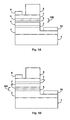
- Fig. 1A illustrates a light emitting device with a single light emitting region, according to an embodiment of the invention. The device shown in Fig. 1A is a VRCLED or VCSEL incorporating a tunnel junction as a hole spreading layer. A light emitting active region 3 separates an n-
type layer 2 and a p-type layer 4. Active region 3 may be, for example, a single light emitting layer or a multiple quantum well structure of alternating quantum well layers and barrier layers, such as a separate confinement heterostructure, described in more detail in Application Serial No. 10/033,349, titled "Indium Gallium Nitride Separate Confinement Heterostructure Light Emitting Devices," filed November 2, 2001, and incorporated herein by reference. The n-type layer may be, for example, AIGaN doped with Si; the p-type layer 4 may be, for example, AlGaN doped with Mg; and the active region may be, for example, an InGaN multiple quantum well structure. Atunnel junction 100 is formed over p-type layer 4. -
Tunnel junction 100 includes a highly doped p-type layer 5, also referred to as a p++ layer, and a highly doped n-type layer 6, also referred to as an n++ layer.P++ layer 5 may be, for example, InGaN or GaN, doped with an acceptor such as Mg or Zn to a concentration of about 1018cm-3 to about 5x1020cm-3. In some embodiments,p++ layer 5 is doped to a concentration of about 2x1020cm-3 to about 4x1020cm-3.N++ layer 6 may be, for example, InGaN or GaN, doped with an acceptor such as Si or Ge to a concentration of about 1018cm-3 to about 5x1020cm-3. In some embodiments,n++ layer 6 is doped to a concentration of about 7x1019cm-3 to about 9x1019cm-3.Tunnel junction 100 is usually very thin, forexample tunnel junction 100 may have a total thickness ranging from about 2 nm to about 100 nm, and each ofp++ layer 5 andn++ layer 6 may have a thickness ranging from about 1 nm to about 50 nm. In some embodiments, each ofp++ layer 5 andn++ layer 6 may have a thickness ranging from about 25 nm to about 35 nm.P++ layer 5 andn++ layer 6 may not necessarily be the same thickness. In one embodiment,p++ layer 5 is 15 nm of Mg-doped InGaN andn++ layer 6 is 30 nm of Si-doped GaN.P++ layer 5 andn++ layer 6 may have a graded dopant concentration. For example, a portion ofp++ layer 5 adjacent to the underlying p-layer 4 may have a dopant concentration that is graded from the dopant concentration of the underlying p-type layer to the desired dopant concentration inp++ layer 5. Similarly,n++ layer 6 may have a dopant concentration that is graded from a maximum adjacent top++ layer 5 to a minimum adjacent to n-type layer 7.Tunnel junction 100 is fabricated to be thin enough and doped enough such thattunnel junction 100 displays low series voltage drop when conducting current in reverse-biased mode. In some embodiments, the voltage drop acrosstunnel junction 100 is about 0.1 V to about 1V. - A second n-
type layer 7 is formed overtunnel junction 100. A positiveelectrical contact 9 is attached to n-type layer 7 and a negativeelectrical contact 10 is attached to n-type layer 2. The device shown in Fig. 1A is a VRCLED or a VCSEL, thus it also includes a bottom distributed Bragg reflector (DBR) 1 under n-type layer 2. DBR 1 may be a dielectric or it may be formed in-situ of III-nitride materials. A top DBR 8 is formed on n-type layer 7. As is clear to a person of skill in the art, the device shown in Fig. 1A may be fabricated as a light emitting diode, without DBRs 1 and 8. -
Tunnel junction 100 is fabricated such that when a voltage drop is applied acrosscontacts type layer 4 is forward biased,tunnel junction 100 quickly breaks down and conducts in the reverse-bias direction with a minimal voltage drop. The layers intunnel junction 100 are thin enough and doped enough that charge carriers can tunnel through them. Each of the layers intunnel junction 100 need not have the same composition, thickness, or dopant composition.Tunnel junction 100 may also include an additional layer betweenp++ layer 5 andn++ layer 6 that contains both p- and n-type dopants. -
Tunnel junction 100 acts as a hole spreading layer to distribute positive charge carriers in p-type layer 4. Carriers in n-type III-nitride material have a much longer diffusion length than carriers in p-type III-nitride material, thus current can spread more readily in an n-type layer than a p-type layer. Since current spreading on the p-side of the p-n junction occurs in n-type layer 7, the device illustrated in Fig. 1B may have better p-side current spreading than a device lacking a tunnel junction. - A single light emitting region device incorporating a tunnel junction may also be simpler to fabricate than a similar device without the tunnel junction. Since both
contacts type layers contacts - Fig. 1B illustrates an alternative embodiment of a single light emitting region device.
Tunnel junction 100 is located beneath the active region, rather than above the active region as in the embodiment shown in Fig. 1A.Tunnel junction 100 is located between n-type layer 2 and p-type layer 4. Thus, the polarity of the device in Fig. 1B is the opposite of the polarity of the device in Fig. 1A.Tunnel junction 100 of Fig. 1B also serves as a hole spreading layer by distributing positive charge carriers in p-type layer 4. - Fig. 2 illustrates an embodiment of a light emitting device with multiple light emitting regions separated by tunnel junctions. The device shown in Fig. 2 includes a
bottom contact 11, abottom DBR 12, a firstactive region 14 sandwiched between a first n-type layer 13 and a first p-type layer 15, a secondactive region 19 sandwiched between a second n-type layer 18 and a second p-type layer 20, atop DBR 21, and atop contact 22. Atunnel junction 100, including ap++ layer 16 and ann++ layer 17 separates the twoactive regions P++ layer 16 is adjacent to first p-type layer 15 andn++ layer 17 is adjacent to second n-type layer 18.Tunnel junction 100 may have the same characteristics as the tunnel junctions described above in reference to Figs. 1A and 1B. The device shown in Fig. 2 may be formed on a conducting growth substrate such as SiC, such that the substrate separatescontact 11 andDBR 12. Alternatively, layers 13-21 may be formed on an insulating substrate which is later removed.DBR 12 andcontact 11 may be attached to layer 13 by, for example, wafer bonding. The device shown in Fig. 2 is a VRCLED or VCLED. Like the embodiments illustrated in Figs. 1A and 1B, the embodiment shown in Fig. 2 can easily be fabricated as a light emitting diode by omitting DBRs 12 and 21. In order to form both contacts on the same side of the device, a portion of the semiconductor layers may be etched away to expose a ledge on n-type layer 13, on whichcontact 11 may be formed. - Though two active regions are illustrated in Fig. 2, any number of active regions may be included between
contacts active regions -
Active regions - Devices with multiple stacked active regions, such as the device shown in Fig. 2, may offer several advantages. First, when driven at the same current density as a similar device with a single active region, a multiple stacked active region device may operate at a higher voltage than a single active region device of the same area, due to the voltage drop required by the tunnel junctions separating the active regions. Operating at higher voltage may simplify the design and reduce the cost of power supplies and drivers.
- Second, when operated at the same current density as a single active region device, a multiple stacked active region device may emit more light than a single active region device, while not requiring additional area. Increasing the brightness per area may reduce the cost of fabricating the device, because less substrate area is required for each device, thus more devices may be fabricated on a single substrate wafer. Also, higher brightness for a given area may reduce simplify the design and reduce the cost of secondary optics because the cost of optics tends to increase as the area of the optic increases.
- Third, the presence of tunnel junctions separating the active regions may enhance current spreading in the device, which distributes carriers more evenly in the layers adjacent to each active region and thus permits more radiative recombinations of carriers in the active region.
- Fourth, multiple junctions may be activated by a single pair of contacts, thus mitigating electromigration problems in the contacts and the amount of space consumed by the contacts. When III-nitride devices operate at high current, metal from the contacts can migrate into the semiconductor layers and cause reliability problems in the device. In a device with multiple lateral active regions, each time an active region is added, a set of contacts must be added, thus each time an active region is added the possibility of electromigration problems increases. In contrast, in a multiple stacked active region device, the addition of an active region does not require the addition of more contacts, thus the extent of the electromigration problem for a multiple stacked active region device is the same as a single active region device with the same contact area.
- Fig. 3 illustrates an embodiment of the invention with multiple active regions and more than two contacts. Besides
contacts contact 23 is formed on a ledge etched down to p-type layer 15. Alternatively, contact 23 may be connected to one oflayers tunnel junction 100, or to n-type layer 18.Contact 23 makesactive regions contacts contacts active region 19 emits light. When current is applied betweencontacts active region 14 emits light. In addition,contact 23 allows for modulation of the relative current flow through the different active regions. The ability to increase the current flow in some layers and decrease the current flow in other layers can be used to tune the color of the aggregate spectrum. In some embodiments, all contacts are formed on the same side of the device. In such embodiments, the contacts are formed on multiple ledges, each connecting to a different layer. - In some embodiments, part of the light emitted from one or more of the active regions in a multiple stacked active region device may be converted to a different wavelength by a wavelength converting material such as, for example, a phosphor. Fig. 4 illustrates a two active region device with a
phosphor layer 35. The device shown in Fig. 4 is an LED formed on an insulatingsubstrate 30.Interconnects 32, which may be, for example, solder, wires, or any other suitable connection, connectcontacts submount 34. The device shown in Fig. 4 is a flip chip, meaning that the device is "flipped" when mounted on the submount such that light is extracted throughgrowth substrate 30.Phosphor layer 35 may be any suitable phosphor.Phosphor layer 35 may be formed for example over just the top ofsubstrate 30, over the top and sides ofsubstrate 30, or over the top and sides ofsubstrate 30 and all or a portion of the sides of the semiconductor layers (shown in Fig. 4).Phosphor layer 35 may be thin enough such that only a portion of light emitted fromactive regions phosphor 35.Phosphor layer 35 may contain scattering particles in addition to a fluorescent material. One or more phosphor layers may be used on a multiple stacked active region device to form white light. For example,active region 14 of Fig. 4 may produce blue light,active region 19 may produce cyan light, andphosphor 35 may be a doped Yttrium Aluminum Garnet (YAG) or SrS phosphor that converts some of the blue light to light having a wavelength from amber through red. The blue, cyan, and amber/red light combine to produce white light. - In another embodiment, the wavelength converting material is located between semiconductor layers, rather than applied to the surfaces of the substrate and semiconductor layers. In such an embodiment, some of the semiconductor layers are formed on a first substrate. The last layer applied over the semiconductor layers is a phosphor layer. The remaining semiconductor layers are formed on a second substrate. The second substrate is removed and the remaining semiconductor layers are wafer bonded to the phosphor layer. In still another embodiment,
growth substrate 30 is a wavelength converting material, such as single crystal YAG. - In some embodiments, more than one multiple stacked active region device may be fabricated monolithically on a single substrate. Monolithic light emitting device arrays are described in more detail in Application Serial No. 09/823,824, filed March 29, 2001, titled "Monolithic Series/Parallel LED Arrays Formed On Highly Resistive Substrates," and incorporated herein by reference.
- Fig. 5 is an exploded view of a packaged light emitting device. A heat-
sinking slug 100 is placed into an insert-moldedleadframe 106. The insert-moldedleadframe 106 is, for example, a filled plastic material molded around a metal frame that provides an electrical path.Slug 100 may include anoptional reflector cup 102. The light emitting device die 104, which may be any of the devices described above, is mounted directly or indirectly via a thermally conductingsubmount 103 to slug 100. Anoptical lens 108 may be added. - Having described the invention in detail, those skilled in the art will appreciate that, given the present disclosure, modifications may be made to the invention without departing from the spirit of the inventive concept described herein. Therefore, it is not intended that the scope of the invention be limited to the specific embodiments illustrated and described.
Claims (27)
- A III-nitride light emitting device comprising:a first layer of first conductivity type;a first layer of second conductivity type;a first active region disposed between the first layer of first conductivity type and the first layer of second conductivity type;a tunnel junction, the tunnel junction comprising:a second layer of first conductivity type having a dopant concentration greater than the first layer of first conductivity type; anda second layer of second conductivity type having a dopant concentration greater than the first layer of second conductivity type;a third layer of first conductivity type;a third layer of second conductivity type; anda second active region disposed between the third layer of first conductivity type and the third layer of second conductivity type;wherein the tunnel junction is between the first active region and the second active region.
- The device of Claim 1 wherein:the second layer of first conductivity type has a dopant concentration ranging from about 1018cm-3 to about 5x1020cm-3; andthe second layer of second conductivity type has a dopant concentration ranging from about 1018cm-3 to about 5x1020cm-3.
- The device of Claim 1 wherein the second layer of first conductivity type has a dopant concentration ranging from about 2x1020cm-3 to about 4x1020cm-3.
- The device of Claim 1 wherein the second layer of second conductivity type has a dopant concentration ranging from about 7x1019cm-3 to about 9x1019cm-3.
- The device of Claim 1 wherein the tunnel junction has a voltage drop ranging from between about 0V to about 1V when operated in reverse-biased mode.
- The device of Claim 1 wherein the tunnel junction has a voltage drop ranging from between about 0.1V to about 1V when operated in reverse-biased mode.
- The device of Claim 1 wherein:the second layer of first conductivity type has a thickness ranging from about 1 nm to about 50 nm; andthe second layer of second conductivity type has a thickness ranging from about 1 nm to about 50 nm.
- The device of Claim 1 wherein the tunnel junction has a thickness ranging from about 2 nm to about 100 nm.
- The device of Claim 1 wherein:the first active region emits light with a first peak wavelength;the second active region emits light with a second peak wavelength; and the first peak wavelength is different from the second peak wavelength.
- The device of Claim 1 wherein:the first active region emits light with a first peak wavelength;the second active region emits light with a second peak wavelength; andthe first peak wavelength is about the same as the second peak wavelength.
- The device of Claim 1 further comprising:a first contact electrically connected to the first layer of first conductivity type; anda second contact electrically connected to the third layer of second conductivity type.
- The device of Claim 11 further comprising: a third contact electrically connected to one of the first layer of second conductivity type and the third layer of first conductivity type.
- The device of Claim 11 further comprising:a submount;a first interconnect connecting the first contact to the submount; anda second interconnect connecting the second contact to the submount.
- The device of Claim 13 further comprising:a plurality of leads connected to the submount; anda lens overlying the submount.
- The device of Claim 14 further comprising a heat sink disposed between the leads and the submount.
- The device of Claim 11 wherein the second and third contacts are located on a same side of the device.
- The device of Claim 11 wherein the first, second, and third contacts are located on a same side of the device.
- The device of Claim 1 further comprising a wavelength converting material overlying the first active region.
- The device of Claim 18 wherein the wavelength converting material is a phosphor.
- The device of Claim 1 further comprising a wavelength converting material covering a top surface and a side surface of the device.
- The device of Claim 1 wherein the first active region comprises AlxInyGazN, wherein 0≤x≤ 1, 0≤y≤1, 0≤z≤1, x+y+z=1.
- The device of Claim 1 wherein the second layer of first conductivity type has a thickness less than the first layer of first conductivity type.
- The device of Claim 1 wherein the second layer of second conductivity type has a thickness less than the first layer of second conductivity type.
- The device of Claim 1 wherein the tunnel junction is between the first layer of second conductivity type and the third layer of first conductivity type.
- A method of operating a light emitting device including a first contact, a first layer of first conductivity type electrically connected to the first contact, a first active region capable of emitting light overlying the first layer of first conductivity type, a first layer of second conductivity type overlying the first active region, a tunnel junction comprising a second layer of second conductivity type and a second layer of first conductivity type overlying the first layer of second conductivity type, a third layer of first conductivity type overlying the tunnel junction, a second active region capable of emitting light overlying the third layer of first conductivity type, a third layer of second conductivity type overlying the second active region, and a second contact electrically connected to the third layer of second conductivity type, the method comprising:applying a voltage drop across the first and second contacts such that the first active region and the second active region emit light.
- A method of operating a light emitting device including a first contact, a first layer of first conductivity type electrically connected to the first contact, a first active region capable of emitting light overlying the first layer of first conductivity type, a first layer of second conductivity type overlying the first active region, a tunnel junction comprising a second layer of second conductivity type and a second layer of first conductivity type overlying the first layer of second conductivity type, a third layer of first conductivity type overlying the tunnel junction, a second active region capable of emitting light overlying the third layer of first conductivity type, a third layer of second conductivity type overlying the second active region, a second contact electrically connected to the third layer of second conductivity type, and a third contact connected to one of the tunnel junction, the first layer of second conductivity type, and the third layer of first conductivity type, the method comprising:applying a voltage drop across the first and third contacts such that the first active region emits light; andapplying a voltage drop across the second and third contacts such that the second active region emits light.
- The method of Claim 26 further comprising applying a voltage drop across the first and second contacts such that the first active region and the second active region emit light.
Applications Claiming Priority (2)
| Application Number | Priority Date | Filing Date | Title |
|---|---|---|---|
| US261534 | 1994-06-17 | ||
| US10/261,534 US6822991B2 (en) | 2002-09-30 | 2002-09-30 | Light emitting devices including tunnel junctions |
Publications (2)
| Publication Number | Publication Date |
|---|---|
| EP1403935A2 true EP1403935A2 (en) | 2004-03-31 |
| EP1403935A3 EP1403935A3 (en) | 2010-04-21 |
Family
ID=31977949
Family Applications (1)
| Application Number | Title | Priority Date | Filing Date |
|---|---|---|---|
| EP03103469A Withdrawn EP1403935A3 (en) | 2002-09-30 | 2003-09-19 | Light emitting devices including tunnel junctions |
Country Status (4)
| Country | Link |
|---|---|
| US (1) | US6822991B2 (en) |
| EP (1) | EP1403935A3 (en) |
| JP (1) | JP2004128502A (en) |
| TW (1) | TWI293806B (en) |
Cited By (18)
| Publication number | Priority date | Publication date | Assignee | Title |
|---|---|---|---|---|
| DE102004004765A1 (en) * | 2004-01-29 | 2005-09-01 | Rwe Space Solar Power Gmbh | Active Zones Semiconductor Structure |
| DE102004050891A1 (en) * | 2004-10-19 | 2006-04-20 | LumiLeds Lighting, U.S., LLC, San Jose | Group III-nitride light-emitting device, e.g. light-emitting diode, comprises active region between first layers of first and second conductivity types, tunnel junction between first and second layers of first conductive type, and contacts |
| DE102005035722A1 (en) * | 2005-07-29 | 2007-02-01 | Osram Opto Semiconductors Gmbh | Optoelectronic semiconductor chip |
| EP1793462A1 (en) * | 2005-12-05 | 2007-06-06 | Osram Opto Semiconductors GmbH | Semiconductor component and laser device |
| EP1803158A1 (en) * | 2004-10-22 | 2007-07-04 | AGILENT TECHNOLOGIES, INC. (A Delaware Corporation) | Method and structure for improved led light output |
| DE102006039369A1 (en) * | 2005-12-30 | 2007-07-05 | Osram Opto Semiconductors Gmbh | LED semiconductor for e.g. multiple coach lighting, has two radiation-generating active layers, arranged one above another in vertical direction |
| DE102006046037A1 (en) * | 2006-09-28 | 2008-04-03 | Osram Opto Semiconductors Gmbh | Light emitting diode semiconductor body for radiation-emitting component and for applications of projection, has radiation generating active layers and photonic crystal |
| DE102006046038A1 (en) * | 2006-09-28 | 2008-04-03 | Osram Opto Semiconductors Gmbh | LED semiconductor body for e.g. vehicle lighting, has radiation-generating active layers adjusted to operating voltage such that voltage dropping at series resistor is larger as voltage dropping at semiconductor body |
| DE102006057747A1 (en) * | 2006-09-27 | 2008-04-03 | Osram Opto Semiconductors Gmbh | Semiconductor body and semiconductor chip with a semiconductor body |
| DE102006051745A1 (en) * | 2006-09-28 | 2008-05-15 | Osram Opto Semiconductors Gmbh | LED semiconductor body and use of an LED semiconductor body |
| DE102007003282A1 (en) * | 2007-01-23 | 2008-07-24 | Osram Opto Semiconductors Gmbh | LED chip |
| WO2009006870A2 (en) * | 2007-07-09 | 2009-01-15 | Osram Opto Semiconductors Gmbh | Radiation-emitting semiconductor body |
| EP2071638A1 (en) * | 2006-08-08 | 2009-06-17 | "Svetlana-Optoelektronika" | Semiconductor light-emitting heterostructure |
| US7692204B2 (en) | 2003-08-29 | 2010-04-06 | Osram Gmbh | Radiation emitting semi-conductor element |
| EP1601026A3 (en) * | 2004-05-28 | 2010-11-10 | OSRAM Opto Semiconductors GmbH | Optoelectronic semiconductor device and method for its production |
| US7985964B2 (en) | 2006-05-23 | 2011-07-26 | Meijo University | Light-emitting semiconductor device |
| TWI449201B (en) * | 2004-04-07 | 2014-08-11 | Gelcore Llc | High reflectivity p-contact for ingan leds |
| US11217722B2 (en) | 2015-07-10 | 2022-01-04 | The Regents Of The University Of California | Hybrid growth method for III-nitride tunnel junction devices |
Families Citing this family (74)
| Publication number | Priority date | Publication date | Assignee | Title |
|---|---|---|---|---|
| CN1653297B (en) | 2002-05-08 | 2010-09-29 | 佛森技术公司 | High efficiency solid-state light source and methods of use and manufacture |
| US7170097B2 (en) * | 2003-02-14 | 2007-01-30 | Cree, Inc. | Inverted light emitting diode on conductive substrate |
| US20060006375A1 (en) * | 2003-04-14 | 2006-01-12 | Chen Ou | Light Mixing LED |
| JP4699681B2 (en) * | 2003-06-27 | 2011-06-15 | パナソニック株式会社 | LED module and lighting device |
| US20050041433A1 (en) * | 2003-08-18 | 2005-02-24 | Visteon Global Technologies, Inc. | Automotive lighting system |
| CN1275337C (en) * | 2003-09-17 | 2006-09-13 | 北京工大智源科技发展有限公司 | High-efficiency high-brightness multiple active district tunnel reclaimed white light light emitting diodes |
| US7524085B2 (en) | 2003-10-31 | 2009-04-28 | Phoseon Technology, Inc. | Series wiring of highly reliable light sources |
| US7819550B2 (en) | 2003-10-31 | 2010-10-26 | Phoseon Technology, Inc. | Collection optics for led array with offset hemispherical or faceted surfaces |
| WO2005091392A1 (en) | 2004-03-18 | 2005-09-29 | Phoseon Technology, Inc. | Micro-reflectors on a substrate for high-density led array |
| US7235878B2 (en) | 2004-03-18 | 2007-06-26 | Phoseon Technology, Inc. | Direct cooling of LEDs |
| EP1743384B1 (en) * | 2004-03-30 | 2015-08-05 | Phoseon Technology, Inc. | Led array having array-based led detectors |
| DK1756876T3 (en) * | 2004-04-12 | 2011-07-18 | Phoseon Technology Inc | High-density LED array |
| EP1738156A4 (en) * | 2004-04-19 | 2017-09-27 | Phoseon Technology, Inc. | Imaging semiconductor strucutures using solid state illumination |
| KR101288758B1 (en) | 2004-12-30 | 2013-07-23 | 포세온 테크날러지 인코퍼레이티드 | Methods and systems relating to light sources for use in industrial processes |
| JP5341297B2 (en) * | 2005-11-17 | 2013-11-13 | シャープ株式会社 | Compound single crystal solar cell and method for producing compound single crystal solar cell |
| KR100636542B1 (en) | 2005-07-04 | 2006-10-18 | 엘지전자 주식회사 | Light emitting device having double active layer |
| US20070029555A1 (en) * | 2005-08-04 | 2007-02-08 | Lester Steven D | Edge-emitting LED light source |
| US7560736B2 (en) * | 2005-08-15 | 2009-07-14 | General Electric Company | Mid-infrared resonant cavity light emitting diodes |
| KR100809413B1 (en) * | 2005-12-08 | 2008-03-05 | 한국전자통신연구원 | Vertical cavity surface emitting laser having monitoring photodiode and method of fabrication the same |
| US7642527B2 (en) | 2005-12-30 | 2010-01-05 | Phoseon Technology, Inc. | Multi-attribute light effects for use in curing and other applications involving photoreactions and processing |
| JP5148885B2 (en) * | 2007-01-30 | 2013-02-20 | シャープ株式会社 | Nitride semiconductor light emitting device |
| JP2008226906A (en) * | 2007-03-08 | 2008-09-25 | Sharp Corp | Nitride semiconductor light-emitting element |
| KR101393953B1 (en) * | 2007-06-25 | 2014-05-13 | 엘지이노텍 주식회사 | Light emitting device and method for manufacturing the same |
| DE102008006987A1 (en) * | 2008-01-31 | 2009-08-06 | Osram Opto Semiconductors Gmbh | Radiation receiver and method for producing a radiation receiver |
| JP2010016261A (en) * | 2008-07-04 | 2010-01-21 | Sharp Corp | Nitride semiconductor laser element |
| TWI497745B (en) * | 2008-08-06 | 2015-08-21 | Epistar Corp | Light-emitting device |
| JP2010087172A (en) * | 2008-09-30 | 2010-04-15 | Sharp Corp | Semiconductor light-emitting element and end-face emission type semiconductor laser element |
| TWI408831B (en) * | 2008-12-05 | 2013-09-11 | 私立中原大學 | Light emitting device and fabrication thereof |
| US20110220945A1 (en) * | 2010-03-09 | 2011-09-15 | Dae Sung Kang | Light emitting device and light emitting device package having the same |
| US8154052B2 (en) | 2010-05-06 | 2012-04-10 | Koninklijke Philips Electronics N.V. | Light emitting device grown on wavelength converting substrate |
| US8525148B2 (en) * | 2010-07-16 | 2013-09-03 | Micron Technology, Inc. | Solid state lighting devices without converter materials and associated methods of manufacturing |
| JP5420515B2 (en) * | 2010-10-21 | 2014-02-19 | シャープ株式会社 | Nitride semiconductor light emitting device |
| US8980728B2 (en) | 2012-01-06 | 2015-03-17 | Phostek, Inc. | Method of manufacturing a semiconductor apparatus |
| CN103199163B (en) * | 2012-01-06 | 2016-01-20 | 华夏光股份有限公司 | Light-emitting diode assembly |
| TWI466343B (en) | 2012-01-06 | 2014-12-21 | Phostek Inc | Light-emitting diode device |
| US8963297B2 (en) | 2012-01-06 | 2015-02-24 | Phostek, Inc. | Semiconductor apparatus |
| CN103296047A (en) * | 2012-03-02 | 2013-09-11 | 华夏光股份有限公司 | Light emitting diode device |
| KR20130106690A (en) * | 2012-03-20 | 2013-09-30 | 삼성전자주식회사 | White light emitting diode |
| TWI493751B (en) * | 2012-03-30 | 2015-07-21 | 華夏光股份有限公司 | Stacked bonded light emitting diode |
| TWI470826B (en) * | 2012-03-30 | 2015-01-21 | Phostek Inc | Light-emitting diode device |
| US20130264588A1 (en) * | 2012-04-09 | 2013-10-10 | Phostek, Inc. | Compact led package |
| CN103579082B (en) * | 2012-07-19 | 2016-10-12 | 华夏光股份有限公司 | The forming method of semiconductor device |
| CN104425669A (en) * | 2013-08-23 | 2015-03-18 | 上海蓝光科技有限公司 | Light-emitting diode and manufacturing method thereof |
| CN103545405B (en) * | 2013-11-11 | 2016-03-30 | 天津三安光电有限公司 | Iii-nitride light emitting devices |
| US9300112B2 (en) * | 2013-12-18 | 2016-03-29 | Lumentum Operations Llc | Packaged laser diode and method of packaging a laser diode |
| KR102320790B1 (en) * | 2014-07-25 | 2021-11-03 | 서울바이오시스 주식회사 | Uv light emitting diode and method of fabricating the same |
| KR102212561B1 (en) * | 2014-08-11 | 2021-02-08 | 삼성전자주식회사 | Semiconductor light emitting device and semiconductor light emitting device package |
| CN104465912A (en) * | 2014-08-22 | 2015-03-25 | 江苏鑫博电子科技有限公司 | LED epitaxial structure and method achieving high luminous energy density output |
| US9859470B2 (en) * | 2016-03-10 | 2018-01-02 | Epistar Corporation | Light-emitting device with adjusting element |
| US10957824B2 (en) * | 2016-04-29 | 2021-03-23 | Lumileds Llc | High luminance crisp white LED light source |
| US11211525B2 (en) | 2017-05-01 | 2021-12-28 | Ohio State Innovation Foundation | Tunnel junction ultraviolet light emitting diodes with enhanced light extraction efficiency |
| US20180331255A1 (en) * | 2017-05-12 | 2018-11-15 | X Development Llc | Fabrication of ultraviolet light emitting diode with tunnel junction |
| JP7122119B2 (en) * | 2017-05-25 | 2022-08-19 | 昭和電工光半導体株式会社 | light emitting diode |
| US10439103B2 (en) | 2017-05-25 | 2019-10-08 | Showa Denko K. K. | Light-emitting diode and method for manufacturing tunnel junction layer |
| JP7101470B2 (en) * | 2017-12-05 | 2022-07-15 | 日機装株式会社 | Nitride semiconductor light emitting device |
| US20190198709A1 (en) | 2017-12-22 | 2019-06-27 | Lumileds Llc | Iii-nitride multi-color on wafer micro-led enabled by tunnel junctions |
| JP7104519B2 (en) * | 2018-01-11 | 2022-07-21 | 日機装株式会社 | Nitride semiconductor light emitting device |
| US20220294189A1 (en) * | 2019-04-04 | 2022-09-15 | Cornell University | Monolithically inverted iii-v laser diode realized using buried tunnel junction |
| US11538962B2 (en) | 2019-04-23 | 2022-12-27 | Nichia Corporation | Light-emitting element and method for manufacturing light-emitting element |
| JP7129630B2 (en) * | 2019-04-23 | 2022-09-02 | 日亜化学工業株式会社 | Light-emitting element and method for manufacturing light-emitting element |
| US11025033B2 (en) * | 2019-05-21 | 2021-06-01 | Taiwan Semiconductor Manufacturing Co., Ltd. | Bump bonding structure to mitigate space contamination for III-V dies and CMOS dies |
| TWI781445B (en) * | 2019-09-24 | 2022-10-21 | 全新光電科技股份有限公司 | High-power vcsel |
| KR102337983B1 (en) * | 2019-11-26 | 2021-12-10 | 한국광기술원 | Light Emitting Device having Tunnel Junction and Method of Manufacturing the Same, Multi Color Device using Light Emitting Device having Tunnel Junction and Method of Manufacturing the Same |
| US11404473B2 (en) | 2019-12-23 | 2022-08-02 | Lumileds Llc | III-nitride multi-wavelength LED arrays |
| US11923398B2 (en) | 2019-12-23 | 2024-03-05 | Lumileds Llc | III-nitride multi-wavelength LED arrays |
| JP7101347B2 (en) * | 2019-12-27 | 2022-07-15 | 日亜化学工業株式会社 | Manufacturing method of light emitting element |
| JP7149486B2 (en) | 2020-04-21 | 2022-10-07 | 日亜化学工業株式会社 | Method for manufacturing light-emitting element |
| CN111564758A (en) * | 2020-05-27 | 2020-08-21 | 中国科学院半导体研究所 | Low-loss silicon-based laser |
| US11489089B2 (en) | 2020-06-19 | 2022-11-01 | Lextar Electronics Corporation | Light emitting device with two vertically-stacked light emitting cells |
| CN116097457A (en) | 2020-09-11 | 2023-05-09 | 日亚化学工业株式会社 | Nitride semiconductor element and method for manufacturing nitride semiconductor element |
| US11631786B2 (en) | 2020-11-12 | 2023-04-18 | Lumileds Llc | III-nitride multi-wavelength LED arrays with etch stop layer |
| US11476386B2 (en) | 2020-12-16 | 2022-10-18 | Lumileds Llc | Light emitting diode device |
| WO2022239330A1 (en) * | 2021-05-10 | 2022-11-17 | ソニーセミコンダクタソリューションズ株式会社 | Surface-emitting laser, surface-emitting laser array, and electronic apparatus |
| CN117134194B (en) * | 2023-10-25 | 2024-01-02 | 吉光半导体科技有限公司 | Vertical cavity surface emitting laser and preparation method thereof |
Citations (3)
| Publication number | Priority date | Publication date | Assignee | Title |
|---|---|---|---|---|
| US20010000622A1 (en) * | 1996-06-26 | 2001-05-03 | Osram Opto Semiconductors Gmbh & Co., Ohg | Light-radiating semiconductor component with a luminescence conversion element |
| WO2001033640A1 (en) * | 1999-11-03 | 2001-05-10 | Osram Opto Semiconductors Gmbh & Co. Ohg | Led white light source with broad band stimulation |
| EP1198016A2 (en) * | 2000-10-13 | 2002-04-17 | LumiLeds Lighting U.S., LLC | Stenciling phosphor layers on light emitting diodes |
Family Cites Families (14)
| Publication number | Priority date | Publication date | Assignee | Title |
|---|---|---|---|---|
| US4169997A (en) | 1977-05-06 | 1979-10-02 | Bell Telephone Laboratories, Incorporated | Lateral current confinement in junction lasers |
| USH667H (en) * | 1987-05-14 | 1989-09-05 | The United States of America as represented by the Secretaryof the Air Force | Patterned tunnel junction |
| JPH0423378A (en) * | 1990-05-14 | 1992-01-27 | Matsushita Electron Corp | Semiconductor laser |
| JPH0690063A (en) * | 1992-07-20 | 1994-03-29 | Toyota Motor Corp | Semiconductor laser |
| US5376580A (en) | 1993-03-19 | 1994-12-27 | Hewlett-Packard Company | Wafer bonding of light emitting diode layers |
| JP2973794B2 (en) | 1993-09-24 | 1999-11-08 | トヨタ自動車株式会社 | Semiconductor laser |
| JP3081094B2 (en) * | 1993-10-15 | 2000-08-28 | トヨタ自動車株式会社 | Semiconductor laser and manufacturing method thereof |
| US5892787A (en) * | 1994-10-27 | 1999-04-06 | Hewlett-Packard Company | N-drive, p-common light-emitting devices fabricated on an n-type substrate and method of making same |
| US5684309A (en) | 1996-07-11 | 1997-11-04 | North Carolina State University | Stacked quantum well aluminum indium gallium nitride light emitting diodes |
| JP3719467B2 (en) * | 1997-05-16 | 2005-11-24 | 日本オプネクスト株式会社 | Optical semiconductor device |
| US6487231B1 (en) * | 1998-04-14 | 2002-11-26 | Bandwidth 9, Inc. | Vertical cavity apparatus with tunnel junction |
| US6153894A (en) * | 1998-11-12 | 2000-11-28 | Showa Denko Kabushiki Kaisha | Group-III nitride semiconductor light-emitting device |
| DE19935998B4 (en) * | 1999-07-30 | 2007-10-18 | Osram Opto Semiconductors Gmbh | Multiple semiconductor laser structure with narrow wavelength distribution |
| JP2002232078A (en) * | 2001-02-01 | 2002-08-16 | Sanyo Electric Co Ltd | Semiconductor laser and its manufacturing method |
-
2002
- 2002-09-30 US US10/261,534 patent/US6822991B2/en not_active Expired - Lifetime
-
2003
- 2003-09-19 EP EP03103469A patent/EP1403935A3/en not_active Withdrawn
- 2003-09-29 JP JP2003337723A patent/JP2004128502A/en active Pending
- 2003-09-29 TW TW092126826A patent/TWI293806B/en not_active IP Right Cessation
Patent Citations (3)
| Publication number | Priority date | Publication date | Assignee | Title |
|---|---|---|---|---|
| US20010000622A1 (en) * | 1996-06-26 | 2001-05-03 | Osram Opto Semiconductors Gmbh & Co., Ohg | Light-radiating semiconductor component with a luminescence conversion element |
| WO2001033640A1 (en) * | 1999-11-03 | 2001-05-10 | Osram Opto Semiconductors Gmbh & Co. Ohg | Led white light source with broad band stimulation |
| EP1198016A2 (en) * | 2000-10-13 | 2002-04-17 | LumiLeds Lighting U.S., LLC | Stenciling phosphor layers on light emitting diodes |
Non-Patent Citations (5)
| Title |
|---|
| DIAGNE M ET AL: "Vertical cavity violet light emitting diode incorporating an aluminum gallium nitride distributed Bragg mirror and a tunnel junction" APPLIED PHYSICS LETTERS, AIP, AMERICAN INSTITUTE OF PHYSICS, MELVILLE, NY, US, vol. 79, no. 22, 26 November 2001 (2001-11-26), pages 3720-3722, XP012029554 ISSN: 0003-6951 * |
| JAIN F ET AL: "MONOLITHIC INTEGRATION OF RED, BLUE AND GREEN LASERS FOR SMART PROJECTION DISPLAYS" 1995 SID INTERNATIONAL SYMPOSIUM DIGEST OF TECHNICAL PAPERS. ORLANDO, MAY 23 - 25, 1995; [SID INTERNATIONAL SYMPOSIUM DIGEST OF TECHNICAL PAPERS], SANTA ANA, SID, US, vol. VOL. 26, 23 May 1995 (1995-05-23), pages 516-519, XP000657166 * |
| JEON SEONG-RAN ET AL: "Lateral current spreading in GaN-based light-emitting diodes utilizing tunnel contact junctions" APPLIED PHYSICS LETTERS, AIP, AMERICAN INSTITUTE OF PHYSICS, MELVILLE, NY, US, vol. 78, no. 21, 21 May 2001 (2001-05-21), pages 3265-3267, XP012028099 ISSN: 0003-6951 * |
| OZDEN I ET AL: "A dual-wavelength indium gallium nitride quantum well light emitting diode" APPLIED PHYSICS LETTERS, AIP, AMERICAN INSTITUTE OF PHYSICS, MELVILLE, NY, US, vol. 79, no. 16, 15 October 2001 (2001-10-15), pages 2532-2534, XP012029138 ISSN: 0003-6951 * |
| TAKEUCHI T ET AL: "GaN-based light emitting diodes with tunnel junctions" JAPANESE JOURNAL OF APPLIED PHYSICS, PART 2 (LETTERS) JAPAN SOC. APPL. PHYS JAPAN, vol. 40, no. 8B, 15 August 2001 (2001-08-15), pages L861-L863, XP002571664 ISSN: 0021-4922 * |
Cited By (38)
| Publication number | Priority date | Publication date | Assignee | Title |
|---|---|---|---|---|
| US7692204B2 (en) | 2003-08-29 | 2010-04-06 | Osram Gmbh | Radiation emitting semi-conductor element |
| DE102004004765A1 (en) * | 2004-01-29 | 2005-09-01 | Rwe Space Solar Power Gmbh | Active Zones Semiconductor Structure |
| US7692202B2 (en) | 2004-01-29 | 2010-04-06 | Azur Space Solar Power Gmbh | Semiconductor structure comprising active zones |
| TWI449201B (en) * | 2004-04-07 | 2014-08-11 | Gelcore Llc | High reflectivity p-contact for ingan leds |
| EP1601026A3 (en) * | 2004-05-28 | 2010-11-10 | OSRAM Opto Semiconductors GmbH | Optoelectronic semiconductor device and method for its production |
| DE102004050891A1 (en) * | 2004-10-19 | 2006-04-20 | LumiLeds Lighting, U.S., LLC, San Jose | Group III-nitride light-emitting device, e.g. light-emitting diode, comprises active region between first layers of first and second conductivity types, tunnel junction between first and second layers of first conductive type, and contacts |
| DE102004050891B4 (en) | 2004-10-19 | 2019-01-10 | Lumileds Holding B.V. | Light-emitting III-nitride semiconductor device |
| EP1803158A4 (en) * | 2004-10-22 | 2008-04-30 | Avago Tech Ecbu Ip Sg Pte Ltd | Method and structure for improved led light output |
| EP1803158A1 (en) * | 2004-10-22 | 2007-07-04 | AGILENT TECHNOLOGIES, INC. (A Delaware Corporation) | Method and structure for improved led light output |
| DE102005035722B9 (en) | 2005-07-29 | 2021-11-18 | OSRAM Opto Semiconductors Gesellschaft mit beschränkter Haftung | Optoelectronic semiconductor chip and method for its production |
| DE102005035722B4 (en) | 2005-07-29 | 2021-09-09 | OSRAM Opto Semiconductors Gesellschaft mit beschränkter Haftung | Optoelectronic semiconductor chip and method for its production |
| DE102005035722A1 (en) * | 2005-07-29 | 2007-02-01 | Osram Opto Semiconductors Gmbh | Optoelectronic semiconductor chip |
| US8994000B2 (en) | 2005-07-29 | 2015-03-31 | Osram Opto Semiconductors Gmbh | Optoelectronic semiconductor chip |
| EP1793462A1 (en) * | 2005-12-05 | 2007-06-06 | Osram Opto Semiconductors GmbH | Semiconductor component and laser device |
| US8254426B2 (en) | 2005-12-05 | 2012-08-28 | Osram Opto Semiconductors Gmbh | Surface emitting semiconductor component, and laser device including such component |
| DE102006039369A1 (en) * | 2005-12-30 | 2007-07-05 | Osram Opto Semiconductors Gmbh | LED semiconductor for e.g. multiple coach lighting, has two radiation-generating active layers, arranged one above another in vertical direction |
| US7932526B2 (en) | 2005-12-30 | 2011-04-26 | Osram Opto Semiconductors Gmbh | LED semiconductor body and use of an LED semiconductor body |
| GB2453464B (en) * | 2006-05-23 | 2011-08-31 | Univ Meijo | Light-emitting semiconductor device |
| US7985964B2 (en) | 2006-05-23 | 2011-07-26 | Meijo University | Light-emitting semiconductor device |
| EP2071638A4 (en) * | 2006-08-08 | 2014-07-16 | Svetlana Optoelektronika | Semiconductor light-emitting heterostructure |
| EP2071638A1 (en) * | 2006-08-08 | 2009-06-17 | "Svetlana-Optoelektronika" | Semiconductor light-emitting heterostructure |
| US7649193B2 (en) | 2006-09-27 | 2010-01-19 | Osram Opto Semiconductors Gmbh | Semiconductor body and semiconductor chip comprising a semiconductor body |
| DE102006057747B4 (en) * | 2006-09-27 | 2015-10-15 | Osram Opto Semiconductors Gmbh | Semiconductor body and semiconductor chip with a semiconductor body |
| DE102006057747A1 (en) * | 2006-09-27 | 2008-04-03 | Osram Opto Semiconductors Gmbh | Semiconductor body and semiconductor chip with a semiconductor body |
| US8115219B2 (en) | 2006-09-28 | 2012-02-14 | Osram Opto Semiconductors Gmbh | LED semiconductor body and use of an LED semiconductor body |
| DE102006046038A1 (en) * | 2006-09-28 | 2008-04-03 | Osram Opto Semiconductors Gmbh | LED semiconductor body for e.g. vehicle lighting, has radiation-generating active layers adjusted to operating voltage such that voltage dropping at series resistor is larger as voltage dropping at semiconductor body |
| US8314431B2 (en) | 2006-09-28 | 2012-11-20 | Osram Opto Semiconductors Gmbh | LED semiconductor element having increased luminance |
| DE102006051745B4 (en) | 2006-09-28 | 2024-02-08 | OSRAM Opto Semiconductors Gesellschaft mit beschränkter Haftung | LED semiconductor body and use of an LED semiconductor body |
| US8283684B2 (en) | 2006-09-28 | 2012-10-09 | Osram Opto Semiconductors Gmbh | LED semiconductor body and use of an LED semiconductor body |
| DE102006046037A1 (en) * | 2006-09-28 | 2008-04-03 | Osram Opto Semiconductors Gmbh | Light emitting diode semiconductor body for radiation-emitting component and for applications of projection, has radiation generating active layers and photonic crystal |
| DE102006051745A1 (en) * | 2006-09-28 | 2008-05-15 | Osram Opto Semiconductors Gmbh | LED semiconductor body and use of an LED semiconductor body |
| US8003974B2 (en) | 2006-09-28 | 2011-08-23 | Osram Opto Semiconductors Gmbh | LED semiconductor element having increased luminance |
| DE102007003282A1 (en) * | 2007-01-23 | 2008-07-24 | Osram Opto Semiconductors Gmbh | LED chip |
| DE102007003282B4 (en) | 2007-01-23 | 2023-12-21 | OSRAM Opto Semiconductors Gesellschaft mit beschränkter Haftung | LED chip |
| WO2009006870A2 (en) * | 2007-07-09 | 2009-01-15 | Osram Opto Semiconductors Gmbh | Radiation-emitting semiconductor body |
| WO2009006870A3 (en) * | 2007-07-09 | 2009-06-18 | Osram Opto Semiconductors Gmbh | Radiation-emitting semiconductor body |
| US8314415B2 (en) | 2007-07-09 | 2012-11-20 | Osram Opto Semiconductors Gmbh | Radiation-emitting semiconductor body |
| US11217722B2 (en) | 2015-07-10 | 2022-01-04 | The Regents Of The University Of California | Hybrid growth method for III-nitride tunnel junction devices |
Also Published As
| Publication number | Publication date |
|---|---|
| US20040066816A1 (en) | 2004-04-08 |
| US6822991B2 (en) | 2004-11-23 |
| TW200417057A (en) | 2004-09-01 |
| JP2004128502A (en) | 2004-04-22 |
| TWI293806B (en) | 2008-02-21 |
| EP1403935A3 (en) | 2010-04-21 |
Similar Documents
| Publication | Publication Date | Title |
|---|---|---|
| US6822991B2 (en) | Light emitting devices including tunnel junctions | |
| JP5992662B2 (en) | Monolithic optoelectronic semiconductor body and manufacturing method thereof | |
| US9640724B2 (en) | III-nitride light emitting device with double heterostructure light emitting region | |
| KR101356271B1 (en) | LED semiconductor body and use of an LED semiconductor body | |
| EP1589593B1 (en) | Strain-controlled III-nitride light emitting device | |
| EP1560275B1 (en) | Semiconductor light emitting devices including current spreading layers | |
| US7652304B2 (en) | Contacting scheme for large and small area semiconductor light emitting flip chip devices | |
| US11404599B2 (en) | Method of forming a p-type layer for a light emitting device | |
| JP6701385B2 (en) | Method for using remote plasma chemical vapor deposition and sputtering deposition to grow layers in light emitting devices | |
| US6835957B2 (en) | III-nitride light emitting device with p-type active layer | |
| KR102190859B1 (en) | Method of forming a p-type layer for a light emitting device | |
| JP2006147679A (en) | Integrated light emitting diode, manufacturing method thereof, display and lighting apparatus for light emitting diode | |
| KR102198693B1 (en) | Semiconductor light emitting device | |
| JP6936358B2 (en) | Methods for using remote plasma chemical vapor deposition and sputtering deposition to grow layers in light emitting devices | |
| JP2006086139A (en) | Light emitting device |
Legal Events
| Date | Code | Title | Description |
|---|---|---|---|
| PUAI | Public reference made under article 153(3) epc to a published international application that has entered the european phase |
Free format text: ORIGINAL CODE: 0009012 |
|
| AK | Designated contracting states |
Kind code of ref document: A2 Designated state(s): AT BE BG CH CY CZ DE DK EE ES FI FR GB GR HU IE IT LI LU MC NL PT RO SE SI SK TR |
|
| AX | Request for extension of the european patent |
Extension state: AL LT LV MK |
|
| PUAL | Search report despatched |
Free format text: ORIGINAL CODE: 0009013 |
|
| AK | Designated contracting states |
Kind code of ref document: A3 Designated state(s): AT BE BG CH CY CZ DE DK EE ES FI FR GB GR HU IE IT LI LU MC NL PT RO SE SI SK TR |
|
| AX | Request for extension of the european patent |
Extension state: AL LT LV MK |
|
| RIC1 | Information provided on ipc code assigned before grant |
Ipc: H01L 27/15 20060101ALI20100311BHEP Ipc: H01L 33/04 20100101AFI20100311BHEP |
|
| 17P | Request for examination filed |
Effective date: 20101021 |
|
| AKX | Designation fees paid |
Designated state(s): DE |
|
| RBV | Designated contracting states (corrected) |
Designated state(s): AT BE BG CH CY CZ DE DK EE ES FI FR GB GR HU IE IT LI LU MC NL PT RO SE SI SK TR |
|
| 17Q | First examination report despatched |
Effective date: 20101221 |
|
| STAA | Information on the status of an ep patent application or granted ep patent |
Free format text: STATUS: THE APPLICATION IS DEEMED TO BE WITHDRAWN |
|
| 18D | Application deemed to be withdrawn |
Effective date: 20110503 |