EP1396879A1 - Method of fabricating semiconductor wafer and susceptor used therefor - Google Patents
Method of fabricating semiconductor wafer and susceptor used therefor Download PDFInfo
- Publication number
- EP1396879A1 EP1396879A1 EP02730788A EP02730788A EP1396879A1 EP 1396879 A1 EP1396879 A1 EP 1396879A1 EP 02730788 A EP02730788 A EP 02730788A EP 02730788 A EP02730788 A EP 02730788A EP 1396879 A1 EP1396879 A1 EP 1396879A1
- Authority
- EP
- European Patent Office
- Prior art keywords
- wafer
- susceptor
- single crystal
- crystal silicon
- Prior art date
- Legal status (The legal status is an assumption and is not a legal conclusion. Google has not performed a legal analysis and makes no representation as to the accuracy of the status listed.)
- Granted
Links
Images

Classifications
-
- H—ELECTRICITY
- H01—ELECTRIC ELEMENTS
- H01L—SEMICONDUCTOR DEVICES NOT COVERED BY CLASS H10
- H01L21/00—Processes or apparatus adapted for the manufacture or treatment of semiconductor or solid state devices or of parts thereof
- H01L21/67—Apparatus specially adapted for handling semiconductor or electric solid state devices during manufacture or treatment thereof; Apparatus specially adapted for handling wafers during manufacture or treatment of semiconductor or electric solid state devices or components ; Apparatus not specifically provided for elsewhere
- H01L21/683—Apparatus specially adapted for handling semiconductor or electric solid state devices during manufacture or treatment thereof; Apparatus specially adapted for handling wafers during manufacture or treatment of semiconductor or electric solid state devices or components ; Apparatus not specifically provided for elsewhere for supporting or gripping
- H01L21/687—Apparatus specially adapted for handling semiconductor or electric solid state devices during manufacture or treatment thereof; Apparatus specially adapted for handling wafers during manufacture or treatment of semiconductor or electric solid state devices or components ; Apparatus not specifically provided for elsewhere for supporting or gripping using mechanical means, e.g. chucks, clamps or pinches
- H01L21/68714—Apparatus specially adapted for handling semiconductor or electric solid state devices during manufacture or treatment thereof; Apparatus specially adapted for handling wafers during manufacture or treatment of semiconductor or electric solid state devices or components ; Apparatus not specifically provided for elsewhere for supporting or gripping using mechanical means, e.g. chucks, clamps or pinches the wafers being placed on a susceptor, stage or support
- H01L21/6875—Apparatus specially adapted for handling semiconductor or electric solid state devices during manufacture or treatment thereof; Apparatus specially adapted for handling wafers during manufacture or treatment of semiconductor or electric solid state devices or components ; Apparatus not specifically provided for elsewhere for supporting or gripping using mechanical means, e.g. chucks, clamps or pinches the wafers being placed on a susceptor, stage or support characterised by a plurality of individual support members, e.g. support posts or protrusions
-
- H—ELECTRICITY
- H01—ELECTRIC ELEMENTS
- H01L—SEMICONDUCTOR DEVICES NOT COVERED BY CLASS H10
- H01L21/00—Processes or apparatus adapted for the manufacture or treatment of semiconductor or solid state devices or of parts thereof
- H01L21/67—Apparatus specially adapted for handling semiconductor or electric solid state devices during manufacture or treatment thereof; Apparatus specially adapted for handling wafers during manufacture or treatment of semiconductor or electric solid state devices or components ; Apparatus not specifically provided for elsewhere
- H01L21/67005—Apparatus not specifically provided for elsewhere
- H01L21/67011—Apparatus for manufacture or treatment
- H01L21/67098—Apparatus for thermal treatment
- H01L21/67103—Apparatus for thermal treatment mainly by conduction
Landscapes
- Engineering & Computer Science (AREA)
- Physics & Mathematics (AREA)
- Condensed Matter Physics & Semiconductors (AREA)
- General Physics & Mathematics (AREA)
- Manufacturing & Machinery (AREA)
- Computer Hardware Design (AREA)
- Microelectronics & Electronic Packaging (AREA)
- Power Engineering (AREA)
Abstract
Description
- This invention relates to a method of manufacturing a semiconductor wafer and a susceptor used therefor in which a single crystal silicon wafer is mounted on the susceptor for heat treatment to manufacture a semiconductor wafer.
- In the process for manufacturing semiconductors from single crystal silicon wafers (hereinafter, named "wafer"), various types of heat treatment are performed for the wafers by using various apparatuses. As main methods for mounting the wafers on each of the apparatuses, there are provided a first method for arranging the wafers in the apparatus in line in standing condition while supporting the periphery edge portion of each wafer and a second method for mounting the/each wafer(s) on a susceptor in the apparatus while holding the back surface side of the wafer(s). In the second method, when the heat treatment is, for example, performed for the vapor-phase epitaxial growth, a single wafer processing type, a pancake type and barrel type (or cylinder type) apparatuses are known. In the single wafer processing type apparatus, the heat treatment is performed for the wafer each time one of the wafers is mounted on the susceptor. In the pancake or barrel type apparatus, the heat treatment is simultaneously performed for a plurality of wafers arranged in line on the susceptor. In the single wafer processing type, the pancake type and the barrel type apparatuses, a circular concavity (pocket) is formed at a wafer mounting position on the susceptor. The pocket is generally made of carbon coated with silicon carbide. Diameter and depth of the pocket are designed while considering diameter and thickness of a wafer to be processed, and conditions for appropriately performing the heat treatment of the vapor-phase epitaxial growth or the like for the wafer.
- In a case where the bottom of the pocket is formed on a flat surface, when a wafer W is mounted on the susceptor, the wafer easily slides on the pocket.
- To prevent sliding of a wafer, grooves are, for example, cut in a lattice shape in the bottom surface portion of the pocket to form a large number of convexities formed in a trapezoid shape, as shown in FIG. 1A. Therefore, when a wafer is mounted on the bottom of the pocket, the wafer is held by the large number of convexities from the side of the back surface thereof.
- In the apparatus described above, before the heat treatment, a wafer is transferred from a standby position to the susceptor, on which the heat treatment is performed, by a transfer system such as a Bernoulli-chuck transfer system or the like, and the wafer is mounted in the pocket formed in the susceptor. After the heat treatment, the wafer is transferred to the standby position to be carried out to the outside of the apparatus. This series of operations are successively performed in the apparatus. After completing the series of operations, heat treatment operations for a next unprocessed wafer are started.
- Heat treatment for manufacturing a semiconductor wafer is usually performed at a high temperature atmosphere. Therefore, the pocket of the susceptor is heated to a high temperature by a high radio frequency coil, lamp or the like to heighten the wafer to a predetermined temperature.
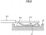
- In the apparatus described above, when the heat treatment is successively performed for the wafers, an unprocessed wafer transferred to a reaction furnace is mounted on the susceptor already heated up to a high temperature. In this case, the lower surface of the wafer is rapidly heated up at the moment when the wafer contacts with the bottom of the pocket of the susceptor. As a result, as shown in FIG. 6, the wafer is momentarily warped upward. For example, when a wafer W having a diameter of 200mm is mounted on a
susceptor 10 heated up to about 600°C, a warp momentarily occurring upward in the wafer W is observed. In this observation, a distance (amount of warp of wafer) D from one backside edge of the wafer W to the bottom of the pocket momentarily reaches about 3.2mm. - This warp momentarily occurs in the wafer W. However, when the transfer system such as the Bernoulli-chuck is, for example, placed to be close to the wafer W, the wafer W comes in contact with the transfer system at the moment when the wafer W is warped upward, and a problem is arisen that scratches are sometimes generated on a surface of the wafer W.
- An object of the present invention is to provide a method of manufacturing a semiconductor wafer and a susceptor used therefor in which warp of a single crystal silicon wafer occurring at the moment of mounting the single crystal silicon wafer on the susceptor can be lessened in the manufacturing process of the semiconductor wafer.
- According to the problem described above, the inventor of the present invention examined the transferring and mounting of the wafer W in the apparatus. As a result, as shown in FIG. 2, the inventor understood that warp of the wafer W is lessened so as to mount the wafer W in a stable condition when the intervals of convexities formed in the pocket of the susceptor are lengthened.
- When the intervals of the convexities being in contact with the wafer W on the bottom of the pocket are changed, the number of convexities per a unit area is changed, and a contact ratio of the pocket with the wafer is changed. Therefore, the inventor thought that the amount of warp of the wafer W could be lessened by adjusting the contact ratio.
- The inventor understood that, as a result of the examination, for example, when a wafer is mounted in the pocket of the susceptor set to 600°C, if the contact ratio is set to 1.1% or less, or more preferably set to 1% or less (groove width of 1.8mm or more), the amount of warp of the wafer W can be largely lessened and the generation of scratches in the wafer W can be prevented.
- However, when the intervals of the convexities are set to be larger than a certain value, because heat is not sufficiently transferred from the pocket to the wafer, slip dislocation occurs in the wafer. Therefore, the lower limit of the contact ratio of the pocket with the wafer is preferably set to 0.1% or more to suppress the occurrence of the slip dislocation.
- According to the first aspect of the present invention, a method of manufacturing a semiconductor wafer according to the present invention comprises mounting a single crystal silicon wafer in a pocket arranged in a susceptor, and performing heat treatment for the single crystal silicon wafer to manufacture the semiconductor wafer, wherein a contact ratio of the pocket with the single crystal silicon wafer is set to 0.1% or more and 1.1% or less.
- The contact ratio of the pocket with the single crystal silicon wafer can be adjusted, for example, by forming grooves in the pocket in a lattice shape so as to enlarge the width of the grooves.
- In this case, the width of each groove formed in the pocket is preferably set to 1.8mm or more.
- More preferably, the contact ratio is set to 0.1% or more and 1% or less.
- The pocket is, for example, applied to the susceptor used in the single wafer processing type apparatus, the pancake type apparatus and the barrel type apparatus which are selected from various apparatuses for performing heat treatment of the wafer such as an apparatus for performing vapor-phase epitaxial growth, a CVD apparatus and the like and are characterized by mounting a single crystal silicon wafer on the pocket while the back surface of the wafer is in contact with the pocket. Also, the grooves formed in the pocket can be formed according to machine work. Material of the susceptor is preferably carbon coated with silicon carbide, and the susceptor may be occasionally made of quartz, silicon or the like.
- In the method of manufacturing the semiconductor wafer according to the present invention, because warp of the wafer mounted on the susceptor is largely lessened, contact of the wafer with a member such as a transfer system placed close to the wafer can be prevented, and generation of scratches on the surface of the wafer due to warp of the wafer can be prevented.
- According to the second aspect of the present invention, a method of manufacturing a semiconductor wafer according to the present invention comprises mounting a single crystal silicon wafer in a pocket arranged in a susceptor, and performing heat treatment for the single crystal silicon wafer to manufacture a semiconductor wafer, wherein a contact ratio of the pocket with the single crystal silicon wafer is set to 0.1% or more and 0.3% or less when a temperature in the susceptor is about 900°C.
- According to the third aspect of the present invention, a susceptor of the present invention having a pocket for mounting a single crystal silicon wafer and used to manufacture a semiconductor wafer, wherein a contact ratio of the pocket with the single crystal silicon wafer is set to 0.1% or more and 1.1% or less.
- According to the fourth aspect of the present invention, a susceptor of the present invention having a pocket for mounting a single crystal silicon wafer and used to manufacture a semiconductor wafer, wherein a contact ratio of the pocket with the single crystal silicon wafer is set to 0.1% or more and 0.3% or less when a temperature in the susceptor is about 900°C.
-
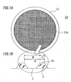
- FIG. 1A is an upper view showing the bottom of a pocket of a susceptor used for a semiconductor wafer manufacturing method according to the present invention;
- FIG. 1B is an enlarged sectional view showing the bottom of the pocket of the susceptor used for the semiconductor wafer manufacturing method according to the present invention;
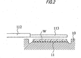
- FIG. 2 is a sectional view showing a wafer W mounted on the pocket of the susceptor in a warp lessened condition;
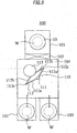
- FIG. 3 is a plane view schematically showing a single wafer processing type vapor-phase epitaxial growth apparatus as an example of an apparatus according to the present invention;
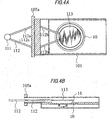
- FIG. 4A is a plane-sectional view showing a chuck arrived over the susceptor in a reaction furnace of the vapor-phase epitaxial growth apparatus of FIG. 3;
- FIG. 4B is a cross-sectional view showing a chuck arrived over the susceptor in a reaction furnace of the vapor-phase epitaxial growth apparatus of FIG. 3;
- FIG. 5A is a graph showing an amount of warp of a wafer W with respect to groove width when the wafer W is mounted in each of pockets having different contact ratios;
- FIG. 5B is a graph showing an amount of warp of a wafer W with respect to contact ratio when the wafer W is mounted in each of pockets having different contact ratios; and
- FIG. 6 is a cross-sectional view showing that a wafer transferred by the chuck of FIG. 3 is warped upward at the moment when the wafer is mounted in the pocket of the susceptor.
-
- In this embodiment, a semiconductor wafer manufacturing method for forming a single crystal thin film by performing vapor-phase epitaxial growth on a main surface of a wafer W will be described as an example of the heat treatment according to the present invention. This vapor-phase epitaxial growth is performed in a single wafer processing type vapor-
phase growth apparatus 100 shown in FIG. 3. - The vapor-
phase growth apparatus 100 comprises areaction furnace 101, load-lock chambers transfer chamber 104 placed between thereaction furnace 101 and the load-lock chambers reaction furnace 101 and thetransfer chamber 104 are partitioned by an open-closetype gate valve 105. - Each of the load-
lock chambers phase growth apparatus 100, and plurality of wafers W of before-vapor-phase-epitaxial-growth (hereinafter; named "pre-treatment") are normally mounted on a cassette (not shown) respectively along the upper-lower direction while the main surfaces of the wafers W are placed upward. The wafers W are transferred one by one to thetransfer chamber 104. After performing the vapor-phase epitaxial growth. (hereinafter, named "post-treatment") for each wafer W, the wafers W are transferred to the load-lock chamber - The
transfer chamber 104 acts as a place at which a wafer W is transferred between thereaction furnace 101 and the load-lock chambers transfer chamber 104 has ahandler 110 denoting a holding and transfer unit of the wafer W. - The
handler 110 comprises anarm 112 attached to be able to perform reciprocating and rotational movement, expand and contract in a horizontal direction around asupport point 111 which is placed almost at the center of thetransfer chamber 104, and a disc-shapedchuck 113, arranged at the end of thearm 112, for holding the wafer W. Thearm 112 comprisesfirst links second links arm 112 is expanded and contracted by moving the pairs of thelinks points links - The transfer of the single crystal silicon wafer performed by the
handler 110 is based on Bernoulli-chuck method. In detail, gas such as nitrogen or the like is strongly blown from the center of thechuck 113 to the periphery, and the wafer W is adsorbed and held by thechuck 113 without contacting to thechuck 113 in the neighborhood of the lower surface of thechuck 113 according to the Bernoulli's effect. Thearm 112 is then rotationally moved at the same time, expanded and contracted to move thechuck 113 while keeping the holding of the wafer W, and the wafer W is moved. When thechuck 113 arrives at the position at which the wafer W should be mounted in thereaction furnace 101, the gas flow of thechuck 113 is changed to release the holding of the wafer W, so that the wafer W is apart from thechuck 113 and is mounted at a predetermined position under thechuck 113. - The
reaction furnace 101 is a place at which each of the wafers W transferred by thehandler 110 is placed and vapor-phase epitaxial growth of the single crystal thin film is performed on a main surface of the wafer W. As shown in FIGS. 3, 4A and 4B, asusceptor 10 having apocket 11 is arranged in thereaction furnace 101 to mount the wafer W in thepocket 11. - As shown in FIG. 1A, a large number of
grooves 1 are formed on a bottom 11a of thepocket 11 in a lattice shape. As shown in FIG. 1B, each portion surrounded by thegrooves 1 is aconvexity 2. When a wafer W is mounted on thepocket 11, the wafer W comes in contact with theupper surface 2a of theconvexity 2. - When a ratio (%) of the total area of the
upper surfaces 2a of theconvexities 2 to the area of the bottom 11a of thepocket 11 in the unit area of thepocket 11 is defined as a contact ratio of thepocket 11 with the wafer W, the bottom 11a of thepocket 11 is formed so as to set the contact ratio to 0.1% or more and 1.1% or less, more preferably 1% or less. - In the first method for adjusting the contact ratio within the range described above, an interval A of the
convexities 2 is adjusted (by adjusting a groove width B) while fixing a size C (conveniently indicated by the length of a side of the top of the convexity in section, in FIG. 1B) of theupper surface 2a of theconvexity 2 shown in FIG. 1B, so that the number ofconvexities 2 per unit area is increased or decreased. - In the second method, the interval A of the
convexities 2 is fixed, and the size of theconvexity 2, that is, the size C of theupper surface 2a of theconvexity 2 is adjusted by adjusting the size of the groove width B. - In the third method, both the interval A (the groove width B) of the
convexities 2 and the size C of theupper surface 2a of theconvexity 2 are adjusted. - Next, a semiconductor wafer manufacturing method for performing vapor-phase epitaxial growth on a wafer W will be described with the operation of the vapor-
phase growth apparatus 100. - After a pre-treatment wafer W mounted in either of the load-
lock chambers chuck 113 is moved to arrive at a position placed over the main surface of the wafer W, and thechuck 113 holds the wafer W by ejecting a gas from thechuck 113. Thechuck 113 is then moved toward thereaction furnace 101 by expanding, contracting and rotationally moving thearm 112. After an open-close member 105a of thegate valve 105 is opened, thearm 112 is expanded to make thechuck 113 arrive at the position placed over thepocket 11 of the susceptor 10 (FIGS. 4A and 4B). The holding of the wafer W is then released, so that the wafer W is mounted in the pocket 11 (FIG. 2). - After the wafer W is mounted, the
arm 112 is contracted to return thechuck 113 to thetransfer chamber 104. The open-close member 105a of thegate valve 105 is then closed, and the vapor-phase epitaxial growth (heat treatment) for the wafer W in thereaction furnace 101 is started. - In the vapor-phase epitaxial growth, source material such as dichlorosilane, trichlorosilane or the like is supplied with a dopant gas on the main surface of the wafer W in a condition of the
reaction furnace 101 heated up to about 1100°C to 1200°C. The gas composition, the gas flow rate, the period of the gas supply and the temperature are appropriately set while considering the film thickness and the like of a desired silicon epitaxial wafer (semiconductor wafer). - After the vapor-phase epitaxial growth, the temperature in the furnace is set to a desired temperature of about 600°C to 900°C when a next pre-treatment wafer is mounted in the furnace.
- After the vapor-phase-epitaxial growth, the open-
close member 105a of thegate valve 105 is opened, and the post-treatment wafer W is transferred to one of the load-lock chambers handler 110. After the transfer, another pre-treatment wafer W from the load-lock chamber reaction furnace 101 in the same manner, and the series of epitaxial growth treatment operations are started. - As described above, after the vapor-phase epitaxial growth, the temperature in the furnace is set to the desired temperature of about 600°C to 900°C when the next pre-treatment wafer is mounted in the furnace. However, when temperature in the furnace is relatively high as described in the following examples and comparative example, the contact ratio of the pocket with the wafer is preferably made small. On the other hand, when temperature in the furnace is relatively low, even though the contact ratio is larger, sufficient effect can be obtained. It is better to appropriately select the contact ratio in the range of 0.1% to 1.1% according to the operation conditions. For example, the contact ratio is preferably set to 0.1% to 0.3% at the temperature of about 900°C.
- In the examples and comparative example described later, a semiconductor wafer manufacturing method for epitaxially growing the single crystal silicon thin film on a silicon wafer is described as an example. However, the present invention is effective to the process for forming a thin film of a distorted semiconductor layer such as SiGe or the like on a silicon wafer or other thin film forming processes.
- In this example, a vapor-phase epitaxial growth is performed as a heat treatment for a wafer W by using a single wafer processing type vapor-
phase growth apparatus 100 described in the embodiment, and a silicon epitaxial wafer denoting one type of semiconductor wafer is manufactured. - A
pocket 11 made of carbon coated with silicon carbide is formed in asusceptor 10 arranged in areaction furnace 101 of the vapor-phase growth apparatus 100. Two types ofpockets having grooves 1 formed in the lattice shape are prepared as thepockets 11 so as to set a groove width B of a bottom 11a to (1) 3.64mm (3.84mm as an interval A of convexities 2) and (2) 1.72mm (1.92mm as the interval A of convexities 2). Each wafer W is then mounted on thepocket 11 to perform vapor-phase expitaxial growth. - The
convexity 2 of eachpocket 11 is formed in a trapezoid shape on the bottom and has anupper surface 2a of almost square shape having sides of about 0.2mm. Therefore, a contact ratio of thepocket 11 with the wafer W is set to (1) 0.3% and (2) 1.1%, respectively. - Temperature in the
reaction furnace 101 and thesusceptor 10 is set to about 600°C when a wafer W is transferred. A wafer W having a diameter of 200mm is transferred by achuck 113 and is mounted on thepocket 11 of thesusceptor 10. In this embodiment, distance between thechuck 113 and the bottom 11a of the pocket 11 (distance fromupper surface 2a of theconvexity 2 to the chuck 113) is 5mm. - After mounting the wafer W in the
pocket 11, thechuck 113 is returned to atransfer chamber 104, an open-close member 105a of agate valve 105 is closed, and vapor-phase epitaxial growth is started. After the vapor-phase growth, the open-close member 105a of thegate valve 105 is opened, the wafer W formed a single crystal thin film on thesusceptor 10 is held by thehandler 110 and is transferred to the load-lock chamber 102. - The treatment was performed by using two types of
susceptors 10. The amount D of warp in the wafers W were (1) 0.01mm and (2) 0.05mm at the moment when each wafer W was mounted in thepocket 11, and no scratch was observed on the surface of each silicon epitaxial wafer manufactured according to the vapor-phase growth. - As described above, when the amount D of warp of a wafer is about 0.05mm, influence such as generation of scratches on the wafer W is hardly exerted. That is, when a pocket is formed to set the groove width B to 1.72mm or more and to set the contact ratio of the
pocket 11 with a wafer W to 1.1% or less, upward warp of the wafer W occurring at the moment of mounting the wafer W can be sufficiently prevented. - In this Comparative Example, in the same manner as in the Example 1, the
pockets 11 formed at the groove width B of (3) 1.08mm (1.28mm as the interval A of the convexities 2) and (4) 0.44mm (0.64mm as the interval A of the convexities 2) respectively are prepared. A wafer W is mounted in eachpocket 11, and vapor-phase epitaxial growth is performed for the wafer W under the same conditions as those in the Example 1. The contact ratios of the wafers W with thepockets 11 are (3) 2.4% and (4) 9.8% respectively. - In the Comparative Example, the amount D of warp of the wafers W were (3) 2.9mm and (4) 3.2mm respectively at the moment when the wafers W were mounted in the
pockets 11, so that remarkable upward warp was observed. - When a cold wafer W is mounted on the
susceptor 10 heated up to about 600°C, the wafer W jumps up about 2mm. Therefore, when vapor-phase epitaxial growth is performed by using thepocket 11 used in the Comparative Example, there is high possibility that scratches are generated on the surface of the wafer W by contacting the wafer W with thechuck 113 placed over the wafer W. - To compare a vapor-phase epitaxial growth method in the Example 1 with that in the Comparative Example, the contact ratio (%) of the pocket with the wafer W for each of the pockets (1) to (4) and the amount D of warp of the wafer W measured by using each pocket are shown in Table 1.
susceptor interval A of convexities (mm) Groove width B (mm) Contact ratio (%) amount D of warp of wafer (mm) (1) 3.84 3.64 0.3 0.01 (2) 1.92 1.72 1.1 0.05 (3) 1.28 1.08 2.4 2.9 (4) 0.64 0.44 9.8 3.2 - A graph of the amount D of warp of the wafer W with respect to each groove width B is shown in FIG. 5A, and a graph of the amount D of warp of the wafer W with respect to each contact ratio is shown in FIG. 5B.
- In FIGS. 5A and 5B, when the contact ratio is changed from 2.4% to 1.1% (the interval A of the convexities is changed from 1.28mm to 1.92mm, and the groove width B is changed from 1.08mm to 1.72mm), it is understood that the amount D of warp of the wafer W is rapidly reduced from 2.9mm to 0.05mm.
- Accordingly, when the contact ratio of the
pocket 11 with the wafer W is set to 1.1% or less, or preferably set to 1% or less (the groove width of 1.8mm or more), the amount of instantaneous warp occurring at the moment of mounting a wafer can be considerably made small, and generation of scratches due to warp can be prevented. Therefore, this method is effective for manufacturing a silicon epitaxial wafer. - In this Comparative Example, a pocket having a larger groove width B and a smaller contact ratio with a wafer W is formed in a
susceptor 10, vapor-phase epitaxial growth is performed for the wafer W under the same conditions as those in the Example 1, and a silicon epitaxial wafer is manufactured. - As a result, when the contact ratio of the
pocket 11 with the wafer W is set to be lower than 0.1% (the groove width B is larger than about 6.1mm), occurrence of slip dislocation in the wafer W is found out. - Accordingly, the contact ratio of the
pocket 11 with the wafer W is preferably set to be 0.1% or more. - In this Example, a
pocket 11 formed at the groove width B of (1) 3.64mm (3.84mm as the interval A of theconvexities 2, and the contact ratio of 0.3% with a wafer W) is prepared. Temperature of thesusceptor 10 is set to about 900°C when a wafer W is mounted in thepocket 11, vapor-phase epitaxial growth is performed for the wafer W under the same conditions as those in the Example 1, and a silicon epitaxial wafer is manufactured. - As a result, no,generation of scratches is found out on the surface of the manufactured silicon epitaxial wafer. Accordingly, when the contact ratio of the
pocket 11 with the wafer W is set to 0.3%, even though the temperature of thesusceptor 10 is set to about 900°C, the silicon epitaxial wafer can be appropriately manufactured. - In this Comparative Example, a
pocket 11 formed at the groove width B of (2) 1.72mm (1.92mm as the interval A of theconvexities 2, and the contact ratio of 1.1% with a wafer W) is used, and vapor-phase epitaxial growth is performed for the wafer W.under the same conditions as those in the Example 2. As a result, scratch(es) generated due to the contact with thechuck 113 are found out on the surface of the manufactured silicon epitaxial wafer. - Accordingly, in a case where the temperature of the
susceptor 10 mounting a wafer W exceeds 900°C, when the contact ratio of thepocket 11 with the wafer W is set to 0.3% or less, warp of the wafer can be sufficiently and appropriately suppressed. - The
grooves 1 formed at the bottom 11a of thepocket 11 are not limited to the shape shown in FIG. 1. For example, thegrooves 1 are not limited to the lattice shape. Further, it is not required that the groove width B, the intervals of thegrooves 1, the shape of eachconvexity 2, or the area of theupper surface 2a of eachconvexity 2 is uniformly set in thewhole bottom 11a. - Moreover, the groove forming method is not limited. For example, the
grooves 1 may be formed by cutting, may be formed by arranging convexities on the surface, and may be integrally formed. - As to the configuration of each apparatus performing the heat treatment for the wafer, the present invention is not limited to the configuration of the vapor-phase growth apparatus according to the embodiment, and the configuration of the vapor-phase growth apparatus can be appropriately changed.
- As described above, the
grooves 1 of the lattice shape are formed on the bottom 11a of thepocket 11 of thesusceptor 10 mounting a wafer W. The wafer W comes in contact with theupper surfaces 2a of theconvexities 2 of thepocket 11 surrounded by thegrooves 1. The amount of warp of the wafer occurring at the moment of mounting the single crystal silicon wafer on the susceptor at high temperature can be reduced by adjusting the contact ratio (contact area per unit area) of thepocket 11 with the wafer W while adjusting the intervals A of theconvexities 2, the size of theupper surfaces 2a of theconvexities 2 and/or the groove width B. - According to the present invention, upward warp of a wafer occurring at the moment of mounting the wafer on a susceptor can be considerably reduced. Further, because the contact of the wafer with a member placed close to a transferring unit or the like can be prevented by reducing warp of the wafer, the present invention is appropriate. Accordingly, the semiconductor wafer manufacturing method and the susceptor used therefor according to the present invention are particularly appropriate to manufacture a semiconductor from a single crystal silicon wafer.
Claims (10)
- A method of manufacturing a semiconductor wafer, comprising mounting a single crystal silicon wafer in a pocket arranged in a susceptor, and performing heat treatment for the single crystal silicon wafer to manufacture the semiconductor wafer,
wherein a contact ratio of the pocket with the single crystal silicon wafer is set to 0.1% or more and 1.1% or less. - The method of manufacturing the semiconductor wafer as claimed in claim 1, wherein a width of a groove formed in the pocket is set to 1.8mm or more.
- The method of manufacturing the semiconductor wafer as claimed in claim 1, wherein the contact ratio is set to 0.1% or more and 1% or less.
- The method of manufacturing the semiconductor wafer as claimed in any one of claims 1 to 3, wherein a material of the susceptor is carbon coated with silicon carbide.
- A method of manufacturing a semiconductor wafer, comprising mounting a single crystal silicon wafer in a pocket arranged in a susceptor, and performing heat treatment for the single crystal silicon wafer to manufacture the semiconductor wafer,
wherein a contact ratio of the pocket with the single crystal silicon wafer is set to 0.1% or more and 0.3% or less when a temperature in the susceptor is about 900°C. - A susceptor having a pocket for mounting a single crystal silicon wafer and used to manufacture a semiconductor wafer,
wherein a contact ratio of the pocket with the single crystal silicon wafer is set to 0.1% or more and is set to 1.1% or less. - The susceptor as claimed in claim 6, wherein a width of a groove formed in the pocket is set to 1.8mm or more.
- The susceptor as claimed in claim 6, wherein the contact ratio is set to 0.1% or more and 1% or less.
- The susceptor as claimed in any one of claims 6 to 8, wherein a material of the susceptor is carbon coated with silicon carbide.
- A susceptor having a pocket for mounting a single crystal silicon wafer and used to manufacture a semiconductor wafer,
wherein a contact ratio of the pocket with the single crystal silicon wafer is set to 0.1% or more and 0.3% or less when a temperature in the susceptor is about 900°C.
Applications Claiming Priority (3)
| Application Number | Priority Date | Filing Date | Title |
|---|---|---|---|
| JP2001165165 | 2001-05-31 | ||
| JP2001165165 | 2001-05-31 | ||
| PCT/JP2002/005276 WO2002097872A1 (en) | 2001-05-31 | 2002-05-30 | Method of fabricating semiconductor wafer and susceptor used therefor |
Publications (3)
| Publication Number | Publication Date |
|---|---|
| EP1396879A1 true EP1396879A1 (en) | 2004-03-10 |
| EP1396879A4 EP1396879A4 (en) | 2006-09-27 |
| EP1396879B1 EP1396879B1 (en) | 2008-02-20 |
Family
ID=19007871
Family Applications (1)
| Application Number | Title | Priority Date | Filing Date |
|---|---|---|---|
| EP02730788A Expired - Lifetime EP1396879B1 (en) | 2001-05-31 | 2002-05-30 | Method of fabricating semiconductor wafer |
Country Status (5)
| Country | Link |
|---|---|
| US (1) | US6890383B2 (en) |
| EP (1) | EP1396879B1 (en) |
| JP (1) | JP3900154B2 (en) |
| DE (1) | DE60225135T2 (en) |
| WO (1) | WO2002097872A1 (en) |
Cited By (1)
| Publication number | Priority date | Publication date | Assignee | Title |
|---|---|---|---|---|
| WO2020051217A1 (en) | 2018-09-06 | 2020-03-12 | Heraeus Gmsi Llc | Susceptor and method for manufacturing the same |
Families Citing this family (13)
| Publication number | Priority date | Publication date | Assignee | Title |
|---|---|---|---|---|
| US7288404B2 (en) * | 2002-04-29 | 2007-10-30 | Regents Of The University Of California | Microcantilevers for biological and chemical assays and methods of making and using thereof |
| US20050217585A1 (en) * | 2004-04-01 | 2005-10-06 | Blomiley Eric R | Substrate susceptor for receiving a substrate to be deposited upon |
| US20050217569A1 (en) * | 2004-04-01 | 2005-10-06 | Nirmal Ramaswamy | Methods of depositing an elemental silicon-comprising material over a semiconductor substrate and methods of cleaning an internal wall of a chamber |
| US20050223985A1 (en) * | 2004-04-08 | 2005-10-13 | Blomiley Eric R | Deposition apparatuses, methods of assessing the temperature of semiconductor wafer substrates within deposition apparatuses, and methods for deposition of epitaxial semiconductive material |
| US20050223993A1 (en) | 2004-04-08 | 2005-10-13 | Blomiley Eric R | Deposition apparatuses; methods for assessing alignments of substrates within deposition apparatuses; and methods for assessing thicknesses of deposited layers within deposition apparatuses |
| JP2006351865A (en) * | 2005-06-16 | 2006-12-28 | Shin Etsu Handotai Co Ltd | Susceptor, apparatus and method for vapor phase epitaxy, and epitaxial wafer |
| JP5092162B2 (en) * | 2005-07-06 | 2012-12-05 | Sumco Techxiv株式会社 | Semiconductor wafer manufacturing method and manufacturing apparatus |
| JP4910931B2 (en) * | 2007-07-27 | 2012-04-04 | 信越半導体株式会社 | Vapor growth method |
| US8021968B2 (en) | 2007-08-03 | 2011-09-20 | Shin-Etsu Handotai Co., Ltd. | Susceptor and method for manufacturing silicon epitaxial wafer |
| JP5092975B2 (en) | 2008-07-31 | 2012-12-05 | 株式会社Sumco | Epitaxial wafer manufacturing method |
| CN101916794A (en) * | 2010-06-25 | 2010-12-15 | 清华大学 | Equipment for continuously preparing CIGSeS solar cell absorption layer |
| ITBO20120153A1 (en) | 2012-03-21 | 2013-09-22 | Cefla Coop | BEAM RESTRICTION DEVICE FOR RADIOLOGICAL EQUIPMENT |
| KR20140070049A (en) * | 2012-11-30 | 2014-06-10 | 삼성디스플레이 주식회사 | Substrate supporting unit and apparatus of treating substrate having the same |
Citations (4)
| Publication number | Priority date | Publication date | Assignee | Title |
|---|---|---|---|---|
| JPH0718438A (en) * | 1993-06-17 | 1995-01-20 | Anelva Corp | Electrostatic chuck device |
| US5530616A (en) * | 1993-11-29 | 1996-06-25 | Toto Ltd. | Electrostastic chuck |
| US5583736A (en) * | 1994-11-17 | 1996-12-10 | The United States Of America As Represented By The Department Of Energy | Micromachined silicon electrostatic chuck |
| JP2000315720A (en) * | 1999-04-28 | 2000-11-14 | Ibiden Co Ltd | Semiconductor manufacturing jig made of ceramics |
Family Cites Families (9)
| Publication number | Priority date | Publication date | Assignee | Title |
|---|---|---|---|---|
| JPH02174116A (en) | 1988-12-26 | 1990-07-05 | Toshiba Ceramics Co Ltd | Susceptor |
| JP2848416B2 (en) | 1990-05-08 | 1999-01-20 | 富士通株式会社 | Vapor phase growth equipment |
| JPH05238882A (en) * | 1992-02-28 | 1993-09-17 | Toshiba Mach Co Ltd | Susceptor for vapor growth |
| US5531835A (en) | 1994-05-18 | 1996-07-02 | Applied Materials, Inc. | Patterned susceptor to reduce electrostatic force in a CVD chamber |
| US5514439A (en) * | 1994-10-14 | 1996-05-07 | Sibley; Thomas | Wafer support fixtures for rapid thermal processing |
| US5761023A (en) * | 1996-04-25 | 1998-06-02 | Applied Materials, Inc. | Substrate support with pressure zones having reduced contact area and temperature feedback |
| US6245152B1 (en) * | 1996-07-05 | 2001-06-12 | Super Silicon Crystal Research Institute Corp. | Method and apparatus for producing epitaxial wafer |
| JPH10284360A (en) * | 1997-04-02 | 1998-10-23 | Hitachi Ltd | Substrate temperature control equipment and method |
| US6634882B2 (en) * | 2000-12-22 | 2003-10-21 | Asm America, Inc. | Susceptor pocket profile to improve process performance |
-
2002
- 2002-05-30 WO PCT/JP2002/005276 patent/WO2002097872A1/en active IP Right Grant
- 2002-05-30 JP JP2003500959A patent/JP3900154B2/en not_active Expired - Fee Related
- 2002-05-30 US US10/477,918 patent/US6890383B2/en not_active Expired - Lifetime
- 2002-05-30 DE DE60225135T patent/DE60225135T2/en not_active Expired - Lifetime
- 2002-05-30 EP EP02730788A patent/EP1396879B1/en not_active Expired - Lifetime
Patent Citations (4)
| Publication number | Priority date | Publication date | Assignee | Title |
|---|---|---|---|---|
| JPH0718438A (en) * | 1993-06-17 | 1995-01-20 | Anelva Corp | Electrostatic chuck device |
| US5530616A (en) * | 1993-11-29 | 1996-06-25 | Toto Ltd. | Electrostastic chuck |
| US5583736A (en) * | 1994-11-17 | 1996-12-10 | The United States Of America As Represented By The Department Of Energy | Micromachined silicon electrostatic chuck |
| JP2000315720A (en) * | 1999-04-28 | 2000-11-14 | Ibiden Co Ltd | Semiconductor manufacturing jig made of ceramics |
Non-Patent Citations (3)
| Title |
|---|
| PATENT ABSTRACTS OF JAPAN vol. 1995, no. 04, 31 May 1995 (1995-05-31) -& JP 07 018438 A (ANELVA CORP), 20 January 1995 (1995-01-20) * |
| PATENT ABSTRACTS OF JAPAN vol. 2000, no. 14, 5 March 2001 (2001-03-05) -& JP 2000 315720 A (IBIDEN CO LTD; AMATANI SEISAKUSHO:KK), 14 November 2000 (2000-11-14) * |
| See also references of WO02097872A1 * |
Cited By (2)
| Publication number | Priority date | Publication date | Assignee | Title |
|---|---|---|---|---|
| WO2020051217A1 (en) | 2018-09-06 | 2020-03-12 | Heraeus Gmsi Llc | Susceptor and method for manufacturing the same |
| EP3626865A1 (en) | 2018-09-20 | 2020-03-25 | Heraeus GMSI LLC | Susceptor and method for manufacturing the same |
Also Published As
| Publication number | Publication date |
|---|---|
| US6890383B2 (en) | 2005-05-10 |
| EP1396879A4 (en) | 2006-09-27 |
| JPWO2002097872A1 (en) | 2004-09-16 |
| DE60225135T2 (en) | 2009-02-26 |
| EP1396879B1 (en) | 2008-02-20 |
| JP3900154B2 (en) | 2007-04-04 |
| WO2002097872A1 (en) | 2002-12-05 |
| US20040129225A1 (en) | 2004-07-08 |
| DE60225135D1 (en) | 2008-04-03 |
Similar Documents
| Publication | Publication Date | Title |
|---|---|---|
| US6890383B2 (en) | Method of manufacturing semiconductor wafer and susceptor used therefor | |
| US20190109036A1 (en) | Spring-Loaded Pins For Susceptor Assembly And Processing Methods Using Same | |
| KR100893909B1 (en) | A method of manufacturing a substrate holder | |
| EP1840243B1 (en) | Susceptor for epitaxial growth and epitaxial growth method | |
| US8999063B2 (en) | Susceptor, semiconductor manufacturing apparatus, and semiconductor manufacturing method | |
| US7163393B2 (en) | Heat treatment jig for semiconductor silicon substrate | |
| JP5133298B2 (en) | Vapor growth apparatus and vapor growth method | |
| CN1682360B (en) | Heat treatment device, process for fabricating semiconductor device and process for producing substrate | |
| US20110259879A1 (en) | Multi-Zone Induction Heating for Improved Temperature Uniformity in MOCVD and HVPE Chambers | |
| CN107924821B (en) | Epitaxial growth apparatus, method for manufacturing epitaxial wafer, and lift pin for epitaxial growth apparatus | |
| JP2007251078A (en) | Vapor phase epitaxial growth device | |
| KR100975717B1 (en) | Vapor phase growing apparatus and vapor phase growing method | |
| US20200181798A1 (en) | Susceptor and chemical vapor deposition apparatus | |
| JP7316379B2 (en) | Method and apparatus for backside physical vapor deposition | |
| JP4196542B2 (en) | Vapor growth susceptor and vapor growth method using the same | |
| TW202012679A (en) | Method of manufacturing epitaxial silicon wafers | |
| JP5306432B2 (en) | Vapor growth method | |
| US20050176252A1 (en) | Two-stage load for processing both sides of a wafer | |
| JP2006237625A (en) | Heat treatment device, method for manufacturing semiconductor device and method for manufacturing substrate | |
| US20160115622A1 (en) | Vapor phase growth apparatus and vapor phase growth method | |
| US20210066113A1 (en) | Susceptor, cvd apparatus, and method for manufacturing epitaxial wafer | |
| KR20150098562A (en) | Vapor phase growing method | |
| KR20100127681A (en) | A susceptor in epitaxial wafer manufacturing apparatus | |
| CN107316824B (en) | Semiconductor integrated processing apparatus and semiconductor processing method | |
| JP2022083011A (en) | Susceptor and cvd equipment |
Legal Events
| Date | Code | Title | Description |
|---|---|---|---|
| PUAI | Public reference made under article 153(3) epc to a published international application that has entered the european phase |
Free format text: ORIGINAL CODE: 0009012 |
|
| 17P | Request for examination filed |
Effective date: 20031222 |
|
| AK | Designated contracting states |
Kind code of ref document: A1 Designated state(s): AT BE CH CY DE DK ES FI FR GB GR IE IT LI LU MC NL PT SE TR |
|
| A4 | Supplementary search report drawn up and despatched |
Effective date: 20060830 |
|
| 17Q | First examination report despatched |
Effective date: 20061208 |
|
| GRAP | Despatch of communication of intention to grant a patent |
Free format text: ORIGINAL CODE: EPIDOSNIGR1 |
|
| RTI1 | Title (correction) |
Free format text: METHOD OF FABRICATING SEMICONDUCTOR WAFER |
|
| GRAS | Grant fee paid |
Free format text: ORIGINAL CODE: EPIDOSNIGR3 |
|
| GRAA | (expected) grant |
Free format text: ORIGINAL CODE: 0009210 |
|
| AK | Designated contracting states |
Kind code of ref document: B1 Designated state(s): DE GB NL |
|
| RBV | Designated contracting states (corrected) |
Designated state(s): DE GB NL |
|
| REG | Reference to a national code |
Ref country code: GB Ref legal event code: FG4D |
|
| REF | Corresponds to: |
Ref document number: 60225135 Country of ref document: DE Date of ref document: 20080403 Kind code of ref document: P |
|
| PLBE | No opposition filed within time limit |
Free format text: ORIGINAL CODE: 0009261 |
|
| STAA | Information on the status of an ep patent application or granted ep patent |
Free format text: STATUS: NO OPPOSITION FILED WITHIN TIME LIMIT |
|
| 26N | No opposition filed |
Effective date: 20081121 |
|
| GBPC | Gb: european patent ceased through non-payment of renewal fee |
Effective date: 20080530 |
|
| PG25 | Lapsed in a contracting state [announced via postgrant information from national office to epo] |
Ref country code: GB Free format text: LAPSE BECAUSE OF NON-PAYMENT OF DUE FEES Effective date: 20080530 |
|
| PGFP | Annual fee paid to national office [announced via postgrant information from national office to epo] |
Ref country code: DE Payment date: 20210505 Year of fee payment: 20 |
|
| PGFP | Annual fee paid to national office [announced via postgrant information from national office to epo] |
Ref country code: NL Payment date: 20210415 Year of fee payment: 20 |
|
| REG | Reference to a national code |
Ref country code: DE Ref legal event code: R071 Ref document number: 60225135 Country of ref document: DE |
|
| REG | Reference to a national code |
Ref country code: NL Ref legal event code: MK Effective date: 20220529 |