EP1319963B1 - Method and device for reading out stored data from a storage phosphor - Google Patents
Method and device for reading out stored data from a storage phosphor Download PDFInfo
- Publication number
- EP1319963B1 EP1319963B1 EP01129929A EP01129929A EP1319963B1 EP 1319963 B1 EP1319963 B1 EP 1319963B1 EP 01129929 A EP01129929 A EP 01129929A EP 01129929 A EP01129929 A EP 01129929A EP 1319963 B1 EP1319963 B1 EP 1319963B1
- Authority
- EP
- European Patent Office
- Prior art keywords
- radiation
- storage phosphor
- pdn
- emission radiation
- amount
- Prior art date
- Legal status (The legal status is an assumption and is not a legal conclusion. Google has not performed a legal analysis and makes no representation as to the accuracy of the status listed.)
- Expired - Lifetime
Links
Images


Classifications
-
- G—PHYSICS
- G01—MEASURING; TESTING
- G01T—MEASUREMENT OF NUCLEAR OR X-RADIATION
- G01T1/00—Measuring X-radiation, gamma radiation, corpuscular radiation, or cosmic radiation
- G01T1/16—Measuring radiation intensity
- G01T1/20—Measuring radiation intensity with scintillation detectors
- G01T1/2012—Measuring radiation intensity with scintillation detectors using stimulable phosphors, e.g. stimulable phosphor sheets
- G01T1/2014—Reading out of stimulable sheets, e.g. latent image
Definitions
- the present invention relates to an apparatus and a method for reading out information stored in a storage phosphor according to the preambles of claims 1 and 4 or 23 and 24.
- an image is generated by an object, for example a patient, by means of X-ray radiation, which image is stored in a storage phosphor as a latent image.
- the storage phosphor is excited by means of a radiation source.
- the storage phosphor then emits, as a result of this excitation, light having an intensity that is proportional to the amount of x-ray radiation stored in the storage phosphor.
- the light emitted by the storage phosphor light is received by a detection means and then converted into electrical signals, so that the stored in the storage phosphor X-ray image can then be made visible.
- the X-ray image for example, can be displayed directly on a monitor or written on a photographic X-ray film.
- the storage phosphor provides a high dynamic range for the caching of x-ray information.
- this dynamic range can be limited by the type of detection means used to read the X-ray information from the storage phosphor. This becomes noticeable in particular when different objects are to be examined, for which very different sized x-ray doses are required.
- An apparatus for reading information stored in a storage phosphor is, for example, from the patent application WO 99/28765 known.
- the storage phosphor is excited line by line by an excitation radiation, which is generated by a radiation source.
- the radiation source may be, for example, a laser diode array.
- the light emitted due to the excitation from the storage phosphor is received by a detection means.
- this detection means on a plurality of radiation-sensitive surfaces, which are arranged in a row next to each other.
- the radiation emitted by the storage phosphor is received by the radiation sensitive surfaces.
- the detection means may be a charge coupled device (CCD) line containing a plurality of line by line photodetectors arranged side by side.
- CCD charge coupled device
- the radiation source and the detection means are guided over the storage phosphor at a uniform speed.
- a corresponding number of electrons are generated by the detection means.
- Such charges generated for the pixels of a line thus represent a measure of the amount of emission radiation emitted by the pixels of a read-out line of the storage phosphor.
- EP 1 130 417 A1 It is known to set the integration time of the detector pixels as a whole or individually.
- US 4,851,678 describes a method in which read-out parameters for reading a storage phosphor plate be set based on a previous sample reading of the storage phosphor plate.
- the present invention is based on the object of a good quality in the reproduction of information stored in a storage phosphor NEN different types, especially different doses to ensure.
- the integration time during which the radiation-sensitive areas of the detection means receive emission radiation can be adjusted.
- a common electrical signal with an indication of the quantity of emission radiation received by the interconnected areas is generated for the interconnected radiation-sensitive areas.
- the setting of the integration time or the interconnection of radiation-sensitive surfaces is carried out according to the invention as a function of a quantity of emission radiation that was previously received by the detection means.
- the dynamic range of the detection means is advantageously possible to adapt the dynamic range of the detection means to the amount of information stored in the storage phosphor. This makes better use of the available dynamic range of the detection means and the storage phosphor causes.
- By adjusting the integration time or interconnecting a plurality of radiation-sensitive areas in particular an effective pixel area which serves to receive emission radiation can be set. Short integration time or non-interconnection of radiation-sensitive areas causes a small effective pixel area, and setting a long integration time or interconnecting radiation-sensitive areas causes a large effective pixel area.
- the influence of noise sources, in particular of the detection means, on the readout result can be reduced.
- the selection quality increases.
- a special readout noise occurs.
- the readout noise may in particular result from the amplifier of the output stage of the CCD. Since, according to the invention, the emission radiation detected by a plurality of the radiation-sensitive areas is combined, the fraction of the detected useful information increases relative to the proportion of the noise in the overall signal which is generated by the combined radiation-sensitive areas.
- the amount of emission radiation to be detected is low, it is advantageous to set a longer integration time or to interconnect a plurality of the radiation-sensitive areas. If, on the other hand, a lot of information is stored in the storage phosphor, the amount of emission radiation emitted by the storage phosphor is also large. The proportion of the payload versus the amount of noise is therefore large in the overall signal. The noise, in particular of the detection means, is then negligible. In this case, a short integration time can be set or the interconnection of the radiation-sensitive areas can be dispensed with. Furthermore, due to the inventive design of the control means oversteer of the detection means can be largely avoided, so that the loss of information read at least be reduced can.
- the control means includes a first threshold, which corresponds to a certain first amount of emission radiation. With this first threshold value, the control means specifies at which quantity of previously received emission radiation a specific integration time should be set or a specific number N 1 of radiation-sensitive areas should be interconnected.
- the achievement or failure of this first threshold in receiving emission radiation by the detection means is a criterion for the control means, which serves to set the integration time or to interconnect the radiation-sensitive surfaces.
- a short integration time is set or a small, second number N 2 of radiation-sensitive areas is interconnected.
- the control means adjusts a second integration time which is greater than the first integration time or combines the first number N 1 of radiation-sensitive areas which is greater than the second number N 2 of radiation-sensitive areas.
- a type of hysteresis is set when setting the integration time or when interconnecting the radiation-sensitive surfaces.
- the control means includes a second threshold value which corresponds to a certain second quantity of emission radiation, which is smaller than the first quantity of emission radiation. This makes it possible to prevent a constant change of the set integration time or the number of interconnected radiation-sensitive areas when receiving emission radiation which moves in the region of the first threshold value.
- setting the first threshold should be advantageously ensured that overriding of the detection means is prevented.
- the criteria as to when and how to set a particular integration time, or to interconnect a certain number of radiation-sensitive areas can be determined in various ways.
- the relative difference between the emitted emissions from one or more pixels (n) can be utilized.
- the difference between the emission emissions of one or more lines output from two or more adjacent pixels of the storage phosphor can be used for the adjustment of the integration time or the interconnection of the radiation-sensitive surfaces.
- the radiation-sensitive surfaces of the detection means are configured asymmetrically.
- the quantity of emission radiation received by the detection means can be increased transversely to the direction of the line, compared to a symmetrical configuration. In this way, an improved signal-to-noise ratio is achieved in receiving the information.
- emission radiation emitted by the storage phosphor is detected immediately after the information in the storage phosphor has been stored.
- a spontaneous emission of emission radiation takes place directly after this storage, without the storage phosphor for Emitting emission radiation would have to be stimulated.
- This emitted immediately after storing the information emission radiation is therefore advantageously not lost.
- the detection of this radiation may be used by the control means to adjust the integration time or the interconnection of radiation sensitive areas. As a result, a prediction with regard to the amount of emission radiation output by the storage phosphor when it is read out can already take place. This prediction can be used primarily for presetting the control means.
- the detection of this emission radiation emitted spontaneously after the storage can be effected by automatically transporting the detection means via the storage phosphor immediately after the storage.
- the device according to the invention can be transmitted from this source a message about the storage of the information. This message can then be used directly for transporting the detection means.
- control means sets the short first integration time already before the read-out of the storage phosphor or switches the small second number N 2 of radiation-sensitive areas together.
- overriding of the detection means can already be prevented from the beginning of reading the storage phosphor.
- Fig. 1 shows a perspective view of an X-ray cassette 1, which has a read-out device according to the present invention in the form of a read head 10.
- the X-ray cassette 1 contains a storage phosphor 15, which is designed here as a phosphor plate and contains an approximately 300 micron thick layer of phosphor material. This phosphor material can be put into an excited state by X-ray irradiation. As a result, an X-ray image of an object is stored in the phosphor plate 15.
- the phosphor plate 15 is stimulable by irradiating with an excitation radiation, which is in particular in the red wavelength range, so that it emits an emission radiation, which lies in particular in the blue or ultraviolet wavelength range.
- the amount (intensity) of emission radiation emitted by the stimulated phosphor plate 15 is a measure of the previously recorded amount of X-radiation.
- the phosphor plate 15 represents a Lambert radiator. Such a Lambert radiator emits radiation in all directions.
- the read head 10 includes a radiation source for outputting the excitation radiation used to stimulate the phosphor plate 15. Furthermore, the reading head 10 contains a detection means for receiving the emission radiation output from the phosphor plate 15. The radiation source and the detection means are firmly connected to one another in the reading head 10. The read head 10 extends over the entire width of the phosphor plate 15.
- the read head 10 By means of the read head 10, the information stored in a row of the phosphor plate 15 information can be read out simultaneously.
- the line extends substantially over the entire width of the phosphor plate 15.
- the reference numeral B is in the Fig. 1 the row direction specified.
- the read head 10 is characterized by a in the Fig. 1 not shown drive transversely to the direction of the line, ie in the longitudinal direction of the phosphor plate 15, along the direction of the arrow by the reference A movable. A therefore indicates the feed direction of the reading head 10 transversely to the direction of the line.
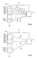
- Fig. 2 shows a section through the read head 10 transverse to the line direction B.
- the Fig. 2 shows inside the read head 10, a radiation source 11 for exciting a line of the phosphor plate 15.
- the radiation source 11 is here a laser diode array.
- the laser diode array 11 is aligned with the phosphor plate 15 in such a way that the radiation emitted by the individual laser diodes strikes the phosphor plate 15 directly.
- an optical system can be provided which serves to focus the excitation radiation emitted by the laser diode array 11.
- Fig. 2 further shows a detection means 12 for receiving the emission radiation outputted from the phosphor plate 15 during an integration time.
- the detection means 12 is formed as a CCD line.
- the CCD line 12 contains a multiplicity of photodetectors arranged side by side in parallel with light-sensitive areas 18 in one row.
- the CCD line 12 performs a photoelectric conversion of the received light radiation.
- an imaging means 14 is arranged between the phosphor plate 15 and the CCD line 12.
- This imaging means 14 is for imaging the radiation emitted from the stimulated line of the phosphor panel 15 onto the photosensitive surfaces 18 of the CCD array 12.
- a plurality of line-like microlenses may be used.
- the emission radiation emitted by the phosphor plate 15 due to the excitation by means of the excitation radiation 16 is in the Fig. 2 provided with the reference numeral 17.
- the CCD line 12 is connected at its output to a control means 13.
- This control means 13 has, inter alia, the task generated by the CCD line 12 electrical signals that contain an image of the image information stored in the phosphor plate 15, evaluate and prepare.
- the feed of the reading head 10 is controlled via the phosphor plate 15.
- a drive means 19 which may be, for example, a linear motor with which the reading head 10 is transported via the phosphor plate 15 at a uniform speed. This can be done line by line reading the phosphor plate 15.
- the reading head 10 may be mounted, for example, on plain bearings, which are mounted along the longitudinal sides of the phosphor plate 15.
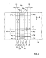
- Fig. 3 shows a further view of the reading head 10 according to the embodiment according to Fig. 2
- the Fig. 3 shows a plan view of the read head 10 and the phosphor plate 15. It is a section through the laser diode array 11 and the CCD line 12 parallel to the phosphor plate 15 and the feed direction A of the read head 10 is shown.
- the Fig. 3 shows a plurality of juxtaposed in a row laser diodes LD1 to LDn.
- the laser diodes LD1 to LDn By means of the laser diodes LD1 to LDn, the entire width of the rectangular phosphor plate 15, in which information can be stored, are excited to blast. It is possible, at least partially, to superimpose the laser radiation emitted by the laser diodes via corresponding optics so as to be able to excite the entire width of the line even with a few laser diodes.
- the Fig. 3 shows the photosensitive areas 18 of the CCD line 12 (FIG. Fig. 2 ).
- the CCD line contains photodetectors PD1 to PDn.
- Each photodetector PD1 to PDn has a photosensitive surface.
- the photosensitive surfaces 18 of the photodetectors PD1 to PDn are designed to be asymmetrical.
- the individual photosensitive surfaces 18 of the photodetectors PD1 to PDn are configured rectangular in this case. But you can also z. B. be elliptical.
- the individual photodetectors PD1 to PDn have light-sensitive areas with an extent Y CCD and in the feed direction A, ie transversely to the row direction B, with an extension X CCD .
- Y CCD is smaller than X CCD .
- the extent of the respective photosensitive surfaces 18 transverse to the direction B of the line is two to eight times as large as the extension in the direction B of the line.
- the extent Y CCD here is about 50 ⁇ m and the extent X CCD is about 400 ⁇ m. This expansion X CCD of about 400 microns is particularly advantageous because this measure can achieve a very good ratio of information collected to CCD noise.
- the irradiation of the phosphor plate 15 with X-radiation produced storage centers within the phosphor in which the information to be read is stored. Due to the excitation by the laser diode array 11, a multiplicity of adjacent scattering circles are generated in the phosphor plate 15, from which radiation is emitted on the surface of the phosphor plate 15. Each scattering circle is dependent on the particular type of phosphor plate, in particular on the grain size, the phosphor particles or the layer thickness of the phosphor used for the phosphor plate 15. The scattering circles arise because the excitation radiation emitted by the light-emitting diode line 11 is scattered within the phosphor plate 15 due to the specific nature of the phosphor used.
- the radiation emitted by the various storage centers due to the excitation radiation is also scattered within its path from the storage center to the outer surface of the phosphor panel 15. Because of these variations, blurring occurs when the information stored in the phosphor plate 15 is read out. This blur is specific to the type of phosphor used. This blurring indicates that the information contained at one point of the phosphor plate 15 does not exit exactly above this point on the surface of the phosphor plate 15. Rather, this information, which is assigned to a specific point of the phosphor plate 15, occurs somewhere within the scatter circle assigned to this point on the surface of the phosphor plate 15. As in the present read-out device, one line of the phosphor plate 15 simultaneously is excited, there is a partial overlay of the scattering circles.
- the Fig. 4 shows the schematic representation of a transmission of electrical signals 20-26 of those already in the Fig. 3 shown photodetectors PD1-PDn to the control means 13.
- the control means 13 is connected via a connection line 27 with the photodetectors PD1-PDn. Via this connecting line 27, the control means 13 can drive the photodetectors.
- the control means 13 may be, for example, a suitably programmed digital signal processor.
- the control means 13 serves to set the integration times during which the photodetectors PD1-PDn can detect emission radiation. The specification of this integration time can be passed on, for example, from the control means 13 via the connecting line 27 to the photodetectors.
- Fig. 4 shows the schematic representation of a transmission of electrical signals 20-26 of those already in the Fig. 3 shown photodetectors PD1-PDn to the control means 13.
- the control means 13 is connected via a connection line 27 with the photodetectors PD1-PDn. Via this connecting line 27, the control means 13
- FIGS Fig. 4 the electrical signals 20-26 shown.
- the first photodetector PD1 transmits the first electrical signal 20
- the second photodetector PD2 transmits the second signal 21
- the third photodetector PD3 the third electrical signal 22
- the fourth photodetector PD4 the fourth electrical signal 23
- the fifth photodetector PD5 the fifth electrical signal 24
- the penultimate photodetector PDn-1 the sixth electrical signal 25 and the last photodetector PDn, the seventh electrical signal 26 to the control means 13.
- the electrical signals 20-26 contain information about the amount of received from the individual photodetectors PD1-PDn during the set integration time Quantities of emission radiation emitted by the phosphor plate 15 due the excitation was output by the laser diodes.
- the control means 13 evaluates the information transmitted by the electrical signals and, on the basis of predetermined criteria, determines the integration time with which the individual photodetectors PD1-PDn are to receive emission radiation in the further course of the readout of the phosphor plate 15.
- the integration time for a subsequent line which still has to be read out can be determined. This subsequent line does not necessarily have to be the line immediately following.
- a prediction can be made for the emission radiation emitted by the second or third subsequent row. In the embodiment according to the Fig. 4 there was no interconnection of photodetectors. The number N of interconnected photodetectors is therefore 1 in this case.
- the control means 13 information about the amount of emission radiation received by the photodetectors PD1-PDn during the set integration time from the individual photodetectors PD1-PDn with the transmitted electrical signals 20-26.
- the signals 20-26 ie here the signals 20, 21 and 23, etc.
- Fig. 5 shows a schematic representation of another transmission of electrical signals from the photodetectors PD1-PDn to the control means 13.
- this Embodiment was due to the driving of the individual photodetectors PD1-PDn via the connecting line 27 by the control means 13 causes an interconnection of three photodetectors.
- the photodetectors PD1-PD3, the photodetectors PD4-PD6, ..., and PD (n-2) -PDn are connected together.
- the interconnected photodetectors collect emission radiation emitted by the phosphor plate 15 during the predetermined integration time.
- the amount of emission radiation received by each of three photodetectors is transmitted to the control means 13 by means of an electrical signal.
- the photodetectors PD1-PD3 transmit the electrical signal 28, the photodetectors PD4-PD6 the electrical signal 29 and the photodetectors PD (n-2) -PDn the electrical signal 30 to the control means 13. Due to the interconnection of three photodetectors the thus obtained, interconnected (effective) pixel length, with which the three photodetectors collectively detect emission radiation, viewed in the row direction B, triples. Therefore, if the extension of a photodetector in the row direction B is 50 ⁇ m, the extension of three interconnected photodetectors is 150 ⁇ m.
- the effective pixel length in the feed direction A depends on the feed rate of the read head over the phosphor plate 15 and the selected integration time.
- the (useful) signal-to-noise ratio of the electrical signals 28-30 is compared to the (useful) signal-to-noise ratio of the electrical signals 20-26 (FIG. Fig. 4 ) improved.
- the readout noise which is caused in particular by the noise of the amplifier of the CCD chip, occurs only once.
- the three useful signals generated by the three photodetectors are combined.
- the (useful) signal-to-noise ratio is increased over the non-interconnection of the photodetectors.
- Fig. 6 shows the schematic representation of a portion of the phosphor plate 15, were read out of the six lines Z1-Z6 by means of the reading head 13.
- the respective extent of the lines Z1-Z6 in the feed direction A results from the respectively set integration time when reading the lines Z1-Z6 and the feed rate of the reading head 10 during transport of the reading head 10 via the phosphor plate 15.
- the lines Z1-Z4 have an extension X1 in the feed direction A. Since the feed rate of the read head 10 remains substantially constant during readout of the entire phosphor plate 15, an integration time T1 was set by the control means 13 when the lines Z1-Z4 were read.
- the lines Z5 and Z6 have an extent X2 in the feed direction A of the read head 10.
- This extent X2 is greater than the extent X1 of the lines Z1-Z4. This means that with the feed rate of the read head 10 remaining the same, the integration time T2 for the respective readout of the lines Z5 and Z6 has been longer than the integration time T1 for the respective readout of the lines Z1-Z4. The effective pixel extent is thus greater for lines Z5 and Z6 than for lines Z1-Z4.
- the rows Z1-Z6 each have a certain number of pixels.
- Lines Z1, Z2, Z5 and Z6 each contain m pixels.
- the first row Z1 contains the pixels P11-P1m
- the second row contains the pixels P21-P2m
- the fifth row Z5 contains the pixels P51-P5m
- the sixth row Z6 contains the pixels P61-P6m.
- the pixels of the rows Z1, Z2, Z5 and Z6 each have an extension Y2 in the row direction B.
- the rows Z3 and Z4 contain n pixels.
- the third row Z3 contains the pixels P31-P3n and the fourth row Z4 contains the pixels P41-P4n.
- the pixels of the rows Z3 and Z4 each have an extent Y1 in the row direction B.
- Y1 is smaller than the extent Y2.
- the effective pixel size Y1 of the pixels of the rows Z3 and Z4 substantially corresponds to the extent Y CCD of the photodetectors PD1-PDn of the read head 10.
- the individual photodetectors were not interconnected.
- Each photodetector has transmitted its own electrical signal to the control means 13, with which the amount of emission radiation received by it has been transmitted. Since the photodetectors PD1-PDn were not connected when the lines Z3 and Z4 were read out, the lines Z3 and Z4 each have n pixels corresponding to the number of photodetectors.
- the extent Y2 in the line direction B is greater than in the lines Z3 and Z4.
- the effective pixel extent Y2 in the row direction B is therefore approximately three times as large as the extent Y1 of the pixels of the rows Z3 and Z4. Since three of the photodetectors PD1-Pdn were connected together when the lines Z1, Z2, Z5 and Z6 were read, the number m of the pixels of these lines is only one third of the number n of the pixels of the lines Z3 and Z4.
- the setting of the integration time T1 and the non-interconnection of the Photo detectors when reading the line Z3 on the basis of output from the lines Z1 and / or Z2 and received by the photodetectors emission radiations done. Due to the evaluation of the different Pixels of the lines Z1 and / or Z2 output and received by the photodetectors in the read-out of these lines Z1 and Z2 emission radiations was found, for example, that for the line Z3, a higher output emission radiation is expected.
- the interconnection of the photodetectors for the readout of the line Z3 has been reversed by the control means 13 when the lines Z1 and Z2 are read out.
- the integration time has been extended compared to the reading of lines Z1-Z4.
- This can be z. B. based on the fact that when reading the lines Z3 and / or Z4 could be predicted on the basis of the detected emission radiation that when reading the line Z5 a much smaller amount of emission radiation will be received.
- Adjusting the integration time or deciding whether and how many of the photodetectors are interconnected may be due to different criteria. These can be selected differently depending on the application.
- one or more previously read line (s) can be taken into account.
- one or more, in particular all pixels of the previously read lines can be taken into account by the control means 13.
- differences in emitting emission radiations from adjacent pixels of one or more lines are a suitable criterion for adjusting the integration time and / or the interconnection of photodetectors.
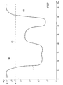
- Fig. 7 shows a first example of a series of measurements K, which is intended to illustrate the operation of the invention further.
- a slightly increased number of electrons were generated by the detection means 12.
- the number of electrons is about 8x10 4 .
- the number of generated electrons continues to decrease very much.
- the number of electrons generated is only 8x10 2 , etc.
- the remaining data can be obtained from the Fig. 7 remove.
- a first threshold S1 denoted by a number of electrons of 4x10 5 .
- This first threshold S1 serves the control means 13 to set a first, short integration time or a second, long integration time.
- a first mode M1 which in the Fig. 7 is shown above the first threshold S1, the first, short integration time is set.
- the number of electrons generated by the detection means 12 is above the first threshold value S1.
- a second mode M2 which is below the first threshold value S1 and in which the second, longer integration time is set by means of the control means 13, in each case a number of electrons are generated by the detection means 12, which lies below the first threshold S1.
- Is therefore z.
- a particular pixel of the preceding line is used as the criterion for setting the integration time for one of the lines, the result according to the exemplary embodiment of FIG Fig. 7 in that when reading out the pixel of the line 6, a number of electrons has been generated which lies above the threshold S1.
- the first, short integration time is set.
- the integration time is set to the second, longer integration time. This second integration time remains until the emission radiation is detected of the pixel of line 36. Upon detecting this emission radiation, a number of electrons is again detected, which is above the threshold value S1.
- the control means 13 therefore sets for the reading of the pixel of the line 37, the first, short integration time.
- Fig. 7 shows the setting of the integration time in the presence of a threshold value S1.
- the same procedure described here for adjusting the integration time can also be used for interconnecting the photodetectors.
- mode M1 either no or only a small number N 2 of photodetectors are interconnected.
- M2 mode on the other hand, a larger number N 1 of photodetectors are interconnected than in M1 mode.
- a significantly higher number of electrons is generated, as when reading the pixel the line 34.
- This change in the number of generated electrons at two adjacent lines can, for. B. be monitored via another threshold. Since, for example, owing to the strong change in the generation of electrons between line 34 and 35, it is to be expected that threshold S1 will be exceeded when line 36 is read, the receiving means switches on the shorter, first integration time already when reading line 36. Additionally or alternatively, a previously made interconnection of photodetectors for the reading of the line 36 can be reversed.
- the Fig. 8 shows a second example of the measurement series K. Instead of a single threshold value, two threshold values are provided here.
- the Fig. 8 shows a second, upper threshold value S2, which is set approximately at an electron number of 9x10 5 .
- a third, lower threshold value S3 is provided which is set approximately at an electron number of 2 ⁇ 10 5 .
- Above the threshold value S2 the mode M1 and below the threshold value S3 the mode M2 is present.
- a kind of hysteresis can be set when setting the integration time or the interconnection of photodetectors.
- the control means 13 can set both the behavior according to mode M1 and according to mode M2.
- the detection means 12 which is in the first mode M1, in which a short, first integration time has been set and / or photodetectors not connected, is not switched directly to the second mode M2 when the threshold value S2 is undershot.
- the control means sets the long, second integration time and / or one or more photodetectors are interconnected.
- the undershooting of the threshold S2 when reading the pixel of the line 6 causes here no switching of the detection means in the mode M2. This occurs only when the number of electrons when reading the pixel of a line below the threshold S3. This is here when reading out the pixel of line 7 the case. For reading out the pixel of line 8, therefore, the mode M2 is switched.
- the flag can be used for post-processing of the read-out image information, which, for example, processes a change in resolution that took place during the switchover.
Abstract
Description
Die vorliegende Erfindung betrifft eine Vorrichtung und ein Verfahren zum Auslesen von in einem Speicherleuchtstoff abgespeicherten Informationen gemäß den Oberbegriffen der Ansprüche 1 und 4 bzw. 23 und 24.The present invention relates to an apparatus and a method for reading out information stored in a storage phosphor according to the preambles of
Insbesondere für medizinische Zwecke wird von einem Objekt, beispielsweise einem Patienten, mittels einer Röntgenstrahlung ein Bild erzeugt, das in einem Speicherleuchtstoff als latentes Bild abgespeichert wird. Zum Auslesen des in dem Speicherleuchtstoff abgespeicherten Röntgenstrahlenbildes wird der Speicherleuchtstoff mittels einer Strahlungsquelle angeregt. Der Speicherleuchtstoff emittiert daraufhin aufgrund dieser Anregung Licht, das eine Intensität aufweist, die proportional ist zur Menge von in dem Speicherleuchtstoff abgespeicherter Röntgenstrahlung. Das von dem Speicherleuchtstoff ausgesandte Licht wird von einem Detektionsmittel empfangen und anschließend in elektrische Signale gewandelt, so dass das in dem Speicherleuchtstoff abgespeicherte Röntgenstrahlungsbild anschließend sichtbar gemacht werden kann. Das Röntgenstrahlungsbild kann beispielsweise direkt auf einem Monitor dargestellt oder auch auf einen fotografischen Röntgenfilm geschrieben werden.In particular for medical purposes, an image is generated by an object, for example a patient, by means of X-ray radiation, which image is stored in a storage phosphor as a latent image. For reading out the X-ray image stored in the storage phosphor, the storage phosphor is excited by means of a radiation source. The storage phosphor then emits, as a result of this excitation, light having an intensity that is proportional to the amount of x-ray radiation stored in the storage phosphor. The light emitted by the storage phosphor light is received by a detection means and then converted into electrical signals, so that the stored in the storage phosphor X-ray image can then be made visible. The X-ray image, for example, can be displayed directly on a monitor or written on a photographic X-ray film.
Der Speicherleuchtstoff stellt einen hohen Dynamikbereich für die Zwischenspeicherung von Röntgeninformationen zur Verfügung. Dieser Dynamikbereich kann allerdings durch die zum Auslesen der Röntgeninformationen aus dem Speicherleuchtstoff verwendete Art des Detektionsmittels begrenzt sein. Dies macht sich inbesondere dann bemerkbar, wenn verschiedene Objekte untersucht werden sollen, für die sehr unterschiedlich große Röntgendosen erforderlich sind.The storage phosphor provides a high dynamic range for the caching of x-ray information. However, this dynamic range can be limited by the type of detection means used to read the X-ray information from the storage phosphor. This becomes noticeable in particular when different objects are to be examined, for which very different sized x-ray doses are required.
Eine Vorrichtung zum Auslesen von in einem Speicherleuchtstoff abgespeicherten Informationen ist beispielsweise aus der Patentanmeldung
Aus
Der vorliegenden Erfindung liegt die Aufgabe zugrunde, eine gute Qualität bei der Wiedergabe von in einem Speicherleuchtstoff abgespeicherten Informationen nen unterschiedlicher Art, insbesondere unterschiedlicher Dosen, zu gewährleisten.The present invention is based on the object of a good quality in the reproduction of information stored in a storage phosphor NEN different types, especially different doses to ensure.
Diese Aufgabe wird gemäß der technischen Lehre des Anspruchs 1, 4, 23 oder des Anspruchs 24 gelöst.This object is achieved according to the technical teaching of
Solche erfindungsgemäße Vorrichtungen oder Verfahren können insbesondere bei medizinischen Anwendungen in der Röntgentechnik oder bei der zerstörungsfreie Materialprüfung Verwendung finden. Gemäß der vorliegenden Erfindung kann die Integrationszeit, während der die strahlungsempfindlichen Flächen des Detektionsmittels Emissionsstrahlung empfangen, eingestellt werden. Alternativ oder zusätzlich ist es möglich, mehrere strahlungsempfindliche Flächen des Detektionsmittels zusammenzuschalten. Dies erfolgt insbesondere auf elektronische Weise, indem das Detektionsmittel entsprechend angesteuert wird. Es ist möglich, dem Detektionsmittel vorzugeben, welche und wieviele der strahlungsempfindlichen Flächen zusammengeschaltet werden sollen. Das Zusammenschalten der strahlungsempfindlichen Flächen bewirkt, dass beim Auslesen der strahlungsempfindlichen Flächen die von diesen zusammen empfangene Emissionsstrahlung auch zusammen in Elektronen umgewandelt wird. Dadurch wird für die zusammengeschalteten strahlungsempfindlichen Flächen ein gemeinsames elektrisches Signal mit einer Angabe über die Menge der von den zusammengeschalteten Flächen empfangenen Emissionsstrahlung erzeugt. Das Einstellen der Integrationszeit oder das Zusammenschalten von strahlungsempfindlichen Flächen erfolgt dabei erfindungsgemäß in Abhängigkeit von einer Menge von Emissionsstrahlung, die zuvor von dem Detektionsmittel empfangen wurde.Such devices or methods according to the invention can be used in particular in medical applications in X-ray technology or in non-destructive material testing. According to the present invention, the integration time during which the radiation-sensitive areas of the detection means receive emission radiation can be adjusted. Alternatively or additionally, it is possible to interconnect a plurality of radiation-sensitive surfaces of the detection means. This is done in particular electronically by the detection means is driven accordingly. It is possible to specify to the detection means which and how many of the radiation-sensitive surfaces are to be connected together. The interconnection of the radiation-sensitive surfaces has the effect that, when the radiation-sensitive surfaces are read out, the emission radiation received by them together is also converted into electrons. As a result, a common electrical signal with an indication of the quantity of emission radiation received by the interconnected areas is generated for the interconnected radiation-sensitive areas. The setting of the integration time or the interconnection of radiation-sensitive surfaces is carried out according to the invention as a function of a quantity of emission radiation that was previously received by the detection means.
Aufgrund der Erfindung ist es vorteilhafterweise möglich, den Dynamikbereich des Detektionsmittels an die im Speicherleuchtstoff abgespeicherte Menge von Informationen anzupassen. Dadurch wird eine bessere Ausnutzung des verfügbaren Dynamikbereichs des Detektionsmittels und des Speicherleuchtstoffes bewirkt. Durch das Einstellen der Integrationszeit oder das Zusammenschalten mehrerer strahlungsempfindlicher Flächen kann insbesondere eine effektive Pixelfläche, die zum Empfangen von Emissionsstrahlung dient, eingestellt werden. Eine kurze Integrationszeit bzw. ein Nichtzusammenschalten von strahlungsempfindlichen Flächen bewirkt eine kleine effektive Pixelfläche und das Einstellen einer langen Integrationszeit oder das Zusammenschalten von strahlungsempfindlichen Flächen bewirkt eine große effektive Pixelfläche.Due to the invention, it is advantageously possible to adapt the dynamic range of the detection means to the amount of information stored in the storage phosphor. This makes better use of the available dynamic range of the detection means and the storage phosphor causes. By adjusting the integration time or interconnecting a plurality of radiation-sensitive areas, in particular an effective pixel area which serves to receive emission radiation can be set. Short integration time or non-interconnection of radiation-sensitive areas causes a small effective pixel area, and setting a long integration time or interconnecting radiation-sensitive areas causes a large effective pixel area.
Durch große effektive Pixelflächen, insbesondere durch das Zusammenschalten mehrerer strahlungsempfindlicher Flächen, kann der Einfluss von Rauschquellen, insbesondere des Detektionsmittels, auf das Ausleseergebnis reduziert werden. Die Auslesequalität erhöht sich. Bei jedem Auslesen des Detektionsmittels tritt nämlich ein spezielles Ausleserauschen auf. Im Falle einer CCD als Detektionsmittel kann das Ausleserauschen insbesondere von dem Verstärker der Ausgangsstufe der CCD herrühren. Da erfindungsgemäß die von mehreren der strahlungsempfindlichen Flächen erfasste Emissionsstrahlung zusammengefasst wird, erhöht sich der Anteil der erfassten Nutzinformationen gegenüber dem Anteil des Rauschens in dem Gesamtsignal, das von den zusammengefassten strahlungsempfindlichen Flächen erzeugt wird. Gerade dann, wenn die Menge der zu detektierenden Emissionsstrahlung gering ist, ist es vorteilhaft, eine längere Integrationszeit einzustellen oder mehrere der strahlungsempfindlichen Flächen zusammenzuschalten. Sind dagegen in dem Speicherleuchtstoff viele Informationen abgespeichert, so ist auch die von dem Speicherleuchtstoff ausgegebene Menge von Emissionsstrahlung groß. Der Anteil der Nutzinformationen gegenüber dem Anteil des Rauschens ist daher in dem Gesamtsignal groß. Das Rauschen, insbesondere des Detektionsmittels, ist dann vernachlässigbar. In diesem Fall kann eine kurze Integrationszeit eingestellt werden oder auf ein Zusammenschalten der strahlungsempfindlichen Flächen verzichtet werden. Des Weiteren kann aufgrund der erfindungsgemäßen Ausgestaltung des Steuermittels ein Übersteuern des Detektionsmittels weitgehend vermieden werden, so dass der Verlust von ausgelesenen Informationen zumindest reduziert werden kann. Das Erreichen des Sättigungsbereichs des Detektionsmittels wird beim Auslesen der Informationen verhindert. Es ist allerdings vorteilhaft, beim Auslesen jeweils nahe am Sättigungsbereich des Detektionsmittels zu arbeiten, da dadurch ein guter (Nutz-) Signal-Rausch-Abstand erreicht werden kann. Durch das erfindungsgemäße effektive Vergrößern der Pixel beim Auslesen des Speicherleuchtstoffes kann des Weiteren die Auflösung der ausgelesenen Informationen bei bestimmten Anwendungen, die dies zulassen, verringert werden. Dadurch ist ein geringerer Speicherbedarf zum Abspeichern der beim Auslesen erzeugten Daten mit Informationen erforderlich. Kostengünstige Speicher können eingesetzt werden.By means of large effective pixel areas, in particular by interconnecting a plurality of radiation-sensitive areas, the influence of noise sources, in particular of the detection means, on the readout result can be reduced. The selection quality increases. In fact, each time the detection means is read, a special readout noise occurs. In the case of a CCD as a detection means, the readout noise may in particular result from the amplifier of the output stage of the CCD. Since, according to the invention, the emission radiation detected by a plurality of the radiation-sensitive areas is combined, the fraction of the detected useful information increases relative to the proportion of the noise in the overall signal which is generated by the combined radiation-sensitive areas. Even if the amount of emission radiation to be detected is low, it is advantageous to set a longer integration time or to interconnect a plurality of the radiation-sensitive areas. If, on the other hand, a lot of information is stored in the storage phosphor, the amount of emission radiation emitted by the storage phosphor is also large. The proportion of the payload versus the amount of noise is therefore large in the overall signal. The noise, in particular of the detection means, is then negligible. In this case, a short integration time can be set or the interconnection of the radiation-sensitive areas can be dispensed with. Furthermore, due to the inventive design of the control means oversteer of the detection means can be largely avoided, so that the loss of information read at least be reduced can. Reaching the saturation region of the detection means is prevented when reading the information. However, it is advantageous to work each reading close to the saturation region of the detection means, since this a good (useful) signal-to-noise ratio can be achieved. The effective enlargement of the pixels according to the invention during readout of the storage phosphor furthermore makes it possible to reduce the resolution of the read-out information in certain applications which permit this. As a result, a smaller memory requirement for storing the data generated during reading with information is required. Cost-effective storage can be used.
In einer vorteilhaften Ausgestaltung der Erfindung enthält das Steuermittel einen ersten Schwellwert, der einer bestimmten ersten Menge von Emissionsstrahlung entspricht. Mit diesem ersten Schwellwert gibt das Steuermittel vor, bei welcher Menge von zuvor empfangener Emissionsstrahlung eine bestimmte Integrationszeit eingestellt oder eine bestimmte Anzahl N1 von strahlungsempfindlichen Flächen zusammengeschaltet werden soll. Das Erreichen oder Nichterreichen dieses ersten Schwellwertes beim Empfangen von Emissionsstrahlung durch das Detektionsmittel stellt insofern ein Kriterium für das Steuermittel dar, das zum Einstellen der Integrationszeit oder zum Zusammenschalten der strahlungsempfindlichen Flächen dient. Beim Überschreiten des ersten Schwellwertes durch die empfangene Menge von Emissionsstrahlung wird vorteilhafterweise eine kurze Integrationszeit eingestellt bzw. eine kleine, zweite Anzahl N2 von strahlungsempfindlichen Flächen zusammengeschaltet. Beim Unterschreiten des ersten Schwellwertes stellt das Steuermittel eine zweite Integrationszeit ein, die größer ist als die erste Integrationszeit, oder schaltet die erste Anzahl N1 von strahlungsempfindlichen Flächen zusammen, die größer ist als die zweite Anzahl N2 von strahlungsempfindlichen Flächen. Dadurch kann auf einfache Weise ein effektives Kriterium für das Einstellen der Integrationszeit bzw. Zusammenschalten einer bestimmten Anzahl von strahlungsempfindlichen Flächen festgelegt werden.In an advantageous embodiment of the invention, the control means includes a first threshold, which corresponds to a certain first amount of emission radiation. With this first threshold value, the control means specifies at which quantity of previously received emission radiation a specific integration time should be set or a specific number N 1 of radiation-sensitive areas should be interconnected. The achievement or failure of this first threshold in receiving emission radiation by the detection means is a criterion for the control means, which serves to set the integration time or to interconnect the radiation-sensitive surfaces. When the first threshold value is exceeded by the received quantity of emission radiation, advantageously a short integration time is set or a small, second number N 2 of radiation-sensitive areas is interconnected. When the first threshold value is undershot, the control means adjusts a second integration time which is greater than the first integration time or combines the first number N 1 of radiation-sensitive areas which is greater than the second number N 2 of radiation-sensitive areas. As a result, an effective criterion for setting the integration time or interconnecting a certain number of radiation-sensitive areas can be set in a simple manner.
In einer weiteren, besonders vorteilhaften Ausgestaltung ist eine Art Hysterese beim Einstellen der Integrationszeit bzw. beim Zusammenschalten der strahlungsempfindlichen Flächen festgelegt. Dazu enthält das Steuermittel einen zweiten Schwellwert, der einer bestimmten zweiten Menge von Emissionsstrahlung entspricht, die kleiner ist als die erste Menge von Emissionssstrahlung. Dadurch kann verhindert werden, dass bei einem Empfangen von Emissionsstrahlung, die sich im Bereich des ersten Schwellwertes bewegt, ein ständiges Ändern der eingestellten Integrationszeit oder der Anzahl von zusammengeschalteten strahlungsempfindlichen Flächen erfolgt. Beim Festlegen des ersten Schwellwertes soll vorteilhafterweise gewährleistet sein, dass ein Übersteuern des Detektionsmittels verhindert wird.In a further, particularly advantageous embodiment, a type of hysteresis is set when setting the integration time or when interconnecting the radiation-sensitive surfaces. For this purpose, the control means includes a second threshold value which corresponds to a certain second quantity of emission radiation, which is smaller than the first quantity of emission radiation. This makes it possible to prevent a constant change of the set integration time or the number of interconnected radiation-sensitive areas when receiving emission radiation which moves in the region of the first threshold value. When setting the first threshold should be advantageously ensured that overriding of the detection means is prevented.
Bei einer besonders vorteilhaften Ausgestaltung der Erfindung kann mittels des Steuermittels sowohl die Integrationszeit eingestellt als auch ein Zusammenschalten von strahlungsempfindlichen Flächen vorgenommen werden.In a particularly advantageous embodiment of the invention can be adjusted by means of the control means, both the integration time and an interconnection of radiation-sensitive surfaces are made.
Die Kriterien, wann und auf welche Weise eine bestimmte Integrationszeit eingestellt oder eine bestimmte Anzahl von strahlungsempfindlichen Flächen zusammengeschaltet werden soll, können auf verschiedene Weisen festgelegt werden. Dabei ist es möglich, eine oder auch mehrere zuvor ausgelesene Zeile(n) des Speicherleuchtstoffes hinsichtlich der von den Pixeln dieser Zeile(n) emittierten Emissionsstrahlungen zu untersuchen. Es ist beispielsweise möglich, einen oder mehrere bestimmte Pixel der untersuchten Zeile(n) festzulegen, so dass nur die von diesen Pixel ausgegebene Emissionsstrahlung für das Einstellen der Integrationszeit oder das Zusammenschalten von strahlungsempfindlichen Flächen benutzt wird. Durch diese Flexibilität kann die erfindungsgemäße Vorrichtung optimal auf verschiedene Anwendungsfälle eingestellt werden. Des Weiteren kann, je nach Anwendungsfall, ein optimales Verhältnis zwischen der Qualität beim Bestimmen der aus dem Speicherleuchtstoff ausgelesenen Informationen und dem dazu betriebenen Aufwand, insbesondere Rechenaufwand, erreicht werden.The criteria as to when and how to set a particular integration time, or to interconnect a certain number of radiation-sensitive areas can be determined in various ways. In this case, it is possible to examine one or more previously read-out line (s) of the storage phosphor with respect to the emission radiation emitted by the pixels of this line (s). For example, it is possible to specify one or more particular pixels of the line (s) being examined so that only the emission radiation emitted by these pixels is used for adjusting the integration time or interconnecting radiation-sensitive areas. Due to this flexibility, the device according to the invention can be optimally adjusted to different applications. Furthermore, depending on the application, an optimal relationship between the quality in determining the information read from the storage phosphor and the effort involved, in particular computational effort to be achieved.
In einer weiteren vorteilhaften Ausgestaltung der Erfindung kann neben den absoluten Mengen von Emissionsstrahlung, die von einem oder mehreren Pixel(n) des Speicherleuchtstoffes ausgegeben wurden, auch der relative Unterschied zwischen den von einem oder mehreren Pixel(n) ausgegebenen Emissionsstrahlungen verwertet werden. Als qualitativ besonders hochwertig kann vorteilhafterweise der Unterschied zwischen den von zwei oder mehreren benachbarten Pixeln des Speicherleuchtstoffes ausgegebenen Emissionsstrahlungen einer Zeile oder auch mehrerer Zeilen für die Einstellung der Integrationszeit oder das Zusammenschalten der strahlungsempfindlichen Flächen verwendet werden. Durch die so von dem Detektionsmittel empfangenen Emissionsstrahlungen eines Pixels oder mehrerer Pixel des Speicherleuchtstoffes und der bestimmten Mengen oder Mengenunterschiede kann somit eine mehr oder weniger exakte Vorhersage für die von noch auszulesenden Pixeln des Speicherleuchtstoffes ausgegebene Menge von Emissionsstrahlung getroffen werden.In a further advantageous embodiment of the invention, in addition to the absolute amounts of emission radiation that have been output from one or more pixels of the storage phosphor, the relative difference between the emitted emissions from one or more pixels (n) can be utilized. As a particularly high quality, advantageously, the difference between the emission emissions of one or more lines output from two or more adjacent pixels of the storage phosphor can be used for the adjustment of the integration time or the interconnection of the radiation-sensitive surfaces. By thus received by the detection means emission of a pixel or pixels of the storage phosphor and the determined amounts or quantity differences can thus be made a more or less accurate prediction for the output from still read pixels of the storage phosphor amount of emission radiation.
Gemäß einer weiteren vorteilhaften Ausgestaltung der Erfindung werden die strahlungsempfindliche Flächen des Detektionsmittels unsymmetrisch ausgestaltet. Dadurch kann quer zur Richtung der Zeile die Menge der von dem Detektionsmittel empfangenen Emissionsstrahlung, im Vergleich zu einer symmetrischen Ausgestaltung, erhöht werden. Auf diese Weise wird ein verbesserter Signal-zu-Rausch-Abstand beim Empfangen der Informationen erreicht.According to a further advantageous embodiment of the invention, the radiation-sensitive surfaces of the detection means are configured asymmetrically. As a result, the quantity of emission radiation received by the detection means can be increased transversely to the direction of the line, compared to a symmetrical configuration. In this way, an improved signal-to-noise ratio is achieved in receiving the information.
In einer besonders vorteilhaften Ausgestaltung erfolgt ein Detektieren von von dem Speicherleuchtstoff ausgegebener Emissionsstrahlung unmittelbar nach dem Abspeichern der Informationen in dem Speicherleuchtstoff. Insbesondere beim Abspeichern von Informationen in dem Speicherleuchtstoff mittels Röntgenstrahlung erfolgt nämlich unmittelbar nach diesem Abspeichern eine spontane Emission von Emissionsstrahlung, ohne dass der Speicherleuchtstoff zum Ausgeben von Emissionsstrahlung angeregt werden müßte. Diese unmittelbar nach dem Abspeichern der Informationen ausgegebene Emissionsstrahlung geht daher vorteilhafterweise nicht verloren. Die Detektion dieser Strahlung kann von dem Steuermittel zum Einstellen der Integrationszeit oder der Zusammenschaltung von strahlungsempfindlichen Flächen verwendet werden. Dadurch kann bereits eine Vorhersage im Hinblick auf die beim Auslesen des Speicherleuchtstoffes von diesem ausgegebene Menge von Emissionsstrahlung erfolgen. Diese Vorhersage kann vor allem zur Voreinstellung des Steuermittels eingesetzt werden. Das Detektieren dieser spontan nach dem Abspeichern ausgegebenen Emissionsstrahlung kann durch ein automatisches Transportieren des Detektionsmittels über den Speicherleuchtstoff unmittelbar nach dem Abspeichern erfolgen. Bei einer Verbindung der erfindungsgemäßen Vorrichtung mit einer Quelle, die zum Abspeichern der Informationen dient, kann der erfindungsgemäßen Vorrichtung von dieser Quelle eine Mitteilung über das Abspeichern der Informaitonen übermittelt werden. Diese Mitteilung kann dann direkt zum Transportieren des Detektionsmittels eingesetzt werden.In a particularly advantageous refinement, emission radiation emitted by the storage phosphor is detected immediately after the information in the storage phosphor has been stored. In particular, when storing information in the storage phosphor by means of X-ray radiation, a spontaneous emission of emission radiation takes place directly after this storage, without the storage phosphor for Emitting emission radiation would have to be stimulated. This emitted immediately after storing the information emission radiation is therefore advantageously not lost. The detection of this radiation may be used by the control means to adjust the integration time or the interconnection of radiation sensitive areas. As a result, a prediction with regard to the amount of emission radiation output by the storage phosphor when it is read out can already take place. This prediction can be used primarily for presetting the control means. The detection of this emission radiation emitted spontaneously after the storage can be effected by automatically transporting the detection means via the storage phosphor immediately after the storage. In a connection of the device according to the invention with a source which serves to store the information, the device according to the invention can be transmitted from this source a message about the storage of the information. This message can then be used directly for transporting the detection means.
Vorteilhafterweise stellt das Steuermittel bereits vor Beginn des Auslesens des Speicherleuchtstoffes die kurze erste Integrationszeit ein oder schaltet die kleine zweite Anzahl N2 von strahlungsempfindlichen Flächen zusammen. Dadurch kann bereits von Beginn des Auslesens des Speicherleuchtstoffes an ein Übersteuern des Detektionsmittels verhindert werden.Advantageously, the control means sets the short first integration time already before the read-out of the storage phosphor or switches the small second number N 2 of radiation-sensitive areas together. As a result, overriding of the detection means can already be prevented from the beginning of reading the storage phosphor.
Weitere vorteilhafte Ausgestaltungen der Erfindung können den abhängigen Ansprüchen entnommen werden.Further advantageous embodiments of the invention can be taken from the dependent claims.
Im Folgenden werden die Erfindung und ihre Vorteile anhand von Ausführungsbeispielen beschrieben.The invention and its advantages will be described below on the basis of exemplary embodiments.
Es zeigen:
- Fig. 1
- eine schematische Darstellung eines Ausführungsbeispiels einer erfindungsgemäßen Vorrichtung in Form einer Röntgenkassette,
- Fig. 2
- ein Ausführungsbeispiel eines Lesekopfes zum Auslesen von in dem Speicherleuchtstoff abgespeicherten Informationen,
- Fig. 3
- eine Ansicht des Lesekopfes gemäß
Fig. 2 mit einer unsymmetrischen Ausgestaltung der strahlungsempfindlichen Flächen des Detektionsmittels, - Fig. 4
- eine schematische Darstellung eines Ausführungsbeispiels einer Übertragung elektrischer Signale einzelner strahlungsempfindlicher Flächen des Detektionsmittels zu einem Steuermittel,
- Fig. 5
- eine schematische Darstellung eines weiteren Ausführungsbeispiels einer Übertragung elektrischer Signale von zusammengefassten strahlungsempfindlichen Flächen des Detektionsmittels zu dem Steuermittel,
- Fig. 6
- eine schematische Darstellung verschiedener, aus einer Leuchtstoffplatte mittels des Lesekopfes ausgelesener Zeilen,
- Fig. 7
- ein erstes Beispiel einer Messreihe mit einem Schwellwert bei der Detektion von Emissionssstrahlung, die von benachbarten Pixeln mehrerer benachbarter Zeilen der Leuchtstoffplatte ausgegeben wurde, und
- Fig. 8
- ein zweites Beispiel einer Messreihe mit zwei Schwellwerten bei der Detektion von Emissionsstrahlung, die von benachbarten Pixeln mehrerer benachbarter Zeilen der Leuchtstoffplatte ausgegeben wurde.
- Fig. 1
- a schematic representation of an embodiment of a device according to the invention in the form of an X-ray cassette,
- Fig. 2
- an embodiment of a read head for reading information stored in the storage phosphor,
- Fig. 3
- a view of the reading head according to
Fig. 2 with an asymmetrical configuration of the radiation-sensitive surfaces of the detection means, - Fig. 4
- a schematic representation of an embodiment of a transmission of electrical signals of individual radiation-sensitive surfaces of the detection means to a control means,
- Fig. 5
- a schematic representation of another embodiment of a transmission of electrical signals from combined radiation-sensitive surfaces of the detection means to the control means,
- Fig. 6
- a schematic representation of different, read from a phosphor plate by means of the read head lines,
- Fig. 7
- a first example of a measurement series with a threshold in the detection of emission radiation, which was output from adjacent pixels of a plurality of adjacent rows of the phosphor plate, and
- Fig. 8
- a second example of a series of measurements with two thresholds in the detection of emission radiation, which was output from adjacent pixels of several adjacent rows of the phosphor plate.
Im Folgenden werden für gleiche und gleich wirkende Elemente gleiche Bezugszeichen verwendet.In the following, the same reference numerals are used for the same and the same effect elements.
Die CCD-Zeile 12 ist an ihrem Ausgang mit einem Steuermittel 13 verbunden. Dieses Steuermittel 13 hat u. a. die Aufgabe, die von der CCD-Zeile 12 erzeugten elektrischen Signale, die ein Abbild der in der Leuchtstoffplatte 15 abgespeicherten Bildinformationen enthalten, auszuwerten und aufzubereiten. Darüber hinaus wird mittels des Steuermittels 13 der Vorschub des Lesekopfes 10 über die Leuchtstoffplatte 15 gesteuert. Zum Vorschub des Lesekopfes dient ein Antriebsmittel 19, das beispielsweise ein Linearmotor sein kann, mit dem der Lesekopf 10 mit gleichförmiger Geschwindigkeit über die Leuchtstoffplatte 15 transportiert wird. Damit kann ein zeilenweises Auslesen der Leuchtstoffplatte 15 erfolgen. Der Lesekopf 10 kann beispielsweise auf Gleitlagern gelagert sein, die entlang der Längsseiten der Leuchtstoffplatte 15 angebracht sind.The
Die
Durch die Bestrahlung der Leuchtstoffplatte 15 mit Röntgenstrahlung entstanden Speicherzentren innerhalb des Leuchtstoffs, in denen die auszulesenden Informationen abgespeichert sind. Aufgrund der Anregung durch die Laserdiodenzeile 11 wird in der Leuchtstoffplatte 15 eine Vielzahl von nebeneinander befindlichen Streukreisen erzeugt, aus denen heraus Strahlung an der Oberfläche der Leuchtstoffplatte 15 emittiert wird. Jeder Streukreis ist abhängig von der bestimmten Art der Leuchtstoffplatte, insbesondere von der Korngröße, den Leuchtstoffpartikeln oder der Schichtdicke des für die Leuchtstoffplatte 15 verwendeten Leuchtstoffs. Die Streukreise entstehen, da die von der Leuchtdiodenzeile 11 ausgesandte Anregungsstrahlung innerhalb der Leuchtstoffplatte 15 aufgrund der spezifischen Beschaffenheit des verwendeten Leuchtstoffs gestreut wird. Die von den verschiedenen Speicherzentren aufgrund der Anregungsstrahlung emittierte Strahlung wird innerhalb ihres Weges von dem Speicherzentrum zur Außenfläche der Leuchtstoffplatte 15 ebenfalls gestreut. Aufgrund dieser Streuungen entsteht beim Auslesen der in der Leuchtstoffplatte 15 abgespeicherten Informationen eine Unschärfe. Diese Unschärfe ist spezifisch für die Art des verwendeten Leuchtstoffs. Durch diese Unschärfe wird angegeben, dass die an einem Punkt der Leuchtstoffplatte 15 enthaltenen Informationen nicht exakt ortsgenau über diesem Punkt an der Oberfläche der Leuchtstoffplatte 15 austreten. Vielmehr treten diese Informationen, die einem bestimmten Punkt der Leuchtstoffplatte 15 zugeordnet sind, irgendwo innerhalb des diesem Punkt zugeordneten Streukreises an der Oberfläche der Leuchtstoffplatte 15 aus. Da bei der vorliegenden Auslesevorrichtung eine Zeile der Leuchtstoffplatte 15 gleichzeitig angeregt wird, erfolgt eine teilweise Überlagerung der Streukreise. Aufgrund dieser Unschärfe der Leuchtstoffplatte 15 kann ein vollkommen abrupter Übergang von einer emittierten großen Menge Emissionsstrahlung eines Pixels zu einer emittierten kleinen Menge Emissionsstrahlung eines benachbarten Pixels, oder umgekehrt, nicht erfolgen. Dies kann erfindungsgemäß zu einer zumindest teilweisen Vorhersage von beim Auslesen nachfolgender Zeilen der Leuchtstoffplatte 15 von den Pixeln dieser nachfolgenden Zeilen jeweils auszugebenden Mengen von Emissionsstrahlung eingesetzt werden.The irradiation of the
Die
Auch in dem Fall, in dem kein Zusammenschalten von Fotodetektoren oder ein Einstellen einer kurzen Integrationszeit der strahlungsempfindlichen Flächen erfolgt, wie in dem Ausführungsbeispiel nach
In Zeilenrichtung B betrachtet, weisen die Zeilen Z1-Z6 jeweils eine bestimmte Anzahl von Pixeln auf. Die Zeilen Z1, Z2, Z5 und Z6 enthalten jeweils m Pixel. Die erste Zeile Z1 enthält die Pixel P11-P1m, die zweite Zeile enthält die Pixel P21-P2m, die fünfte Zeile Z5 enthält die Pixel P51-P5m und die sechste Zeile Z6 enthält die Pixel P61-P6m. Die Pixel der Zeilen Z1, Z2, Z5 und Z6 haben jeweils eine Ausdehnung Y2 in Zeilenrichtung B. Die Zeilen Z3 und Z4 enthalten n Pixel. Die dritte Zeile Z3 enthält die Pixel P31-P3n und die vierte Zeile Z4 enthält die Pixel P41-P4n. Die Pixel der Zeilen Z3 und Z4 haben jeweils eine Ausdehnung Y1 in Zeilenrichtung B. Y1 ist dabei kleiner als die Ausdehnung Y2. Die effektive Pixelausdehnung Y1 der Pixel der Zeilen Z3 und Z4 entspricht im Wesentlichen der Ausdehnung YCCD der Fotodetektoren PD1-PDn des Lesekopfes 10. Beim Auslesen der Zeilen Z3 und Z4 wurden die einzelnen Fotodetektoren nicht zusammengeschaltet. Jeder Fotodetektor hat ein eigenes elektrisches Signal an das Steuermittel 13 übermittelt, mit dem die von ihm empfangene Menge von Emissionsstrahlung übermittelt wurde. Da beim Auslesen der Zeilen Z3 und Z4 die Fotodetektoren PD1-PDn nicht zusammengeschaltet wurden, haben die Zeilen Z3 und Z4 entsprechend der Anzahl von Fotodetektoren jeweils n Pixel.Viewed in the row direction B, the rows Z1-Z6 each have a certain number of pixels. Lines Z1, Z2, Z5 and Z6 each contain m pixels. The first row Z1 contains the pixels P11-P1m, the second row contains the pixels P21-P2m, the fifth row Z5 contains the pixels P51-P5m and the sixth row Z6 contains the pixels P61-P6m. The pixels of the rows Z1, Z2, Z5 and Z6 each have an extension Y2 in the row direction B. The rows Z3 and Z4 contain n pixels. The third row Z3 contains the pixels P31-P3n and the fourth row Z4 contains the pixels P41-P4n. The pixels of the rows Z3 and Z4 each have an extent Y1 in the row direction B. Y1 is smaller than the extent Y2. The effective pixel size Y1 of the pixels of the rows Z3 and Z4 substantially corresponds to the extent Y CCD of the photodetectors PD1-PDn of the read
Im Falle der Zeilen Z1, Z2, Z5 und Z6 ist die Ausdehnung Y2 in Zeilenrichtung B größer als bei den Zeilen Z3 und Z4. Beim Auslesen der Zeilen Z1, Z2, Z5 und Z6 wurden, wie bereits in der
Das Einstellen der jeweiligen Integrationszeiten P1 und P2 sowie das Zusammenschalten von Fotodetektoren beim Auslesen der jeweiligen Zeilen der Leuchtstoffplatte 15 erfolgt auf der Grundlage von einer oder mehreren zuvor ausgelesenen Zeile(n) der Leuchtstoffplatte 15. Beispielsweise kann das Einstellen der Integrationszeit T1 und das Nichtzusammenschalten der Fotodetektoren beim Auslesen der Zeile Z3 auf der Grundlage der von den Zeilen Z1 und/oder Z2 ausgegebenen und von den Fotodetektoren empfangenen Emissionsstrahlungen erfolgen. Aufgrund der Auswertung der von den verschiedenen Pixeln der Zeilen Z1 und/oder Z2 ausgegebenen und von den Fotodetektoren bei dem Auslesen dieser Zeilen Z1 bzw. Z2 empfangenen Emissionsstrahlungen wurde beispielsweise festgestellt, dass für die Zeile Z3 eine höhere auszugebende Emissionsstrahlung zu erwarten ist. Um eine Übersteuerung des Detektionsmittels 12 zu vermeiden, wurde durch das Steuermittel 13 die beim Auslesen der Zeilen Z1 und Z2 erfolgte Zusammenschaltung der Fotodetektoren für das Auslesen der Zeile Z3 wieder rückgängig gemacht.The setting of the respective integration times P1 and P2 as well as the interconnection of photodetectors when reading out the respective lines of the
Beim Auslesen der Zeile Z5 dagegen wurden die Fotodetektoren erneut zusammengeschaltet. Darüber hinaus wurde die Integrationszeit gegenüber dem Auslesen der Zeilen Z1-Z4 verlängert. Dies kann z. B. darauf beruhen, dass beim Auslesen der Zeilen Z3 und/oder Z4 aufgrund der dabei detektierten Emissionsstrahlungen vorhergesagt werden konnte, dass beim Auslesen der Zeile Z5 eine wesentlich geringere Menge von Emissionsstrahlung empfangen werden wird. Das Einstellen der Integrationszeit oder die Entscheidung, ob und wieviele der Fotodetektoren zusammengeschaltet werden, kann aufgrund unterschiedlicher Kriterien erfolgen. Diese können je nach Anwendungsfall unterschiedlich ausgewählt werden. Insbesondere können eine oder mehrere vorher ausgelesene Zeile(n) berücksichtigt werden. Weiterhin können ein oder mehrere, insbesondere alle Pixel der zuvor ausgelesenen Zeilen von dem Steuermittel 13 berücksichtigt werden. Auch Unterschiede beim Ausgeben von Emissionsstrahlungen von benachbarten Pixeln einer oder mehrerer Zeile(n) sind ein geeignetes Kriterium zum Einstellen der Integrationszeit und/oder dem Zusammenschalten von Fotodetektoren.On the other hand, when reading the line Z5, the photodetectors were connected again. In addition, the integration time has been extended compared to the reading of lines Z1-Z4. This can be z. B. based on the fact that when reading the lines Z3 and / or Z4 could be predicted on the basis of the detected emission radiation that when reading the line Z5 a much smaller amount of emission radiation will be received. Adjusting the integration time or deciding whether and how many of the photodetectors are interconnected may be due to different criteria. These can be selected differently depending on the application. In particular, one or more previously read line (s) can be taken into account. Furthermore, one or more, in particular all pixels of the previously read lines can be taken into account by the control means 13. Also, differences in emitting emission radiations from adjacent pixels of one or more lines are a suitable criterion for adjusting the integration time and / or the interconnection of photodetectors.
Wird daher z. B. als Kriterium für das Einstellen der Integrationszeit für eine der Zeilen jeweils ein bestimmtes Pixel der vorhergehenden Zeile verwendet, so ergibt sich gemäß dem Ausführungsbeispiel der
Das Ausführungsbeispiel der
Anstelle der absoluten Anzahl von zuvor generierten Elektronen ist es ebenso möglich, das Einstellen der Integrationszeit bzw. das Zusammenschalten der Fotodetektoren für eine oder mehrere nachfolgende Zeilen noch exakter auszugestalten. Dies ist z. B. dann möglich, wenn zusätzlich oder alternativ Unterschiede zwischen der Generierung von Elektronen bei den Pixeln zweier benachbarter Zeilen mit einbezogen werden. Bei der Kurve K der
Ähnliches gilt für die Zeile 36. Beim Auslesen des Pixels der Zeile 35 wird eine wesentlich höhere Anzahl von Elektronen generiert, als beim Auslesen des Pixels der Zeile 34. Diese Änderung in der Anzahl der generierten Elektronen bei zwei benachbarten Zeilen kann z. B. über einen weiteren Schwellwert überwacht werden. Da beispielsweise aufgrund der starken Änderung beim Generieren von Elektronen zwischen der Zeile 34 und 35 zu erwarten ist, dass beim Auslesen der Zeile 36 die Schwelle S1 überschritten wird, schaltet das Empfangsmittel bereits beim Auslesen der Zeile 36 die kürzere, erste Integrationszeit ein. Zusätzlich oder alternativ kann eine zuvor vorgenommene Zusammenschaltung von Fotodetektoren für das Auslesen der Zeile 36 rückgängig gemacht werden.The same applies to the line 36. When reading the pixel of the
Die
Ähnliches erfolgt beim Umschalten des Detektionsmittels vom Modus M2 in den Modus M1. Befindet sich das Detektionsmittel 12 im Modus M2, so wird ein Überschreiten des Schwellwertes S3 beim Generieren von Elektronen nicht ein Umschalten in den Modus M1 bewirken. Dies ist gemäß der Kurve K der
Es ist möglich, das Umschalten von einem Modus in den anderen Modus in dem Steuermittel 13 kenntlich zu machen. Dies kann beispielsweise durch ein Setzen eines bestimmten Flags innerhalb der Ablaufsteuerung des Steuermittels 13 erfolgen. Dadurch kann einer dem Auslesen der Informationen nachfolgenden Bildverarbeitung in dem Steuermittel 13 der Moduswechsel angezeigt werden. Das Flag kann zur Nachbearbeitung der ausgelesen Bildinformationen eingesetzt werden, die beispielsweise eine bei der Umschaltung erfolgte Auflösungsänderung verarbeitet.It is possible to indicate the switching from one mode to the other mode in the control means 13. This can be done, for example, by setting a specific flag within the sequence control of the control means 13. As a result, image processing following the read-out of the information can be displayed in the control means 13 of the mode changes. The flag can be used for post-processing of the read-out image information, which, for example, processes a change in resolution that took place during the switchover.
Claims (24)
- A device for reading out information stored in a storage phosphor (15) comprising a detecting means (12) for detecting emission radiation (17) which can be emitted by the storage phosphor (15), the detecting means (12) having a plurality of radiation-sensitive surfaces (18; PD1-PDn) by means of which emission radiation (17) can be received during an integration time which can be preset, characterised in that the device has a controlling means (13) for setting the integration time as a function of an amount of emission radiation (17) previously received, the integration time during the readout of the information stored in the storage phosphor (15) being set as a function of the emission radiation emitted by one or more lines of the storage phosphor (15) previously read out during the same readout of the information stored in the storage phosphor (15).
- The device according to claim 1, wherein the controlling means (13) contains a first threshold value (S1; S2) corresponding to a preset first amount of emission radiation (17) and the controlling means (13) is configured in such a way that it sets a first integration time when detecting an amount of emission radiation (17) that is greater than the amount corresponding to the first threshold value (S1; S2) and that it sets a second integration time when detecting an amount of emission radiation (17) which is smaller than the amount corresponding to the first threshold value (S1; S2), the first integration time being shorter than the second integration time.
- The device according to claim 2, wherein the controlling means (13) contains a second threshold value (S3) corresponding to a preset second amount of emission radiation (17), which is smaller than the first amount of emission radiation (17), and the controlling means (13) is configured in such a way that it sets the second integration time for a set first integration time and when detecting an amount of emission radiation (17) which is smaller than the second threshold value (S3).
- A device for reading out information stored in a storage phosphor (15) comprising a detecting means (12) for detecting emission radiation (17) which can be emitted by the storage phosphor (15), the detecting means (12) having a plurality of radiation-sensitive surfaces (18; PD1-PDn) and being configured in such a way that it generates electrical signals (20-26) indicative of the amounts of emission radiation (17) received by the radiation-sensitive surfaces (18; PD1-PDn), characterised in that the device has a controlling means (13) for interconnecting several radiation-sensitive surfaces (18; PD1-PDn) as a function of an amount of emission radiation (17) previously received, so that in common for the interconnected radiation-sensitive surfaces (18; PD1-PDn) an electrical signal (28-30) indicative of the amounts of emission radiation (17) received by the several interconnected radiation-sensitive surfaces (18; PD1-PDn) together can be generated, the radiation-sensitive surfaces (18; PD1-PDn) being interconnected during the readout of the information stored in the storage phosphor (15) as a function of the emission radiation emitted by one or more lines of the storage phosphor (15) previously read out during the same readout of the information stored in the storage phosphor (15).
- The device according to claim 4, wherein the controlling means (13) contains a first threshold value (S1; S2) corresponding to a preset first amount of emission radiation (17) and the controlling means (13) is configured in such a way that it interconnects a first number N1, wherein N1 > 1, of radiation-sensitive surfaces (18; PD1-PDn) when detecting an amount of emission radiation (17) which is smaller than the amount corresponding to the first threshold value (S1; S2).
- The device according to claim 5, wherein the controlling means (13) is configured in such a way that it interconnects a second number N2, wherein 1 ≤ N2 < N1, of radiation-sensitive surfaces (18; PD1-PDn) when detecting an amount of emission radiation (17) which is greater than the amount corresponding to the first threshold value (S1; S2).
- The device according to claim 6, wherein the controlling means (13) contains a second threshold value (S3) corresponding to a preset second amount of emission radiation (17), which is smaller than the first amount of emission radiation (17), and the controlling means (13) is configured in such a way that it interconnects the first number N1 when the second number N2 has been interconnected and when an amount of emission radiation (17) is detected which is smaller than the second threshold value (S3).
- The device according to any of the claims 4 to 7, further being configured in accordance with any of the claims 1 to 3.
- The device according to any of the preceding claims, wherein the radiation-sensitive surfaces (18; PD1-PDn) for the line-by-line readout of the storage phosphor (15) are arranged linearly next to each other.
- The device according to claim 9, wherein the controlling means (13) performs the setting of the integration time or the interconnecting of several radiation-sensitive surfaces (18; PD1-PDn) line by line.
- The device according to any of the preceding claims, wherein the amount of emission radiation (17) previously received relates to the amount of emission radiation (17) received by one of the radiation-sensitive surfaces (18; PD1-PDn) when reading out a line of the storage phosphor (15).
- The device according to any of the preceding claims, wherein the amount of emission radiation (17) previously received relates to the amounts of emission radiation (17) received by more than one of the radiation-sensitive surfaces (18; PD1-PDn) when reading out a line of the storage phosphor (15).
- The device according to claim 12, wherein the controlling means (13) takes the difference between the amounts of emission radiation (17) received by at least two adjacent radiation-sensitive surfaces (18; PD1-PDn) when reading out a line of the storage phosphor (15) into account.
- The device according to any of the preceding claims, wherein the amount of emission radiation (17) previously received relates to the amounts of emission radiation (17) received by one or more radiation-sensitive surface (18; PD1-PDn) when reading out several lines of the storage phosphor (15).
- The device according to claim 14, wherein the controlling means (13) takes the difference between the amount of emission radiation (17) received by one of the radiation-sensitive surfaces (18; PD1-PDn) when reading out a first line of the storage phosphor (15) and the amount of emission radiation (17) previously received by the same radiation-sensitive surface (18; PD1-PDn) during the preceding readout of a second line of the storage phosphor (15) into account.
- The device according to any of the preceding claims, further having a drive mechanism (19) for generating a relative movement between the detecting means (12) and the storage phosphor (15), so that an advance direction (A) for the readout of the storage phosphor (15) can be generated.
- The device according to claim 16, wherein the drive mechanism (19) is configured in such a way that it transports the detecting means (12) across the storage phosphor (15).
- The device according to any of the preceding claims, wherein the radiation-sensitive surfaces (18; PD1-PDn) each have a first dimension (YCCD) in the line direction (B) and a second dimension (XCCD) in the advance direction (A), the first dimension (YCCD) and the second dimension (XCCD) not being equal.
- The device according to claim 18, wherein the first dimension (YCCD) is smaller than the second dimension (XCCD).
- The device according to any of the preceding claims, being a device for reading out X-ray information stored in the storage phosphor (15) by means of exposure to X-rays.
- The device according to any of the preceding claims, wherein the detecting means (12) is configured in such a way that it detects an emission radiation (17) emitted by the storage phosphor (15) substantially immediately after the storage of the information and the controlling means (13) is configured in such a way that it sets the integration time or interconnects the radiation-sensitive surfaces (18; PD1-PDn) as a function of the amount of said detected emission radiation (17).
- The device according to any of the preceding claims, wherein the controlling means (13) is configured in such a way that it sets the first integration time or interconnects the second number N2 of radiation-sensitive surfaces (18; PD1-PDn) before the readout of the storage phosphor (15).
- A method for reading out information stored in a storage phosphor (15), wherein emission radiation (17) emitted by the storage phosphor (15) is received by a plurality of radiation-sensitive surfaces (18; PD1-PDn) during a preset integration time, characterised in that the integration time is set as a function of an amount of emission radiation (17) previously received, the integration time during the readout of the information stored in the storage phosphor (15) being set as a function of the emission radiation emitted by one or more lines of the storage phosphor (15) previously read out during the same readout of the information stored in the storage phosphor (15).
- A method for reading out information stored in a storage phosphor (15), wherein emission radiation (17) emitted by the storage phosphor (15) is received by a plurality of radiation-sensitive surfaces (18; PD1-PDn) and electrical signals (20-26) indicative of amounts of emission radiation (17) received by the radiation-sensitive surfaces (18; PD1-PDn) are generated, characterised in that several radiation-sensitive surfaces (18; PD1-PDn) are interconnected as a function of an amount of emission radiation (17) previously received and in common for the interconnected radiation-sensitive surfaces (18; PD1-PDn) an electrical signal (28-30) indicative of amounts of emission radiation (17) received by the several interconnected radiation-sensitive surfaces (18; PD1-PDn) together is generated, the radiation-sensitive surfaces (18; PD1-PDn) being interconnected during the readout of the information stored in the storage phosphor (15) as a function of the emission radiation emitted by one or more lines of the storage phosphor (15) previously read out during the same readout of the information stored in the storage phosphor (15).
Priority Applications (4)
| Application Number | Priority Date | Filing Date | Title |
|---|---|---|---|
| DE50113637T DE50113637D1 (en) | 2001-12-17 | 2001-12-17 | Device and method for reading out information stored in a storage phosphor |
| EP01129929A EP1319963B1 (en) | 2001-12-17 | 2001-12-17 | Method and device for reading out stored data from a storage phosphor |
| AT01129929T ATE386952T1 (en) | 2001-12-17 | 2001-12-17 | DEVICE AND METHOD FOR READING INFORMATION STORED IN A MEMORY LUMINOUS |
| US10/308,276 US6858861B2 (en) | 2001-12-17 | 2002-12-03 | Apparatus and method for scanning information stored in a memory phosphor |
Applications Claiming Priority (1)
| Application Number | Priority Date | Filing Date | Title |
|---|---|---|---|
| EP01129929A EP1319963B1 (en) | 2001-12-17 | 2001-12-17 | Method and device for reading out stored data from a storage phosphor |
Publications (2)
| Publication Number | Publication Date |
|---|---|
| EP1319963A1 EP1319963A1 (en) | 2003-06-18 |
| EP1319963B1 true EP1319963B1 (en) | 2008-02-20 |
Family
ID=8179566
Family Applications (1)
| Application Number | Title | Priority Date | Filing Date |
|---|---|---|---|
| EP01129929A Expired - Lifetime EP1319963B1 (en) | 2001-12-17 | 2001-12-17 | Method and device for reading out stored data from a storage phosphor |
Country Status (4)
| Country | Link |
|---|---|
| US (1) | US6858861B2 (en) |
| EP (1) | EP1319963B1 (en) |
| AT (1) | ATE386952T1 (en) |
| DE (1) | DE50113637D1 (en) |
Cited By (2)
| Publication number | Priority date | Publication date | Assignee | Title |
|---|---|---|---|---|
| US7929664B2 (en) | 2007-02-13 | 2011-04-19 | Sentinel Scanning Corporation | CT scanning and contraband detection |
| US8340245B2 (en) | 2009-06-05 | 2012-12-25 | Sentinel Scanning Corporation | Transportation container inspection system and method |
Families Citing this family (14)
| Publication number | Priority date | Publication date | Assignee | Title |
|---|---|---|---|---|
| DE50310317D1 (en) * | 2003-05-21 | 2008-09-25 | Agfa Gevaert Healthcare Gmbh | Device for detecting information contained in a phosphor layer |
| DE50303589D1 (en) | 2003-08-12 | 2006-07-06 | Agfa Gevaert Healthcare Gmbh | A method of reading information stored in a stimulable phosphor layer |
| EP1621899B1 (en) | 2004-07-29 | 2009-09-09 | Agfa-Gevaert HealthCare GmbH | Method for reading out the information stored in a phosphor layer |
| US7650046B2 (en) * | 2004-08-31 | 2010-01-19 | Agfa Healthcare | Method of correcting artifacts in an image signal |
| EP1631066A3 (en) | 2004-08-31 | 2010-12-08 | Agfa HealthCare NV | Method of correcting artifacts in an image signal. |
| EP1691217B1 (en) * | 2005-02-15 | 2011-11-30 | Agfa-Gevaert HealthCare GmbH | Method and device for reading X-ray exposures stored in a storage phosphor layer |
| EP1691216B1 (en) * | 2005-02-15 | 2013-07-10 | Agfa-Gevaert HealthCare GmbH | Radiography system and method for recording X-Ray exposures on photostimulable sheets |
| EP1691215B1 (en) * | 2005-02-15 | 2012-11-28 | Agfa-Gevaert HealthCare GmbH | Method and device for reading X-Ray exposures stored in storage phosphor layers |
| JP2006251006A (en) * | 2005-03-08 | 2006-09-21 | Fuji Photo Film Co Ltd | Radiation image signal acquiring method and device |
| ATE474238T1 (en) * | 2006-08-31 | 2010-07-15 | Agfa Healthcare Nv | DEVICE FOR DELETING A MEMORY PHLOSOR LAYER |
| EP1895327B1 (en) * | 2006-08-31 | 2009-11-11 | Agfa HealthCare NV | Erasing of a phosphor imaging plate |
| ATE462986T1 (en) * | 2006-08-31 | 2010-04-15 | Agfa Healthcare Nv | DELETING A MEMORY PHLOSOR LAYER |
| US9672880B2 (en) * | 2014-06-16 | 2017-06-06 | Honeywell International Inc. | Radiation upset detection |
| US9875797B1 (en) | 2016-12-04 | 2018-01-23 | Alex Diggins | Photon memory system |
Family Cites Families (4)
| Publication number | Priority date | Publication date | Assignee | Title |
|---|---|---|---|---|
| US4851678A (en) * | 1984-07-31 | 1989-07-25 | Fuji Photo Film Co., Ltd. | Method of adjusting radiation image read-out conditions |
| DE19752925C2 (en) * | 1997-11-28 | 2003-11-27 | Agfa Gevaert Ag | Device for reading information stored in a phosphor carrier and X-ray cassette |
| US6479829B1 (en) * | 1999-02-26 | 2002-11-12 | Agency Of Japan Atomic Energy Research Institute | Apparatus and method for detecting radiation that uses a stimulate phosphor |
| EP1130417B1 (en) * | 2000-02-29 | 2007-10-03 | Agfa HealthCare NV | Photostimulable phosphor read-out apparatus |
-
2001
- 2001-12-17 DE DE50113637T patent/DE50113637D1/en not_active Expired - Lifetime
- 2001-12-17 EP EP01129929A patent/EP1319963B1/en not_active Expired - Lifetime
- 2001-12-17 AT AT01129929T patent/ATE386952T1/en not_active IP Right Cessation
-
2002
- 2002-12-03 US US10/308,276 patent/US6858861B2/en not_active Expired - Fee Related
Cited By (3)
| Publication number | Priority date | Publication date | Assignee | Title |
|---|---|---|---|---|
| US7929664B2 (en) | 2007-02-13 | 2011-04-19 | Sentinel Scanning Corporation | CT scanning and contraband detection |
| US8254517B2 (en) | 2007-02-13 | 2012-08-28 | Sentinel Scanning Corporation | CT scanning and contraband detection |
| US8340245B2 (en) | 2009-06-05 | 2012-12-25 | Sentinel Scanning Corporation | Transportation container inspection system and method |
Also Published As
| Publication number | Publication date |
|---|---|
| US6858861B2 (en) | 2005-02-22 |
| EP1319963A1 (en) | 2003-06-18 |
| DE50113637D1 (en) | 2008-04-03 |
| US20030111620A1 (en) | 2003-06-19 |
| ATE386952T1 (en) | 2008-03-15 |
Similar Documents
| Publication | Publication Date | Title |
|---|---|---|
| EP1319963B1 (en) | Method and device for reading out stored data from a storage phosphor | |
| DE19752925C2 (en) | Device for reading information stored in a phosphor carrier and X-ray cassette | |
| DE3531448C2 (en) | ||
| DE19962775C1 (en) | Stored information read-out device e.g. for X-ray cassette, uses stimulation of information line by X-ray source and detection of secondary radiation via light-sensor array | |
| DE3008858C2 (en) | Photoelectric semiconductor device | |
| DE69731419T2 (en) | Photoelectric conversion device and driving method therefor | |
| EP1691216A1 (en) | Radiography system and method for recording X-Ray exposures on photostimulable sheets | |
| EP1691217A1 (en) | Method and device for reading X-ray exposures stored in a storage phosphor layer | |
| DE60023976T2 (en) | Solid state radiation detector | |
| DE3437561A1 (en) | Image pick-up device | |
| EP1312938A2 (en) | Radiation sensor element | |
| EP1528412B1 (en) | Photostimulable phosphor read-out method and apparatus | |
| EP1344088A2 (en) | Storage layer, conversion layer and device for reading x-ray information, in addition to an x-ray cassette | |
| EP1895324B1 (en) | Device and method for reading out x-ray information stored in a luminescent material storage plate | |
| EP1507151B1 (en) | Method for readout of a stimulable phosphor screen | |
| DE102011085080A1 (en) | Method and device for detecting x-ray quanta | |
| EP1621899B1 (en) | Method for reading out the information stored in a phosphor layer | |
| EP1494067B1 (en) | System comprising a scanner and a storage layer, as well as a storage layer for storing x-ray information | |
| DE3910462A1 (en) | RADIOGRAPHIC IMAGING DEVICE | |
| EP1480059B1 (en) | Apparatus to readout information from a phosphor layer | |
| DE19962773A1 (en) | Device for reading information stored in a storage layer, as well as an X-ray cassette and an X-ray table | |
| DE3205693A1 (en) | X-ray image converter | |
| DE10224227A1 (en) | X-ray detector comprises scintillator for converting X-rays into light, sensor for detecting light, and photo diodes | |
| DE3433141C2 (en) | ||
| DE60036602T2 (en) | Device for reading storage phosphor |
Legal Events
| Date | Code | Title | Description |
|---|---|---|---|
| PUAI | Public reference made under article 153(3) epc to a published international application that has entered the european phase |
Free format text: ORIGINAL CODE: 0009012 |
|
| AK | Designated contracting states |
Designated state(s): AT BE CH CY DE DK ES FI FR GB GR IE IT LI LU MC NL PT SE TR |
|
| AX | Request for extension of the european patent |
Extension state: AL LT LV MK RO SI |
|
| 17P | Request for examination filed |
Effective date: 20031218 |
|
| AKX | Designation fees paid |
Designated state(s): AT BE CH CY DE DK ES FI FR GB GR IE IT LI LU MC NL PT SE TR |
|
| RAP1 | Party data changed (applicant data changed or rights of an application transferred) |
Owner name: AGFA-GEVAERT HEALTHCARE GMBH |
|
| 17Q | First examination report despatched |
Effective date: 20061129 |
|
| GRAP | Despatch of communication of intention to grant a patent |
Free format text: ORIGINAL CODE: EPIDOSNIGR1 |
|
| GRAS | Grant fee paid |
Free format text: ORIGINAL CODE: EPIDOSNIGR3 |
|
| GRAA | (expected) grant |
Free format text: ORIGINAL CODE: 0009210 |
|
| AK | Designated contracting states |
Kind code of ref document: B1 Designated state(s): AT BE CH CY DE DK ES FI FR GB GR IE IT LI LU MC NL PT SE TR |
|
| REG | Reference to a national code |
Ref country code: GB Ref legal event code: FG4D Free format text: NOT ENGLISH |
|
| REG | Reference to a national code |
Ref country code: CH Ref legal event code: EP |
|
| REG | Reference to a national code |
Ref country code: IE Ref legal event code: FG4D Free format text: LANGUAGE OF EP DOCUMENT: GERMAN |
|
| REF | Corresponds to: |
Ref document number: 50113637 Country of ref document: DE Date of ref document: 20080403 Kind code of ref document: P |
|
| PG25 | Lapsed in a contracting state [announced via postgrant information from national office to epo] |
Ref country code: FI Free format text: LAPSE BECAUSE OF FAILURE TO SUBMIT A TRANSLATION OF THE DESCRIPTION OR TO PAY THE FEE WITHIN THE PRESCRIBED TIME-LIMIT Effective date: 20080220 Ref country code: ES Free format text: LAPSE BECAUSE OF FAILURE TO SUBMIT A TRANSLATION OF THE DESCRIPTION OR TO PAY THE FEE WITHIN THE PRESCRIBED TIME-LIMIT Effective date: 20080531 |
|
| NLV1 | Nl: lapsed or annulled due to failure to fulfill the requirements of art. 29p and 29m of the patents act | ||
| REG | Reference to a national code |
Ref country code: IE Ref legal event code: FD4D |
|
| ET | Fr: translation filed | ||
| PG25 | Lapsed in a contracting state [announced via postgrant information from national office to epo] |
Ref country code: IE Free format text: LAPSE BECAUSE OF FAILURE TO SUBMIT A TRANSLATION OF THE DESCRIPTION OR TO PAY THE FEE WITHIN THE PRESCRIBED TIME-LIMIT Effective date: 20080220 Ref country code: PT Free format text: LAPSE BECAUSE OF FAILURE TO SUBMIT A TRANSLATION OF THE DESCRIPTION OR TO PAY THE FEE WITHIN THE PRESCRIBED TIME-LIMIT Effective date: 20080721 Ref country code: SE Free format text: LAPSE BECAUSE OF FAILURE TO SUBMIT A TRANSLATION OF THE DESCRIPTION OR TO PAY THE FEE WITHIN THE PRESCRIBED TIME-LIMIT Effective date: 20080520 Ref country code: NL Free format text: LAPSE BECAUSE OF FAILURE TO SUBMIT A TRANSLATION OF THE DESCRIPTION OR TO PAY THE FEE WITHIN THE PRESCRIBED TIME-LIMIT Effective date: 20080220 Ref country code: DK Free format text: LAPSE BECAUSE OF FAILURE TO SUBMIT A TRANSLATION OF THE DESCRIPTION OR TO PAY THE FEE WITHIN THE PRESCRIBED TIME-LIMIT Effective date: 20080220 |
|
| PLBE | No opposition filed within time limit |
Free format text: ORIGINAL CODE: 0009261 |
|
| STAA | Information on the status of an ep patent application or granted ep patent |
Free format text: STATUS: NO OPPOSITION FILED WITHIN TIME LIMIT |
|
| 26N | No opposition filed |
Effective date: 20081121 |
|
| BERE | Be: lapsed |
Owner name: AGFA-GEVAERT HEALTHCARE G.M.B.H. Effective date: 20081231 |
|
| PG25 | Lapsed in a contracting state [announced via postgrant information from national office to epo] |
Ref country code: CY Free format text: LAPSE BECAUSE OF FAILURE TO SUBMIT A TRANSLATION OF THE DESCRIPTION OR TO PAY THE FEE WITHIN THE PRESCRIBED TIME-LIMIT Effective date: 20080220 Ref country code: MC Free format text: LAPSE BECAUSE OF NON-PAYMENT OF DUE FEES Effective date: 20081231 |
|
| REG | Reference to a national code |
Ref country code: CH Ref legal event code: PL |
|
| PG25 | Lapsed in a contracting state [announced via postgrant information from national office to epo] |
Ref country code: IT Free format text: LAPSE BECAUSE OF FAILURE TO SUBMIT A TRANSLATION OF THE DESCRIPTION OR TO PAY THE FEE WITHIN THE PRESCRIBED TIME-LIMIT Effective date: 20080220 |
|
| PG25 | Lapsed in a contracting state [announced via postgrant information from national office to epo] |
Ref country code: BE Free format text: LAPSE BECAUSE OF NON-PAYMENT OF DUE FEES Effective date: 20081231 |
|
| PG25 | Lapsed in a contracting state [announced via postgrant information from national office to epo] |
Ref country code: LI Free format text: LAPSE BECAUSE OF NON-PAYMENT OF DUE FEES Effective date: 20081231 Ref country code: CH Free format text: LAPSE BECAUSE OF NON-PAYMENT OF DUE FEES Effective date: 20081231 |
|
| REG | Reference to a national code |
Ref country code: FR Ref legal event code: CA |
|
| PGFP | Annual fee paid to national office [announced via postgrant information from national office to epo] |
Ref country code: FR Payment date: 20091209 Year of fee payment: 9 Ref country code: GB Payment date: 20091130 Year of fee payment: 9 |
|
| PG25 | Lapsed in a contracting state [announced via postgrant information from national office to epo] |
Ref country code: AT Free format text: LAPSE BECAUSE OF NON-PAYMENT OF DUE FEES Effective date: 20081217 |
|
| PG25 | Lapsed in a contracting state [announced via postgrant information from national office to epo] |
Ref country code: LU Free format text: LAPSE BECAUSE OF NON-PAYMENT OF DUE FEES Effective date: 20081217 |
|
| PG25 | Lapsed in a contracting state [announced via postgrant information from national office to epo] |
Ref country code: TR Free format text: LAPSE BECAUSE OF FAILURE TO SUBMIT A TRANSLATION OF THE DESCRIPTION OR TO PAY THE FEE WITHIN THE PRESCRIBED TIME-LIMIT Effective date: 20080220 |
|
| PG25 | Lapsed in a contracting state [announced via postgrant information from national office to epo] |
Ref country code: GR Free format text: LAPSE BECAUSE OF FAILURE TO SUBMIT A TRANSLATION OF THE DESCRIPTION OR TO PAY THE FEE WITHIN THE PRESCRIBED TIME-LIMIT Effective date: 20080521 |
|
| GBPC | Gb: european patent ceased through non-payment of renewal fee |
Effective date: 20101217 |
|
| REG | Reference to a national code |
Ref country code: FR Ref legal event code: ST Effective date: 20110831 |
|
| PG25 | Lapsed in a contracting state [announced via postgrant information from national office to epo] |
Ref country code: FR Free format text: LAPSE BECAUSE OF NON-PAYMENT OF DUE FEES Effective date: 20110103 |
|
| PG25 | Lapsed in a contracting state [announced via postgrant information from national office to epo] |
Ref country code: GB Free format text: LAPSE BECAUSE OF NON-PAYMENT OF DUE FEES Effective date: 20101217 |
|
| REG | Reference to a national code |
Ref country code: DE Ref legal event code: R084 Ref document number: 50113637 Country of ref document: DE Effective date: 20130212 |
|
| PGFP | Annual fee paid to national office [announced via postgrant information from national office to epo] |
Ref country code: DE Payment date: 20140922 Year of fee payment: 14 |
|
| REG | Reference to a national code |
Ref country code: DE Ref legal event code: R119 Ref document number: 50113637 Country of ref document: DE |
|
| PG25 | Lapsed in a contracting state [announced via postgrant information from national office to epo] |
Ref country code: DE Free format text: LAPSE BECAUSE OF NON-PAYMENT OF DUE FEES Effective date: 20160701 |