EP1286356B1 - One-time programmable memory - Google Patents
One-time programmable memory Download PDFInfo
- Publication number
- EP1286356B1 EP1286356B1 EP02255452A EP02255452A EP1286356B1 EP 1286356 B1 EP1286356 B1 EP 1286356B1 EP 02255452 A EP02255452 A EP 02255452A EP 02255452 A EP02255452 A EP 02255452A EP 1286356 B1 EP1286356 B1 EP 1286356B1
- Authority
- EP
- European Patent Office
- Prior art keywords
- fuse
- memory
- column
- row
- conductors
- Prior art date
- Legal status (The legal status is an assumption and is not a legal conclusion. Google has not performed a legal analysis and makes no representation as to the accuracy of the status listed.)
- Expired - Fee Related
Links
Images


Classifications
-
- H—ELECTRICITY
- H10—SEMICONDUCTOR DEVICES; ELECTRIC SOLID-STATE DEVICES NOT OTHERWISE PROVIDED FOR
- H10B—ELECTRONIC MEMORY DEVICES
- H10B20/00—Read-only memory [ROM] devices
-
- H—ELECTRICITY
- H01—ELECTRIC ELEMENTS
- H01L—SEMICONDUCTOR DEVICES NOT COVERED BY CLASS H10
- H01L23/00—Details of semiconductor or other solid state devices
- H01L23/52—Arrangements for conducting electric current within the device in operation from one component to another, i.e. interconnections, e.g. wires, lead frames
- H01L23/522—Arrangements for conducting electric current within the device in operation from one component to another, i.e. interconnections, e.g. wires, lead frames including external interconnections consisting of a multilayer structure of conductive and insulating layers inseparably formed on the semiconductor body
- H01L23/525—Arrangements for conducting electric current within the device in operation from one component to another, i.e. interconnections, e.g. wires, lead frames including external interconnections consisting of a multilayer structure of conductive and insulating layers inseparably formed on the semiconductor body with adaptable interconnections
- H01L23/5252—Arrangements for conducting electric current within the device in operation from one component to another, i.e. interconnections, e.g. wires, lead frames including external interconnections consisting of a multilayer structure of conductive and insulating layers inseparably formed on the semiconductor body with adaptable interconnections comprising anti-fuses, i.e. connections having their state changed from non-conductive to conductive
-
- G—PHYSICS
- G11—INFORMATION STORAGE
- G11C—STATIC STORES
- G11C17/00—Read-only memories programmable only once; Semi-permanent stores, e.g. manually-replaceable information cards
- G11C17/14—Read-only memories programmable only once; Semi-permanent stores, e.g. manually-replaceable information cards in which contents are determined by selectively establishing, breaking or modifying connecting links by permanently altering the state of coupling elements, e.g. PROM
- G11C17/16—Read-only memories programmable only once; Semi-permanent stores, e.g. manually-replaceable information cards in which contents are determined by selectively establishing, breaking or modifying connecting links by permanently altering the state of coupling elements, e.g. PROM using electrically-fusible links
-
- H—ELECTRICITY
- H01—ELECTRIC ELEMENTS
- H01L—SEMICONDUCTOR DEVICES NOT COVERED BY CLASS H10
- H01L23/00—Details of semiconductor or other solid state devices
- H01L23/52—Arrangements for conducting electric current within the device in operation from one component to another, i.e. interconnections, e.g. wires, lead frames
- H01L23/522—Arrangements for conducting electric current within the device in operation from one component to another, i.e. interconnections, e.g. wires, lead frames including external interconnections consisting of a multilayer structure of conductive and insulating layers inseparably formed on the semiconductor body
- H01L23/525—Arrangements for conducting electric current within the device in operation from one component to another, i.e. interconnections, e.g. wires, lead frames including external interconnections consisting of a multilayer structure of conductive and insulating layers inseparably formed on the semiconductor body with adaptable interconnections
- H01L23/5256—Arrangements for conducting electric current within the device in operation from one component to another, i.e. interconnections, e.g. wires, lead frames including external interconnections consisting of a multilayer structure of conductive and insulating layers inseparably formed on the semiconductor body with adaptable interconnections comprising fuses, i.e. connections having their state changed from conductive to non-conductive
-
- G—PHYSICS
- G11—INFORMATION STORAGE
- G11C—STATIC STORES
- G11C13/00—Digital stores characterised by the use of storage elements not covered by groups G11C11/00, G11C23/00, or G11C25/00
- G11C13/0002—Digital stores characterised by the use of storage elements not covered by groups G11C11/00, G11C23/00, or G11C25/00 using resistive RAM [RRAM] elements
- G11C13/0004—Digital stores characterised by the use of storage elements not covered by groups G11C11/00, G11C23/00, or G11C25/00 using resistive RAM [RRAM] elements comprising amorphous/crystalline phase transition cells
-
- H—ELECTRICITY
- H01—ELECTRIC ELEMENTS
- H01L—SEMICONDUCTOR DEVICES NOT COVERED BY CLASS H10
- H01L2924/00—Indexing scheme for arrangements or methods for connecting or disconnecting semiconductor or solid-state bodies as covered by H01L24/00
- H01L2924/0001—Technical content checked by a classifier
- H01L2924/0002—Not covered by any one of groups H01L24/00, H01L24/00 and H01L2224/00
Definitions
- the present invention relates generally to programmable memory storage devices. More particularly, the invention relates to a one-time programmable storage device with fuse and anti-fuse combination unit memory cells.
- a non-volatile memory may be a one-time programmable ("OTP") or re-programmable. As the name suggests, OTP memory is programmed once, and it is permanent for all practical purposes. Most OTP memories can be categorized into four basic types: 1) anti-fuse, 2) fuse, 3) charge storage (EPROM), and 4) mask ROM.
- Programmable elements based on an anti-fuse typically rely on breakdown of metal-insulator-metal or diode structures to create the two resistance states. Programming voltages in excess of 10 V are generally required. In addition, the current required for anti-fuse breakdown can be large, which leads to large drive transistors. If used as a memory cell, an access transistor is typically included in the memory cell.
- a planar fuse requires a minimum area of 8 ⁇ 2 (where ⁇ is the minimum photolithographic feature size), since a contact region is needed on each end of the fuse. Generally the fuse is even larger than 8 ⁇ 2 to provide a more readily programmed element.
- the programming current can be large, which leads to large drive transistors as mentioned above. Adding an access transistor increases the minimum cell size even further.
- EPROM In the case of EPROM, programming the bit requires a high write voltage to transfer charge from the substrate to the floating gate of the memory cell by Fowler-Nordheim electron tunneling. Write speed is limited by the tunneling current density. EPROM is unique within the OTP memory family in that it can be reprogrammed, but it has to be erased first by exposing the memory array to a ultra-violet light source. This procedure is not easily implemented and the entire memory is erased.
- a mask read only memory (“mask ROM”) is a memory that is programmed at the time of fabrication, and thus is a type of an OTP memory.
- a mask ROM is relatively simpler since the circuit to enable writing is not needed, and thus is less costly when compared to other OTP memories. Because the programming is part of the fabrication process, the mask ROM cannot be "field programmed", i.e., programmed by the purchaser to fit the particular needs of the purchaser. In other words, mask ROMs do not provide the flexibility of field programmability. Also, unless the mask ROMs are manufactured in bulk, cost savings cannot generally be realized.
- OTP memory technologies described above are based on cell sizes considerably larger than 4 ⁇ 2 , the minimum cell size for a cross-point memory.
- the memory cell consists of a single plane of memory elements constructed on a single crystal silicon substrate, with the sense and programming electronics located around the periphery of the memory array. Consequently, high density, low cost OTP memories are difficult to fabricate.
- US-A-3,717,857 discloses a rewritable read-only memory in which diode elements are located between word lines and bit lines at cross-points of the lines.
- US-A-6,1 85, 122 and US-A-5,451,811 discloses a one-time programmable memory that include a memory array which comprises: one or more row conductors extending in a row direction, one or more column conductors extending in a column direction such that a cross-point is formed at intersections between said row and column conductors, and a state element including a fuse and an anti-fuse in series with each other, the state element being in electrical contact with said row and column conductors.
- a one-time programmable memory comprising a memory array, which comprises:
- a method of programming an OTP memory may include the steps of selecting a state element, applying a writing voltage V WR to a row conductor electrically connected to the selected state element, and grounding a column conductor electrically connected to the selected state element.
- V WR writing voltage
- V c critical voltage drop
- a method of reading an OTP memory may include the steps of selecting a state element, applying a reading voltage V RD to a row conductor electrically connected to the selected state element, and sensing an amount of current from a column conductor electrically connected to the selected state element. Sensing a relatively high current indicates that the state element is in a first state (a low resistance state) and sensing a relatively low current indicates that the state element is in a second state (a high resistance state).
- the size of individual unit memory cell is dramatically reduced. This enables providing a high density OTP memory cell at much lower cost.
- the unit memory cells may be fabricated using standard semiconductor processes and materials, and thus, little to no capital investment is required beyond that present in the current state-of-the-art manufacturing.
- the current flow in the memory cells is substantially perpendicular (vertical) to the substrate plane. This allows the cells to be inserted between adjacent conductors.
- the cells can be placed at an intersection of a cross-point array of conductors to form a cross-point OTP memory array.
- the cross-point memory arrays can be fabricated such that the planar area of each memory cell is 4 ⁇ 2 . Planes of these arrays can be stacked on top of one another, which increases the density dramatically.
- an OTP memory is formed using one or more cross-point memory arrays, and the memory arrays are formed using unit memory cells.
- a unit memory cell is located at a cross-point of two conductors.
- a first type of unit memory cell generally includes a fuse in series with an anti-fuse.
- the anti-fuse is an element that has an initial high resistance and breaks downs to a relatively low resistance when a critical voltage is applied.
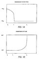
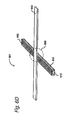
- Fig. 1A illustrates a resistance characteristic of an exemplary anti-fuse.
- the anti-fuse has an initial high resistance R1 AF .
- V C critical voltage
- current begins to flow through the anti-fuse.
- R2 AF relatively low resistance
- the anti-fuse breaks down to a relatively low resistance R2 AF . If the voltage Vc continues to be applied, a large current flows through the anti-fuse after time t 1 .
- An anti-fuse can be formed from insulator materials, a multi-layer stack of insulator materials separated by conducting materials, a matrix of insulating material containing dispersed conductive inclusions, amorphous and crystalline semiconductor materials, phase change materials, combinations of a multi-layer stack of Si and silicide-forming metals, etc. Generally, the anti-fuse is sandwiched between two conducting materials to enable applications of voltage across the anti-fuse.
- Insulator materials include SiO x , SiN x , SiO x N y , Alo x , TaO x , TiO x , AlN x and the like; amorphous and crystalline semiconductor materials include Si, Ge, alloys of Si and Ge, InTe, SbTe, GaAs, InSe, InSb, and the like; phase change materials include alloys containing at least two elements selected from Si, Ge, As, Se, In, Sn, Sb, Te, Pb, Bi, and the like; silicide-forming metals include W, Pt, Pd, Co, Ni, Ti, and the like and alloys thereof.
- the thickness of the anti-fuse is preferably between 0.5 nano-meter (nm) and 50 nm. However, the thickness may be set to an arbitrary range depending on the circumstances. For instance, if appreciable current flow is desired through the anti-fuse in a pre-breakdown condition, then the insulator thickness may be chosen to be less than about 5 nm so that significant quantum mechanical tunneling current can flow at a modest voltage. If amorphous and polycrystalline semiconductor materials are used, the thickness is preferably between 1 nm and 100 nm. Again, the thickness may be varied.
- the anti-fuse is an element that has an initial high resistance and changes to a relatively low resistance when a critical voltage is applied.
- the mechanism that achieves the different resistive states is different for different materials.
- anti-fuses formed from phase change materials have a high resistance when in an amorphous state and a low resistance when in a crystalline state.
- anti-fuses formed from multi-layer Si and silicide-forming metals have a high resistance when the multi-layer has not been converted to silicide and a low resistance when the multi-layer has been converted to the silicide. In both cases, many orders of magnitude separate the high and low resistance states.
- the fuse is an element that has an initial low resistance and changes to a high resistance, mostly to an open circuit when a critical current is applied.
- the fuse may be a thin film resistor, and may be formed from materials such as semiconductors (e.g. Si, Ge), conductors (e.g. Al, Cu, Ag, Au, Pt), low melting material (e.g. In , Zn, Sn, Pb), refractory metals (e.g. Ta, W), transition metals (Ni, Cr) and the like and any alloys thereof. It is even more beneficial if the fuse is vertically oriented, i.e. the direction of the current flow is substantially vertical within the fuse, since very small memory elements can be achieved with vertically oriented fuses.
- Fig. 1B illustrates a resistance characteristic of an exemplary fuse.
- the fuse has an initial low resistance R1 F .
- the fuse maintains the low resistance until a critical current I c is initiated at time t 1 .
- I 2 Rt heating causes the temperature of the fuse to increase, leading to thermal runaway; i.e. the continued dissipation of power through the fuse leads to additional heating, which leads to further increase in temperature, and so on.
- the I 2 Rt heating causes the fuse to melt and become an open circuit R2 F at time t 2 .
- the first, or initial, state is resistance R1 F , which can be controlled to a specified value through the choice of fuse materials and geometry.
- the second, or final state is R2 F , an open-circuit.
- a memory made of the first type (fuse/anti-fuse in series) of unit memory cells may be programmed by either applying a critical current, I C , to those cells in which the second state is desired and leaving those cells alone in which the first state is desired. Applying a read voltage V R and sensing a presence or absence of electrical current through the selected memory cell may detect the first and second states of an individual unit memory cell. Presence of current indicates that the memory cell is in the first state and absence of current indicates that the memory cell is in the second state.
- Figs. 1C illustrates a resistance (shown in solid line) and current (shown in dashed line) characteristics of an exemplary fuse/anti-fuse series combination.
- the high resistance R1 AF of the anti-fuse is dominant.
- V c voltage
- the anti-fuse breaks down at time t 1 as explained previously.
- both the fuse and the anti-fuse are low in resistance as shown by the sharp drop in the resistance line around time t 1 .
- Due to the low resistance current passing through the fuse/anti-fuse combination becomes critical, i.e. critical current I C is generated. This melts the fuse as discussed previously.
- the thermal runaway process causes the temperature to increase until finally the fuse breaks and becomes an open circuit at time t 2 .
- the fuse and anti-fuse combined resistance is the open circuit R2 F resistance.
- the current becomes zero at time t 2 as shown by the dashed lines in Fig. 1C.
- the memory cell with the fuse and anti-fuse in series exhibits two states.
- the first state or the initial state, exhibits a finite resistance (generally dominated by R1 AF ). In this first state, some amount of current may flow since the resistance is finite.
- the second state exhibits an infinite resistance (an open circuit R2 F ). As a result, no current may flow across the cell (see the dashed line in Fig. 1C).
- the anti-fuse provides selectivity for programming a particular memory cell. Also the high initial resistance of the anti-fuse allows the individual resistance of the fuse to be reduced to an arbitrary value without jeopardizing the ability to sense an individual memory element in the array.
- resistance of the anti-fuse may vary with different levels of the applied voltage. This characteristic can be used to enhance the memory cell selectivity function that an anti-fuse provides in memory devices. As seen in Fig. 1D, the resistance of a thin insulator type anti-fuse (metal/insulator/metal tunnel junction) is shown to generally decrease as the voltage across the anti-fuse increases. Thus by controlling the voltage across the anti-fuse, the effective resistance of the unit memory cell can be controlled as well. Note that the resistance-voltage characteristic may be non-linear.
- a second type of unit memory cell generally includes a vertically oriented fuse.
- Vertically oriented fuses have current flow that is vertical, i.e. perpendicular to the plane of the substrate.
- the vertically oriented fuses are manufactured such that a ratio of vertical height to lateral thickness of the fuse is at least 1, and is generally substantially greater than 1, perhaps as much as 30 to 1 or more, which again allows for high density memories to be fabricated.
- Programming and reading a memory made of unit memory cells of the second type is also relatively straightforward. Like the memories made of first type of unit memory cells, programming a second type of memory cell is achieved by applying a critical voltage V c (not necessarily the same critical voltage related to the first type) to generate a critical current I c (again, not necessarily the same as the first type) to melt the fuse. Also, first and second states are determined by applying a reading voltage and detecting presence or absence of current.
- equipotential methods may be used to read data from memory devices made of either the first or the second type of unit memory cells.
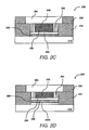
- Fig. 2A illustrates a cross-sectional view of a first embodiment of a unit memory cell 200 used as a basis to form an OTP memory according to an aspect of the invention.
- the unit memory cell 200 which is a first type of unit memory cell described above, includes a fuse 230 in series with an anti-fuse 280.
- the fuse and anti-fuse 230 and 280 are formed in a closed region 285.
- the fuse 230 is vertically oriented in relation to the substrate plane (not shown). In this manner, the current flow in the unit memory cell is also perpendicular (vertical) to the substrate plane. This allows memory cells to be inserted between adjacent conductor layers. In particular, the cells may be placed at an intersection of a cross-point array of conductors to form the cross-point memory array. Planes of these arrays can be stacked on top of one another, which increases the density of the OTP memory dramatically.
- the unit memory cell 200 may also include a column conductor 210; a first insulator 220 situated above the column conductor 210 and defining the closed region 285; an insulating plug 240 occupying a center region of the closed region 285 from a top of the anti-fuse 280; a second insulator 250 and a row conductor 260, both situated above the first insulator 220, the fuse 230 and the insulating plug 240.
- the anti-fuse 280 may be formed from insulator materials, a multi-layer stack of insulator materials separated by conducting materials, a matrix of insulating material containing dispersed conductive inclusions, amorphous and crystalline semiconductor materials, phase change materials, combinations of a multi-layer stack of Si and silicide-forming metals, etc.
- materials such as semiconductors, conductors, low melting temperature materials, refractory metals, transition metals and the like may be used.
- conductive materials such as Al, Cu, Ag, Au, W, and the like and any alloys thereof can be used.
- poly-silicon may be used for the row and column conductors 260 and 210.
- materials such as silicon oxides and nitrides, aluminum oxides and nitrides, silicon oxy-nitrides, tantalum oxides and the like may be used.
- etch away the insulating plug 240 may be desirable to etch away the insulating plug 240, wholly or partially, to leave a void.
- This configuration provides extremely low thermal conductivity adjacent to the fuse 230, and provides space for molten or evaporated fuse material to enter. These features lower the power necessary to break the fuse 230.
- the insulating plug 240 does help to control the cross-sectional area of the fuse 230 in a plane parallel to the substrate plane, for example the area of the fuse 230 contacting the anti-fuse 280. Controlling the cross-sectional area allows the characteristics of the fuse, and thus the memory cell to be manipulated precisely.
- Fig. 2A shows that the row conductor 260 covers the entirety of the fuse 230 at the top of the closed region 285. Similarly, Fig. 2A also shows that the column conductor 210 covers the entirety of the anti-fuse 280 at the bottom of the closed regi on 285. While complete coverage is shown, it is required only that a conductive path between the row and the column conductors 260 and 210 exists. Thus, electrical connections should exist among the column conductor 210, the fuse 230, the anti-fuse 280, and the row conductor 260. It is not necessary that the column conductor 210, the fuse 230, the anti-fuse 280, and the row conductor 260 be in physical contact with each other.
- Fig. 2B illustrates a top view of the unit memory cell 200 of Fig. 2A showing the fuse 230 and the insulating plug 240 substantially occupying the edge and center of the closed region 285, which is located within the cross-point 115 of the row and column conductors 260 and 210.
- the anti-fuse 280 (not shown in Fig. 2B) may have the same shape as the insulating plug 240 and fuse 230, or it can extend beyond the fuse 230 and assume a different shape.
- the row and column conductors 260 and 210 extend in their respective directions to form the cross-point 215 (shown as a dashed line region for illustrative purposes).
- the closed region 285 is shown to be entirely located within the cross-point 215, As noted above, it is only necessary that electrical connectivity be maintained between the row and column conductors 260 and 210 through the structure within the closed region 285.
- first and second insulators 220 and 250 are not included in Fig. 2B.
- the fuse 230 and the insulating plug 240 are shown at the cross point 215.
- the row conductor 260 covers the entirety of the fuse 230 and the insulating plug 240.
- the closed region 285 is shown as being cylindrical with the fuse 230 substantially occupying an annulus of the closed region 285 and the insulating plug 240 substantially occupying a center of the closed region 285.
- the shape of the closed region 285 is not so limited and may include other shapes as well, such as a rectangle, a square, an ellipse, or any other enclosed shape.
- the insulating plug 240 may be partially or wholly etched away to leave a void.
- Figs. 2C - 2D illustrate variations on the first embodiment of Fig. 2A.
- a thin conductor 290 may be placed as shown to enhance the performance of the memory cell 200.
- two thin conductors 290 and 290b may be placed as shown for the same purpose.
- the thin conductors 290 and/or 290b enable independent control of the material adjacent to the antifuse 280 and provide a larger contact area between the fuse 230 and the anti-fuse 280.
- the thin conductors 290 and/or 290b may be a Schottky or ohmic contact to the anti-fuse 280, or the thin conductors 290 and/or 290b may be a thermal insulator to better thermally isolate the fuse 230.
- the thin conductors 290 and/or 290b may be formed of Al, Cu, Ni, Ti, W, W, metal nitrides, doped silicon, Ta, and the like and the alloys thereof.
- the thin conductor 290 is placed between the anti-fuse 280 and the fuse 230 in the closed region 285. If only a single thin conductor is to be included, this is the preferred placement in order to increase the area of the top surface of the anti-fuse 280.
- the first thin conductor 290 is placed between the anti-fuse 280 and the fuse 230 as in Fig. 2C, but also includes a second thin conductor 290b placed between the column conductor 210 and the anti-fuse 280.
- thin conductors 290 and/or 290b are to introduce a material with lower thermal conductivity than present in the row or column conductors 260 or 210.
- a layer with low thermal conductivity may help to thermally isolate the memory cell from the row or column conductors 260 or 210. Thermal isolation provides for more efficient use of heat generated by I 2 Rt processes.
- amorphous or crystalline semiconductors as the anti-fuse introduces additional reasons to include the thin conductors 290 and/or 290b.
- the choice of conductor material in contact with the semiconductor determines whether a rectifying or ohmic contact is formed. The nature of this contact may affect the function of the anti-fuse 280.
- the low resistance state is created by metal migration through the semiconductor layer. This process generally depends on the type of metal adjacent to the semiconductor. This provides flexibility in the choice of the conductors 210 and 260 and the metal layer adjacent to the semiconductor or anti-fuse, in this case, the thin conductors 290 and/or 290b.
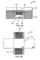
- Fig. 3A illustrates a cross-sectional view of a first example of a unit memory cell 300 used as a basis to form an OTP memory useful in explaining the invention.
- the unit memory cell 300 which is also a first type of unit memory cell, may include a fuse 330 and an insulator 320 formed on either side of the fuse 330.
- the interior of the fuse 330 may or may not be completely filled.
- the cell 300 may also include a bottom conductor 310. Note that vertical portions of the fuse 330 and the bottom conductor 310 make up a 'U' region 385. In other words, the horizontal portion of the fuse 330 of Fig. 3A is not necessary.
- the cell 300 may further include an insulating plug 340 occupying some or substantially most of the interior of the 'U' region 385.
- the cell 300 further includes an anti-fuse 380 and a top conductor 360 above the above the 'U' region 385 and the insulator 320.
- Fig. 3B illustrates a top view of the unit memory cell 300 of Fig. 3A.
- the row conductor 360 may extend in a row direction.
- the anti-fuse 380 (not visible in Fig. 3B) may also extend in the row direction.
- the anti-fuse 380 may also extend in a column direction on top of the fuse 330 and insulating plug 340.
- the anti-fuse material 380' is an insulator, the anti-fuse 380 does not require patterning since it is by definition insulating in the plane of the film.
- the fuse 330, and thus the 'U' region 385, including the insulating plug 340 and the bottom conductor 310 may extend in the column direction and thereby defining a cross-point at the intersection.
- Figs. 3C - 3F illustrate variations on the unit memory cell 300 of Fig. 3A.
- a thin conductor 390 may be placed between the fuse 330 and the anti-fuse 380 to enhance performance of the memory cell 300 as discussed previously with respect to the variations on the first embodiment. Note that the placement of the thin conductor 390 may be varied and is not limited to the placement as shown in Fig. 3C. However, the thin conductor 390 may be substantially limited to an area defined by a cross-point 315 as shown in Fig. 3B.
- Figs. 3D in addition to clarifying the 'U' region 385, also illustrates a variation on the unit memory cell 300 of Fig. 3A. As noted above, the horizontal portion of the fuse 330 is not necessary. Fig. 3D demonstrates this concept.
- Fig. 3E demonstrates that the thin conductor 390 need not cover the entirety of the 'U' region 385.
- the thin conductor 330 is formed substantially within the interior of the 'U' region 385 and the fuse 330 is in contact with the anti-fuse 380. Note that many other variations are possible.
- the fuse 330, insulating plug 340, and 'U' region 385 extend in a second direction along with the bottom conductor 310
- this orientation is not required.
- the fuse 330 can be associated with the top conductor 360 and extend in a first direction.
- the vertical portions of the fuse 330 and the top conductor 360 now make up an inverted 'U' region 385.
- An insulating plug 340 can once again occupy some or substantially all of the inverted 'U' region 385.
- the memory cell 300 further includes an anti-fuse 380 and a substantially occupying the bottom of the inverted 'U' region 385 above bottom conductor 310.
- An example of this alternate configuration is illustrated in Fig. 3F.
- Fig. 4A illustrates a cross-sectional view of a second example of a unit memory cell 400 used as a basis to form an OTP memory useful in explaining the invention.
- the unit memory cell 400 which is a second type of unit memory cell, includes a vertically oriented fuse 430.
- the vertically oriented fuse 430 is formed in a closed region 485.
- the unit memory cell 400 may also include a column conductor 410; a first insulator 420 situated above the column conductor 410 and defining the closed region 485; an insulating plug 440 occupying a center region of the closed region 485; a second insulator 450 and a row conductor 460, both situated above the first insulator 420 and the vertically oriented fuse 430.
- the materials used to form the various parts of the memory cell have been discussed above. Also as discussed above, the insulating plug 440 is not strictly necessary. Like the first embodiment, complete coverage of the vertically oriented fuse 430 by the row conductor 460 is shown.
- Fig. 4B illustrates a top view of the unit memory cell 400 of Fig. 4A showing the fuse 430 and the insulating plug 440 substantially occupying the edge and center of the closed region 485, which is located within the cross-point 415 of the row and column conductors 460 and 410.
- Fig. 5A illustrates a cross-sectional view of a third example of a unit memory cell 500 used as a basis to form an OTP memory useful in explaining the invention.
- the unit memory cell 500 which is again a second type of unit memory cell, may include a vertically oriented fuse 530 and an insulator 520 formed on either side of the vertically oriented fuse 530.
- the interior of the vertically oriented fuse 530 may or may not be completely filled.
- the cell 500 may also include a bottom conductor 510. Note that vertical portions of the vertically oriented fuse 530 and the bottom conductor 510 make up a 'U' region 585. In other words, the horizontal portion of the fuse 530 of Fig. 3A is not necessary This is shown in Fig. 5C.
- the cell 500 may further include an insulating plug 540 occupying some or most of the interior of the 'U' region 585.
- the cell 500 may still further include a top conductor 560 above the above the 'U' region 585 and the insulator 520.
- Fig. 5B illustrates a top view of the unit memory cell 500 of Fig. 5A.
- the row conductor 560 may extend in a row direction.
- the vertically oriented fuse 530, and thus the 'U' region 585, including the insulating plug 540 and the bottom conductor 510 (both not shown in Fig. 5B) may extend in the column direction and thereby defining a cross-point 515 at the intersection.
- the fuse 530 may be associated with the top conductor 360 and extend in a first direction.
- Fig. 6A illustrates a simplified three-dimensional perspective of a unit memory cell 600 of a memory array according to an aspect of the invention.
- the memory cell 600 includes a row and column conductors 660 and 610.
- the row and column conductors 660 and 610 may correspond to the top and bottom conductors of unit memory cell embodiments shown in Figs. 2A-5C.
- a state element 692 is formed in between the conductors.
- the state element 692 corresponds to the first type of unit memory cells as shown in Figs. 2A-3E-For simplicity, insulators that may normally surround the state element 692 are not included in Fig. 6A.
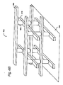
- Figs. 6B-6C illustrate simplified three-dimensional perspectives of stacked memory arrays according to an aspect of the invention.
- a memory 602 includes a plurality of row conductors 660, a plurality of column conductors 610, and a plurality of state elements 692. Where the row and column conductors 660 and 610 define a cross-point, a state element 692 maybe placed. The entire memory 602 may be placed above a substrate 699.
- a memory array may be defined as a plurality of state elements 692 that are all on a same level.
- the row and column conductors 660 and 610 may also be a part of the memory array.
- Fig. 6B there are three memory arrays stacked on top of one another. However, many levels of memory array may be stacked. Again, insulators that may normally surround the state elements 692 are not included in Fig. 6B for simplicity.
- the memory arrays shown in Fig. 6B are stacked such that three memory arrays require four conductor levels. This can be generalized to a memory with N memory arrays requiring N+1 conductor levels. It is also possible to configure the memory arrays such that N memory arrays require 2N conductor levels; for example, in Fig. 6C where two memory arrays and four conductor levels are shown. In this configuration, each memory plane is electrically independent of other memory planes.
- Fig. 6B shows cylindrical state elements 692
- Fig. 6C shows a memory 604 with rectangular state elements 694. This is to illustrate that the shape of the state element is not limited to any particular shape.
- Fig. 6D illustrates a three-dimensional perspective of the unit memory cell 300 of Figs. 3A-3E, relabeled as 601 in this figure.
- the memory cell 601 includes row and column conductors 662 and 612, a fuse 632, and an insulating plug 642.
- the combination of the fuse 632 and the anti-fuse 682 may comprise a state element 696 at the cross-point of the row and column conductors 662 and 612. If the anti-fuse 682 were removed, Fig. 3d would illustrate a three-dimensional perspective of the unit memory cell 500 of Figs. 5A-5C. Again for simplicity, insulators that may normally surround the state element 696 are not included in Fig. 6D.
- Fig. 6E illustrates a simplified three-dimensional perspective of stacked memory arrays according to the invention.
- a memory 606 may include a plurality of row conductors 662, a plurality of column conductors 612, a plurality of fuses 632, and a plurality of insulating plugs 642. Again, the memory 606 includes an anti-fuse 682 at each memory cell 696. The entire memory 606 may be placed above a substrate 699.
- three levels of memory array are shown, but in reality, many levels of memory array may exist.
- N layers of memory and 2N layers of conductors are shown.
- An alternative configuration has N memory layers for N+1 conductor layers.
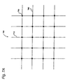
- Fig. 7A illustrates a two-dimensional representation of a memory array 700 according to an aspect of the invention.
- the memory array may include one or more row conductors 760 and one or more column conductors 710. At intersections (cross-points) between the row and column conductors 760 and 710, state elements 790 are formed.
- the state elements 790 may be a first or second type of unit memory cells.
- the particular state element 790 may be electrically connected to a particular row conductor 760 and also to a particular column conductor 710. Selecting a particular state element 790 then becomes a simple exercise of activating the particular row and column conductors.
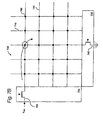
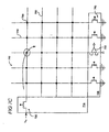
- Figs. 7B and 7C illustrate a representation of a memory array 700 for programming and reading, respectively, according to aspects of the invention.
- the memory array 700 may further include a row addressing circuit 715 and a column addressing circuit 735.
- the row addressing circuit 715 may include multiple row transistors 725 where each row conductor 760 is connected to at least one row transistor 725.
- the column addressing circuit 735 may include multiple column transistors 745 where each column conductor 710 is connected to at least one column transistor 745. Further, as shown in Fig. 7C, the column addressing circuit 745 may also include multiple current sensors 755 where each column conductor 710 is connected to at least one current sensor 755.
- Fig. 7D illustrates a current sensor 755 that utilizes equipotential sensing.
- the magnitude of a sense current from the current sensor 755 indicates the resistance of the state element 790, i.e. the unit memory cell of first or second type, which is then used to determine the logic state of the state element 790.
- a ground potential (or some other common equalized potential) is typically applied to non-selected column conductors 710.
- the ground potential may be applied using transistors 745 for example.
- a virtual ground potential is applied to the input of the current sensor 755.
- the selected column conductor 710 could be connected to the input of the current sensor 755.
- the potentials of the selected and non-selected column conductors 710 are substantially equalized. This equalization keeps substantially all of the sense current Is flowing to the current sensor 755.
- the equalization substantially blocks the currents from non-selected column conductors from straying into the selected column conductor 710. The blocking minimizes interference with the sensing current Is, which in turn preserves or increases the signal-to-noise ratio during the read operation.
- the read voltage V R may be increased or decreased as necessary.
- the effect is more noticeable for memories using the fuse/anti-fuse combination unit memory cells. It was described above that the resistance of the anti-fuse generally decreases as the voltage across the anti-fuse increases (see Fig. 1D).
- increasing the voltage across the memory cell results in an increase in current not only due to increased voltage, but also due to the decreased resistance.
- a linear increase/decrease in the reading voltage can lead to more than a linear increase/decrease in current. This characteristic can be used to enhance the reading sensitivity of the memory 700.
- An additional feature of the voltage dependence of the anti-fuse resistance in a fuse/anti-fuse cross-point memory is that unselected memory cells may have substantially higher resistance than the selected memory cell. As a consequence, the leakage current into the selected column due to current flow through unselected memory cells may be substantially reduced.
- the cross-point memory array 700 does not require a silicon substrate. This allows many memory array layers to be fabricated on top of each other.
- the arrays may be connected to CMOS support circuits.
- the support circuitries include the row and column addressing circuitries 715 and 735, as well as the read and write circuitries (not shown).
- the support circuits may be fabricated under the cross-point memory array 700. In this manner, the silicon substrate real estate may be more efficiently used and higher memory capacity may be achieved.
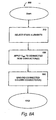
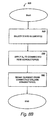
- Figs. 8A and 8B illustrate flow diagrams of methods of programming (800) and reading (805) a memory, respectively, according to an aspect of the invention.
- Fig. 8A when programming the memory device made of memory arrays such as shown in Fig. 7B, one or more state elements 790 are selected (step 810).
- the programming of a state element 790 may be performed by applying a writing voltage V WR to the connected row conductor 760 (step 820) and grounding the connected column conductor 710 (step 830).
- the steps 820 and 830 may be performed in opposite order or simultaneously.
- FIG. 7B An example of the programming method 800 is next described with reference to Fig. 7B.
- the state element 790 at the intersection of the top row and the third column is selected and the voltage drop occurs across the selected 790.
- the voltage V WR should to be sufficiently large to cause the critical voltage drop to occur across the selected state element 790.
- the arrow indicates the direction of flow of the sense current I s , which in this case is from the top row conductor 760 to the third column conductor 710.
- multiple state elements 790 may be selected and programmed by appropriately selecting the row and column conductors and supplying sufficient voltage and current. For example, assume that V WR is applied to first row conductor 760 (as in Fig. 7B). However, in addition to the third column conductor 710, assume also that the fourth column conductor 710 is grounded. Then both the third and fourth state elements 790 of the first row may be programmed simultaneously.
- one or more state elements 790 are selected (step 840). For each selected state element 790, the reading may be accomplished by applying a reading voltage V R to the row conductor 760 (step 850) and sensing the amount of current from the column conductor 710 connected to the selected state element 790 (step 860).
- Fig. 7C An example of the reading method 805 is next described with reference to Fig. 7C.
- Fig. 7C the state element 790 at the intersection of the top row and the third column is selected and the voltage drop occurs across the selected state element 790.
- the arrow indicates the direction of the current flow, which in this case is from the top row conductor to the third column conductor.
- Low resistance and high resistance are two possible states for a state element.
- the low resistance indicates that the state element 790 has remained in the initial state and the high resistance indicates that the state element 790 has changed to a programmed state.
- the initial state may be detected by presence of a current due to a finite resistance (fuse not blown) and the programmed state may be detected by the absence of current due to an open circuit (fuse blown).
- multiple state elements 790 may be selected and read by appropriately selecting the row and column conductors and sensing the current flow.
Description
- The present invention relates generally to programmable memory storage devices. More particularly, the invention relates to a one-time programmable storage device with fuse and anti-fuse combination unit memory cells.
- The demand for semiconductor devices has increased dramatically in recent years as evidenced by the pervasiveness of consumer electronic devices. Most or all consumer electronics are possible because of developments in semiconductor devices. As the electronic devices become smaller, more sophisticated, and less expensive, the demand for highly dense semiconductor devices at a lower cost is increasing.
- In the field of memories, the demand for ever increasing densities and lower cost is particularly true, especially for non-volatile memories, i.e., those memories that do not lose data even when power is not supplied.
- A non-volatile memory may be a one-time programmable ("OTP") or re-programmable. As the name suggests, OTP memory is programmed once, and it is permanent for all practical purposes. Most OTP memories can be categorized into four basic types: 1) anti-fuse, 2) fuse, 3) charge storage (EPROM), and 4) mask ROM.
- Programmable elements based on an anti-fuse typically rely on breakdown of metal-insulator-metal or diode structures to create the two resistance states. Programming voltages in excess of 10 V are generally required. In addition, the current required for anti-fuse breakdown can be large, which leads to large drive transistors. If used as a memory cell, an access transistor is typically included in the memory cell.
- Memory cells based on a fuse storage element are not widely used due to the large cell size. A planar fuse requires a minimum area of 8λ2 (where λ is the minimum photolithographic feature size), since a contact region is needed on each end of the fuse. Generally the fuse is even larger than 8λ2 to provide a more readily programmed element. As for the anti-fuse, the programming current can be large, which leads to large drive transistors as mentioned above. Adding an access transistor increases the minimum cell size even further.
- In the case of EPROM, programming the bit requires a high write voltage to transfer charge from the substrate to the floating gate of the memory cell by Fowler-Nordheim electron tunneling. Write speed is limited by the tunneling current density. EPROM is unique within the OTP memory family in that it can be reprogrammed, but it has to be erased first by exposing the memory array to a ultra-violet light source. This procedure is not easily implemented and the entire memory is erased.
- A mask read only memory ("mask ROM") is a memory that is programmed at the time of fabrication, and thus is a type of an OTP memory. A mask ROM is relatively simpler since the circuit to enable writing is not needed, and thus is less costly when compared to other OTP memories. Because the programming is part of the fabrication process, the mask ROM cannot be "field programmed", i.e., programmed by the purchaser to fit the particular needs of the purchaser. In other words, mask ROMs do not provide the flexibility of field programmability. Also, unless the mask ROMs are manufactured in bulk, cost savings cannot generally be realized.
- Existing OTP memory technologies described above are based on cell sizes considerably larger than 4λ2, the minimum cell size for a cross-point memory. In addition, in each case the memory cell consists of a single plane of memory elements constructed on a single crystal silicon substrate, with the sense and programming electronics located around the periphery of the memory array. Consequently, high density, low cost OTP memories are difficult to fabricate.
-
US-A-3,717,857 discloses a rewritable read-only memory in which diode elements are located between word lines and bit lines at cross-points of the lines. -
US-A-6,1 85, 122 andUS-A-5,451,811 (discloses a one-time programmable memory that include a memory array which comprises: one or more row conductors extending in a row direction, one or more column conductors extending in a column direction such that a cross-point is formed at intersections between said row and column conductors, and a state element including a fuse and an anti-fuse in series with each other, the state element being in electrical contact with said row and column conductors. - According to the present invention, there is provided a one-time programmable memory comprising a memory array, which comprises:
- one or more row conductors extending in a row direction;
- one or more column conductors extending in a column direction such that a cross-point in formed at intersections between said row and column conductors; and
- a state element including a fuse having a fuse axis extending generally vertically between the row conductor(s) and the column conductor(s) and an anti-fuse having an antifuse-axis extending generally vertically between the row conductor(s) and the column conductor(s), the fuse and the antifuse being in series with each other, said state element being in electrical contact with said row and column conductors,
- A method of programming an OTP memory may include the steps of selecting a state element, applying a writing voltage VWR to a row conductor electrically connected to the selected state element, and grounding a column conductor electrically connected to the selected state element. By applying voltage VWR to the row conductor and grounding the column conductor, a critical voltage drop Vc occurs through the selected state element causing the state element to change states.
- A method of reading an OTP memory may include the steps of selecting a state element, applying a reading voltage VRD to a row conductor electrically connected to the selected state element, and sensing an amount of current from a column conductor electrically connected to the selected state element. Sensing a relatively high current indicates that the state element is in a first state (a low resistance state) and sensing a relatively low current indicates that the state element is in a second state (a high resistance state).
- Certain advantages follow from certain embodiments of the invention. For example, the size of individual unit memory cell is dramatically reduced. This enables providing a high density OTP memory cell at much lower cost. Also, the unit memory cells may be fabricated using standard semiconductor processes and materials, and thus, little to no capital investment is required beyond that present in the current state-of-the-art manufacturing. Further, the current flow in the memory cells is substantially perpendicular (vertical) to the substrate plane. This allows the cells to be inserted between adjacent conductors. In particular, the cells can be placed at an intersection of a cross-point array of conductors to form a cross-point OTP memory array. The cross-point memory arrays can be fabricated such that the planar area of each memory cell is 4λ2. Planes of these arrays can be stacked on top of one another, which increases the density dramatically.
- Features and advantages of the invention will become apparent to those skilled in the art from the following description with reference to the drawings, in which:
- Fig. 1A illustrates a resistance characteristic of an exemplary anti-fuse according to an aspect of the invention;
- Fig. 1B illustrates a resistance characteristic of an exemplary fuse according to an aspect of the invention;
- Fig. 1C illustrates the resistance and current characteristic of an exemplary fuse/anti-fuse series combination used in a unit memory cell according to an aspect of the invention;
- Fig. 1D illustrates the voltage-resistance characteristic of the anti-fuse;
- Figs. 2A illustrates a cross-sectional view of a first embodiment of a unit memory cell used as a basis to form an OTP memory according to an aspect of the invention;
- Fig. 2B illustrates a top view the unit memory cell of Fig. 2A showing the cross-point nature of the unit memory cell;
- Figs. 2C - 2D illustrate variations on the unit memory cell of Fig. 2A according to aspects of the invention;
- Fig. 3A illustrates a cross-sectional view of a first example of a unit memory cell used as a basis to form an OTP memory useful in explaining the invention;
- Fig. 3B illustrates a top view the unit memory cell of Fig. 3A showing the cross-point nature of the unit memory cell;
- Figs. 3C - 3F illustrate variations on the unit memory cell of Fig. 3A;
- Fig. 4A illustrates a cross-sectional view of a second example of a unit memory cell used as a basis to form an OTP memory useful in explaining the invention;
- Fig. 4B illustrates a top view the unit memory cell of Fig. 4A showing the cross-point nature of the unit memory cell;
- Fig. 5A illustrates a cross-sectional view of a third example of a unit memory cell used as a basis to form an OTP memory useful in explaining the invention;
- Fig. 5B illustrates a top view the unit memory cell of Fig. 5A showing the cross-point nature of the unit memory cell;
- Figs. 5C illustrates a variation on the unit memory cell of Fig. 5A;
- Fig. 6A illustrates a simplified three-dimensional perspective of a unit memory cell of a memory array according to an aspect of the invention;
- Figs. 6B-6C illustrate simplified three-dimensional perspectives of stacked memory arrays using the unit memory cells according to an aspect of the invention;
- Fig. 6D illustrates a simplified three-dimensional perspective of another unit memory cell of a memory array useful in explaining the invention;
- Fig. 6E illustrates a simplified three-dimensional perspectives of stacked memory arrays using the unit memory cell of Fig. 4D useful in explaining the invention;
- Fig. 7A illustrates a two-dimensional representation of a memory array according to an aspect of the invention;
- Figs. 7B and 7C illustrate representations of a memory array for programming and reading, respectively, according to aspects of the invention;
- Fig. 7D illustrates a current sensor that utilizes an exemplary equalized potential sensing method to read memory cells according to an aspect of the invention; and
- Figs. 8A and 8B illustrate flow diagrams of methods of programming and reading a memory, respectively, according to an aspect of the invention.
- For simplicity and illustrative purposes, the principles of the invention are described by referring mainly to exemplary embodiments thereof. However, one of ordinary skill in the art would readily recognize that the same principles are equally applicable to many types of one-time programmable (OTP) memories and methods of using thereof.
- In general, an OTP memory is formed using one or more cross-point memory arrays, and the memory arrays are formed using unit memory cells. A unit memory cell, according to certain aspects of the invention, is located at a cross-point of two conductors. A first type of unit memory cell generally includes a fuse in series with an anti-fuse. The anti-fuse is an element that has an initial high resistance and breaks downs to a relatively low resistance when a critical voltage is applied.
- Fig. 1A illustrates a resistance characteristic of an exemplary anti-fuse. As shown, the anti-fuse has an initial high resistance R1AF. When a critical voltage VC is applied at time to, current begins to flow through the anti-fuse. At time t1, the anti-fuse breaks down to a relatively low resistance R2AF. If the voltage Vc continues to be applied, a large current flows through the anti-fuse after time t1.
- An anti-fuse can be formed from insulator materials, a multi-layer stack of insulator materials separated by conducting materials, a matrix of insulating material containing dispersed conductive inclusions, amorphous and crystalline semiconductor materials, phase change materials, combinations of a multi-layer stack of Si and silicide-forming metals, etc. Generally, the anti-fuse is sandwiched between two conducting materials to enable applications of voltage across the anti-fuse. Insulator materials include SiOx, SiNx, SiOxNy, Alox, TaOx, TiOx, AlNx and the like; amorphous and crystalline semiconductor materials include Si, Ge, alloys of Si and Ge, InTe, SbTe, GaAs, InSe, InSb, and the like; phase change materials include alloys containing at least two elements selected from Si, Ge, As, Se, In, Sn, Sb, Te, Pb, Bi, and the like; silicide-forming metals include W, Pt, Pd, Co, Ni, Ti, and the like and alloys thereof.
- If insulator materials are used as the anti-fuse, then the thickness of the anti-fuse is preferably between 0.5 nano-meter (nm) and 50 nm. However, the thickness may be set to an arbitrary range depending on the circumstances. For instance, if appreciable current flow is desired through the anti-fuse in a pre-breakdown condition, then the insulator thickness may be chosen to be less than about 5 nm so that significant quantum mechanical tunneling current can flow at a modest voltage. If amorphous and polycrystalline semiconductor materials are used, the thickness is preferably between 1 nm and 100 nm. Again, the thickness may be varied.
- As noted above, the anti-fuse is an element that has an initial high resistance and changes to a relatively low resistance when a critical voltage is applied. The mechanism that achieves the different resistive states is different for different materials. For example, anti-fuses formed from phase change materials have a high resistance when in an amorphous state and a low resistance when in a crystalline state. Also, anti-fuses formed from multi-layer Si and silicide-forming metals have a high resistance when the multi-layer has not been converted to silicide and a low resistance when the multi-layer has been converted to the silicide. In both cases, many orders of magnitude separate the high and low resistance states.
- As another example, if an insulator type of anti-fuse is used, up to the critical voltage V c , current passes through the insulating barrier of the metal-insulator-metal structure by electron tunneling, and the specific resistance of the cell can be rather large, for example, on the order of 107 Ω-µm2. However, beyond the critical voltage Vc, the barrier breaks down due to metal migration through the insulator, and the specific resistance of the cell can drop to below 100 Ω-µm2. Similar current transport and breakdown mechanisms are operative in layered insulators and insulators containing conductive inclusions.
- Unlike the anti-fuse, the fuse is an element that has an initial low resistance and changes to a high resistance, mostly to an open circuit when a critical current is applied. The fuse may be a thin film resistor, and may be formed from materials such as semiconductors (e.g. Si, Ge), conductors (e.g. Al, Cu, Ag, Au, Pt), low melting material (e.g. In, Zn, Sn, Pb), refractory metals (e.g. Ta, W), transition metals (Ni, Cr) and the like and any alloys thereof. It is even more beneficial if the fuse is vertically oriented, i.e. the direction of the current flow is substantially vertical within the fuse, since very small memory elements can be achieved with vertically oriented fuses.
- Fig. 1B illustrates a resistance characteristic of an exemplary fuse. As shown, the fuse has an initial low resistance R1F. The fuse maintains the low resistance until a critical current Ic is initiated at time t1. At this point, I2Rt heating causes the temperature of the fuse to increase, leading to thermal runaway; i.e. the continued dissipation of power through the fuse leads to additional heating, which leads to further increase in temperature, and so on. Eventually the I2Rt heating causes the fuse to melt and become an open circuit R2F at time t2. Thus, the memory cell with a fuse exhibits two states. The first, or initial, state is resistance R1F, which can be controlled to a specified value through the choice of fuse materials and geometry. The second, or final state is R2F, an open-circuit.
- A memory made of the first type (fuse/anti-fuse in series) of unit memory cells may be programmed by either applying a critical current, IC, to those cells in which the second state is desired and leaving those cells alone in which the first state is desired. Applying a read voltage VR and sensing a presence or absence of electrical current through the selected memory cell may detect the first and second states of an individual unit memory cell. Presence of current indicates that the memory cell is in the first state and absence of current indicates that the memory cell is in the second state.
- Figs. 1C illustrates a resistance (shown in solid line) and current (shown in dashed line) characteristics of an exemplary fuse/anti-fuse series combination. Initially, the high resistance R1AF of the anti-fuse is dominant. However, when sufficiently large voltage, i.e. Vc, is applied at time to, the anti-fuse breaks down at time t1 as explained previously. At this point, both the fuse and the anti-fuse are low in resistance as shown by the sharp drop in the resistance line around time t1. Due to the low resistance, current passing through the fuse/anti-fuse combination becomes critical, i.e. critical current IC is generated. This melts the fuse as discussed previously. The thermal runaway process causes the temperature to increase until finally the fuse breaks and becomes an open circuit at time t2. At this point, the fuse and anti-fuse combined resistance is the open circuit R2F resistance. Correspondingly, the current becomes zero at time t2 as shown by the dashed lines in Fig. 1C.
- Thus the memory cell with the fuse and anti-fuse in series exhibits two states. The first state, or the initial state, exhibits a finite resistance (generally dominated by R1AF). In this first state, some amount of current may flow since the resistance is finite. The second state exhibits an infinite resistance (an open circuit R2F). As a result, no current may flow across the cell (see the dashed line in Fig. 1C).
- Programming and reading such a memory cell becomes a relatively simple task. If the first state is desired, the memory cell may be left alone. If the second state is desired, then a critical voltage Vc may be applied to the memory cell. Also the time between t1 to and t2 may be extremely short. This allows rapid programming to take place.
- in a cross-point memory array that does not include a diode or transistor in series with the memory cell, the anti-fuse provides selectivity for programming a particular memory cell. Also the high initial resistance of the anti-fuse allows the individual resistance of the fuse to be reduced to an arbitrary value without jeopardizing the ability to sense an individual memory element in the array.
- In addition, resistance of the anti-fuse may vary with different levels of the applied voltage. This characteristic can be used to enhance the memory cell selectivity function that an anti-fuse provides in memory devices. As seen in Fig. 1D, the resistance of a thin insulator type anti-fuse (metal/insulator/metal tunnel junction) is shown to generally decrease as the voltage across the anti-fuse increases. Thus by controlling the voltage across the anti-fuse, the effective resistance of the unit memory cell can be controlled as well. Note that the resistance-voltage characteristic may be non-linear.
- A second type of unit memory cell generally includes a vertically oriented fuse. Vertically oriented fuses have current flow that is vertical, i.e. perpendicular to the plane of the substrate. The vertically oriented fuses are manufactured such that a ratio of vertical height to lateral thickness of the fuse is at least 1, and is generally substantially greater than 1, perhaps as much as 30 to 1 or more, which again allows for high density memories to be fabricated.
- Programming and reading a memory made of unit memory cells of the second type is also relatively straightforward. Like the memories made of first type of unit memory cells, programming a second type of memory cell is achieved by applying a critical voltage Vc (not necessarily the same critical voltage related to the first type) to generate a critical current Ic (again, not necessarily the same as the first type) to melt the fuse. Also, first and second states are determined by applying a reading voltage and detecting presence or absence of current.
- As will be seen later, equipotential methods may be used to read data from memory devices made of either the first or the second type of unit memory cells.
- Fig. 2A illustrates a cross-sectional view of a first embodiment of a
unit memory cell 200 used as a basis to form an OTP memory according to an aspect of the invention. Theunit memory cell 200, which is a first type of unit memory cell described above, includes afuse 230 in series with an anti-fuse 280. The fuse and anti-fuse 230 and 280 are formed in aclosed region 285. - In this particular embodiment, the
fuse 230 is vertically oriented in relation to the substrate plane (not shown). In this manner, the current flow in the unit memory cell is also perpendicular (vertical) to the substrate plane. This allows memory cells to be inserted between adjacent conductor layers. In particular, the cells may be placed at an intersection of a cross-point array of conductors to form the cross-point memory array. Planes of these arrays can be stacked on top of one another, which increases the density of the OTP memory dramatically. - The
unit memory cell 200 may also include acolumn conductor 210; afirst insulator 220 situated above thecolumn conductor 210 and defining theclosed region 285; an insulatingplug 240 occupying a center region of theclosed region 285 from a top of the anti-fuse 280; asecond insulator 250 and arow conductor 260, both situated above thefirst insulator 220, thefuse 230 and the insulatingplug 240. - As noted above, the anti-fuse 280 may be formed from insulator materials, a multi-layer stack of insulator materials separated by conducting materials, a matrix of insulating material containing dispersed conductive inclusions, amorphous and crystalline semiconductor materials, phase change materials, combinations of a multi-layer stack of Si and silicide-forming metals, etc. To form the
fuse 230, materials such as semiconductors, conductors, low melting temperature materials, refractory metals, transition metals and the like may be used. - To form the row and
column conductors column conductors second insulators plug 240, materials such as silicon oxides and nitrides, aluminum oxides and nitrides, silicon oxy-nitrides, tantalum oxides and the like may be used. - Although not shown, in certain embodiments, it may be desirable to etch away the insulating
plug 240, wholly or partially, to leave a void. This configuration provides extremely low thermal conductivity adjacent to thefuse 230, and provides space for molten or evaporated fuse material to enter. These features lower the power necessary to break thefuse 230. - However, the insulating
plug 240 does help to control the cross-sectional area of thefuse 230 in a plane parallel to the substrate plane, for example the area of thefuse 230 contacting the anti-fuse 280. Controlling the cross-sectional area allows the characteristics of the fuse, and thus the memory cell to be manipulated precisely. - Fig. 2A shows that the
row conductor 260 covers the entirety of thefuse 230 at the top of theclosed region 285. Similarly, Fig. 2A also shows that thecolumn conductor 210 covers the entirety of the anti-fuse 280 at the bottom of the closed regi on 285. While complete coverage is shown, it is required only that a conductive path between the row and thecolumn conductors column conductor 210, thefuse 230, the anti-fuse 280, and therow conductor 260. It is not necessary that thecolumn conductor 210, thefuse 230, the anti-fuse 280, and therow conductor 260 be in physical contact with each other. - Fig. 2B illustrates a top view of the
unit memory cell 200 of Fig. 2A showing thefuse 230 and the insulatingplug 240 substantially occupying the edge and center of theclosed region 285, which is located within the cross-point 115 of the row andcolumn conductors plug 240 and fuse 230, or it can extend beyond thefuse 230 and assume a different shape. The row andcolumn conductors closed region 285 is shown to be entirely located within the cross-point 215, As noted above, it is only necessary that electrical connectivity be maintained between the row andcolumn conductors closed region 285. - For simplicity, the first and
second insulators fuse 230 and the insulatingplug 240 are shown at thecross point 215. However, therow conductor 260 covers the entirety of thefuse 230 and the insulatingplug 240. - Also, in Fig. 2B, the
closed region 285 is shown as being cylindrical with thefuse 230 substantially occupying an annulus of theclosed region 285 and the insulatingplug 240 substantially occupying a center of theclosed region 285. However, the shape of theclosed region 285 is not so limited and may include other shapes as well, such as a rectangle, a square, an ellipse, or any other enclosed shape. Again, the insulatingplug 240 may be partially or wholly etched away to leave a void. - Figs. 2C - 2D illustrate variations on the first embodiment of Fig. 2A. In Fig. 2C, a
thin conductor 290 may be placed as shown to enhance the performance of thememory cell 200. In Fig. 2D, twothin conductors thin conductors 290 and/or 290b enable independent control of the material adjacent to theantifuse 280 and provide a larger contact area between thefuse 230 and the anti-fuse 280. Thethin conductors 290 and/or 290b may be a Schottky or ohmic contact to the anti-fuse 280, or thethin conductors 290 and/or 290b may be a thermal insulator to better thermally isolate thefuse 230. Thethin conductors 290 and/or 290b may be formed of Al, Cu, Ni, Ti, W, W, metal nitrides, doped silicon, Ta, and the like and the alloys thereof. - In Fig. 2C, the
thin conductor 290 is placed between the anti-fuse 280 and thefuse 230 in theclosed region 285. If only a single thin conductor is to be included, this is the preferred placement in order to increase the area of the top surface of the anti-fuse 280. In Fig. 2D, the firstthin conductor 290 is placed between the anti-fuse 280 and thefuse 230 as in Fig. 2C, but also includes a secondthin conductor 290b placed between thecolumn conductor 210 and the anti-fuse 280. - One reason to include
thin conductors 290 and/or 290b is to introduce a material with lower thermal conductivity than present in the row orcolumn conductors column conductors - Using amorphous or crystalline semiconductors as the anti-fuse introduces additional reasons to include the
thin conductors 290 and/or 290b. First, the choice of conductor material in contact with the semiconductor determines whether a rectifying or ohmic contact is formed. The nature of this contact may affect the function of the anti-fuse 280. Second, in certain semiconductor anti-fuses, the low resistance state is created by metal migration through the semiconductor layer. This process generally depends on the type of metal adjacent to the semiconductor. This provides flexibility in the choice of theconductors thin conductors 290 and/or 290b. - While not shown, other placements of the
thin conductors 290 and/or 290b are possible as long as electrical connectivity between the row andcolumn conductors - Fig. 3A illustrates a cross-sectional view of a first example of a
unit memory cell 300 used as a basis to form an OTP memory useful in explaining the invention. Theunit memory cell 300, which is also a first type of unit memory cell, may include afuse 330 and aninsulator 320 formed on either side of thefuse 330. The interior of thefuse 330 may or may not be completely filled. - The
cell 300 may also include abottom conductor 310. Note that vertical portions of thefuse 330 and thebottom conductor 310 make up a 'U'region 385. In other words, the horizontal portion of thefuse 330 of Fig. 3A is not necessary.
Thecell 300 may further include an insulatingplug 340 occupying some or substantially most of the interior of the 'U'region 385. Thecell 300 further includes an anti-fuse 380 and atop conductor 360 above the above the 'U'region 385 and theinsulator 320. - Materials used to form the various parts of the memory cell have been discussed above, and thus will not be repeated. Again, for reasons discussed before, the insulating
plug 340 is not strictly necessary; a void may exist in the interior of the 'U'region 385. - Fig. 3B illustrates a top view of the
unit memory cell 300 of Fig. 3A. As shown, therow conductor 360 may extend in a row direction. Note that the anti-fuse 380 (not visible in Fig. 3B) may also extend in the row direction. The anti-fuse 380 may also extend in a column direction on top of thefuse 330 and insulatingplug 340. Also, if the anti-fuse material 380' is an insulator, the anti-fuse 380 does not require patterning since it is by definition insulating in the plane of the film. Thefuse 330, and thus the 'U'region 385, including the insulatingplug 340 and the bottom conductor 310 (both not shown in Fig. 3B) may extend in the column direction and thereby defining a cross-point at the intersection. - Figs. 3C - 3F illustrate variations on the
unit memory cell 300 of Fig. 3A. In Fig. 3C, athin conductor 390 may be placed between thefuse 330 and the anti-fuse 380 to enhance performance of thememory cell 300 as discussed previously with respect to the variations on the first embodiment. Note that the placement of thethin conductor 390 may be varied and is not limited to the placement as shown in Fig. 3C. However, thethin conductor 390 may be substantially limited to an area defined by a cross-point 315 as shown in Fig. 3B. - Figs. 3D, in addition to clarifying the 'U'
region 385, also illustrates a variation on theunit memory cell 300 of Fig. 3A. As noted above, the horizontal portion of thefuse 330 is not necessary. Fig. 3D demonstrates this concept. - Further, Fig. 3E demonstrates that the
thin conductor 390 need not cover the entirety of the 'U'region 385. In this variation, thethin conductor 330 is formed substantially within the interior of the 'U'region 385 and thefuse 330 is in contact with the anti-fuse 380. Note that many other variations are possible. - While the foregoing descriptions of the memory cell associated Figs. 3A-3E indicate that the
fuse 330, insulatingplug 340, and 'U'region 385 extend in a second direction along with thebottom conductor 310, this orientation is not required. Indeed, thefuse 330 can be associated with thetop conductor 360 and extend in a first direction. In this case the vertical portions of thefuse 330 and thetop conductor 360 now make up an inverted 'U'region 385. An insulatingplug 340 can once again occupy some or substantially all of the inverted 'U'region 385. Thememory cell 300 further includes an anti-fuse 380 and a substantially occupying the bottom of the inverted 'U'region 385 abovebottom conductor 310. An example of this alternate configuration is illustrated in Fig. 3F. - Fig. 4A illustrates a cross-sectional view of a second example of a
unit memory cell 400 used as a basis to form an OTP memory useful in explaining the invention. Theunit memory cell 400, which is a second type of unit memory cell, includes a vertically orientedfuse 430. The vertically orientedfuse 430 is formed in aclosed region 485. - The
unit memory cell 400 may also include acolumn conductor 410; afirst insulator 420 situated above thecolumn conductor 410 and defining theclosed region 485; an insulatingplug 440 occupying a center region of theclosed region 485; asecond insulator 450 and arow conductor 460, both situated above thefirst insulator 420 and the vertically orientedfuse 430. - Again, the materials used to form the various parts of the memory cell have been discussed above. Also as discussed above, the insulating
plug 440 is not strictly necessary. Like the first embodiment, complete coverage of the vertically orientedfuse 430 by therow conductor 460 is shown. - Fig. 4B illustrates a top view of the
unit memory cell 400 of Fig. 4A showing thefuse 430 and the insulatingplug 440 substantially occupying the edge and center of theclosed region 485, which is located within the cross-point 415 of the row andcolumn conductors - Fig. 5A illustrates a cross-sectional view of a third example of a
unit memory cell 500 used as a basis to form an OTP memory useful in explaining the invention. Theunit memory cell 500, which is again a second type of unit memory cell, may include a vertically orientedfuse 530 and aninsulator 520 formed on either side of the vertically orientedfuse 530. The interior of the vertically orientedfuse 530 may or may not be completely filled. - The
cell 500 may also include abottom conductor 510. Note that vertical portions of the vertically orientedfuse 530 and thebottom conductor 510 make up a 'U'region 585. In other words, the horizontal portion of thefuse 530 of Fig. 3A is not necessary
This is shown in Fig. 5C. Thecell 500 may further include an insulatingplug 540 occupying some or most of the interior of the 'U'region 585. Thecell 500 may still further include atop conductor 560 above the above the 'U'region 585 and theinsulator 520. - Fig. 5B illustrates a top view of the
unit memory cell 500 of Fig. 5A. As shown, therow conductor 560 may extend in a row direction. The vertically orientedfuse 530, and thus the 'U'region 585, including the insulatingplug 540 and the bottom conductor 510 (both not shown in Fig. 5B) may extend in the column direction and thereby defining a cross-point 515 at the intersection. - Again, while the foregoing descriptions of the memory cell associated Figs. 5A-5C indicate that the
fuse 530, insulatingplug 540, and 'U'region 585 extend in a second direction along with thebottom conductor 310, this orientation is not required. - Indeed, the
fuse 530 may be associated with thetop conductor 360 and extend in a first direction. - Fig. 6A illustrates a simplified three-dimensional perspective of a
unit memory cell 600 of a memory array according to an aspect of the invention. As shown, thememory cell 600 includes a row andcolumn conductors column conductors state element 692 is formed. Thestate element 692 corresponds to the first type of unit memory cells as shown in Figs. 2A-3E-For simplicity, insulators that may normally surround thestate element 692 are not included in Fig. 6A. - Figs. 6B-6C illustrate simplified three-dimensional perspectives of stacked memory arrays according to an aspect of the invention. In Fig. 6B, a
memory 602 includes a plurality ofrow conductors 660, a plurality ofcolumn conductors 610, and a plurality ofstate elements 692. Where the row andcolumn conductors state element 692 maybe placed. Theentire memory 602 may be placed above asubstrate 699. - A memory array may be defined as a plurality of
state elements 692 that are all on a same level. The row andcolumn conductors state elements 692 are not included in Fig. 6B for simplicity. - The memory arrays shown in Fig. 6B are stacked such that three memory arrays require four conductor levels. This can be generalized to a memory with N memory arrays requiring N+1 conductor levels. It is also possible to configure the memory arrays such that N memory arrays require 2N conductor levels; for example, in Fig. 6C where two memory arrays and four conductor levels are shown. In this configuration, each memory plane is electrically independent of other memory planes.
- Also, while Fig. 6B shows
cylindrical state elements 692, Fig. 6C shows amemory 604 withrectangular state elements 694. This is to illustrate that the shape of the state element is not limited to any particular shape. - Fig. 6D illustrates a three-dimensional perspective of the
unit memory cell 300 of Figs. 3A-3E, relabeled as 601 in this figure. As shown, thememory cell 601 includes row andcolumn conductors fuse 632, and an insulatingplug 642. In this instance, the combination of thefuse 632 and the anti-fuse 682 may comprise astate element 696 at the cross-point of the row andcolumn conductors unit memory cell 500 of Figs. 5A-5C. Again for simplicity, insulators that may normally surround thestate element 696 are not included in Fig. 6D. - Fig. 6E illustrates a simplified three-dimensional perspective of stacked memory arrays according to the invention. In Fig. 6E, a
memory 606 may include a plurality ofrow conductors 662, a plurality ofcolumn conductors 612, a plurality offuses 632, and a plurality of insulatingplugs 642. Again, thememory 606 includes an anti-fuse 682 at eachmemory cell 696. Theentire memory 606 may be placed above asubstrate 699. In Fig. 6E, three levels of memory array are shown, but in reality, many levels of memory array may exist. In the example of Fig. 6E, N layers of memory and 2N layers of conductors are shown. An alternative configuration has N memory layers for N+1 conductor layers. - Fig. 7A illustrates a two-dimensional representation of a
memory array 700 according to an aspect of the invention. As shown, the memory array may include one ormore row conductors 760 and one ormore column conductors 710. At intersections (cross-points) between the row andcolumn conductors state elements 790 are formed. Thestate elements 790 may be a first or second type of unit memory cells. - At each cross point, the
particular state element 790 may be electrically connected to aparticular row conductor 760 and also to aparticular column conductor 710. Selecting aparticular state element 790 then becomes a simple exercise of activating the particular row and column conductors. - Figs. 7B and 7C illustrate a representation of a
memory array 700 for programming and reading, respectively, according to aspects of the invention. As shown in Fig. 7B, thememory array 700 may further include arow addressing circuit 715 and acolumn addressing circuit 735. Therow addressing circuit 715 may includemultiple row transistors 725 where eachrow conductor 760 is connected to at least onerow transistor 725. - The
column addressing circuit 735 may includemultiple column transistors 745 where eachcolumn conductor 710 is connected to at least onecolumn transistor 745. Further, as shown in Fig. 7C, thecolumn addressing circuit 745 may also include multiplecurrent sensors 755 where eachcolumn conductor 710 is connected to at least onecurrent sensor 755. - With unit memory cells of the first and second types, equipotential sensing may be used to read values of memory cells. Fig. 7D illustrates a
current sensor 755 that utilizes equipotential sensing. In a read operation, the magnitude of a sense current from thecurrent sensor 755 indicates the resistance of thestate element 790, i.e. the unit memory cell of first or second type, which is then used to determine the logic state of thestate element 790. - Referring back to Fig. 7C, during the read operation, a ground potential (or some other common equalized potential) is typically applied to
non-selected column conductors 710. The ground potential may be applied usingtransistors 745 for example. Also, a virtual ground potential is applied to the input of thecurrent sensor 755. In this instance, the selectedcolumn conductor 710 could be connected to the input of thecurrent sensor 755. In effect, the potentials of the selected andnon-selected column conductors 710 are substantially equalized. This equalization keeps substantially all of the sense current Is flowing to thecurrent sensor 755. In addition, the equalization substantially blocks the currents from non-selected column conductors from straying into the selectedcolumn conductor 710. The blocking minimizes interference with the sensing current Is, which in turn preserves or increases the signal-to-noise ratio during the read operation. - Also, if it is desired to change the amount of sense current Is, the read voltage VR may be increased or decreased as necessary. The effect is more noticeable for memories using the fuse/anti-fuse combination unit memory cells. It was described above that the resistance of the anti-fuse generally decreases as the voltage across the anti-fuse increases (see Fig. 1D). When it is desired to increase the sense current for example, increasing the voltage across the memory cell results in an increase in current not only due to increased voltage, but also due to the decreased resistance. Thus, a linear increase/decrease in the reading voltage can lead to more than a linear increase/decrease in current. This characteristic can be used to enhance the reading sensitivity of the
memory 700. - An additional feature of the voltage dependence of the anti-fuse resistance in a fuse/anti-fuse cross-point memory is that unselected memory cells may have substantially higher resistance than the selected memory cell. As a consequence, the leakage current into the selected column due to current flow through unselected memory cells may be substantially reduced.
- Further, while mentioned previously, it is nonetheless worthwhile to note that the
cross-point memory array 700 does not require a silicon substrate. This allows many memory array layers to be fabricated on top of each other. The arrays may be connected to CMOS support circuits. The support circuitries include the row andcolumn addressing circuitries cross-point memory array 700. In this manner, the silicon substrate real estate may be more efficiently used and higher memory capacity may be achieved. - Figs. 8A and 8B illustrate flow diagrams of methods of programming (800) and reading (805) a memory, respectively, according to an aspect of the invention. As shown in Fig. 8A, when programming the memory device made of memory arrays such as shown in Fig. 7B, one or
more state elements 790 are selected (step 810). The programming of astate element 790 may be performed by applying a writing voltage VWR to the connected row conductor 760 (step 820) and grounding the connected column conductor 710 (step 830). Thesteps - An example of the
programming method 800 is next described with reference to Fig. 7B. In Fig. 7B, thestate element 790 at the intersection of the top row and the third column is selected and the voltage drop occurs across the selected 790. As explained before, the voltage VWR should to be sufficiently large to cause the critical voltage drop to occur across the selectedstate element 790. The arrow indicates the direction of flow of the sense current Is, which in this case is from thetop row conductor 760 to thethird column conductor 710. - Note that parallel writing may be possible, i.e.,
multiple state elements 790 may be selected and programmed by appropriately selecting the row and column conductors and supplying sufficient voltage and current. For example, assume that VWR is applied to first row conductor 760 (as in Fig. 7B). However, in addition to thethird column conductor 710, assume also that thefourth column conductor 710 is grounded. Then both the third andfourth state elements 790 of the first row may be programmed simultaneously. - Current may flow through unselected state elements when writing a selected state element. The voltage dependence of the anti-fuse resistance in a fuse/anti-fuse state element may result in a substantially higher resistance for the unselected state elements in comparison to a selected state element. Consequently, leakage current through unselected memory cells may be substantially reduced, thereby reducing the current necessary to program a state element.
- As shown in Fig. 8B, when reading the memory device made of memory arrays such as shown in Fig. 7C, one or
more state elements 790 are selected (step 840). For each selectedstate element 790, the reading may be accomplished by applying a reading voltage VR to the row conductor 760 (step 850) and sensing the amount of current from thecolumn conductor 710 connected to the selected state element 790 (step 860). - An example of the
reading method 805 is next described with reference to Fig. 7C. In Fig. 7C, thestate element 790 at the intersection of the top row and the third column is selected and the voltage drop occurs across the selectedstate element 790. The arrow indicates the direction of the current flow, which in this case is from the top row conductor to the third column conductor. - Low resistance and high resistance are two possible states for a state element. The low resistance indicates that the
state element 790 has remained in the initial state and the high resistance indicates that thestate element 790 has changed to a programmed state. In the extreme case, the initial state may be detected by presence of a current due to a finite resistance (fuse not blown) and the programmed state may be detected by the absence of current due to an open circuit (fuse blown). - Just as in programming, parallel reading is possible, i.e.,
multiple state elements 790 may be selected and read by appropriately selecting the row and column conductors and sensing the current flow. - While the invention has been described with reference to the exemplary embodiments thereof, those skilled in the art will be able to make various modifications to the described embodiments of the invention without departing from the scope of the invention. For example, the terms "row" and "column" are merely relative, and do not imply any fixed orientation. Also, "rows" and "columns" are interchangeable, in that others may refer to "rows" what this document calls columns and vice versa. The terms "row" and "column" do not necessarily imply an orthogonal relationship, although that is what has been illustrated herein. As another example, the term "vertical" is a relative term, assuming that the substrate is horizontal; i.e. - orientation of the substrate may alter the orientation of vertical" and all such orientations are meant to be captured by that term. The terms and descriptions used herein are set forth by way of illustration only and are not meant as limitations. In particular, although the method of the invention has been described by examples, the steps of the method may be performed in a different order than illustrated or simultaneously. Also, the labels given to the steps of the methods in the claims are for reference purposes only. Unless otherwise specified, the labels given to the steps of the methods do not imply any particular ordering of the steps. Those skilled in the art will recognize that these and other variations are possible within the scope of the invention as defined in the following claims and their equivalents.
Claims (11)
- A one-time programmable memory (602) comprising a memory array (700), which comprises:one or more row conductors (660,760) extending in a row direction;one or more column conductors (610,710) extending in a column direction such that a cross-point in formed at intersections between said row (660,760) and column (610,710) conductors; anda state element (692,790) including a fuse (230) and an anti-fuse (280), the fuse and the antifuse being in series with each other, said state element (692,790) being in electrical contact with said row (660,760) and column (610,710) conductors, characterised in thatthe fuse comprises walls extending generally vertically between the row conductor(s) and the column conductor(s) and the walls defining an interior space therebetween.
- The memory of claim 1, wherein said state element (692,790) further comprises:a thin conductor (290) placed in between said fuse (230) and said antifuse (280).
- The memory of claim 1 or 2, wherein said fuse (230) of said state element (790) extends along one of said row and column directions.
- The memory of any preceding claim, wherein said fuse (230) of said state element (790) is shaped such that a void exists substantially about a center of said fuse (230).
- The memory of any preceding claim, further comprising:an insulator (220) surrounding said state element (692,790).
- A memory according to any preceding claim and further comprising:a row addressing circuit (715) connected to each of said row conductors (660,760) for selecting a row of said memory array (700); anda column addressing circuit (735) connected to each of said column conductors (610,710) for selecting a column of said memory array (700).
- The memory of claim 6, wherein said row (715) and column (735) addressing circuitries associated with said memory array (700) within said memory are at least partially located beneath said memory array (700).
- The memory of claim 6 or 7, further comprising:a row transistor (725) connected to each of said row conductors (660,760) such that each row transistor (725) is used to selectively apply one or a writing voltage and a reading voltage to said connected row conductor (660,760);a column transistor (745) connected to each of said column conductors (610,710), wherein each column transistor (745) is capable of applying an equalized potential to an associated connected column conductor (610,710); anda current sensor (755) connected to each of said column conductors (610,710), wherein each current sensor (755) is used to sense a current amount from a selected unit memory cell (790), and wherein said current sensor (755) is capable of applying virtual potential that is substantially equivalent to said equalized potential to an associated column conductor (610,710).
- The memory of any preceding claim, wherein a resistance of said anti-fuse (280) varies as voltage across said anti-fuse (280) varies.
- The memory of any preceding claim wherein the memory array is arranged in a stack of memory arrays, wherein the row conductors and/or the column conductors are shared with another respective memory array located relative to the first memory array in a direction substantially perpendicular to the row and column directions.
- The memory of claim 10, wherein a bottom memory array of the stack is on a substrate (699).
Applications Claiming Priority (2)
| Application Number | Priority Date | Filing Date | Title |
|---|---|---|---|
| US924577 | 2001-08-09 | ||
| US09/924,577 US6584029B2 (en) | 2001-08-09 | 2001-08-09 | One-time programmable memory using fuse/anti-fuse and vertically oriented fuse unit memory cells |
Publications (3)
| Publication Number | Publication Date |
|---|---|
| EP1286356A2 EP1286356A2 (en) | 2003-02-26 |
| EP1286356A3 EP1286356A3 (en) | 2003-05-07 |
| EP1286356B1 true EP1286356B1 (en) | 2008-01-16 |
Family
ID=25450393
Family Applications (1)
| Application Number | Title | Priority Date | Filing Date |
|---|---|---|---|
| EP02255452A Expired - Fee Related EP1286356B1 (en) | 2001-08-09 | 2002-08-05 | One-time programmable memory |
Country Status (7)
| Country | Link |
|---|---|
| US (1) | US6584029B2 (en) |
| EP (1) | EP1286356B1 (en) |
| JP (1) | JP4047657B2 (en) |
| KR (1) | KR20030014653A (en) |
| CN (1) | CN100401426C (en) |
| DE (1) | DE60224622T2 (en) |
| TW (1) | TWI275096B (en) |
Families Citing this family (74)
| Publication number | Priority date | Publication date | Assignee | Title |
|---|---|---|---|---|
| US6927430B2 (en) * | 2001-06-28 | 2005-08-09 | Sharp Laboratories Of America, Inc. | Shared bit line cross-point memory array incorporating P/N junctions |
| JP2003086669A (en) * | 2001-09-10 | 2003-03-20 | Mitsubishi Electric Corp | Electronic device and its manufacturing method |
| US6611039B2 (en) * | 2001-09-28 | 2003-08-26 | Hewlett-Packard Development Company, L.P. | Vertically oriented nano-fuse and nano-resistor circuit elements |
| US6580144B2 (en) * | 2001-09-28 | 2003-06-17 | Hewlett-Packard Development Company, L.P. | One time programmable fuse/anti-fuse combination based memory cell |
| US6821848B2 (en) * | 2002-04-02 | 2004-11-23 | Hewlett-Packard Development Company, L.P. | Tunnel-junction structures and methods |
| JP3737448B2 (en) * | 2002-04-18 | 2006-01-18 | Necエレクトロニクス株式会社 | Semiconductor device |
| JP4042478B2 (en) * | 2002-06-19 | 2008-02-06 | ソニー株式会社 | Magnetoresistive element and magnetic memory device |
| US7079442B2 (en) * | 2002-08-02 | 2006-07-18 | Unity Semiconductor Corporation | Layout of driver sets in a cross point memory array |
| US7618850B2 (en) * | 2002-12-19 | 2009-11-17 | Sandisk 3D Llc | Method of making a diode read/write memory cell in a programmed state |
| US20070164388A1 (en) * | 2002-12-19 | 2007-07-19 | Sandisk 3D Llc | Memory cell comprising a diode fabricated in a low resistivity, programmed state |
| US20050226067A1 (en) | 2002-12-19 | 2005-10-13 | Matrix Semiconductor, Inc. | Nonvolatile memory cell operating by increasing order in polycrystalline semiconductor material |
| US7285464B2 (en) * | 2002-12-19 | 2007-10-23 | Sandisk 3D Llc | Nonvolatile memory cell comprising a reduced height vertical diode |
| US7660181B2 (en) * | 2002-12-19 | 2010-02-09 | Sandisk 3D Llc | Method of making non-volatile memory cell with embedded antifuse |
| US8637366B2 (en) | 2002-12-19 | 2014-01-28 | Sandisk 3D Llc | Nonvolatile memory cell without a dielectric antifuse having high- and low-impedance states |
| US7800933B2 (en) * | 2005-09-28 | 2010-09-21 | Sandisk 3D Llc | Method for using a memory cell comprising switchable semiconductor memory element with trimmable resistance |
| US7800932B2 (en) | 2005-09-28 | 2010-09-21 | Sandisk 3D Llc | Memory cell comprising switchable semiconductor memory element with trimmable resistance |
| JP2006511965A (en) | 2002-12-19 | 2006-04-06 | マトリックス セミコンダクター インコーポレイテッド | Improved method for fabricating high density non-volatile memory |
| US8008700B2 (en) * | 2002-12-19 | 2011-08-30 | Sandisk 3D Llc | Non-volatile memory cell with embedded antifuse |
| JP4489363B2 (en) * | 2003-03-03 | 2010-06-23 | シャープ株式会社 | Nonvolatile memory element, nonvolatile memory circuit, nonvolatile memory card, and recording / reproducing apparatus |
| JP4489362B2 (en) * | 2003-03-03 | 2010-06-23 | シャープ株式会社 | Nonvolatile memory element, nonvolatile memory circuit, nonvolatile memory card, and recording / reproducing apparatus |
| US20050087836A1 (en) * | 2003-10-22 | 2005-04-28 | Taiwan Semiconductor Manufacturing Co. | Electrically programmable polysilicon fuse with multiple level resistance and programming |
| US7584322B2 (en) | 2003-10-31 | 2009-09-01 | Nxp B.V. | Method for storing and/or changing state-information of a memory as well as integrated circuit and data carrier |
| US7009278B2 (en) * | 2003-11-24 | 2006-03-07 | Sharp Laboratories Of America, Inc. | 3d rram |
| JP4124743B2 (en) | 2004-01-21 | 2008-07-23 | 株式会社ルネサステクノロジ | Phase change memory |
| CN100426510C (en) * | 2004-07-29 | 2008-10-15 | 上海华虹Nec电子有限公司 | Channel injection type available once encoding device |
| US7136322B2 (en) * | 2004-08-05 | 2006-11-14 | Analog Devices, Inc. | Programmable semi-fusible link read only memory and method of margin testing same |
| US7110278B2 (en) * | 2004-09-29 | 2006-09-19 | Intel Corporation | Crosspoint memory array utilizing one time programmable antifuse cells |
| US7321502B2 (en) * | 2004-09-30 | 2008-01-22 | Intel Corporation | Non volatile data storage through dielectric breakdown |
| US7307268B2 (en) * | 2005-01-19 | 2007-12-11 | Sandisk Corporation | Structure and method for biasing phase change memory array for reliable writing |
| JP2006324501A (en) * | 2005-05-19 | 2006-11-30 | Toshiba Corp | Phase-change memory and its manufacturing method |
| EP1886261B1 (en) * | 2005-05-31 | 2011-11-16 | Semiconductor Energy Laboratory Co., Ltd. | Semiconductor device |
| US7453755B2 (en) * | 2005-07-01 | 2008-11-18 | Sandisk 3D Llc | Memory cell with high-K antifuse for reverse bias programming |
| US7800934B2 (en) * | 2005-09-28 | 2010-09-21 | Sandisk 3D Llc | Programming methods to increase window for reverse write 3D cell |
| WO2007046128A1 (en) * | 2005-10-17 | 2007-04-26 | Renesas Technology Corp. | Semiconductor device and its fabrication method |
| JP4939324B2 (en) * | 2005-12-02 | 2012-05-23 | シャープ株式会社 | Variable resistance element and manufacturing method thereof |
| US7486534B2 (en) * | 2005-12-08 | 2009-02-03 | Macronix International Co., Ltd. | Diode-less array for one-time programmable memory |
| US7968967B2 (en) * | 2006-07-17 | 2011-06-28 | Taiwan Semiconductor Manufacturing Company, Ltd. | One-time-programmable anti-fuse formed using damascene process |
| US20080037324A1 (en) * | 2006-08-14 | 2008-02-14 | Geoffrey Wen-Tai Shuy | Electrical thin film memory |
| EP2076924B1 (en) * | 2006-11-17 | 2017-03-08 | Semiconductor Energy Laboratory Co, Ltd. | Unerasable memory element and method for manufacturing the same |
| KR101485926B1 (en) * | 2007-02-02 | 2015-02-04 | 가부시키가이샤 한도오따이 에네루기 켄큐쇼 | Memory device |
| US8283724B2 (en) | 2007-02-26 | 2012-10-09 | Semiconductor Energy Laboratory Co., Ltd. | Memory element and semiconductor device, and method for manufacturing the same |
| JP5255870B2 (en) * | 2007-03-26 | 2013-08-07 | 株式会社半導体エネルギー研究所 | Method for manufacturing memory element |
| US7813158B2 (en) * | 2007-05-14 | 2010-10-12 | Hong Kong Applied Science And Technology Research Institute Co., Ltd. | Recordable electrical memory |
| US7830697B2 (en) * | 2007-06-25 | 2010-11-09 | Sandisk 3D Llc | High forward current diodes for reverse write 3D cell |
| US8102694B2 (en) * | 2007-06-25 | 2012-01-24 | Sandisk 3D Llc | Nonvolatile memory device containing carbon or nitrogen doped diode |
| US7684226B2 (en) * | 2007-06-25 | 2010-03-23 | Sandisk 3D Llc | Method of making high forward current diodes for reverse write 3D cell |
| US8072791B2 (en) * | 2007-06-25 | 2011-12-06 | Sandisk 3D Llc | Method of making nonvolatile memory device containing carbon or nitrogen doped diode |
| US7800939B2 (en) * | 2007-06-29 | 2010-09-21 | Sandisk 3D Llc | Method of making 3D R/W cell with reduced reverse leakage |
| US7759666B2 (en) * | 2007-06-29 | 2010-07-20 | Sandisk 3D Llc | 3D R/W cell with reduced reverse leakage |
| US20090039462A1 (en) * | 2007-08-07 | 2009-02-12 | Mediatek Inc. | Efuse devices and efuse arrays thereof and efuse blowing methods |
| US7846782B2 (en) | 2007-09-28 | 2010-12-07 | Sandisk 3D Llc | Diode array and method of making thereof |
| US20090180313A1 (en) * | 2008-01-15 | 2009-07-16 | Wim Deweerd | Chalcogenide anti-fuse |
| JP5248170B2 (en) * | 2008-04-03 | 2013-07-31 | ルネサスエレクトロニクス株式会社 | Semiconductor device |
| US7812335B2 (en) * | 2008-04-11 | 2010-10-12 | Sandisk 3D Llc | Sidewall structured switchable resistor cell |
| US7830698B2 (en) * | 2008-04-11 | 2010-11-09 | Sandisk 3D Llc | Multilevel nonvolatile memory device containing a carbon storage material and methods of making and using same |
| US8450835B2 (en) * | 2008-04-29 | 2013-05-28 | Sandisk 3D Llc | Reverse leakage reduction and vertical height shrinking of diode with halo doping |
| JP2010028105A (en) * | 2008-06-20 | 2010-02-04 | Semiconductor Energy Lab Co Ltd | Memory element, and method for manufacturing memory element |
| US7715219B2 (en) | 2008-06-30 | 2010-05-11 | Allegro Microsystems, Inc. | Non-volatile programmable memory cell and memory array |
| JP2010123753A (en) * | 2008-11-19 | 2010-06-03 | Elpida Memory Inc | Semiconductor device, method of programming anti-fuse element for semiconductor device, and method of manufacturing semiconductor device |
| US8054706B2 (en) * | 2009-03-19 | 2011-11-08 | Seagate Technology Llc | Sensor protection using a non-volatile memory cell |
| JP2010232408A (en) * | 2009-03-27 | 2010-10-14 | Elpida Memory Inc | Semiconductor device and method of manufacturing the same |
| US7973559B2 (en) * | 2009-05-05 | 2011-07-05 | William Marsh Rice University | Method for fabrication of a semiconductor element and structure thereof |
| US8390326B2 (en) * | 2009-05-05 | 2013-03-05 | William Marsh Rice University | Method for fabrication of a semiconductor element and structure thereof |
| US8635426B2 (en) * | 2009-11-04 | 2014-01-21 | Daniel Robert Shepard | Diagonally accessed memory array circuit |
| KR20110054088A (en) | 2009-11-17 | 2011-05-25 | 삼성전자주식회사 | Non-volatile memory device |
| US8344428B2 (en) | 2009-11-30 | 2013-01-01 | International Business Machines Corporation | Nanopillar E-fuse structure and process |
| KR101363831B1 (en) * | 2010-05-20 | 2014-02-18 | 매그나칩 반도체 유한회사 | Memory device with function of one-time programmable, display driver ic and display device with the same |
| TWI480980B (en) * | 2012-09-26 | 2015-04-11 | Lin Chrong Jung | Memory array and non-volatile memory device of the same |
| US9761595B2 (en) * | 2013-02-21 | 2017-09-12 | Infineon Technologies Ag | One-time programming device and a semiconductor device |
| US9214567B2 (en) | 2013-09-06 | 2015-12-15 | Globalfoundries Inc. | Nanowire compatible E-fuse |
| US9806256B1 (en) | 2016-10-21 | 2017-10-31 | Sandisk Technologies Llc | Resistive memory device having sidewall spacer electrode and method of making thereof |
| CN108735662B (en) * | 2018-05-22 | 2021-04-16 | 武汉新芯集成电路制造有限公司 | Programming method of electrically programmable fuse |
| US11948630B2 (en) * | 2021-11-04 | 2024-04-02 | Applied Materials, Inc. | Two-terminal one-time programmable fuses for memory cells |
| CN115841839B (en) * | 2023-02-23 | 2023-05-05 | 长鑫存储技术有限公司 | Fuse array circuit |
Citations (3)
| Publication number | Priority date | Publication date | Assignee | Title |
|---|---|---|---|---|
| US3717852A (en) * | 1971-09-17 | 1973-02-20 | Ibm | Electronically rewritable read-only memory using via connections |
| US5451811A (en) * | 1991-10-08 | 1995-09-19 | Aptix Corporation | Electrically programmable interconnect element for integrated circuits |
| US6185122B1 (en) * | 1998-11-16 | 2001-02-06 | Matrix Semiconductor, Inc. | Vertically stacked field programmable nonvolatile memory and method of fabrication |
Family Cites Families (9)
| Publication number | Priority date | Publication date | Assignee | Title |
|---|---|---|---|---|
| JP2782948B2 (en) * | 1990-11-16 | 1998-08-06 | 日本電気株式会社 | Semiconductor memory |
| US5311053A (en) * | 1991-06-12 | 1994-05-10 | Aptix Corporation | Interconnection network |
| JP3361006B2 (en) * | 1995-03-24 | 2003-01-07 | 川崎マイクロエレクトロニクス株式会社 | Semiconductor device |
| US5684732A (en) | 1995-03-24 | 1997-11-04 | Kawasaki Steel Corporation | Semiconductor devices |
| US5886392A (en) * | 1996-08-08 | 1999-03-23 | Micron Technology, Inc. | One-time programmable element having controlled programmed state resistance |
| US6154851A (en) * | 1997-08-05 | 2000-11-28 | Micron Technology, Inc. | Memory repair |
| US6242789B1 (en) * | 1999-02-23 | 2001-06-05 | Infineon Technologies North America Corp. | Vertical fuse and method of fabrication |
| JP3526446B2 (en) * | 2000-06-09 | 2004-05-17 | 株式会社東芝 | Fuse program circuit |
| US6339559B1 (en) * | 2001-02-12 | 2002-01-15 | International Business Machines Corporation | Decode scheme for programming antifuses arranged in banks |
-
2001
- 2001-08-09 US US09/924,577 patent/US6584029B2/en not_active Expired - Fee Related
-
2002
- 2002-07-08 TW TW091115096A patent/TWI275096B/en not_active IP Right Cessation
- 2002-08-05 EP EP02255452A patent/EP1286356B1/en not_active Expired - Fee Related
- 2002-08-05 DE DE60224622T patent/DE60224622T2/en not_active Expired - Fee Related
- 2002-08-08 JP JP2002231867A patent/JP4047657B2/en not_active Expired - Fee Related
- 2002-08-08 KR KR1020020046850A patent/KR20030014653A/en not_active Application Discontinuation
- 2002-08-09 CN CNB021286469A patent/CN100401426C/en not_active Expired - Fee Related
Patent Citations (3)
| Publication number | Priority date | Publication date | Assignee | Title |
|---|---|---|---|---|
| US3717852A (en) * | 1971-09-17 | 1973-02-20 | Ibm | Electronically rewritable read-only memory using via connections |
| US5451811A (en) * | 1991-10-08 | 1995-09-19 | Aptix Corporation | Electrically programmable interconnect element for integrated circuits |
| US6185122B1 (en) * | 1998-11-16 | 2001-02-06 | Matrix Semiconductor, Inc. | Vertically stacked field programmable nonvolatile memory and method of fabrication |
Also Published As
| Publication number | Publication date |
|---|---|
| TWI275096B (en) | 2007-03-01 |
| US20030031074A1 (en) | 2003-02-13 |
| CN1405779A (en) | 2003-03-26 |
| US6584029B2 (en) | 2003-06-24 |
| JP4047657B2 (en) | 2008-02-13 |
| EP1286356A2 (en) | 2003-02-26 |
| CN100401426C (en) | 2008-07-09 |
| DE60224622D1 (en) | 2008-03-06 |
| KR20030014653A (en) | 2003-02-19 |
| JP2003142653A (en) | 2003-05-16 |
| EP1286356A3 (en) | 2003-05-07 |
| DE60224622T2 (en) | 2008-10-23 |
Similar Documents
| Publication | Publication Date | Title |
|---|---|---|
| EP1286356B1 (en) | One-time programmable memory | |
| US6567301B2 (en) | One-time programmable unit memory cell based on vertically oriented fuse and diode and one-time programmable memory using the same | |
| US6580144B2 (en) | One time programmable fuse/anti-fuse combination based memory cell | |
| US6643159B2 (en) | Cubic memory array | |
| US7969011B2 (en) | MIIM diodes having stacked structure | |
| US6917532B2 (en) | Memory storage device with segmented column line array | |
| US8084761B2 (en) | Structure for phase change memory and the method of forming same | |
| US20040151024A1 (en) | Memory array | |
| US6858883B2 (en) | Partially processed tunnel junction control element | |
| KR20030043708A (en) | Memory device having memory cells capable of four states | |
| US7057258B2 (en) | Resistive memory device and method for making the same | |
| EP1609186B1 (en) | Cubic memory array and method of manufacturing | |
| JP2004312022A (en) | Memory cell filament electrode and method | |
| KR101166834B1 (en) | An electronic component, and a method of manufacturing an electronic component | |
| US8552528B2 (en) | Diode-less array for one-time programmable memory |
Legal Events
| Date | Code | Title | Description |
|---|---|---|---|
| PUAI | Public reference made under article 153(3) epc to a published international application that has entered the european phase |
Free format text: ORIGINAL CODE: 0009012 |
|
| AK | Designated contracting states |
Kind code of ref document: A2 Designated state(s): AT BE BG CH CY CZ DE DK EE ES FI FR GB GR IE IT LI LU MC NL PT SE SK TR Designated state(s): AT BE BG CH CY CZ DE DK EE ES FI FR GB GR IE IT LI LU MC NL PT SE SK TR |
|
| AX | Request for extension of the european patent |
Extension state: AL LT LV MK RO SI |
|
| PUAL | Search report despatched |
Free format text: ORIGINAL CODE: 0009013 |
|
| AK | Designated contracting states |
Designated state(s): AT BE BG CH CY CZ DE DK EE ES FI FR GB GR IE IT LI LU MC NL PT SE SK TR |
|
| AX | Request for extension of the european patent |
Extension state: AL LT LV MK RO SI |
|
| 17P | Request for examination filed |
Effective date: 20031104 |
|
| AKX | Designation fees paid |
Designated state(s): DE GB |
|
| 17Q | First examination report despatched |
Effective date: 20040130 |
|
| GRAP | Despatch of communication of intention to grant a patent |
Free format text: ORIGINAL CODE: EPIDOSNIGR1 |
|
| RIN1 | Information on inventor provided before grant (corrected) |
Inventor name: PERNER, FREDERICK A. Inventor name: ANTHONY, THOMAS C. Inventor name: TRAN, LUNG T. |
|
| GRAS | Grant fee paid |
Free format text: ORIGINAL CODE: EPIDOSNIGR3 |
|
| GRAA | (expected) grant |
Free format text: ORIGINAL CODE: 0009210 |
|
| AK | Designated contracting states |
Kind code of ref document: B1 Designated state(s): DE GB |
|
| REG | Reference to a national code |
Ref country code: GB Ref legal event code: FG4D |
|
| REF | Corresponds to: |
Ref document number: 60224622 Country of ref document: DE Date of ref document: 20080306 Kind code of ref document: P |
|
| PLBE | No opposition filed within time limit |
Free format text: ORIGINAL CODE: 0009261 |
|
| STAA | Information on the status of an ep patent application or granted ep patent |
Free format text: STATUS: NO OPPOSITION FILED WITHIN TIME LIMIT |
|
| 26N | No opposition filed |
Effective date: 20081017 |
|
| PGFP | Annual fee paid to national office [announced via postgrant information from national office to epo] |
Ref country code: GB Payment date: 20080827 Year of fee payment: 7 |
|
| PGFP | Annual fee paid to national office [announced via postgrant information from national office to epo] |
Ref country code: DE Payment date: 20080930 Year of fee payment: 7 |
|
| GBPC | Gb: european patent ceased through non-payment of renewal fee |
Effective date: 20090805 |
|
| PG25 | Lapsed in a contracting state [announced via postgrant information from national office to epo] |
Ref country code: DE Free format text: LAPSE BECAUSE OF NON-PAYMENT OF DUE FEES Effective date: 20100302 |
|
| PG25 | Lapsed in a contracting state [announced via postgrant information from national office to epo] |
Ref country code: GB Free format text: LAPSE BECAUSE OF NON-PAYMENT OF DUE FEES Effective date: 20090805 |