EP1055925A2 - Biochip reader and electrophoresis system - Google Patents
Biochip reader and electrophoresis system Download PDFInfo
- Publication number
- EP1055925A2 EP1055925A2 EP00109722A EP00109722A EP1055925A2 EP 1055925 A2 EP1055925 A2 EP 1055925A2 EP 00109722 A EP00109722 A EP 00109722A EP 00109722 A EP00109722 A EP 00109722A EP 1055925 A2 EP1055925 A2 EP 1055925A2
- Authority
- EP
- European Patent Office
- Prior art keywords
- biochip
- samples
- light
- sample
- biochip reader
- Prior art date
- Legal status (The legal status is an assumption and is not a legal conclusion. Google has not performed a legal analysis and makes no representation as to the accuracy of the status listed.)
- Granted
Links
Images


Classifications
-
- G—PHYSICS
- G01—MEASURING; TESTING
- G01N—INVESTIGATING OR ANALYSING MATERIALS BY DETERMINING THEIR CHEMICAL OR PHYSICAL PROPERTIES
- G01N21/00—Investigating or analysing materials by the use of optical means, i.e. using sub-millimetre waves, infrared, visible or ultraviolet light
- G01N21/62—Systems in which the material investigated is excited whereby it emits light or causes a change in wavelength of the incident light
- G01N21/63—Systems in which the material investigated is excited whereby it emits light or causes a change in wavelength of the incident light optically excited
- G01N21/64—Fluorescence; Phosphorescence
- G01N21/645—Specially adapted constructive features of fluorimeters
- G01N21/6452—Individual samples arranged in a regular 2D-array, e.g. multiwell plates
-
- G—PHYSICS
- G01—MEASURING; TESTING
- G01N—INVESTIGATING OR ANALYSING MATERIALS BY DETERMINING THEIR CHEMICAL OR PHYSICAL PROPERTIES
- G01N21/00—Investigating or analysing materials by the use of optical means, i.e. using sub-millimetre waves, infrared, visible or ultraviolet light
- G01N21/62—Systems in which the material investigated is excited whereby it emits light or causes a change in wavelength of the incident light
- G01N21/63—Systems in which the material investigated is excited whereby it emits light or causes a change in wavelength of the incident light optically excited
- G01N21/64—Fluorescence; Phosphorescence
- G01N21/6428—Measuring fluorescence of fluorescent products of reactions or of fluorochrome labelled reactive substances, e.g. measuring quenching effects, using measuring "optrodes"
-
- G—PHYSICS
- G01—MEASURING; TESTING
- G01N—INVESTIGATING OR ANALYSING MATERIALS BY DETERMINING THEIR CHEMICAL OR PHYSICAL PROPERTIES
- G01N21/00—Investigating or analysing materials by the use of optical means, i.e. using sub-millimetre waves, infrared, visible or ultraviolet light
- G01N21/62—Systems in which the material investigated is excited whereby it emits light or causes a change in wavelength of the incident light
- G01N21/63—Systems in which the material investigated is excited whereby it emits light or causes a change in wavelength of the incident light optically excited
- G01N21/64—Fluorescence; Phosphorescence
- G01N21/645—Specially adapted constructive features of fluorimeters
- G01N21/6456—Spatial resolved fluorescence measurements; Imaging
- G01N21/6458—Fluorescence microscopy
-
- G—PHYSICS
- G01—MEASURING; TESTING
- G01N—INVESTIGATING OR ANALYSING MATERIALS BY DETERMINING THEIR CHEMICAL OR PHYSICAL PROPERTIES
- G01N27/00—Investigating or analysing materials by the use of electric, electrochemical, or magnetic means
- G01N27/26—Investigating or analysing materials by the use of electric, electrochemical, or magnetic means by investigating electrochemical variables; by using electrolysis or electrophoresis
- G01N27/416—Systems
- G01N27/447—Systems using electrophoresis
- G01N27/44704—Details; Accessories
- G01N27/44717—Arrangements for investigating the separated zones, e.g. localising zones
- G01N27/44721—Arrangements for investigating the separated zones, e.g. localising zones by optical means
Abstract
Description
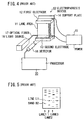
Luminous energy can be increased further by attaching a microlens array MA to the light-source side of an aperture AP. Use of the microlens array MA eliminates the need for the aperture AP since light beams are condensed onto the focal point of each microlens.
- The S/N ratio can be improved by irradiating excitation light from one side of the biochip opposite to the side where samples are arranged. Consequently, it is possible to reduce the cost of the biochip reader.
- The numerical aperture (NA) can be improved by using an immersion lens or a solid immersion lens (SIL) as the objective lens, thereby further improving the S/N ratio.
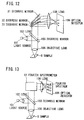
- The S/N ratio is still further improved, compared with biochip readers with a non-confocal optical system, because a confocal optical system is used with the biochip reader of the present invention.
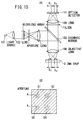
- The luminous energy of excitation light irradiated at samples increases because the anti-reflection coating is formed on one side of the substrate of the DNA chip opposite to the side where the samples are arranged. Consequently, it is possible to further improve the S/N ratio.
- Transparent electrodes have been formed on a transparent substrate. This arrangement makes it possible to accelerate hybridization by applying a positive voltage to the electrodes because DNA is charged with negative electricity.
- If samples used with the biochip reader are either DNA or RNA segments, known samples having a complementary sequence combine by hybridization with unknown samples marked with a fluorescent substance. Consequently, it is possible to identify the sequence of the unknown samples.
- If samples used with the biochip reader are either protein segments or sugar chain segments, known samples combine by antigen-antibody reaction with unknown samples. Consequently, it is possible to identify the sequence of the unknown samples.
Claims (32)
- A biochip reader for reading image data according to a plurality of samples using an optical detector by irradiating light at a biochip whereupon said plurality of samples are arranged in spots or arrays, comprising means for arranging multiple pieces of spectroscopic information of the sample under analysis in spaces among said images.
- A biochip reader as defined in claim 1, wherein said means comprises a grating, a combination of an optical filter and optical shift means, or a Fourier spectrometer, arranged between said samples and said optical detector.
- A biochip reader as defined in claim 1, wherein said means is configured so that spectroscopic information is developed on said optical detector in a two-dimensional manner if said samples are arranged in spots.
- A biochip reader as defined in claim 1, wherein said means is a scanning confocal microscope, a non-scanning confocal microscope, or a dual-grating excitation microscope.
- A biochip reader as defined in claim 1, comprising means for separating signals of said spectroscopic information from noise by using known spectra and a regression method.
- A biochip reader as defined in claim 1, wherein an aperture for restricting the area of spectroscopy is aligned with the position of each sample or with part of each sample.
- A biochip reader for reading image data according to a plurality of samples using an optical detector by irradiating light at a biochip whereupon said plurality of samples are arranged in spots or arrays, wherein reading means is a non-scanning confocal microscope having an aperture positioned to be optically conjugate with the position of the image of said sample or part of said sample in a given single image.
- A biochip reader as defined in claim 7, wherein said non-scanning confocal microscope further comprises beam-condensing means on the light-source side of said aperture.
- A biochip reader for reading image data according to a plurality of samples using an optical detector by irradiating light at a biochip whereupon said plurality of samples are arranged in spots or arrays, wherein reading means is a non-scanning confocal microscope having beamcondensing means, the focal point thereof being positioned to be optically conjugate with the position of the image of a sample or part of said sample in a given single image.
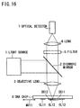
- A biochip reader comprising:a light source for emitting excitation light;a dichroic mirror for reflecting said excitation or allowing said excitation light to pass through said dichroic mirror;an objective lens for condensing light that has been reflected by or passed through said dichroic mirror onto a biochip and projecting fluorescent light produced at said biochip onto said dichroic mirror;an optical detector for detecting said fluorescent light; anda lens for condensing said fluorescent light that has been reflected by or passed through said dichroic mirror onto said optical detector,
wherein said biochip is configured using a transparent substrate allowing for passage of said excitation light and said fluorescent light and said excitation light is irradiated from one side of said biochip opposite to the side where samples are arranged. - A biochip reader as defined in claim 10, wherein said objective lens is an immersion lens.
- A biochip reader as defined in claim 10, wherein said objective lens is a water immersion lens or an oil immersion lens.
- A biochip reader as defined in claim 10, wherein said objective lens is an SIL.
- A biochip reader as defined in claim 10, wherein an optical system is a confocal optical system.
- A biochip reader as defined in claim 10, wherein an anti-reflection coating is formed on one side of said biochip opposite to the side where samples are arranged.
- A biochip reader as defined in claim 10, wherein an anti-reflection coating is formed on a surface of said transparent substrate.
- A biochip reader as defined in claim 16, wherein said anti-reflection coating is made of an indium-tin oxide film.
- A biochip reader as defined in claim 10, wherein said samples are DNA segments.
- A biochip reader as defined in claim 10, wherein said samples are RNA segments.
- A biochip reader as defined in claim 10, wherein said samples are protein segments.
- A biochip reader as defined in claim 10, wherein said samples are sugar chain segments.
- A biochip reader as defined in any of claims 1 to 9, wherein said biochip is configured using a transparent substrate allowing for passage of said excitation light and fluorescent light, and said excitation light is irradiated from one side of said biochip opposite to the side where samples are arranged.
- An electrophoresis system for conducting electrophoresis of a sample marked with fluorescent coloring matter in a lane area so that a fluorescence pattern that is produced is read, comprising:an electrophoresis unit for conducting electrophoresis by flowing a plurality of samples prepared by combining various types of target substance such as protein or DNA with different types of fluorescent coloring matter into the same lane of said lane area; anda confocal microscope or a fluorescence imaging system wherein samples in said lane area are scanned with excitation light and polychrome fluorescence patterns of said samples produced by irradiating said excitation light are simultaneously detected through a plurality of filters having different transmission characteristics,
whereby a plurality of electrophoretic patterns are detected simultaneously. - A three-dimensional electrophoresis system for conducting electrophoresis of a sample marked with fluorescent coloring matter in a lane area so that a fluorescence pattern that is produced is read, comprising:an electrophoresis unit for conducting electrophoresis by flowing various types of target substance such as protein or DNA into said lane area and applying a gradient of physical quantities such as voltage, pH, density or concentration in the direction of the depth of said sample; anda scanning confocal microscope, a non-scanning confocal microscope, or 2 photon excitation microscope, which is configured so that a sample in said lane area is scanned with excitation light and a fluorescence pattern of said sample produced by irradiating said excitation light is detected,
whereby the three-dimensional position and concentration of said sample are detected. - A three-dimensional polychrome electrophoresis system as defined in claim 24, wherein different physical gradients are applied to said electrophoresis unit of said electrophoresis system in two horizontal directions and in one vertical direction so that sample separation is performed simultaneously on all three axes.
- A three-dimensional electrophoresis system as defined in claim 24, wherein samples and markers are placed in the depth direction in said electrophoresis unit.
- A three-dimensional electrophoresis system as defined in claim 24, wherein said non-scanning confocal microscope comprises an aperture positioned to be optically conjugate with the position of the image of said sample or part of said sample in a given single image.
- A three-dimensional electrophoresis system as defined in claim 27, wherein said non-scanning confocal microscope further comprises beam-condensing means on the light-source side of said aperture.
- A three-dimensional electrophoresis system as defined in claim 24, wherein said non-scanning confocal microscope comprises beam-condensing means, the focal point thereof being positioned to be optically conjugate with the position of the image of a sample or part of said sample in a given single image.
- An electrophoresis system as defined in claim 23 or claim 24, wherein said confocal microscope has beam-condensing means on the light-source side of a confocal aperture.
- An electrophoresis system as defined in claim 24, wherein the distribution of density in the depth direction is realized by wetting only one side of a gel with a highly concentrated solution, applying a density gradient in the depth direction by means of centrifugation, or stacking multiple layers of gel with different concentrations.
- An electrophoresis system as defined in claim 24, wherein said scanning confocal microscope, non-scanning confocal microscope, or 2 photon excitation microscope, which is configured so that a sample in said lane area is scanned with excitation light and a fluorescence pattern of said sample produced by irradiating said excitation light is detected, is the biochip reader as defined in any of claims 1 to 3 or in any of claims 5 to 9.
Priority Applications (1)
| Application Number | Priority Date | Filing Date | Title |
|---|---|---|---|
| EP08160013A EP1983331B1 (en) | 1999-05-28 | 2000-05-08 | Optical system for reading a biochip |
Applications Claiming Priority (6)
| Application Number | Priority Date | Filing Date | Title |
|---|---|---|---|
| JP14940099 | 1999-05-28 | ||
| JP14940099A JP3695631B2 (en) | 1999-05-28 | 1999-05-28 | Electrophoresis device |
| JP14939999A JP3689901B2 (en) | 1999-05-28 | 1999-05-28 | Biochip reader |
| JP14939999 | 1999-05-28 | ||
| JP2000007724 | 2000-01-17 | ||
| JP2000007724A JP3859050B2 (en) | 2000-01-17 | 2000-01-17 | Biochip reader |
Related Child Applications (2)
| Application Number | Title | Priority Date | Filing Date |
|---|---|---|---|
| EP08160013A Division EP1983331B1 (en) | 1999-05-28 | 2000-05-08 | Optical system for reading a biochip |
| EP08160013.2 Division-Into | 2008-07-09 |
Publications (3)
| Publication Number | Publication Date |
|---|---|
| EP1055925A2 true EP1055925A2 (en) | 2000-11-29 |
| EP1055925A3 EP1055925A3 (en) | 2004-05-12 |
| EP1055925B1 EP1055925B1 (en) | 2010-09-08 |
Family
ID=27319743
Family Applications (2)
| Application Number | Title | Priority Date | Filing Date |
|---|---|---|---|
| EP00109722A Expired - Lifetime EP1055925B1 (en) | 1999-05-28 | 2000-05-08 | Biochip reader |
| EP08160013A Expired - Lifetime EP1983331B1 (en) | 1999-05-28 | 2000-05-08 | Optical system for reading a biochip |
Family Applications After (1)
| Application Number | Title | Priority Date | Filing Date |
|---|---|---|---|
| EP08160013A Expired - Lifetime EP1983331B1 (en) | 1999-05-28 | 2000-05-08 | Optical system for reading a biochip |
Country Status (3)
| Country | Link |
|---|---|
| US (2) | US20040182710A1 (en) |
| EP (2) | EP1055925B1 (en) |
| DE (2) | DE1055925T1 (en) |
Cited By (14)
| Publication number | Priority date | Publication date | Assignee | Title |
|---|---|---|---|---|
| DE10131687A1 (en) * | 2001-06-29 | 2003-01-16 | Eppendorf Ag | Device for carrying out nucleic acid amplification reactions while simultaneously monitoring the formation of amplification products |
| EP1283416A2 (en) * | 2001-08-09 | 2003-02-12 | Yokogawa Electric Corporation | Biochip reader and fluorometric imaging apparatus |
| EP1388587A1 (en) * | 2001-05-11 | 2004-02-11 | Matsushita Electric Industrial Co., Ltd. | Biomolecular substrate and method and apparatus for examination and diagnosis using the same |
| US6864976B2 (en) * | 2001-05-10 | 2005-03-08 | Yokogawa Electric Corporation | Biochip reader |
| DE102004015488A1 (en) * | 2004-03-26 | 2005-10-20 | Lavision Biotec Gmbh | Method for reading out by strip-scanning of flat objects with substances that emit fluorescence radiation |
| DE102006058575B4 (en) * | 2005-12-12 | 2009-01-15 | Combisep Inc., Ames | Multiplex CE fluorescence system |
| WO2010121643A1 (en) * | 2009-04-20 | 2010-10-28 | Agilent Technologies, Inc. | Identifying calibration markers in multiple detection channels |
| CN102818886A (en) * | 2012-08-28 | 2012-12-12 | 天津市先石光学技术有限公司 | Low-dose homogenous excitation light immunoassay instrument |
| DE102014111167A1 (en) * | 2014-08-06 | 2016-02-11 | Carl Zeiss Microscopy Gmbh | High-resolution scanning microscopy with the distinction of at least two wavelength ranges |
| CN105424698A (en) * | 2015-11-25 | 2016-03-23 | 江苏三联生物工程有限公司 | Biochip reading instrument with gripper function |
| CN108235730A (en) * | 2018-01-09 | 2018-06-29 | 深圳达闼科技控股有限公司 | Micro spectral detection device |
| EP1996922B1 (en) * | 2006-03-22 | 2018-11-21 | Crimson International Assets LLC | Fluorescence reader |
| CN112684600A (en) * | 2019-10-19 | 2021-04-20 | 美国赛库莱特生物有限公司 | Microscope for positioning structures on the inner surface of a fluid channel |
| CN114270176A (en) * | 2019-09-11 | 2022-04-01 | 松下知识产权经营株式会社 | Moisture sensing device |
Families Citing this family (24)
| Publication number | Priority date | Publication date | Assignee | Title |
|---|---|---|---|---|
| US20040112535A1 (en) * | 2000-04-13 | 2004-06-17 | Olympus Optical Co., Ltd. | Focus detecting device |
| JP4701739B2 (en) * | 2005-02-17 | 2011-06-15 | パナソニック株式会社 | Fluorescence measuring device |
| US7817273B2 (en) * | 2005-06-30 | 2010-10-19 | Life Technologies Corporation | Two-dimensional spectral imaging system |
| US7663750B2 (en) | 2005-06-30 | 2010-02-16 | Applied Biosystems, Llc | Two-dimensional spectral imaging system |
| US7805081B2 (en) * | 2005-08-11 | 2010-09-28 | Pacific Biosciences Of California, Inc. | Methods and systems for monitoring multiple optical signals from a single source |
| US7518728B2 (en) * | 2005-09-30 | 2009-04-14 | Intel Corporation | Method and instrument for collecting fourier transform (FT) Raman spectra for imaging applications |
| US7692783B2 (en) * | 2006-02-13 | 2010-04-06 | Pacific Biosciences Of California | Methods and systems for simultaneous real-time monitoring of optical signals from multiple sources |
| US20080277595A1 (en) * | 2007-05-10 | 2008-11-13 | Pacific Biosciences Of California, Inc. | Highly multiplexed confocal detection systems and methods of using same |
| US20100167413A1 (en) * | 2007-05-10 | 2010-07-01 | Paul Lundquist | Methods and systems for analyzing fluorescent materials with reduced autofluorescence |
| US20090262332A1 (en) * | 2008-04-18 | 2009-10-22 | Microvast, Inc. | High-throughput spectral imaging and spectroscopy apparatus and methods |
| EP2291643B1 (en) * | 2008-06-24 | 2016-11-23 | Koninklijke Philips N.V. | Microarray characterization system and method |
| EP2163885A1 (en) * | 2008-06-24 | 2010-03-17 | Koninklijke Philips Electronics N.V. | Microarray characterization system and method |
| US8275226B2 (en) | 2008-12-09 | 2012-09-25 | Spectral Applied Research Ltd. | Multi-mode fiber optically coupling a radiation source module to a multi-focal confocal microscope |
| US8357281B2 (en) * | 2009-09-21 | 2013-01-22 | Advanced Analytical Technologies, Inc. | Multi-wavelength fluorescence detection system for multiplexed capillary electrophoresis |
| US8670178B2 (en) * | 2009-12-08 | 2014-03-11 | Spectral Applied Research Inc. | Imaging distal end of multimode fiber |
| US9274042B2 (en) | 2010-05-07 | 2016-03-01 | Stc.Unm | Spatially correlated light collection from multiple sample streams excited with a line focused light source |
| US8830451B1 (en) | 2010-05-07 | 2014-09-09 | Stc.Unm | Multinode acoustic focusing for parallel flow cytometry analysis applications |
| US9074977B2 (en) | 2010-05-07 | 2015-07-07 | Stc.Unm | Multinode acoustic focusing for parallel flow cytometry analysis applications |
| DE102011083718A1 (en) * | 2011-09-29 | 2013-04-04 | Siemens Aktiengesellschaft | Confocal spectrometer and method of imaging in a confocal spectrometer |
| WO2013191772A1 (en) * | 2012-06-21 | 2013-12-27 | Stc.Unm | Spatially correlated light collection from multiple sample streams excited with a line focused light source |
| WO2014194028A1 (en) * | 2013-05-31 | 2014-12-04 | Pacific Biosciences Of California, Inc | Analytical devices having compact lens train arrays |
| CN104568893A (en) * | 2015-01-24 | 2015-04-29 | 北京中拓机械集团有限责任公司 | High-speed fluorescence spectrum detection device for semiconductor wafer |
| CN106841137B (en) * | 2017-01-10 | 2020-06-19 | 清华大学 | Method and system for multi-color fluorescence imaging under single exposure |
| US10883820B2 (en) * | 2017-11-13 | 2021-01-05 | Taiwan Semiconductor Manufacturing Co., Ltd. | Apparatus and method for metrology |
Citations (9)
| Publication number | Priority date | Publication date | Assignee | Title |
|---|---|---|---|---|
| WO1993017325A1 (en) * | 1992-02-24 | 1993-09-02 | The Regents Of The University Of California | Capillary array confocal fluorescence scanner and method |
| WO1994027137A2 (en) * | 1993-05-18 | 1994-11-24 | University Of Utah Research Foundation | Apparatus and methods for multianalyte homogeneous fluoroimmunoassays |
| US5538613A (en) * | 1993-10-26 | 1996-07-23 | Genesys Technologies, Inc. | Electrophoresis analyzer |
| US5751417A (en) * | 1995-03-20 | 1998-05-12 | Uhl; Rainer | Arrangement for confocal fluorescence microscopy |
| US5834758A (en) * | 1994-09-02 | 1998-11-10 | Affymetrix, Inc. | Method and apparatus for imaging a sample on a device |
| WO1998051823A1 (en) * | 1997-05-16 | 1998-11-19 | Mosaic Technologies | Electrophoretic analysis of molecules using immobilized probes |
| US5859700A (en) * | 1995-11-22 | 1999-01-12 | Kairos Scientific, Inc. | High resolution imaging microscope (HIRIM) and uses thereof |
| US5871628A (en) * | 1996-08-22 | 1999-02-16 | The University Of Texas System | Automatic sequencer/genotyper having extended spectral response |
| WO1999023474A1 (en) * | 1997-10-31 | 1999-05-14 | Carl Zeiss | Optical array system and reader for micro titer plates |
Family Cites Families (13)
| Publication number | Priority date | Publication date | Assignee | Title |
|---|---|---|---|---|
| US4790919A (en) * | 1984-06-28 | 1988-12-13 | E. I. Du Pont De Nemours And Company | Process for preparation of electrophoresis gel material |
| EP0217619A3 (en) | 1985-09-26 | 1989-01-25 | Molecular Devices Corporation | Apparatus and method for optical assay imaging |
| US5038352A (en) * | 1990-11-13 | 1991-08-06 | International Business Machines Incorporation | Laser system and method using a nonlinear crystal resonator |
| US5324633A (en) * | 1991-11-22 | 1994-06-28 | Affymax Technologies N.V. | Method and apparatus for measuring binding affinity |
| US5422712A (en) * | 1992-04-01 | 1995-06-06 | Toa Medical Electronics Co., Ltd. | Apparatus for measuring fluorescent spectra of particles in a flow |
| US6108135A (en) * | 1997-06-16 | 2000-08-22 | Digital Papyrus Corporation | Planar proximity lens element and disk drive using same |
| US6100535A (en) * | 1998-01-29 | 2000-08-08 | The Regents Of The University Of California | Rotary confocal scanner for detection of capillary arrays |
| US6100541A (en) * | 1998-02-24 | 2000-08-08 | Caliper Technologies Corporation | Microfluidic devices and systems incorporating integrated optical elements |
| US6406921B1 (en) * | 1998-07-14 | 2002-06-18 | Zyomyx, Incorporated | Protein arrays for high-throughput screening |
| US6603537B1 (en) * | 1998-08-21 | 2003-08-05 | Surromed, Inc. | Optical architectures for microvolume laser-scanning cytometers |
| US6642062B2 (en) * | 1998-09-03 | 2003-11-04 | Trellis Bioinformatics, Inc. | Multihued labels |
| JP2000147421A (en) * | 1998-11-17 | 2000-05-26 | Yokogawa Electric Corp | Confocal optical scanner |
| WO2001069211A1 (en) * | 2000-03-16 | 2001-09-20 | Spectrumedix Corporation | Multi-wavelength array reader for biological assay |
-
2000
- 2000-05-08 EP EP00109722A patent/EP1055925B1/en not_active Expired - Lifetime
- 2000-05-08 DE DE1055925T patent/DE1055925T1/en active Pending
- 2000-05-08 EP EP08160013A patent/EP1983331B1/en not_active Expired - Lifetime
- 2000-05-08 DE DE60044923T patent/DE60044923D1/en not_active Expired - Lifetime
-
2004
- 2004-01-30 US US10/769,017 patent/US20040182710A1/en not_active Abandoned
- 2004-01-30 US US10/768,632 patent/US20040184960A1/en not_active Abandoned
Patent Citations (9)
| Publication number | Priority date | Publication date | Assignee | Title |
|---|---|---|---|---|
| WO1993017325A1 (en) * | 1992-02-24 | 1993-09-02 | The Regents Of The University Of California | Capillary array confocal fluorescence scanner and method |
| WO1994027137A2 (en) * | 1993-05-18 | 1994-11-24 | University Of Utah Research Foundation | Apparatus and methods for multianalyte homogeneous fluoroimmunoassays |
| US5538613A (en) * | 1993-10-26 | 1996-07-23 | Genesys Technologies, Inc. | Electrophoresis analyzer |
| US5834758A (en) * | 1994-09-02 | 1998-11-10 | Affymetrix, Inc. | Method and apparatus for imaging a sample on a device |
| US5751417A (en) * | 1995-03-20 | 1998-05-12 | Uhl; Rainer | Arrangement for confocal fluorescence microscopy |
| US5859700A (en) * | 1995-11-22 | 1999-01-12 | Kairos Scientific, Inc. | High resolution imaging microscope (HIRIM) and uses thereof |
| US5871628A (en) * | 1996-08-22 | 1999-02-16 | The University Of Texas System | Automatic sequencer/genotyper having extended spectral response |
| WO1998051823A1 (en) * | 1997-05-16 | 1998-11-19 | Mosaic Technologies | Electrophoretic analysis of molecules using immobilized probes |
| WO1999023474A1 (en) * | 1997-10-31 | 1999-05-14 | Carl Zeiss | Optical array system and reader for micro titer plates |
Non-Patent Citations (1)
| Title |
|---|
| L. R. BREWER: "three-dimensional imaging of DNA fragments during electrophoresis using a confocal detector" ELECTROPHORESIS, vol. 16, 1995, pages 1846-1850, XP008028747 * |
Cited By (25)
| Publication number | Priority date | Publication date | Assignee | Title |
|---|---|---|---|---|
| US6864976B2 (en) * | 2001-05-10 | 2005-03-08 | Yokogawa Electric Corporation | Biochip reader |
| EP1650553A3 (en) * | 2001-05-10 | 2006-08-23 | Yokogawa Electric Corporation | Biochip reader |
| EP1650551A3 (en) * | 2001-05-10 | 2006-05-17 | Yokogawa Electric Corporation | Biochip Reader |
| US7833701B2 (en) | 2001-05-11 | 2010-11-16 | Panasonic Corporation | Biomolecule substrate, and test and diagnosis methods and apparatuses using the same |
| EP1388587A1 (en) * | 2001-05-11 | 2004-02-11 | Matsushita Electric Industrial Co., Ltd. | Biomolecular substrate and method and apparatus for examination and diagnosis using the same |
| EP1388587A4 (en) * | 2001-05-11 | 2006-12-06 | Matsushita Electric Ind Co Ltd | Biomolecular substrate and method and apparatus for examination and diagnosis using the same |
| US8691560B2 (en) | 2001-05-11 | 2014-04-08 | Panasonic Corporation | Biomolecule substrate, and test and diagnosis methods and apparatuses using the same |
| DE10131687A1 (en) * | 2001-06-29 | 2003-01-16 | Eppendorf Ag | Device for carrying out nucleic acid amplification reactions while simultaneously monitoring the formation of amplification products |
| EP1283416A2 (en) * | 2001-08-09 | 2003-02-12 | Yokogawa Electric Corporation | Biochip reader and fluorometric imaging apparatus |
| DE102004015488B4 (en) * | 2004-03-26 | 2008-01-31 | Lavision Biotec Gmbh | Method for reading out by strip-scanning of flat objects with substances that emit fluorescence radiation |
| DE102004015488A1 (en) * | 2004-03-26 | 2005-10-20 | Lavision Biotec Gmbh | Method for reading out by strip-scanning of flat objects with substances that emit fluorescence radiation |
| US7211807B2 (en) | 2004-03-26 | 2007-05-01 | Lavision Biotec Gmbh | Readout method performed by stripe scanning planar objects with substances emitting fluorescence radiation |
| DE102006058575B4 (en) * | 2005-12-12 | 2009-01-15 | Combisep Inc., Ames | Multiplex CE fluorescence system |
| EP1996922B1 (en) * | 2006-03-22 | 2018-11-21 | Crimson International Assets LLC | Fluorescence reader |
| WO2010121643A1 (en) * | 2009-04-20 | 2010-10-28 | Agilent Technologies, Inc. | Identifying calibration markers in multiple detection channels |
| CN102818886A (en) * | 2012-08-28 | 2012-12-12 | 天津市先石光学技术有限公司 | Low-dose homogenous excitation light immunoassay instrument |
| DE102014111167A1 (en) * | 2014-08-06 | 2016-02-11 | Carl Zeiss Microscopy Gmbh | High-resolution scanning microscopy with the distinction of at least two wavelength ranges |
| US11204489B2 (en) | 2014-08-06 | 2021-12-21 | Carl Zeiss Microscopy Gmbh | High-resolution scanning microscopy with discrimination between at least two wavelength ranges |
| CN105424698A (en) * | 2015-11-25 | 2016-03-23 | 江苏三联生物工程有限公司 | Biochip reading instrument with gripper function |
| CN105424698B (en) * | 2015-11-25 | 2018-05-15 | 江苏三联生物工程有限公司 | A kind of biological chip reading apparatus with handgrip function |
| CN108235730A (en) * | 2018-01-09 | 2018-06-29 | 深圳达闼科技控股有限公司 | Micro spectral detection device |
| WO2019136579A1 (en) * | 2018-01-09 | 2019-07-18 | 深圳达闼科技控股有限公司 | Miniature spectral detection apparatus |
| CN114270176A (en) * | 2019-09-11 | 2022-04-01 | 松下知识产权经营株式会社 | Moisture sensing device |
| CN112684600A (en) * | 2019-10-19 | 2021-04-20 | 美国赛库莱特生物有限公司 | Microscope for positioning structures on the inner surface of a fluid channel |
| CN112684600B (en) * | 2019-10-19 | 2022-06-03 | 美国赛库莱特生物有限公司 | Microscope for positioning structures on the inner surface of a fluid channel |
Also Published As
| Publication number | Publication date |
|---|---|
| DE60044923D1 (en) | 2010-10-21 |
| EP1983331A3 (en) | 2008-11-05 |
| EP1983331B1 (en) | 2011-07-13 |
| EP1983331A2 (en) | 2008-10-22 |
| EP1055925B1 (en) | 2010-09-08 |
| EP1055925A3 (en) | 2004-05-12 |
| US20040182710A1 (en) | 2004-09-23 |
| DE1055925T1 (en) | 2001-06-07 |
| US20040184960A1 (en) | 2004-09-23 |
Similar Documents
| Publication | Publication Date | Title |
|---|---|---|
| EP1055925A2 (en) | Biochip reader and electrophoresis system | |
| US8264680B2 (en) | Biochip reader and electrophoresis system | |
| EP1837647B1 (en) | Multiplexed capillary electrophoresis method | |
| US6704104B2 (en) | Multi-wavelength array reader for biological assay | |
| JP5174035B2 (en) | 2D array imaging | |
| EP2309253A2 (en) | Apparatus for reading signals generated from resonance light scattered particle labels | |
| US20050213093A1 (en) | Time-delay integration in electrophoretic detection systems | |
| US5556529A (en) | DNA base sequencer | |
| WO1998049543A1 (en) | Scanning optical detection system | |
| JPH09288088A (en) | Capillary array electrophoretic apparatus | |
| Barsky et al. | Fluorescence data analysis on gel-based biochips | |
| EP0294524A1 (en) | Real time scanning electrophoresis apparatus for DNA sequencing | |
| JP2001311690A (en) | Biochip reader and electrophoretic apparatus | |
| EP0911630A1 (en) | Fluorescence detector | |
| CA2284195A1 (en) | Device and method for capillary electrophoresis | |
| JP3695631B2 (en) | Electrophoresis device | |
| JPH0814537B2 (en) | Real-time scanning electrophoresis apparatus for DNA sequencing | |
| JP2011002398A (en) | Spectroscopic imaging device | |
| AU2002322688A1 (en) | Time-delay integration in electrophoretic detection systems | |
| EP1682883A1 (en) | Methods and devices for measuring fluorescence of a sample in a capillary |
Legal Events
| Date | Code | Title | Description |
|---|---|---|---|
| PUAI | Public reference made under article 153(3) epc to a published international application that has entered the european phase |
Free format text: ORIGINAL CODE: 0009012 |
|
| AK | Designated contracting states |
Kind code of ref document: A2 Designated state(s): AT BE CH CY DE DK ES FI FR GB GR IE IT LI LU MC NL PT SE |
|
| AX | Request for extension of the european patent |
Free format text: AL;LT;LV;MK;RO;SI |
|
| TCNL | Nl: translation of patent claims filed | ||
| DET | De: translation of patent claims | ||
| PUAL | Search report despatched |
Free format text: ORIGINAL CODE: 0009013 |
|
| AK | Designated contracting states |
Kind code of ref document: A3 Designated state(s): AT BE CH CY DE DK ES FI FR GB GR IE IT LI LU MC NL PT SE |
|
| AX | Request for extension of the european patent |
Extension state: AL LT LV MK RO SI |
|
| 17P | Request for examination filed |
Effective date: 20040727 |
|
| AKX | Designation fees paid |
Designated state(s): DE GB NL |
|
| 17Q | First examination report despatched |
Effective date: 20080125 |
|
| GRAP | Despatch of communication of intention to grant a patent |
Free format text: ORIGINAL CODE: EPIDOSNIGR1 |
|
| RTI1 | Title (correction) |
Free format text: BIOCHIP READER |
|
| GRAS | Grant fee paid |
Free format text: ORIGINAL CODE: EPIDOSNIGR3 |
|
| GRAA | (expected) grant |
Free format text: ORIGINAL CODE: 0009210 |
|
| AK | Designated contracting states |
Kind code of ref document: B1 Designated state(s): DE GB NL |
|
| REG | Reference to a national code |
Ref country code: GB Ref legal event code: FG4D |
|
| REF | Corresponds to: |
Ref document number: 60044923 Country of ref document: DE Date of ref document: 20101021 Kind code of ref document: P |
|
| REG | Reference to a national code |
Ref country code: NL Ref legal event code: T3 |
|
| PLBE | No opposition filed within time limit |
Free format text: ORIGINAL CODE: 0009261 |
|
| STAA | Information on the status of an ep patent application or granted ep patent |
Free format text: STATUS: NO OPPOSITION FILED WITHIN TIME LIMIT |
|
| 26N | No opposition filed |
Effective date: 20110609 |
|
| REG | Reference to a national code |
Ref country code: DE Ref legal event code: R097 Ref document number: 60044923 Country of ref document: DE Effective date: 20110609 |
|
| PGFP | Annual fee paid to national office [announced via postgrant information from national office to epo] |
Ref country code: NL Payment date: 20140410 Year of fee payment: 15 |
|
| REG | Reference to a national code |
Ref country code: NL Ref legal event code: MM Effective date: 20150601 |
|
| PG25 | Lapsed in a contracting state [announced via postgrant information from national office to epo] |
Ref country code: NL Free format text: LAPSE BECAUSE OF NON-PAYMENT OF DUE FEES Effective date: 20150601 |
|
| PGFP | Annual fee paid to national office [announced via postgrant information from national office to epo] |
Ref country code: GB Payment date: 20160504 Year of fee payment: 17 Ref country code: DE Payment date: 20160504 Year of fee payment: 17 |
|
| REG | Reference to a national code |
Ref country code: DE Ref legal event code: R119 Ref document number: 60044923 Country of ref document: DE |
|
| GBPC | Gb: european patent ceased through non-payment of renewal fee |
Effective date: 20170508 |
|
| PG25 | Lapsed in a contracting state [announced via postgrant information from national office to epo] |
Ref country code: GB Free format text: LAPSE BECAUSE OF NON-PAYMENT OF DUE FEES Effective date: 20170508 Ref country code: DE Free format text: LAPSE BECAUSE OF NON-PAYMENT OF DUE FEES Effective date: 20171201 |