FIELD OF THE INDUSTRIAL UTILIZATION
The present invention relates to a gas discharge panel
and a method for manufacturing the same.
In particular, the present invention relates to a gas discharge panel of the type
comprising the features set out in the preamble clause of claim 1. A similar type of gas
discharge panel is known from WO 95/19027A.
BACKGROUND OF THE INVENTION
An AC type plasma display panel (hereinafter called
the PDP) as shown in Fig.7 has been known as an example of
gas discharge panel.
Panel configuration and operation of the conventional
PDP will be described below with reference to the
accompanying drawing.
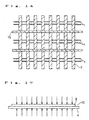
Fig.20 is a perspective sectional view schematically
showing the PDP of the prior art.
In this drawing, reference numeral 4 denotes a front
substrate (also called the upper panel substrate), and 8
denotes a back substrate (also called the lower panel
substrate). An outer casing 10 has such a configuration that
the front substrate 4 and the back substrate 8 are disposed
to oppose each other with the gap between the peripheries
thereof being filled with a sealing member 9 (refer to
Fig.21) made of glass having a low melting point thereby
to form a gas discharge space which is sealed to be airtight
and is filled with a rare gas (a mixture of helium and xenon
gases) with a pressure from 4 x 10⁴ to 7 x 10⁴ Pa (300 to 500 Torr).
The front substrate 4 comprises a front panel glass
201, display electrodes 1 formed in a pattern on the front
panel glass 201, a dielectric film 2 formed to cover the
display electrodes 1 and an MgO protective film 3 formed
on the dielectric film 2.
The back substrate 8 comprises a back panel glass 202,
address electrodes 5 (also called the data electrode) formed
in a pattern on the surface of the back panel glass 202,
a dielectric film 6 formed to cover the address electrodes,
division walls 7 comprising a plurality of ribs, and RGB
fluorescent substances 11a through 11c applied between the
ribs. The division wall 7 is means for dividing the gas
discharge space. Compartment 12 thus divided serve as light
emitting regions, while the fluorescent substance 11 is
coated separately in each of these light emitting regions.
The ribs of the division walls 7 and the address electrodes
5 are formed in parallel with each other and the display
electrodes 1 and the address electrodes 5 cross at right
angles with each other.
In the casing 10 configured as described above, when
voltages are applied to the address electrodes 5 and the
display electrodes 1 at a proper timing, discharge occurs
in the compartment 12 divided by the division walls 7
corresponding to display pixels so that ultraviolet rays
are emitted and excite the RGB fluorescent substances 11a
through 11c that in turn emit visible light which constitutes
an image.
The front panel glass and the back panel glass are
sealed to form a space delimited thereby that is filled with
the discharge gas. Because pressure of the discharge gas
filling the space is usually lower than the atmospheric
pressure, however, the front panel glass and the back panel
glass are pressed inward by the atmospheric pressure so that
ridges of the division walls 7, or top portions of the ribs,
make contact with the inner surface of the front panel glass
201, thereby keeping the clearance between the front panel
glass 201 and the hack panel glass 202. As a consequence,
it is not necessary to bond the ridges of the division walls
7 and the inner surface of the front panel glass 201, which
are merely brought into contact with each other.
Now a method for manufacturing the PDP of the prior
art will be described below with reference to the
accompanying drawings.
Fig.21 is a partially cutaway perspective view
schematically showing the same PDP of the prior art as shown
in Fig.20.
As shown in Fig.21, the front substrate 4 is made by
forming the electrodes 1 on the glass substrate 201, forming
the dielectric film 2 to cover the electrodes 1, firing the
dielectric film 2 and forming the protective film (MgO) 3
thereon by EB vapor deposition.
As for the back substrate 8, the electrodes 5 are
formed on a glass substrate 202 and is then covered the
dielectric film 6 formed thereon and fired. Then after
forming a layer of a material to make the division walls
all over the surface by printing process, the division wall
material is removed by sand blast from portions where the
division wall is not to be formed thereby to form the division
walls 7 in linear configuration through a firing process.
Then the space between the ribs of the division walls 7 is
filled with the fluorescent substance 11 by a printing
process or the like, dried and fired to complete the back
substrate 8.
The front substrate 4 and the back substrate 8
completed as described above are fired after applying glass
of low melting point that makes the sealing member 9 to the
peripheries thereof, thereby sealing the space therebetween.
After evacuating the inner space through a chip tube (also
called the piping member) 13, the space is filled with a
rare gas and the tube is chipped off, thereby completing
the PDP.
Operations of filling the inner space with the rare
gas using the chip tube 13 and chipping off will be described
in more detail below with reference to Figs.21, 22.
As shown in Fig.21, when manufacturing the PDP
(container filled with the gas) of the prior art, the lower
panel substrate 8 is fitted on an external position thereof
with the piping member 13 that communicates with the gas
discharge space in the casing 10 via a through hole 8a formed
in the lower panel substrate 8. Then after purging the air
from the inside of the casing (the container before being
filled with the gas) 10 and filling the inner space with
the discharge gas, the piping member 13 is closed thereby
sealing the inner space of the casing 10.
Closing of the piping member 13 is carried out as shown
in Fig.22(a) by heating and melting the closing portion 13a
of the piping member 13 with a gas burner 14 or the like
applied from the outside. After causing the piping member
13 to contract by moving the lower portion of the closing
portion 13a which has melted away from the casing 10 as shown
in Fig.22(b), the piping member 13 is cut off by melting
as shown in Fig.22(c). Thus in the prior art, since the
atmospheric pressure is higher than the inner pressure of
the casing 10, the closing portion 13a of the piping member
13 which has contracted is completely closed due to
contraction of the inner wall of the piping.
The lower panel substrate 8 bears the piping member
13, that was used when purging air from the inner space of
the casing 10 and filling it with the discharge gas,
remaining thereon as bonded by using the same material as
the sealing member 9.
In the PDP configuration of the prior art as described
above, however, the front substrate 4 and the back substrate
8 are bonded to each other on the peripheries thereof by
frit glass (sealing member 9) used for sealing but mostly
secured'by the differential pressure between the
atmospheric pressure acting thereon from the outside and
the inner pressure which is below one atmosphere of the gas
filing the space between the front substrate and the back
substrate, that causes the front substrate to be pressed
against the division walls thereby to maintain the
configuration.
Pressure of the filling gas is generally from 4 x 10⁴ to 7 x 10⁴ Pa (300 Torr
to 500 Torr), which is not significantly different from the
atmospheric pressure of 1 x 10⁵ Pa (760 Torr).
As a consequence, there has been such a problem that,
when the PDP of the prior art is used onboard an airplane,
for example, such a flight condition as the pressure in the
airplane drops significantly below the normal atmospheric
pressure causes the inner surface of the front substrate
comes off the ridges of the division walls at the middle
of the PDP, thus resulting in cross talk.
Even at the normal atmospheric pressure, there has
been such a problem that, when the PDP is subject to vibration,
the front substrate temporarily comes off the division walls
thus resulting in cross talk leading to disturbed image.
Thus the PDP of the prior art configuration has
problems such as the displayed image is disturbed due to
vibration when used onboard vehicles such as trains and
buses.
Moreover, manufacture of the PDP of the prior art
involves many firing processes that require a significant
number of electric furnaces, leading to high energy cost
and making it difficult to achieve energy-efficient
production.
The PDP of the prior art configuration has also such
a problem that satisfactory brightness cannot necessarily
be achieved. In order to improve the brightness, it is
believed that the inner pressure of the discharge gas filing
the inside of the casing 10 must be increased to a level
above 7 x 10⁴ Pa (500 Torr).
In the prior art configuration, however, increasing
the inner pressure of the discharge gas filing the inside
of the casing 10 to a level of about 1 to 1.33 x 10⁵ Pa (760 Torr to 1000 Torr)
causes a gap to be generated between the ridges of the
division walls 7 formed on the lower panel substrate 8 and
the upper panel substrate 4, or the upper panel substrate
4 and the lower panel substrate 8 to swell outwardly.
As a consequence, there has been such a problem that
isolation of the adjacent compartments 12 divided by the
ribs of the division walls 7 is broken by the gap, resulting
in deterioration in the quality of display by the PDP such
as cross talk. Also in case the inner pressure of the
discharge gas filling the inside of the casing 10 is near
equal to or above the atmospheric pressure, the sealing
method that makes use of the atmospheric pressure which is
higher than the filling gas pressure as described in
conjunction with the conventional manufacturing method can
no longer be employed.
Prior art WO 95/19027A mentioned above describes a method of manufacturing such a
gas discharge display where the planar substrates are bonded to the division walls by a
wafer bonding process
so as to provide individual cavities which are
filled with gas discharge materials, whereby the
pressure within such a cavity can be
substantially more than 1 x 10⁵ Pa (1 atm).
DISCLOSURE OF THE INVENTION
An object of the present invention is to solve the
problems of the plasma display panel of the prior art
described above and provide a gas discharge panel that is
less prone to cross talk and is capable of producing more
stable image than the prior art, and a method for
manufacturing the same.
Another object of the present invention is to solve
the problems of the method for manufacturing the plasma
display panel of the prior art described above, and provide
a method for manufacturing a gas discharge panel that is
capable of reducing the number of firing processes over the
prior art.
Another object of the present invention is to solve
the problems of the plasma display panel of the prior art
described above and provide a gas discharge panel that is
capable of achieving higher brightness than the prior art,
and a method for manufacturing the same.
The present invention achieves its objects by providing a gas discharge panel comprising
the features set out in independent claim 1.
The present invention also provides a method of manufacturing a gas discharge panel
comprising the features of claim 1 by the method claimed in independent claim 17.
Specific embodiments of the invention are claimed in the dependent claims.
The gas discharge panel comprising:
wherein ridges of said division walls are bonded onto the
inner surface of said first panel substrate via
bonding members.
According to one embodiment, the bonding member used in the bonding process
includes a light-transmitting material.
According to another embodiment, the bonding member used in the bonding process
includes a light-absorbing material, and the material for
making said division wall includes a light-reflecting
material.
According to another embodiment, the width of bonding portion between the
ridge of said division wall and said first panel substrate
is controlled so that the bonding portion does not intrude
into a light emitting region in the divided gas discharge
space.
According to a further embodiment, the bonding member used in the bonding process
includes fusible glass.
According to another embodiment, the softening point of said bonding member is lower
than the softening point of said division walls.
The difference in the softening point of said bonding
member and said division walls is not lower than 20 °C and
not higher than 200°C.
According to the embodiment where the bonding member
includes fusible glass, the division walls have holes on the ridges
thereof and said bonding members infiltrates the holes.
The division walls may be formed by thermal
spray process.
Further, at least one of the ridge surface of said
division walls and portions of the inner surface of said
first panel substrate bonded to the ridges has irregular
shape.
According to a further embodiment of the invention all or a part of the ridges of said division walls
are bonded onto the inner surface of said first panel
substrate.
According to this embodiment, said division walls are a plurality of long
plate-shaped ribs disposed in parallel to each other, and
the bonding is achieved by using bonding members formed
linearly in a direction substantially at right angles with
the longitudinal direction of said ribs.
Also, according to this embodiment, said bonding member includes a light-absorbing
material.
Further, according to this same embodiment, said first panel substrate includes first electrodes, and notation that part of the ridges of
said division walls are bonded onto the inner surface of
said first panel substrate means that said bonding is
provided in the vicinity of said first electrode in the
ridges of said division walls.
According to another embodiment of the invention,
the ridges of said division walls have recesses
formed thereon, and said bonding is achieved by using said
recesses.
According to another embodiment of the invention,
said division walls and said second panel substrate
are bonded by using frit glass.
The present invention also provides a method for manufacturing a gas discharge
panel as claimed in
claim 1, the method comprising the steps of:
According to one embodiment of this method, said assembling step to form the gas
discharge panel is carried out by pressurizing said first panel substrate (4) and/or said
second panel substrate (8) that oppose each other so that a pressure is applied at least to
the portions where said bonding members (15) are provided.
According to this embodiment, the
pressurization may be carried out by utilizing the resilience
of a spring member.
The
pressurization may also be carried out by utilizing the weight of
a plate.
The
pressurization may also be carried out by interposing a shock
absorber between said plate and said panel substrate
According to another embodiment of this method,
said bonding member includes fusible glass, an organic
binder and an organic solvent which is applied to the ridges
of said division walls and/or the inner surface of said
first panel substrate; and said method includes
a heating process of heating the bonding member which has
been applied to a temperature not lower than the melting
point of the fusible glass.
According to this method,
a temporary firing process may be provided between said
application process and said heating process for heating
said bonding member to such an extent as most of the
organic binder and of the organic solvent included in the
applied bonding member are removed; and
the assembly process is provided between said temporary firing
process and said heating process for assembling said
first panel substrate and said second panel substrate
into said gas discharge panel by means of said sealing
portion.
According to another embodiment of the method of
the present invention,
the manufacturing method further comprises:
wherein the division wall forming process comprises:
- a first process of providing a mask member having a
predetermined opening on said panel substrate; and
- a second process of providing said division wall forming
material in said opening, and the bonding member
attaching process comprises:
- a third process of disposing said bonding member on the
ridges of said division walls formed in said second
process by using said mask member; and
- a fourth process of removing the mask member
According to this embodiment, a thermal spray
method is employed in said second process and/or said third
process.
According to this embodiment, said
mask member includes a photosensitive material.
Further, according to this embodiment, said mask
member is a photosensitive resin film.
According to this embodiment, said
division wall material includes fusible glass, and firing
of said division walls and firing of said bonding member
are carried out in the same process.
According to another embodiment of the method of the present invention the method includes
a division wall forming process of forming said division
walls on said second panel substrate;
said attaching process applies fusible glass paste as said bonding member to
the ridges of said division walls; and includes
a firing process of firing the fusible glass paste,
wherein
part of said division walls have light reflectivity and said
fusible glass paste has light absorbency, and
wherein
said firing process is a process of bonding the ridges of
said division walls and the inner surface of the first panel
substrate by using said fusible glass paste.
According to another embodiment of said method for manufacturing the gas
discharge panel, said
attaching process employs a screen printing method.
Further, a screen mask
used in said screen printing method does not have a pattern.
According to another embodiment of said method for manufacturing a gas discharge
panel,
said first panel substrate has first electrodes;
said second panel substrate has second electrodes and
opposes said first panel substrate; and comprises
a process of forming grooves by exposing a photosensitive
material provided on said second panel substrate to
light; and
a thermal spray process of filling the grooves formed in
the foregoing process with a dielectric material
to form said division
walls, followed by thermal spraying frit glass onto said division walls
to form the bonding members,
while coolant gas is caused to flow along the material
ejected from a thermal spray nozzle to cool down the
second panel substrate in said thermal spray process.
According to this embodiment, said gas
discharge panel has a dielectric film that covers said second
electrodes and the material making said dielectric film and
said division walls is alumina.
According to an embodiment of the method for manufacturing the gas
discharge panel of the present invention, said piping
member is closed by heating said piping member and pressing
said piping member from the outside toward the inside so
that the piping member is blocked in the sealing process.
According to another embodiment,
the piping
member is closed by heating said piping member to melt a
sealing member housed in the piping member so that the piping
member is blocked in the sealing process.
According to yet another embodiment,
the piping
member is closed by surrounding said piping member with a
tubular member and heating the portion of the piping member
surrounded by said tubular member while pressing said piping
member along the axial direction of said tubular member so
that the portion of said piping member is blocked in the
sealing process.
BRIEF DESCRIPTION OF THE DRAWINGS
Fig.1 is a schematic partial sectional view of a
plasma display panel according to first embodiment of the
present invention.
Fig.2 is a schematic partial sectional view of a
plasma display panel according to second embodiment of the
present invention.
Fig.3 (a) through (e) are schematic process diagrams
of a method for manufacturing a plasma display panel
according to third embodiment of the present invention.
Fig.4 (a) through (e) are schematic process diagrams
of a method for manufacturing a plasma display panel
according to fourth embodiment of the present invention.
Fig.5 is a schematic diagram showing a method for
forming division walls by thermal spraying according to an
embodiment of the present invention.
Fig.6 is a perspective cutaway view schematically
showing the configuration of a key portion of a PDP according
to this embodiment.
Fig.7 is a sectional view according to a variation
thereof.
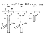
Fig.8 is a drawing showing a method for closing a
piping member of the PDP according to this embodiment.
Fig.9 is a drawing showing first variation of the
method and procedure for closing the piping member of the
PDP according to this embodiment.
Fig.10 is a drawing showing a second variation of the
method and procedure for closing the piping member of the
PDP according to this embodiment.
Fig.11 is a drawing showing a third variation of the
method and procedure for closing the piping member of the
PDP according to this embodiment.
Fig.12 is a plan view showing a bonding member for
the PDP according to this embodiment.
Fig.13 is a schematic sectional view for the
explanation of particle size of the bonding member.
Fig.14 is a plan view of a variation related to a method
of applying the bonding member.
Fig.15 is a plan view of another example related to
the method of applying the bonding member.
Fig.16 is a plan view of another example related to
the configuration of ridge of a division wall.
Fig.17 is a schematic view showing a method of sealing
the PDP according to this embodiment.
Fig.18 is a sectional view showing a method of
pressurizing during sealing.
Fig.19 is a sectional view showing a variation of the
method of pressurizing during sealing.
Fig.20 is a perspective sectional view of a portion
of the plasma display panel of the prior art.
Fig.21 is a perspective cutaway view schematically
showing configuration of a key portion of the PDP of the
prior art.
Fig.22 (a) through (c) are diagrams showing a
procedure of closing the piping member of the PDP according
to the prior art.
DESCRIPTION OF REFERENCE NUMERALS
- 1:
- Display electrode
- 2, 6:
- Dielectric film
- 3:
- Protective film
- 4:
- Upper panel substrate (Front substrate)
- 5:
- Address electrode
- 7:
- Division wall
- 8:
- Lower panel substrate (Back substrate)
- 10:
- Casing
- 11:
- Fluorescent substance
- 12:
- Compartment
- 13:
- Piping member
- 15:
- Bonding member
- 19:
- Sealing member
PREFERRED EMBODIMENTS OF THE INVENTION
Now preferred embodiments of the gas discharge panel
and the method for manufacturing the same according to the
present invention will be described below with reference
to the accompanying drawings.
Embodiment 1
Fig.1 is a schematic partial cutaway view of a plasma
display panel (PDP) that is an embodiment of the gas
discharge panel of the present invention. Reference will
be taken to this drawing in the description of the PDP
configuration according to this embodiment that follows.
This embodiment is basically the same as the
configuration of the PDP of the prior art described above
with reference to Fig.20, except for such points as a frit
glass 31 is used as a bonding member of the present invention.
Frit glass 31 will be described later.
In Fig.1, reference numeral 21 denotes a front panel
glass and 22 denotes a back panel glass. The front panel
glass 21 has display electrodes 24 patterned thereon, with
a dielectric film 28 and a protective film 29 being stacked
thereon, thereby forming a front substrate 104.
The back substrate 108 comprises the back panel glass
22, address electrodes 23 patterned thereon, division walls
30 and a fluorescent substance 25. The division walls 30
are formed integrally with dielectric films that cover the
address electrodes 23, and are formed by thermal spray of
alumina in this embodiment. This embodiment is different
from the configuration of Fig.20 also in that the division
walls 30 are formed integrally with dielectric films as
described above. The division walls 30 comprise a plurality
of plate-shaped ribs.
A PDP 100 is made in such a configuration as the front
substrate 104 and the back substrate 108 are disposed to
oppose each other, with the peripheries thereof being sealed
with a sealing member (not shown) made of glass having a
low melting point for forming a gas discharge space, while
the sealed losed space is filled with a rare gas (mixture
of helium gas and xenon gas) with a pressure exceeding 1 x 10⁵ Pa (760 Torr).
The division walls 30 are means for dividing
the gas discharge space into compartments 112 which act as
light emitting regions.
Now the frit glass 31 that characterizes the present
invention will be described below.
The frit glass 31 is applied onto the ridges of the
division walls 30 in advance in the manufacturing process.
Then with the front substrate 104 and the back substrate
108 being disposed to oppose each other and the panel being
sealed, the inner surface of the front substrate 104 and
the ridges of the division walls 30 are bonded together with
the molten frit glass 31.
The division walls 30 have some small holes on the
surface thereof. These holes occur when the division walls
30 are formed by thermal spraying. Since the molten frit
glass 31 penetrates the holes in the division walls 30,
strength of the division walls 30 increases and bonding
strength of the two substrates 104, 108 increases.
The division walls 30 and the dielectric film formed
integrally with the division walls 30 can be made by printing
or other method. The division walls'30 and the dielectric
film that lies below thereof may be made of the same material
or different materials.
Thus good picture quality with less cross talk or
image disturbance can be achieved.
With this configuration, it is possible to
increase the filling gas pressure to the atmospheric
pressure or higher, thereby achieving a PDP of high
brightness and high efficiency.
Embodiment 2
Fig.2 is a schematic partial sectional view of a PDP
according to second embodiment of the gas discharge panel
of the present invention. Configuration of the PDP according
to this embodiment will be described below with reference
to this drawing.
Configuration of the PDP according to this embodiment
is substantially the same as that shown in Fig.1, except
that bottom portions of the division walls 50 are bonded
onto the back substrate 108 by frit glass 52, and therefore
description thereof will be omitted.
The division walls 50 have the frit glass 31, 52
applied in advance to the bottom portions 50b and the ridges
50a thereof.
The frit glass 31 used for bonding the inner surface
of the front substrate 21 with the ridges 50a of the division
walls 50 may be either applied to the ridges 50a of the
division walls 50 or applied to the inner surface of the
front substrate 21 in a pattern before putting them together.
The frit glass 52 applied between the division walls
50 and the dielectric layer 53, on the other hand, is
effective in case the division walls 50 and the dielectric
layer 53 are made of different materials and are bonded
together with a relatively weak bonding force. As the frit
glass 52 infiltrates the holes formed in the division walls
50, it has an effect of reinforcing the division walls 50.
The frit glass 52 may be either formed at the same time as
the division walls 50 are formed, or formed in the specified
pattern on the dielectric layer 53 in advance before forming
the division walls 50 thereon.
Thus according to this embodiment, similar effects
as those of the first embodiment can be achieved.
Embodiment 3
Fig.3 (a) through (e) schematically show processes
of an embodiment of a method for manufacturing the gas
discharge panel according to the present invention. The
method for manufacturing the PDP according to this
embodiment will be described below with reference to these
drawings.
As shown in Fig.3(a), reference numeral 61 denotes
address electrodes and 62 denotes a back panel glass. In
this process, the address electrodes 61 are formed in a
pattern on the surface of the back panel glass 62.
Then as shown in Fig.3(b), a dielectric film 63 is
formed to cover the address electrodes 61 and the surface
of the back panel glass 62.
A resist 64 is then applied to the surface of the
dielectric film 63 and is patterned through exposure to light
as shown Fig.3(c).
Then as shown in Fig.3(d), portions missing the resist
64 are filled with division walls 65 made mainly of alumina
by thermal spraying, followed by filling with frit glass
66. The frit glass 66 may be applied either by thermal
spraying or other method, for example printing or simple
squeezing.
The resist 64 is then removed to leave the frit glass
66 on the ridges of the division walls 65 as shown in
Fig.3(e)
The back substrate made through the series of
processes described above is disposed to oppose the front
substrate and fired, with these substrates being sealed to
form a space which is then filled with a gas.
With the method described above, the PDP of a
configuration similar to those described in conjunction
with the first and the second embodiments is made very easily
wherein the front substrate and the back substrate are joined
together on the ridges of the division walls 65.
Use of this method eliminates the need for the process
of firing the division walls, thereby reducing the energy
consumption.
The firing processes can be combined into a single
process by applying a fluorescent substance to the surface
between the ribs of the division walls 65 after the division
walls have been formed by thermal spraying and the frit glass
has been applied, then firing the fluorescent substance and
carrying out boding and sealing of the two substrates at
the same time.
That is, in contrast to the prior art where the
division wall firing process, the fluorescent substance
firing process and the firing process carried out when
sealing the entire panel are carried out separately, two
firing processes are eliminated in this embodiment thereby
achieving great effects of reducing the facilities and
reducing the energy consumption.
Although a firing process is required when the
material to make the division walls includes fusible glass,
carrying out this firing operation and the firing operation
for sealing the entire panel simultaneously makes it
possible to eliminate two of the firing processes of the
prior art, similarly to the case described above.
Also in case the bonding member used for bonding the
ridge of the division walls and the inner surface of the
front substrate includes fusible glass, an organic binder
and an organic solvent, it is necessary to heat the bonding
member in a preliminary firing process in order to remove
the organic binder and the organic solvent included therein.
The preliminary firing process is provided after the
application of the bonding member and before sealing of the
panel.
Embodiment 4
Fig.4 (a) through (e) are diagrams schematically
showing processes according to one embodiment of a method
for manufacturing the gas discharge panel of the present
invention. The method for manufacturing the PDP according
to this embodiment will be described below with reference
to these drawings.
As shown in Fig.4(a), reference numeral 71 denotes
address electrodes, 72 denotes a dielectric film and 73
denotes back panel glass. A layer of a mixture of alumina
and frit glass (denoted by reference numeral 701 in the
drawing) is formed over the dielectric film 72, for the
formation of division walls 74.
Then a layer of frit glass 75 is formed over the surface
as shown in Fig.4(b). The division walls 74 and the frit
glass 75 are formed by thermal spraying.
The frit glass 75 may also be formed by applying the
glass by a printing process and then firing.
Then as shown in Fig.(c), a pattern is formed by
exposure of a resist 76, a dry film or the like to light.
The material is then removed by sand blast from
portions where the resist 76 is not deposited thereby to
form the division walls 74, as shown in Fig.4(d). The
division walls 74 have the frit glass film described in
conjunction with Fig.4(b) deposited on the ridges thereof.
The front substrate and the back substrate are then
sealed to assemble the panel by using the sealing member
as shown in Fig.4(e), with the panel being sealed by firing
while bonding with the division walls 74 at the same time.
While the sealing operation and bonding of the ridges of
the division walls 74 with the inner surface of the front
substrate are preferably carried out simultaneously in view
of energy saving in the manufacturing process, they may also
be carried out in separate processes as a matter of course.
Although the fluorescent substance 78 is applied
after forming the division walls 74, the fluorescent
substance 78 may be fired either during sealing or separately
before sealing.
Number of firing processes can be reduced also with
this manufacturing method that provides great effects of
reducing the manufacturing facilities and energy
consumption.
Also according to this embodiment, since the mixture
of alumina and frit glass is used as the material to make
the division walls and the frit glass fills the voids of
alumina during sealing, void ratio decreases and division
walls with less outgassing can be achieved. As a consequence,
it is made possible to decrease pollution due to impurity
gas and elongate the service life of the panel.
Embodiment 5
Fig.5 schematically shows a method forming the
division walls by thermal spraying, which is an embodiment
of a method for manufacturing the gas discharge panel
according to the present invention. The thermal spray method
of this embodiment will be described below with reference
to this drawing.
As shown in Fig.5, reference numeral 81 denotes a
thermal spray torch and 82 denotes a coolant gas. The coolant
gas 82 removes unnecessary heat generated by the thermal
spray and keeps the substrate temperature within 200°C.
Reference numeral 83 denotes a powdery material to make the
division walls 84 that is supplied with frit glass 87.
Reference numeral 86 denotes a dry film for masking portions
where the division walls are not to be formed. Reference
numeral 85 denotes the back panel glass, 89 denotes the
address electrodes and 88 denotes the dielectric film.
The material to make the division walls included in
the molten powder 83 sprayed from the thermal spray torch
81 is deposited in gaps between the dry films 86 which have
been exposed to light and developed, to form a film having
thickness of about 60% of the gap depth, followed by spraying
of the frit glass 87 to form a film. Because the thermal
spray is applied while cooling with the coolant gas 82, the
dry film 86 is cooled down to such a temperature that is
not harmful. When the dry film is removed, the division walls
84 with the frit glass 87 layer formed thereon are obtained.
According to this embodiment, the division walls with
the frit glass layer formed on the ridges thereof can be
formed by a very simple method, and therefore number of the
firing processes can be reduced while providing great
effects of reducing the manufacturing facilities and energy
consumption.
According to this embodiment, as described above, the
front substrate and the back substrate are bonded together
and therefore the panel does not swell at the middle unlike
the prior art even when the inner pressure of the PDP
increases.
Also in the presence of vibration, there occurs no
such problem as the front substrate and the back substrate
vibrate independently of each other due to difference in
the resonance frequency arising from the difference in the
mass thereof.
As a consequence, better image quality with less cross
talk and less image disturbance can be achieved even in such
places as in an airplane where the atmospheric pressure is
unstable or low, and in an environment which is affected
by much vibrations.
Also such a configuration as described above allows
it to increase the filling gas pressure to the atmospheric
pressure or higher, thus making it possible to achieve the
PDP of high brightness and high efficiency.
In addition, the manufacturing method of the present
invention makes it possible to greatly reduce the number
of the firing processes and provide great effects of reducing
the manufacturing facilities and energy consumption.
As will be apparent from the above description of the
preferred embodiments, the PDP of the present invention has
such a configuration as the division walls formed on the
back substrate or on the front substrate are bonded to the
other substrate by means of the frit glass. And the
manufacturing method is such that the division walls are
formed by thermal spraying with the frit glass also being
applied to the ridges thereof by thermal spraying, while
bonding of the division walls and the front substrate,
sealing of the back substrate and the front substrate and
firing of the fluorescent substance are carried out
simultaneously.
As a consequence, because the front substrate and the
back substrate are bonded with the frit glass on the ridges
of the division walls, the panel does not break nor swell
even when the pressure of the gas that fills the inside the
panel is higher than the atmospheric pressure. Thus the
problems including cross talk do not occur, while good image
is obtained and higher safety is achieved even when used
onboard an airplane or the like. Also even when the panel
is subject to vibration or the like, the substrates do not
deflect because the front substrate and the back substrate
are bonded together, and therefore good image is obtained
even when used onboard a train, automobile or the like.
Furthermore, because the pressure of the discharge gas that
fills the inside can be made higher than the atmospheric
pressure according to this embodiment, PDP of high
brightness and high efficiency can be achieved.
Also according to the present invention, because
bonding of the division walls and the front substrate,
sealing of the back substrate and the front substrate and
firing of the fluorescent substance are carried out
simultaneously unlike the prior art, it is made possible
to reduce the number of the firing processes and reduce the
electric energy required for manufacturing the PDP, thus
achieving cost reduction.
Now preferred embodiment of the gas discharge panel
and the method for manufacturing the same according to the
present invention will be described below with reference
to the accompanying drawings.
Embodiment 6
Fig.6 is a perspective cutaway view schematically
showing the configuration of a key portion of the PDP
according to one embodiment of the gas discharge panel of
the present invention. Fig.7 is a sectional view according
to a variation thereof. Fig.8 is a drawing showing a method
for closing the piping member in the manufacture of the PDP
according to this embodiment. Fig.9 through Fig.11 are
drawings showing first through third variations of the
method and procedure for closing the piping member.
As the overall configuration of the PDP according to
this embodiment is basically the same as that of the PDP
of the prior art described with reference to Fig.20 and
Fig.21 in many aspects, parts or portions identical or
equivalent to those described with reference to Fig.20 and
Fig.21 will be denoted with the same reference numerals.
As shown in Fig.6, the casing 10 according to this
embodiment has such a configuration as the upper panel
substrate 4 and the lower panel substrate 8 are disposed
to oppose each other while peripheries of the two panel
substrates 4, 8 are sealed with a sealing member 9 made of
glass having a low melting-point, thereby forming a
discharging space therein.
The upper panel substrate 4 is a substrate made of
glass having a plurality of display electrodes 1, the
dielectric layer 2 made of glass having a low melting point
covering the display electrodes 1 and a protective film 3
made of magnesium oxide in a thin film being formed on the
inner surface thereof. The lower panel substrate 8 is a
substrate made of glass having a plurality of data electrodes
5 disposed at right angles to the display electrodes 1 and
a dielectric layer 6 made of glass having a low melting point
being formed on the inner surface thereof, while division
walls 7 made of glass having a low melting point are formed
in parallel to each other at predetermined positions on the
dielectric layer 6 in order to separate compartments of light
emitting regions.
The division walls 7 have, on the ridges thereof,
bonding members 15 made of a material having a low melting
point such as frit glass (melting point of about 450°C) or
water glass having a melting point lower than that of the
material making the division wall 7 which is from 500 to
600°C. The division walls 7 formed on the lower panel
substrate 8 and the upper panel substrate 4 are bonded by
the bonding member 15.
The bonding member 15 may also be made of an
ultraviolet adhesive having low hygroscopicity and less
outgassing or a common sealing material used in vacuum
applications. Although the bonding member 15 is made of a
material having a melting point lower than that of the
division walls 7 in this embodiment in consideration of the
convenience in the manufacturing process, a common adhesive
may also be used regardless of the melting point as long
as the manufacturing process allows it. Also the bonding
members 15 may not necessarily be provided along the entire
length of the ribs of the division walls 7. That is, the
bonding members 15 may be provided at separate predetermined
positions, as a matter of course.
Meanwhile, as shown in Fig.7, the bonded portions 2a
on the dielectric layer 2 of the upper panel substrate 4,
namely the portions to be bonded with the ridges of the
division walls 7 by means of the bonding members 15, and/or
portions 6a of the dielectric layer 6 of the lower panel
substrate 8 where the division walls 7 are to be formed,
namely either one or both of the predetermined portions 2a,
6a of the dielectric layer 2 and the dielectric layer 6 may
have rough surface with fine irregularities formed thereon.
With this configuration, the rough surface provides an
anchoring effect.
Specifically, bonding strength between the
dielectric layer 2 of the upper panel substrate 4 and the
ridges of the division walls 7 via the thin protective film
3 and the bonding member 15 and the bonding strength between
the dielectric layer 6 of the lower panel substrate 8 and
the bottom of the division walls 7 are increased.
The rough surface may be provided by such a common
method as masking the portions which are not to be roughened
and applying sand blast. In this case, because the dielectric
layer 6 of the lower panel substrate 8 is covered by the
fluorescent substance 11, the dielectric layer 6 may also
be roughened over the entire surface thereof.
In addition, the dielectric layer 6 in each light
emitting region separated by the division walls 7 is coated
with the fluorescent substance 11 in order to produce color
display. The inner space of the casing 10 formed by bonding
the upper panel substrate 4 and the division walls 7 of the
lower panel substrate 8 via the bonding members 15 is filled
with a discharge gas comprising a mixture of helium, xenon,
neon or the like, with an inner pressure exceeding 1 x 10⁵ Pa (760 Torr),
for example from 1 x 10⁵ Pa to 1.33 x 10⁵ Pa (750 Torr to 1000 Torr).
As shown in Fig.6, the lower panel substrate 8 bears
the piping member 13, that was used when purging air from
the inner space of the casing 10 and filling it with the
discharge gas, remaining thereon as bonded by using the same
material as the sealing member 9.
With this configuration, even when the inner pressure
of the casing 10 is higher than the pressure acting on the
outer surface of the casing 10, namely atmospheric pressure,
the upper panel substrate 4 and the lower panel substrate
8 are bonded together by the bonding members 15 provided
on the ridges of the division walls 7. As a result, the
adjoining compartments 12 that serve as the light emitting
regions do not communicate with each other through gaps,
that is, the adjoining compartments 12 are surely isolated
from each other, and such a problem does not occur as the
panel substrates 4, 8 swell toward the outside and deform.
PDPs may be used onboard airplanes or trains, and
subject to changes in the atmospheric pressure during sharp
ascent or sharp dive of an airplane or vibration of a running
train. Even in such cases, provided that the upper panel
substrate 4 and the lower panel substrate 8 that constitute
the casing 10 are bonded together by the bonding members
15 provided on the ridges of the division walls 7, such a
problem never occurs as the casing 10 swells toward the
outside and deform when the atmospheric pressure changes
or under the presence of vibration.
Now the method for manufacturing the PDP of the
configuration described above according to the preferred
embodiment of the gas discharge panel of the present
invention will be described below with reference to the
accompanying drawings.
First, the upper panel substrate 4 whereon the display
electrodes 1, the dielectric layer 2 and the protective layer
3 are formed, and the lower panel substrate 8 whereon the
data electrodes 5, the dielectric layer 6 and the division
walls 7 are formed and the fluorescent substance 11 applied
thereon are manufactured.
With these panel substrates being prepared, the
bonding members 15 made of a material having a low melting
point such as frit glass is applied onto the ridges of the
division walls 7 of the lower panel substrate 8.
While the bonding members 15 are applied by such a
technique as screen printing or transferring by means of
a stamper, the bonding members 15 may also be provided by
lift-off or the like before applying the fluorescent
substance 11 thereon. Also in case the division walls 7 are
formed through a plurality of screen printing operations,
the bonding members 15 can be provided by forming only the
uppermost layer from frit glass or the like, or alternatively,
the frit glass or the like that makes the bonding members
15 may be applied to predetermined portions of the upper
panel substrate 4 which correspond to the division walls
7 provided on the lower panel substrate 8. In screen printing,
it is common to form a pattern through which an adhesive
material of predetermined viscosity passes for a screen
plate that makes contact with the ridges of the division
walls 7, the bonding members 15 may also be provided only
on the ridges of the division walls 7 by screen printing,
after making the screen plate through the entire surface
of which the adhesive material can pass.
Then the upper panel substrate 4 and the lower panel
substrate 8 are disposed to oppose each other via the
division walls 7 whereon the bonding members 15 are provided
as described above, and the two panel substrates 4, 8 are
heated with the sealing member 9 provided between the
peripheries thereof. This causes the upper panel substrate
4 and the lower panel substrate 8 to be sealed on the
peripheries thereof by the sealing member 9, resulting in
the formation of the casing 10. At this time, the upper panel
substrate 4 and the lower panel substrate 8 are bonded
together by the bonding members 15 that has melted in the
heating process.
The piping member 13 that communicates with the inside
of the casing 10 via the through hole 8a formed in the lower
panel substrate 8 that constitutes the casing 10 is attached
at a place outside the lower panel substrate 8.
And through the piping member 13, the inside the
casing 10 is evacuated of the air and is filled with the
discharge gas.
Then the piping member 13 is closed thereby to seal
the inner space of the casing 10, thus completing the PDP
shown in Fig.6.
In case the casing 10 is filled with the discharge
gas with a pressure exceeding 1 x 10⁵ Pa (760 Torr), the piping member
13 is closed by a method, for example, shown in Fig.8.
First, as shown in Fig.8, the piping member 13 that
communicates with the inside of the casing 10 via the through
hole 8a formed on the lower panel substrate 8 that
constitutes the casing 10 is attached at a place outside
the lower panel substrate 8. The casing 10 with the piping
member 13 attached thereto is placed at a proper position
in a pressured chamber 16, while heating means 17 such as
an induction heater or an electric heater is disposed along
the periphery of the closing portion 13a of the piping member
13.
Through the piping member 13, air inside the casing
10 is purged and the inside of the casing 10 is filled with
the discharge gas with a predetermined pressure exceeding
1 x 10⁵ Pa (760 Torr).
Then the inner pressure of the pressured chamber 16
is set to a level higher than the pressure of the discharge
gas in the casing 10.
As this makes the inner pressure of the pressured
chamber 16 higher than the inner pressure of the casing 10,
the piping member 13 can be closed in a procedure similar
to that of the prior art.
That is, the closing portion 13a of the piping member
13 is heated and melted by the heating means 17. As the lower
portion of the closing portion 13a is pulled away from the
casing 10, the closing portion 13a of the piping member 13
which has been cut off by melting is closed, thereby sealing
the casing 10. While the piping member 13 is closed by setting
the pressure acting on the outer surface of the casing 10
higher than the inner pressure of the discharge gas in this
embodiment, it is not necessary to employ such a laborious
method. It is a matter of course that the piping member 13
can be closed similarly to the prior art simply by setting
the pressure acting on the piping member 13 higher than the
discharge gas pressure that fills the casing 10.
Now variations of the method and procedure of closing
the piping member 13 will be described below with reference
to Fig.9 through Fig.11.
Fig.9(a) through Fig.9(c) show the first variation
of the method and procedure of closing the piping member
13.
This method uses a sealing jig 17 that has a projection
17a having a section of semicircular or triangular
configuration formed thereon to press the piping member 13
along the radial direction from at least two directions
opposing along the radial direction of the piping member
13, and has a function of heating the piping member 13 via
the projection 17a. With this method, the piping member 13
that communicates with the inside of the casing 10 via the
through hole 8a formed in the lower panel substrate 8 that
is one of the panel substrates is attached and, after purging
the air from the inside of the casing 10 and filling it with
the discharge gas through the piping member 13, the
projection 17a of the sealing jig 17 is pressed against the
closing portion 13a of the piping member 13 as shown in
Fig. 9(a). Then the piping member 13 is heated while pressing
the projection 17a of the sealing jig 17 thereto along the
radial direction thereof as shown in Fig.9(b), thereby
cutting off the piping member 13 by melting it with the heat
as shown in Fig.9(c). When this method is employed, the
closing portion 13a is closed as a result of pressing the
projection 17a against the piping member 13 which has been
heated to melt, and therefore the piping member 13 can be
easily closed thereby to seal the casing 10, despite the
inner pressure of the casing 10 being higher than the
atmospheric pressure.
The piping member 13 may also be closed as in the second
variation shown in Fig.10, where a heating jig 18 fitted
on the piping member 13 from the outside thereof is heated
by means of a gas burner 14 or the like to melt the closing
portion 13a of the piping member 13, while forcing the lower
portion of the closing portion 13a in the direction of arrow,
thereby to twist off the closing portion 13a while forcing
it toward the casing 10. The heating jig 18 may be anything
that can prevent the piping member 13 from swelling toward
the outside due to the inner pressure that is higher than
the atmospheric pressure and, while being omitted in the
drawing, may be made of a metallic wire mesh. In case the
heating jig 18 is stuck with the piping member 13, the heating
jig 18 is left stuck with the piping member 13 which causes
no problem at all.
Furthermore, the method of closing the piping member
13 described above may be replaced by the method shown in
Fig.11(a) and Fig.11(b).
With this method of the third variation, the piping
member 13 that communicates with the inside of the casing
10 via the through hole 8a formed in the lower panel substrate
8 that is one of the panel substrates is attached and, after
purging the air from the inside of the casing 10 and filling
it with the discharge gas through the piping member 13, the
gas burner 14 or the like is used from the outside to heat
and melt the sealing member 19 that has been formed in a
short rod from a material having a melting point lower than
that of the piping member 13 and housed in the piping member
13, thereby closing the piping member 13 as shown in
Fig.11(b). Then unnecessary portion of the piping member
13 closed with the sealing member 19 is removed by cutting
off or other method. The sealing member 19 may be either
housed in the piping member 13 in advance, put into the piping
member 13 that has been attached to the lower panel substrate
8, or made of a material mixed with a black pigment to have
high heat absorbing characteristic and is melted by
irradiation of laser light.
In case the casing 10 is filled with the discharge
gas with a pressure not higher than 0.66 x 10⁵ Pa (500 Torr), it is common
to employ the manufacturing method comprising processes
similar to those of the prior art. But the method of this
embodiment may also be employed even in such a case where
the inner pressure of the casing 10 is lower than the external
pressure. This is known not claimed as an embodiment of the present invention.
As will be clear from the foregoing description, the
gas discharge panel according to the present invention is
characterized by, for example, the panel substrates that
constitute the casing that are bonded together via the
bonding members provided on the ridges of the division walls,
while the casing 10 is filled with the discharge gas
of a pressure exceeding 1 x 10⁵ Pa (760 Torr). The bonding member is
preferably made of a material having a melting point lower
than that of the division wall. In case the casing of such
a configuration that the panel substrates are bonded
together is used, the casing never deforms by swelling toward
outside. In case the casing 10 is filled with the discharge
gas with a pressure exceeding 1 x 10⁵ Pa (760 Torr), there is such an
advantage that brightness of the gas discharge panel is
improved. The improvement in the brightness of the gas
discharge panel is due to the improved gas discharge
efficiency.
The method for manufacturing the gas discharge panel
according to the present invention is for such a case, for
example, as the inner pressure of the casing is higher than
the external pressure during manufacturing, and is
characterized in that the piping member is closed while
keeping the pressure acting on at least the piping member
from the outside higher than the discharge gas pressure that
fills the casing, or the piping member is closed by heating
while pressing the piping member from at least two directions
opposing along the radial direction of the piping member,
or the piping member is closed by melting the sealing member
housed in the piping member. According to these
manufacturing methods, the piping member can be easily and
surely closed even when the inner pressure of the casing
is higher than the external pressure.
As described above, according to the gas discharge
panel of the present invention, due to such a configuration
as, for example, the panel substrates that constitute the
casing are bonded together via the bonding members provided
on the ridges of the division walls, such problems never
occur as a gap is produced between the division walls and
the panel substrate or the casing deforms by swelling toward
the outside. Thus there occurs no problem even when the
casing is filled with the discharge gas with a pressure
exceeding 1 x 10⁵ Pa (760 Torr), thus making it possible to improve the
brightness of the gas discharge panel.
Also according to the method for manufacturing the
gas discharge panel of the present invention, even when the
inner pressure of the discharge gas filling the casing is
higher than the atmospheric pressure, the
piping member can be easily and surely closed and therefore
the gas discharge panel of improved brightness can be easily
manufactured.
According to the embodiments described above, the
bonding members 15 can be formed on the ridges of the division
walls 7 by, for example, screen printing or the like. However,
the ridges of the division walls 7 are very narrow and long
and it may be difficult to form the bonding members 15
uniformly thereon.
Also while the division walls 7 can be formed by
printing, lift-off, sand blast or other process, the ridges
may have uneven surfaces. The bonding member may not be
formed on recessed portions on the ridges of the division
walls 7, in which case the upper panel substrate 4 and the
division wall 7 are not bonded together at the recessed
portions, which may lead to deteriorated display quality
at such portions.
Also when an excessive amount of the bonding member
15 is formed or the bonding member 15 is formed beyond the
width of the division wall 7, the bonding member 15 after
bonding has a width larger than the width of the division
wall 7, where the light emitting region as viewed from the
outside of the upper panel substrate 4 becomes narrower
thereby leading to a decrease in brightness.
Meanwhile the sealing member 9 of the prior art is
formed only on the periphery of the panel substrate, and
pressure is applied only to the periphery of the panel
substrate when sealing. However, while the division walls
7 and the upper panel substrate 4 must be bonded surely by
the bonding members 15 in order to make the casing that does
not deform, reliable bonding may not be achieved in the
display region inside the panel substrate by applying
pressure only to the periphery of the panel substrate even
with such a configuration.
In consideration of these problems, a gas discharge
panel and a method for manufacturing the same that are
capable of preventing the PDP from deforming more reliably
and achieve improvement in brightness will be described
below.
Fig.12 is a plan view showing the application of the
bonding members 15, and Fig.14 is a plan view of a variation
thereof. Fig.13 is a schematic sectional view for the
explanation of the relationship between particle size of
the bonding member and the division wall width of the PDP
according to this embodiment. Fig.17 is a sectional view
showing a method of applying pressure during sealing. Fig. 18
and Fig.19 are sectional views showing the method of
pressurizing during sealing.
Overall configuration of the PDP according to this
embodiment is basically the same as that shown in Fig.6,
and therefore parts or portions identical or equivalent to
those described with reference to Fig.6 will be denoted with
the same reference numerals, and description thereof will
be omitted.
The PDP according to this embodiment is as described
with reference to Fig.6.
That is, the ridges of the division walls 7 bear the
bonding members 15 made of a transparent material formed
thereon linearly along the longitudinal direction of the
division walls 7 as shown in Fig.12. The division walls 7
formed on the lower panel substrate 8 and the upper panel
substrate 4 are bonded to each other via the bonding members
15.
The bonding members 15 formed on the ridges of the
division walls 7 may partially project beyond the division
wall width due to unevenness in the amount of application
or the like, as described previously. Also when an excessive
amount is applied when bonding with the upper panel substrate
4, the bonding member may be spread on top of the division
wall and intrude into the light emitting region beyond the
width of the division wall.
However, since the bonding member 15 is made of a
transparent material, a little amount of it intruding into
the light emitting region does not block the emitted light
and does not cause deterioration in the display quality,
particularly brightness.
In addition, the dielectric layer 6 in each light
emitting region separated by the division walls 7 is coated
with the fluorescent substance 11 to produce color display.
And the casing 10 comprising the upper panel substrate 4
and the division walls 7 provided on the lower panel
substrate 8 bonded together via the bonding members 15
is filled with the discharge gas comprising a mixture of
helium, xenon and neon at a pressure exceeding 1 x 10⁵ Pa (760 Torr),
for example from 1 x 10⁵ Pa to 1,33 x 10⁵ Pa (760 Torr to 1000 Torr).
Now a variation of the bonding members 15 will be
described below with reference to Fig.13.
The frit glass which has been commonly used for the
bonding member includes a material such as lead oxide and
a filler such as ceramics added to control the thermal
characteristics and to obtain desired bonding strength with
the glass substrate.
Fig.13 shows a case where maximum particle size D of
the material such as the filler included in the bonding
members 15 does not exceed the width W of the division walls
7. In this case the bonding member 15 does not project beyond
the width of the division wall when the largest particle
is located at the center of the division wall 7. Even when
the largest particle is formed at a position somewhat offset
from the center of the division wall 7, it does not
significantly come out of the width of the division wall.
Thus the PDP having good display characteristic can be
obtained without covering the display region with the
bonding members 15 after bonding the division walls 7 and
the upper panel 4. What is important here is to keep the
bonding members from significantly coming out of the width
of the division wall after bonding, and this can be achieved
with the configuration described above. To keep the bonding
members from significantly coming out of the width of the
division wall means to keep the bonding member from having
such a width that substantially decreases the fluorescent
substance region of each compartment 12 (Fig.6). The
fluorescent substance region is determined by the area of
the compartment 12 where the fluorescent substance 11 is
applied.
In case there is a gap larger than 5µm between the
division walls and the upper panel substrate, wile not shown
in the drawing, cross talk or other deterioration in display
occurs when turning on the panel.
When the particles included in the bonding member are
large in size, on the other hand, the bonding member tends
to be formed unevenly, there is a possibility that the
division walls and the upper panel are bonded to each other
only at a portion where the largest particle lies. For this
reason, it is desirable that the maximum particle size
included in the bonding member be 5 µm or less. In this
embodiment, width W of the rib of the division wall (Fig.13)
is about 40µm.
A PDP according to another variation of the bonding
members 15 will be described below with reference to Fig. 14.
While the bonding members 15 described above are
provided on the ridges of the division walls 7, the bonding
members 15 are provided in linear configuration on the inner
surface of the panel substrate 4. That is, as shown in Fig. 14,
the bonding members 15 are formed linearly at the center
between one set of display electrodes and an adjoining set
of display electrodes which are disposed in a pair, in such
a direction that crosses the division walls 7 formed on the
lower panel substrate 8 substantially at right angles (for
example substantially at right angles to the longitudinal
direction of the division walls 7).
In this case, the bonding members 15 may be formed
either by screen printing or drawing with a dispenser or
the like. The two panel substrates 4, 8 that oppose each
other are bonded together at points where the bonding members
15 and the division walls cross. Since the bonding members
15 are formed on a plane, they can be formed easily, and
alignment can also be easily done when sealing because both
the division walls 7 and the sealing member 15 have linear
configuration and cross each other. Bonding is also made
more reliably.
The bonding members 15 also have a function of
visually separating pixels which adjoin each other in the
longitudinal direction of the division walls 7, prevent the
casing 10 from swelling toward outside and deforming, and
have an effect of improving the contrast.
Although this embodiment is a case where the bonding
members 15 are formed on the inner surface of the upper panel
substrate 4, the bonding members 15 may also be formed on
the ridges of the division walls 7 formed on the lower panel
substrate 8 without any problem, while proving more
effective in achieving more reliable bonding because
sufficient amount of the bonding member is formed in the
bonding area.
Of course the contrast of the PDP can be improved
further by making the bonding members 15 shown in Fig.13
and Fig.14 of a light absorbing material.
A PDP according to another variation of the bonding
members 15 will be described below with reference to Fig.15.
While the bonding members 15 described above are provided
on most part of the ridges of the division walls 7 for bonding
with the upper panel substrate 4, bonding may not necessarily
be done on most part and partial bonding shown in Fig.15
is also effective.
The bonding has, as described repetitively above, in
addition to the apparent effect of preventing the panel from
swelling toward the outside and deforming, and effect of
preventing cross talk from occurring between discharge
cells by filing the gap between the ridges of the division
walls and the upper panel substrate with the bonding member
and completely separating the discharge cells.
While it can be freely determined where to bond or
not to bond, it is more preferable to provide the bonding
members 15 at and around the intersects of the ridges of
the division walls and the display electrode 1. It is because
larger discharge occurs at these points.
While Fig.15 shows a case of uniform bonding in the
vicinity of the display electrode 1, bonding may not
necessarily be uniform and may be provided only at portions
where cross talk is likely to occur or may be done linearly
on some part of the ridges of the division walls.
Now another embodiment will be described below with
reference to Fig.16. The PDP according to this embodiment
has, similarly to the prior art, the casing of such a
configuration as the upper panel substrate 4 with a plurality
of display electrodes 1 formed thereon and the lower panel
substrate 8 with a plurality of data electrodes 5 and the
division walls formed on the inner surface thereof in a
direction at right angles to the display electrodes 1 are
disposed to oppose each other, and the peripheries of the
panels are sealed by the bonding member 15 made of glass
having a low melting point. The division walls 7 have grooves
on the ridges thereof, while the grooves are filled with
the bonding members 15 thereby to bond the upper panel
substrate 4 and the division walls 7 via the bonding members
15. The division walls 7 are formed as follows. A resin coat
layer is formed by laminating a dry resist film on the lower
panel substrate 8 and, after selective exposure by using
an exposure mask, a negative pattern is made by development
process. An opening of the pattern is filled with a paste
by squeezing or the like to the same height as the surface
of the resin coat layer. Then the lower panel substrate 8
is dried to remove the solvent included in the paste, upon
which the paste is recessed at the middle. This recessed
shape can be adjusted by controlling the amount of the
solvent included in the paste, the amount of the filler or
the opening configuration of the resin coat layer.
Alternatively, the recessed shape can be made by machining
the ridges of the division walls 7 by mechanical means,
irradiating with laser light or the like. When the recesses
on the division walls 7 formed as described above is filled
with the bonding members 15, bonding area between the
division walls 7 and the bonding members 15 increases leading
to increased bonding strength and also increases the
apparent area of light emitting due to decreased projection
of the bonding members 15 beyond the width of the division
walls.
Now a method for manufacturing the PDP according to
this embodiment will be described below following the order
of procedure.
First, the upper panel substrate 4 with the display
electrodes 1, the dielectric layer 2 and the protective layer
3 formed thereon and the lower panel substrate 8 with the
data electrodes 5, the dielectric layer 6 and the division
walls 7 formed and the fluorescent substance 11 applied
thereon are prepared, and the bonding member 15 made of a
material having a low melting point such as frit glass are
provided on the ridges of the division walls 7.
While screen printing or transfer by means of a
stamper is employed for providing the bonding members 15,
they can also be applied by lift-off or the like. Or,
alternatively, the bonding members 15 may also be provided
by forming frit glass layers on the ridges of the division
walls 7. Such a method may also be employed as frit glass
that would become the bonding members 15 is applied to
predetermined portions of the upper panel substrate 4 that
correspond to the division walls 7 provided on the lower
panel substrate 8.
In screen printing, it is common to form in advance
a pattern through which an adhesive material of
predetermined viscosity passes for the screen that makes
contact with the ridges of the division walls 7. However,
the bonding members 15 may also be provided only on the ridges
of the division walls 7 by screen printing, after making
a screen through the entire surface of which the adhesive
material can pass.
Then the upper panel substrate 4 and the lower panel
substrate 8 are disposed to oppose each other via the
division walls 7 having the bonding members formed thereon
as described above, and the sealing member 9 is interposed
between the peripheries of the two panel substrates 4, 8.
In this case, when the panel substrates are heated
while applying pressure from the outer surface toward the
inner surface, as shown in Fig.17, the upper panel substrate
4 and the lower panel substrate 8 are sealed on the
peripheries thereof by the sealing member 9. At the same
time, the upper panel substrate 4 and the lower panel
substrate 8 are bonded to each other by the bonding members
15 which have been melted by the heat in the display area
at the center, thereby forming the casing 10.
Further, the lower panel substrate 8 is fitted on an
external position thereof with the piping member 13 that
communicates with the casing 10 via the through hole 8a
formed on the lower panel substrate 8 that constitutes the
casing 10. Then after purging the air from the inside of
the casing 10 and filling the inner space with the discharge
gas the piping member 13, the piping member 13 is closed
thereby sealing the inner space of the casing 10, thus
completing the PDP shown in Fig.6.
Pressurization when bonding the upper panel substrate
4 and the lower panel substrate 8 is carried out, for example,
by the method shown in Fig.18.
First, the upper panel substrate 4 and the lower panel
substrate 8 that constitute the casing 10 are tentatively
secured at predetermined positional relationship and placed
on a flat base 16.
Then a plurality of pressurizing jigs 23 are placed
at predetermined positions. The pressurizing jig 23
comprises a spring receiver A (20), a spring receiver B (22),
a spring 21 and a bolt 19, while the spring receiver A (20)
and the spring receiver B (22) are separated with the spring
21 interposed therebetween.
Pressurizing force of the spring 21 can be controlled
by adjusting the position of the spring receiver B (22) by
means of the bolt 19. The pressurizing jig 23 is inserted
between the casing 10 and a frame 18 that is secured on the
base 16 via supports 17, while adjusting the position of
the spring receiver B (22) by means of the bolt 19 so that
the total length of the pressurizing jig 23 becomes greater
than the distance. Since the spring 21 is installed while
being compressed, pressure is applied to the two panel
substrates.
Frit glass that makes the bonding members 15 and the
sealing member 9 is normally used while being heated to 450°C
and melted, and the spring 21 used herein is of course made
of a material that does not lose resilience at 450°C. For
example, Inconel is used.
Now a variation of the method of pressurization will
be described below with reference to Fig.19.
First, it is the same as the embodiment described
above that the upper panel substrate 4 and the lower panel
substrate 8 that constitute the casing 10 are tentatively
secured in predetermined positional relationship and placed
on the flat base 16. Then a shock absorber 24 made of a
resilient material that does not change the characteristics
thereof when heated to 450°C is placed to cover the entire
of the casing 10. For the shock absorber 24, steel
wool or the like can be used.
Then a plate 25 having a predetermined weight, uniform
thickness and a size that covers the entire surface of the
casing is placed on the shock absorber 24 that is placed
on the casing 10. It is necessary to interposed the shock
absorber 24 between the plate 25 and the casing 10, because
a foreign matter interposed therebetween may generate
uneven gap between the upper panel substrate 4 and the lower
panel substrate 8 that constitute the casing 10 due to
partially changed pressure and, in case the foreign matter
is large, localized force may be applied eventually leading
to breakage of the casing 10.
As described above, the gas discharge panel according
to the present invention has such an advantage that, because
the upper panel substrate and the lower panel substrate that
constitute the casing are bonded to each other via the
bonding members, problems of gap being generated between
the division walls and the panel substrate and the casing
swelling toward the outside to deform never occur, even when
the casing is filled with the discharge gas with a pressure
exceeding 0,66 x 10⁵ Pa (500 torr). According to the invention, the casing is filled with
the discharge gas with a pressure exceeding even 1 x 10⁵ Pa
(760 Torr).
In addition, deterioration in the characteristics of
the panel does not occur since the bonding member does not
come out of the width of the division walls or, should it
come out, it is made of a transparent material. Also forming
the bonding members in a direction at right angles to the
division walls has an effect of separating the pixels that
adjoin each other in the direction of the division walls,
thereby improving the contrast.
The method for manufacturing the gas discharge panel
according to the present invention has such an advantage
that the division walls and the opposing panel substrate
can be bonded uniformly over the entire area of the casing,
and therefore the gas discharge panel of improved brightness
can be easily manufactured.
While the PDP in the embodiments described above has
the dielectric film, the invention is not limited to this
configuration and a configuration without dielectric film
may also be employed.
While the gas discharge panel in the embodiments
described above is PDP of AC type, the gas discharge panel
is not limited to PDP of AC type and the present invention
may also be applied to PDP of DC type, as a matter of course.
The first panel substrate and the second panel
substrate of the present invention correspond respectively
to the front panel substrate and the back panel substrate
in the embodiments described above. However, the present
invention is not limited to this arrangement and may be
embodied in such an arrangement as the first panel substrate
corresponds to the back panel substrate and the second panel
substrate corresponds to the front panel substrate. In this
case, bases of the division walls rest on the inner surface
of the front panel substrate and ridges of the division walls
rest on the inner surface of the back panel substrate.
A variation of the example shown in Fig.8 and Fig.9 is a
method for manufacturing the gas discharge panel comprising
the first panel substrate having the first electrode, the
second panel substrate having the second electrode opposing
the first panel substrate, the sealing portion provided
between the peripheries of the two substrates for forming
the gas discharge space between the first and second panel
substrates and division walls provided on the second panel
substrate to divide the gas discharge space, wherein the
manufacturing method comprises an assembly process of
assembling the first panel substrate and the second panel
substrate into the gas discharge panel by means of the
sealing portion, a process of attaching the piping member
that communicates with the gas discharge space via a through
hole formed in the first or the second panel substrate onto
the panel substrate that has the through hole, a sealing
process of filling the gas discharge space with the discharge
gas by using the piping member and a sealing process of
closing the piping member. This has an effect of being
capable of providing a manufacturing method different from
the prior art.
Industrial Utilization
As will be clear from the description give so far,
the present invention provides a gas discharge panel capable
of producing more stable image with less possibility of cross
talk than the prior art, and a method for manufacturing the
same.
The present invention also provides a method for
manufacturing the gas discharge panel that is capable of
reducing the number of firing processes over the prior art.
The present invention also provides a method for
manufacturing the gas discharge panel that is capable of
increasing the brightness over the prior art.