EP0945886B1 - Gaseous discharge panel and manufacturing method therefor - Google Patents
Gaseous discharge panel and manufacturing method therefor Download PDFInfo
- Publication number
- EP0945886B1 EP0945886B1 EP97947930A EP97947930A EP0945886B1 EP 0945886 B1 EP0945886 B1 EP 0945886B1 EP 97947930 A EP97947930 A EP 97947930A EP 97947930 A EP97947930 A EP 97947930A EP 0945886 B1 EP0945886 B1 EP 0945886B1
- Authority
- EP
- European Patent Office
- Prior art keywords
- gas discharge
- panel
- bonding
- division walls
- panel substrate
- Prior art date
- Legal status (The legal status is an assumption and is not a legal conclusion. Google has not performed a legal analysis and makes no representation as to the accuracy of the status listed.)
- Expired - Lifetime
Links
Images


Classifications
-
- H—ELECTRICITY
- H01—ELECTRIC ELEMENTS
- H01J—ELECTRIC DISCHARGE TUBES OR DISCHARGE LAMPS
- H01J9/00—Apparatus or processes specially adapted for the manufacture, installation, removal, maintenance of electric discharge tubes, discharge lamps, or parts thereof; Recovery of material from discharge tubes or lamps
- H01J9/24—Manufacture or joining of vessels, leading-in conductors or bases
- H01J9/241—Manufacture or joining of vessels, leading-in conductors or bases the vessel being for a flat panel display
- H01J9/242—Spacers between faceplate and backplate
-
- H—ELECTRICITY
- H01—ELECTRIC ELEMENTS
- H01J—ELECTRIC DISCHARGE TUBES OR DISCHARGE LAMPS
- H01J11/00—Gas-filled discharge tubes with alternating current induction of the discharge, e.g. alternating current plasma display panels [AC-PDP]; Gas-filled discharge tubes without any main electrode inside the vessel; Gas-filled discharge tubes with at least one main electrode outside the vessel
- H01J11/10—AC-PDPs with at least one main electrode being out of contact with the plasma
- H01J11/12—AC-PDPs with at least one main electrode being out of contact with the plasma with main electrodes provided on both sides of the discharge space
-
- H—ELECTRICITY
- H01—ELECTRIC ELEMENTS
- H01J—ELECTRIC DISCHARGE TUBES OR DISCHARGE LAMPS
- H01J11/00—Gas-filled discharge tubes with alternating current induction of the discharge, e.g. alternating current plasma display panels [AC-PDP]; Gas-filled discharge tubes without any main electrode inside the vessel; Gas-filled discharge tubes with at least one main electrode outside the vessel
- H01J11/20—Constructional details
- H01J11/34—Vessels, containers or parts thereof, e.g. substrates
- H01J11/36—Spacers, barriers, ribs, partitions or the like
-
- H—ELECTRICITY
- H01—ELECTRIC ELEMENTS
- H01J—ELECTRIC DISCHARGE TUBES OR DISCHARGE LAMPS
- H01J11/00—Gas-filled discharge tubes with alternating current induction of the discharge, e.g. alternating current plasma display panels [AC-PDP]; Gas-filled discharge tubes without any main electrode inside the vessel; Gas-filled discharge tubes with at least one main electrode outside the vessel
- H01J11/20—Constructional details
- H01J11/48—Sealing, e.g. seals specially adapted for leading-in conductors
-
- H—ELECTRICITY
- H01—ELECTRIC ELEMENTS
- H01J—ELECTRIC DISCHARGE TUBES OR DISCHARGE LAMPS
- H01J9/00—Apparatus or processes specially adapted for the manufacture, installation, removal, maintenance of electric discharge tubes, discharge lamps, or parts thereof; Recovery of material from discharge tubes or lamps
- H01J9/24—Manufacture or joining of vessels, leading-in conductors or bases
- H01J9/26—Sealing together parts of vessels
- H01J9/261—Sealing together parts of vessels the vessel being for a flat panel display
Definitions
- the present invention relates to a gas discharge panel and a method for manufacturing the same.
- the present invention relates to a gas discharge panel of the type comprising the features set out in the preamble clause of claim 1.
- a similar type of gas discharge panel is known from WO 95/19027A.
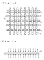
- An AC type plasma display panel (hereinafter called the PDP) as shown in Fig.7 has been known as an example of gas discharge panel.
- Fig.20 is a perspective sectional view schematically showing the PDP of the prior art.
- reference numeral 4 denotes a front substrate (also called the upper panel substrate), and 8 denotes a back substrate (also called the lower panel substrate).
- An outer casing 10 has such a configuration that the front substrate 4 and the back substrate 8 are disposed to oppose each other with the gap between the peripheries thereof being filled with a sealing member 9 (refer to Fig.21) made of glass having a low melting point thereby to form a gas discharge space which is sealed to be airtight and is filled with a rare gas (a mixture of helium and xenon gases) with a pressure from 4 x 10 4 to 7 x 10 4 Pa (300 to 500 Torr).
- a rare gas a mixture of helium and xenon gases
- the front substrate 4 comprises a front panel glass 201, display electrodes 1 formed in a pattern on the front panel glass 201, a dielectric film 2 formed to cover the display electrodes 1 and an MgO protective film 3 formed on the dielectric film 2.
- the back substrate 8 comprises a back panel glass 202, address electrodes 5 (also called the data electrode) formed in a pattern on the surface of the back panel glass 202, a dielectric film 6 formed to cover the address electrodes, division walls 7 comprising a plurality of ribs, and RGB fluorescent substances 11a through 11c applied between the ribs.
- the division wall 7 is means for dividing the gas discharge space. Compartment 12 thus divided serve as light emitting regions, while the fluorescent substance 11 is coated separately in each of these light emitting regions.
- the ribs of the division walls 7 and the address electrodes 5 are formed in parallel with each other and the display electrodes 1 and the address electrodes 5 cross at right angles with each other.
- the front panel glass and the back panel glass are sealed to form a space delimited thereby that is filled with the discharge gas. Because pressure of the discharge gas filling the space is usually lower than the atmospheric pressure, however, the front panel glass and the back panel glass are pressed inward by the atmospheric pressure so that ridges of the division walls 7, or top portions of the ribs, make contact with the inner surface of the front panel glass 201, thereby keeping the clearance between the front panel glass 201 and the hack panel glass 202. As a consequence, it is not necessary to bond the ridges of the division walls 7 and the inner surface of the front panel glass 201, which are merely brought into contact with each other.
- Fig.21 is a partially cutaway perspective view schematically showing the same PDP of the prior art as shown in Fig.20.
- the front substrate 4 is made by forming the electrodes 1 on the glass substrate 201, forming the dielectric film 2 to cover the electrodes 1, firing the dielectric film 2 and forming the protective film (MgO) 3 thereon by EB vapor deposition.
- the electrodes 5 are formed on a glass substrate 202 and is then covered the dielectric film 6 formed thereon and fired. Then after forming a layer of a material to make the division walls all over the surface by printing process, the division wall material is removed by sand blast from portions where the division wall is not to be formed thereby to form the division walls 7 in linear configuration through a firing process. Then the space between the ribs of the division walls 7 is filled with the fluorescent substance 11 by a printing process or the like, dried and fired to complete the back substrate 8.
- the front substrate 4 and the back substrate 8 completed as described above are fired after applying glass of low melting point that makes the sealing member 9 to the peripheries thereof, thereby sealing the space therebetween.
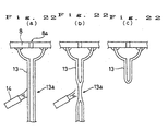
- a chip tube also called the piping member 13
- the space is filled with a rare gas and the tube is chipped off, thereby completing the PDP.
- the lower panel substrate 8 when manufacturing the PDP (container filled with the gas) of the prior art, the lower panel substrate 8 is fitted on an external position thereof with the piping member 13 that communicates with the gas discharge space in the casing 10 via a through hole 8a formed in the lower panel substrate 8. Then after purging the air from the inside of the casing (the container before being filled with the gas) 10 and filling the inner space with the discharge gas, the piping member 13 is closed thereby sealing the inner space of the casing 10.
- Closing of the piping member 13 is carried out as shown in Fig.22(a) by heating and melting the closing portion 13a of the piping member 13 with a gas burner 14 or the like applied from the outside. After causing the piping member 13 to contract by moving the lower portion of the closing portion 13a which has melted away from the casing 10 as shown in Fig.22(b), the piping member 13 is cut off by melting as shown in Fig.22(c).
- the closing portion 13a of the piping member 13 which has contracted is completely closed due to contraction of the inner wall of the piping.
- the lower panel substrate 8 bears the piping member 13, that was used when purging air from the inner space of the casing 10 and filling it with the discharge gas, remaining thereon as bonded by using the same material as the sealing member 9.
- the front substrate 4 and the back substrate 8 are bonded to each other on the peripheries thereof by frit glass (sealing member 9) used for sealing but mostly secured'by the differential pressure between the atmospheric pressure acting thereon from the outside and the inner pressure which is below one atmosphere of the gas filing the space between the front substrate and the back substrate, that causes the front substrate to be pressed against the division walls thereby to maintain the configuration.
- frit glass sealing member 9 used for sealing but mostly secured'by the differential pressure between the atmospheric pressure acting thereon from the outside and the inner pressure which is below one atmosphere of the gas filing the space between the front substrate and the back substrate, that causes the front substrate to be pressed against the division walls thereby to maintain the configuration.
- Pressure of the filling gas is generally from 4 x 10 4 to 7 x 10 4 Pa (300 Torr to 500 Torr), which is not significantly different from the atmospheric pressure of 1 x 10 5 Pa (760 Torr).
- the PDP of the prior art configuration has problems such as the displayed image is disturbed due to vibration when used onboard vehicles such as trains and buses.
- manufacture of the PDP of the prior art involves many firing processes that require a significant number of electric furnaces, leading to high energy cost and making it difficult to achieve energy-efficient production.
- the PDP of the prior art configuration has also such a problem that satisfactory brightness cannot necessarily be achieved.
- the inner pressure of the discharge gas filing the inside of the casing 10 must be increased to a level above 7 x 10 4 Pa (500 Torr).
- Prior art WO 95/19027A mentioned above describes a method of manufacturing such a gas discharge display where the planar substrates are bonded to the division walls by a wafer bonding process so as to provide individual cavities which are filled with gas discharge materials, whereby the pressure within such a cavity can be substantially more than 1 x 10 5 Pa (1 atm).
- An object of the present invention is to solve the problems of the plasma display panel of the prior art described above and provide a gas discharge panel that is less prone to cross talk and is capable of producing more stable image than the prior art, and a method for manufacturing the same.
- Another object of the present invention is to solve the problems of the method for manufacturing the plasma display panel of the prior art described above, and provide a method for manufacturing a gas discharge panel that is capable of reducing the number of firing processes over the prior art.
- Another object of the present invention is to solve the problems of the plasma display panel of the prior art described above and provide a gas discharge panel that is capable of achieving higher brightness than the prior art, and a method for manufacturing the same.
- the present invention achieves its objects by providing a gas discharge panel comprising the features set out in independent claim 1.
- the present invention also provides a method of manufacturing a gas discharge panel comprising the features of claim 1 by the method claimed in independent claim 17.
- the gas discharge panel comprising:
- the bonding member used in the bonding process includes a light-transmitting material.
- the bonding member used in the bonding process includes a light-absorbing material, and the material for making said division wall includes a light-reflecting material.
- the width of bonding portion between the ridge of said division wall and said first panel substrate is controlled so that the bonding portion does not intrude into a light emitting region in the divided gas discharge space.
- the bonding member used in the bonding process includes fusible glass.
- the softening point of said bonding member is lower than the softening point of said division walls.
- the difference in the softening point of said bonding member and said division walls is not lower than 20 °C and not higher than 200°C.
- the division walls have holes on the ridges thereof and said bonding members infiltrates the holes.
- the division walls may be formed by thermal spray process.
- At least one of the ridge surface of said division walls and portions of the inner surface of said first panel substrate bonded to the ridges has irregular shape.
- all or a part of the ridges of said division walls are bonded onto the inner surface of said first panel substrate.
- said division walls are a plurality of long plate-shaped ribs disposed in parallel to each other, and the bonding is achieved by using bonding members formed linearly in a direction substantially at right angles with the longitudinal direction of said ribs.
- said bonding member includes a light-absorbing material.
- said first panel substrate includes first electrodes, and notation that part of the ridges of said division walls are bonded onto the inner surface of said first panel substrate means that said bonding is provided in the vicinity of said first electrode in the ridges of said division walls.
- the ridges of said division walls have recesses formed thereon, and said bonding is achieved by using said recesses.
- said division walls and said second panel substrate are bonded by using frit glass.
- the present invention also provides a method for manufacturing a gas discharge panel as claimed in claim 1, the method comprising the steps of:
- said assembling step to form the gas discharge panel is carried out by pressurizing said first panel substrate (4) and/or said second panel substrate (8) that oppose each other so that a pressure is applied at least to the portions where said bonding members (15) are provided.
- the pressurization may be carried out by utilizing the resilience of a spring member.
- the pressurization may also be carried out by utilizing the weight of a plate.
- the pressurization may also be carried out by interposing a shock absorber between said plate and said panel substrate
- said bonding member includes fusible glass, an organic binder and an organic solvent which is applied to the ridges of said division walls and/or the inner surface of said first panel substrate; and said method includes a heating process of heating the bonding member which has been applied to a temperature not lower than the melting point of the fusible glass.
- a temporary firing process may be provided between said application process and said heating process for heating said bonding member to such an extent as most of the organic binder and of the organic solvent included in the applied bonding member are removed; and the assembly process is provided between said temporary firing process and said heating process for assembling said first panel substrate and said second panel substrate into said gas discharge panel by means of said sealing portion.
- the manufacturing method further comprises:
- a thermal spray method is employed in said second process and/or said third process.
- said mask member includes a photosensitive material.
- said mask member is a photosensitive resin film.
- said division wall material includes fusible glass, and firing of said division walls and firing of said bonding member are carried out in the same process.
- the method includes a division wall forming process of forming said division walls on said second panel substrate; said attaching process applies fusible glass paste as said bonding member to the ridges of said division walls; and includes a firing process of firing the fusible glass paste, wherein part of said division walls have light reflectivity and said fusible glass paste has light absorbency, and wherein said firing process is a process of bonding the ridges of said division walls and the inner surface of the first panel substrate by using said fusible glass paste.
- said attaching process employs a screen printing method.
- a screen mask used in said screen printing method does not have a pattern.
- said first panel substrate has first electrodes; said second panel substrate has second electrodes and opposes said first panel substrate; and comprises a process of forming grooves by exposing a photosensitive material provided on said second panel substrate to light; and a thermal spray process of filling the grooves formed in the foregoing process with a dielectric material to form said division walls, followed by thermal spraying frit glass onto said division walls to form the bonding members, while coolant gas is caused to flow along the material ejected from a thermal spray nozzle to cool down the second panel substrate in said thermal spray process.
- said gas discharge panel has a dielectric film that covers said second electrodes and the material making said dielectric film and said division walls is alumina.
- said piping member is closed by heating said piping member and pressing said piping member from the outside toward the inside so that the piping member is blocked in the sealing process.
- the piping member is closed by heating said piping member to melt a sealing member housed in the piping member so that the piping member is blocked in the sealing process.
- the piping member is closed by surrounding said piping member with a tubular member and heating the portion of the piping member surrounded by said tubular member while pressing said piping member along the axial direction of said tubular member so that the portion of said piping member is blocked in the sealing process.
- Fig.1 is a schematic partial cutaway view of a plasma display panel (PDP) that is an embodiment of the gas discharge panel of the present invention. Reference will be taken to this drawing in the description of the PDP configuration according to this embodiment that follows.
- PDP plasma display panel
- This embodiment is basically the same as the configuration of the PDP of the prior art described above with reference to Fig.20, except for such points as a frit glass 31 is used as a bonding member of the present invention. Frit glass 31 will be described later.
- reference numeral 21 denotes a front panel glass and 22 denotes a back panel glass.
- the front panel glass 21 has display electrodes 24 patterned thereon, with a dielectric film 28 and a protective film 29 being stacked thereon, thereby forming a front substrate 104.
- the back substrate 108 comprises the back panel glass 22, address electrodes 23 patterned thereon, division walls 30 and a fluorescent substance 25.
- the division walls 30 are formed integrally with dielectric films that cover the address electrodes 23, and are formed by thermal spray of alumina in this embodiment. This embodiment is different from the configuration of Fig.20 also in that the division walls 30 are formed integrally with dielectric films as described above.
- the division walls 30 comprise a plurality of plate-shaped ribs.
- a PDP 100 is made in such a configuration as the front substrate 104 and the back substrate 108 are disposed to oppose each other, with the peripheries thereof being sealed with a sealing member (not shown) made of glass having a low melting point for forming a gas discharge space, while the sealed losed space is filled with a rare gas (mixture of helium gas and xenon gas) with a pressure exceeding 1 x 10 5 Pa (760 Torr).
- the division walls 30 are means for dividing the gas discharge space into compartments 112 which act as light emitting regions.
- the frit glass 31 is applied onto the ridges of the division walls 30 in advance in the manufacturing process. Then with the front substrate 104 and the back substrate 108 being disposed to oppose each other and the panel being sealed, the inner surface of the front substrate 104 and the ridges of the division walls 30 are bonded together with the molten frit glass 31.
- the division walls 30 have some small holes on the surface thereof. These holes occur when the division walls 30 are formed by thermal spraying. Since the molten frit glass 31 penetrates the holes in the division walls 30, strength of the division walls 30 increases and bonding strength of the two substrates 104, 108 increases.
- the division walls 30 and the dielectric film formed integrally with the division walls 30 can be made by printing or other method.
- the division walls'30 and the dielectric film that lies below thereof may be made of the same material or different materials.
- Fig.2 is a schematic partial sectional view of a PDP according to second embodiment of the gas discharge panel of the present invention. Configuration of the PDP according to this embodiment will be described below with reference to this drawing.
- Configuration of the PDP according to this embodiment is substantially the same as that shown in Fig.1, except that bottom portions of the division walls 50 are bonded onto the back substrate 108 by frit glass 52, and therefore description thereof will be omitted.
- the division walls 50 have the frit glass 31, 52 applied in advance to the bottom portions 50b and the ridges 50a thereof.
- the frit glass 31 used for bonding the inner surface of the front substrate 21 with the ridges 50a of the division walls 50 may be either applied to the ridges 50a of the division walls 50 or applied to the inner surface of the front substrate 21 in a pattern before putting them together.
- the frit glass 52 applied between the division walls 50 and the dielectric layer 53 is effective in case the division walls 50 and the dielectric layer 53 are made of different materials and are bonded together with a relatively weak bonding force. As the frit glass 52 infiltrates the holes formed in the division walls 50, it has an effect of reinforcing the division walls 50.
- the frit glass 52 may be either formed at the same time as the division walls 50 are formed, or formed in the specified pattern on the dielectric layer 53 in advance before forming the division walls 50 thereon.
- FIG.3 (a) through (e) schematically show processes of an embodiment of a method for manufacturing the gas discharge panel according to the present invention.
- the method for manufacturing the PDP according to this embodiment will be described below with reference to these drawings.
- reference numeral 61 denotes address electrodes and 62 denotes a back panel glass.
- the address electrodes 61 are formed in a pattern on the surface of the back panel glass 62.
- a dielectric film 63 is formed to cover the address electrodes 61 and the surface of the back panel glass 62.
- a resist 64 is then applied to the surface of the dielectric film 63 and is patterned through exposure to light as shown Fig.3(c).
- portions missing the resist 64 are filled with division walls 65 made mainly of alumina by thermal spraying, followed by filling with frit glass 66.
- the frit glass 66 may be applied either by thermal spraying or other method, for example printing or simple squeezing.
- the resist 64 is then removed to leave the frit glass 66 on the ridges of the division walls 65 as shown in Fig.3(e)
- the back substrate made through the series of processes described above is disposed to oppose the front substrate and fired, with these substrates being sealed to form a space which is then filled with a gas.
- the PDP of a configuration similar to those described in conjunction with the first and the second embodiments is made very easily wherein the front substrate and the back substrate are joined together on the ridges of the division walls 65.
- the firing processes can be combined into a single process by applying a fluorescent substance to the surface between the ribs of the division walls 65 after the division walls have been formed by thermal spraying and the frit glass has been applied, then firing the fluorescent substance and carrying out boding and sealing of the two substrates at the same time.
- the bonding member used for bonding the ridge of the division walls and the inner surface of the front substrate includes fusible glass, an organic binder and an organic solvent
- the preliminary firing process is provided after the application of the bonding member and before sealing of the panel.
- Fig.4 (a) through (e) are diagrams schematically showing processes according to one embodiment of a method for manufacturing the gas discharge panel of the present invention.
- the method for manufacturing the PDP according to this embodiment will be described below with reference to these drawings.
- reference numeral 71 denotes address electrodes
- 72 denotes a dielectric film
- 73 denotes back panel glass.
- a layer of a mixture of alumina and frit glass (denoted by reference numeral 701 in the drawing) is formed over the dielectric film 72, for the formation of division walls 74.
- a layer of frit glass 75 is formed over the surface as shown in Fig.4(b).
- the division walls 74 and the frit glass 75 are formed by thermal spraying.
- the frit glass 75 may also be formed by applying the glass by a printing process and then firing.
- a pattern is formed by exposure of a resist 76, a dry film or the like to light.
- the material is then removed by sand blast from portions where the resist 76 is not deposited thereby to form the division walls 74, as shown in Fig.4(d).
- the division walls 74 have the frit glass film described in conjunction with Fig.4(b) deposited on the ridges thereof.
- the front substrate and the back substrate are then sealed to assemble the panel by using the sealing member as shown in Fig.4(e), with the panel being sealed by firing while bonding with the division walls 74 at the same time. While the sealing operation and bonding of the ridges of the division walls 74 with the inner surface of the front substrate are preferably carried out simultaneously in view of energy saving in the manufacturing process, they may also be carried out in separate processes as a matter of course.
- the fluorescent substance 78 may be fired either during sealing or separately before sealing.
- Number of firing processes can be reduced also with this manufacturing method that provides great effects of reducing the manufacturing facilities and energy consumption.
- the mixture of alumina and frit glass is used as the material to make the division walls and the frit glass fills the voids of alumina during sealing, void ratio decreases and division walls with less outgassing can be achieved. As a consequence, it is made possible to decrease pollution due to impurity gas and elongate the service life of the panel.
- Fig.5 schematically shows a method forming the division walls by thermal spraying, which is an embodiment of a method for manufacturing the gas discharge panel according to the present invention.
- the thermal spray method of this embodiment will be described below with reference to this drawing.
- reference numeral 81 denotes a thermal spray torch and 82 denotes a coolant gas.
- the coolant gas 82 removes unnecessary heat generated by the thermal spray and keeps the substrate temperature within 200°C.
- Reference numeral 83 denotes a powdery material to make the division walls 84 that is supplied with frit glass 87.
- Reference numeral 86 denotes a dry film for masking portions where the division walls are not to be formed.
- Reference numeral 85 denotes the back panel glass, 89 denotes the address electrodes and 88 denotes the dielectric film.
- the material to make the division walls included in the molten powder 83 sprayed from the thermal spray torch 81 is deposited in gaps between the dry films 86 which have been exposed to light and developed, to form a film having thickness of about 60% of the gap depth, followed by spraying of the frit glass 87 to form a film. Because the thermal spray is applied while cooling with the coolant gas 82, the dry film 86 is cooled down to such a temperature that is not harmful. When the dry film is removed, the division walls 84 with the frit glass 87 layer formed thereon are obtained.
- the division walls with the frit glass layer formed on the ridges thereof can be formed by a very simple method, and therefore number of the firing processes can be reduced while providing great effects of reducing the manufacturing facilities and energy consumption.
- the front substrate and the back substrate are bonded together and therefore the panel does not swell at the middle unlike the prior art even when the inner pressure of the PDP increases.
- the manufacturing method of the present invention makes it possible to greatly reduce the number of the firing processes and provide great effects of reducing the manufacturing facilities and energy consumption.
- the PDP of the present invention has such a configuration as the division walls formed on the back substrate or on the front substrate are bonded to the other substrate by means of the frit glass.
- the manufacturing method is such that the division walls are formed by thermal spraying with the frit glass also being applied to the ridges thereof by thermal spraying, while bonding of the division walls and the front substrate, sealing of the back substrate and the front substrate and firing of the fluorescent substance are carried out simultaneously.
- the panel does not break nor swell even when the pressure of the gas that fills the inside the panel is higher than the atmospheric pressure.
- the problems including cross talk do not occur, while good image is obtained and higher safety is achieved even when used onboard an airplane or the like.
- the substrates do not deflect because the front substrate and the back substrate are bonded together, and therefore good image is obtained even when used onboard a train, automobile or the like.
- the pressure of the discharge gas that fills the inside can be made higher than the atmospheric pressure according to this embodiment, PDP of high brightness and high efficiency can be achieved.
- Fig.6 is a perspective cutaway view schematically showing the configuration of a key portion of the PDP according to one embodiment of the gas discharge panel of the present invention.
- Fig.7 is a sectional view according to a variation thereof.
- Fig.8 is a drawing showing a method for closing the piping member in the manufacture of the PDP according to this embodiment.
- Fig.9 through Fig.11 are drawings showing first through third variations of the method and procedure for closing the piping member.
- the casing 10 has such a configuration as the upper panel substrate 4 and the lower panel substrate 8 are disposed to oppose each other while peripheries of the two panel substrates 4, 8 are sealed with a sealing member 9 made of glass having a low melting-point, thereby forming a discharging space therein.
- the upper panel substrate 4 is a substrate made of glass having a plurality of display electrodes 1, the dielectric layer 2 made of glass having a low melting point covering the display electrodes 1 and a protective film 3 made of magnesium oxide in a thin film being formed on the inner surface thereof.
- the lower panel substrate 8 is a substrate made of glass having a plurality of data electrodes 5 disposed at right angles to the display electrodes 1 and a dielectric layer 6 made of glass having a low melting point being formed on the inner surface thereof, while division walls 7 made of glass having a low melting point are formed in parallel to each other at predetermined positions on the dielectric layer 6 in order to separate compartments of light emitting regions.
- the division walls 7 have, on the ridges thereof, bonding members 15 made of a material having a low melting point such as frit glass (melting point of about 450°C) or water glass having a melting point lower than that of the material making the division wall 7 which is from 500 to 600°C.
- the division walls 7 formed on the lower panel substrate 8 and the upper panel substrate 4 are bonded by the bonding member 15.
- the bonding member 15 may also be made of an ultraviolet adhesive having low hygroscopicity and less outgassing or a common sealing material used in vacuum applications.
- the bonding member 15 is made of a material having a melting point lower than that of the division walls 7 in this embodiment in consideration of the convenience in the manufacturing process, a common adhesive may also be used regardless of the melting point as long as the manufacturing process allows it.
- the bonding members 15 may not necessarily be provided along the entire length of the ribs of the division walls 7. That is, the bonding members 15 may be provided at separate predetermined positions, as a matter of course.
- the bonded portions 2a on the dielectric layer 2 of the upper panel substrate 4, namely the portions to be bonded with the ridges of the division walls 7 by means of the bonding members 15, and/or portions 6a of the dielectric layer 6 of the lower panel substrate 8 where the division walls 7 are to be formed, namely either one or both of the predetermined portions 2a, 6a of the dielectric layer 2 and the dielectric layer 6 may have rough surface with fine irregularities formed thereon. With this configuration, the rough surface provides an anchoring effect.
- bonding strength between the dielectric layer 2 of the upper panel substrate 4 and the ridges of the division walls 7 via the thin protective film 3 and the bonding member 15 and the bonding strength between the dielectric layer 6 of the lower panel substrate 8 and the bottom of the division walls 7 are increased.
- the rough surface may be provided by such a common method as masking the portions which are not to be roughened and applying sand blast.
- the dielectric layer 6 of the lower panel substrate 8 is covered by the fluorescent substance 11, the dielectric layer 6 may also be roughened over the entire surface thereof.
- the dielectric layer 6 in each light emitting region separated by the division walls 7 is coated with the fluorescent substance 11 in order to produce color display.
- the inner space of the casing 10 formed by bonding the upper panel substrate 4 and the division walls 7 of the lower panel substrate 8 via the bonding members 15 is filled with a discharge gas comprising a mixture of helium, xenon, neon or the like, with an inner pressure exceeding 1 x 10 5 Pa (760 Torr), for example from 1 x 10 5 Pa to 1.33 x 10 5 Pa (750 Torr to 1000 Torr).
- the lower panel substrate 8 bears the piping member 13, that was used when purging air from the inner space of the casing 10 and filling it with the discharge gas, remaining thereon as bonded by using the same material as the sealing member 9.
- PDPs may be used onboard airplanes or trains, and subject to changes in the atmospheric pressure during sharp ascent or sharp dive of an airplane or vibration of a running train. Even in such cases, provided that the upper panel substrate 4 and the lower panel substrate 8 that constitute the casing 10 are bonded together by the bonding members 15 provided on the ridges of the division walls 7, such a problem never occurs as the casing 10 swells toward the outside and deform when the atmospheric pressure changes or under the presence of vibration.
- the bonding members 15 made of a material having a low melting point such as frit glass is applied onto the ridges of the division walls 7 of the lower panel substrate 8.
- the bonding members 15 are applied by such a technique as screen printing or transferring by means of a stamper, the bonding members 15 may also be provided by lift-off or the like before applying the fluorescent substance 11 thereon. Also in case the division walls 7 are formed through a plurality of screen printing operations, the bonding members 15 can be provided by forming only the uppermost layer from frit glass or the like, or alternatively, the frit glass or the like that makes the bonding members 15 may be applied to predetermined portions of the upper panel substrate 4 which correspond to the division walls 7 provided on the lower panel substrate 8.
- the bonding members 15 may also be provided only on the ridges of the division walls 7 by screen printing, after making the screen plate through the entire surface of which the adhesive material can pass.
- the upper panel substrate 4 and the lower panel substrate 8 are disposed to oppose each other via the division walls 7 whereon the bonding members 15 are provided as described above, and the two panel substrates 4, 8 are heated with the sealing member 9 provided between the peripheries thereof.
- the upper panel substrate 4 and the lower panel substrate 8 are bonded together by the bonding members 15 that has melted in the heating process.
- the piping member 13 that communicates with the inside of the casing 10 via the through hole 8a formed in the lower panel substrate 8 that constitutes the casing 10 is attached at a place outside the lower panel substrate 8.
- the inside the casing 10 is evacuated of the air and is filled with the discharge gas.
- the piping member 13 is closed by a method, for example, shown in Fig.8.
- the piping member 13 that communicates with the inside of the casing 10 via the through hole 8a formed on the lower panel substrate 8 that constitutes the casing 10 is attached at a place outside the lower panel substrate 8.
- the casing 10 with the piping member 13 attached thereto is placed at a proper position in a pressured chamber 16, while heating means 17 such as an induction heater or an electric heater is disposed along the periphery of the closing portion 13a of the piping member 13.
- the inner pressure of the pressured chamber 16 is set to a level higher than the pressure of the discharge gas in the casing 10.
- the piping member 13 can be closed in a procedure similar to that of the prior art.
- the closing portion 13a of the piping member 13 is heated and melted by the heating means 17. As the lower portion of the closing portion 13a is pulled away from the casing 10, the closing portion 13a of the piping member 13 which has been cut off by melting is closed, thereby sealing the casing 10. While the piping member 13 is closed by setting the pressure acting on the outer surface of the casing 10 higher than the inner pressure of the discharge gas in this embodiment, it is not necessary to employ such a laborious method. It is a matter of course that the piping member 13 can be closed similarly to the prior art simply by setting the pressure acting on the piping member 13 higher than the discharge gas pressure that fills the casing 10.
- Fig.9(a) through Fig.9(c) show the first variation of the method and procedure of closing the piping member 13.
- This method uses a sealing jig 17 that has a projection 17a having a section of semicircular or triangular configuration formed thereon to press the piping member 13 along the radial direction from at least two directions opposing along the radial direction of the piping member 13, and has a function of heating the piping member 13 via the projection 17a.
- the piping member 13 that communicates with the inside of the casing 10 via the through hole 8a formed in the lower panel substrate 8 that is one of the panel substrates is attached and, after purging the air from the inside of the casing 10 and filling it with the discharge gas through the piping member 13, the projection 17a of the sealing jig 17 is pressed against the closing portion 13a of the piping member 13 as shown in Fig.
- the piping member 13 is heated while pressing the projection 17a of the sealing jig 17 thereto along the radial direction thereof as shown in Fig.9(b), thereby cutting off the piping member 13 by melting it with the heat as shown in Fig.9(c).
- the closing portion 13a is closed as a result of pressing the projection 17a against the piping member 13 which has been heated to melt, and therefore the piping member 13 can be easily closed thereby to seal the casing 10, despite the inner pressure of the casing 10 being higher than the atmospheric pressure.
- the piping member 13 may also be closed as in the second variation shown in Fig.10, where a heating jig 18 fitted on the piping member 13 from the outside thereof is heated by means of a gas burner 14 or the like to melt the closing portion 13a of the piping member 13, while forcing the lower portion of the closing portion 13a in the direction of arrow, thereby to twist off the closing portion 13a while forcing it toward the casing 10.
- the heating jig 18 may be anything that can prevent the piping member 13 from swelling toward the outside due to the inner pressure that is higher than the atmospheric pressure and, while being omitted in the drawing, may be made of a metallic wire mesh. In case the heating jig 18 is stuck with the piping member 13, the heating jig 18 is left stuck with the piping member 13 which causes no problem at all.
- the piping member 13 that communicates with the inside of the casing 10 via the through hole 8a formed in the lower panel substrate 8 that is one of the panel substrates is attached and, after purging the air from the inside of the casing 10 and filling it with the discharge gas through the piping member 13, the gas burner 14 or the like is used from the outside to heat and melt the sealing member 19 that has been formed in a short rod from a material having a melting point lower than that of the piping member 13 and housed in the piping member 13, thereby closing the piping member 13 as shown in Fig.11(b). Then unnecessary portion of the piping member 13 closed with the sealing member 19 is removed by cutting off or other method.
- the sealing member 19 may be either housed in the piping member 13 in advance, put into the piping member 13 that has been attached to the lower panel substrate 8, or made of a material mixed with a black pigment to have high heat absorbing characteristic and is melted by irradiation of laser light.
- the casing 10 is filled with the discharge gas with a pressure not higher than 0.66 x 10 5 Pa (500 Torr), it is common to employ the manufacturing method comprising processes similar to those of the prior art. But the method of this embodiment may also be employed even in such a case where the inner pressure of the casing 10 is lower than the external pressure. This is known not claimed as an embodiment of the present invention.
- the gas discharge panel according to the present invention is characterized by, for example, the panel substrates that constitute the casing that are bonded together via the bonding members provided on the ridges of the division walls, while the casing 10 is filled with the discharge gas of a pressure exceeding 1 x 10 5 Pa (760 Torr).
- the bonding member is preferably made of a material having a melting point lower than that of the division wall.
- the casing never deforms by swelling toward outside.
- the casing 10 is filled with the discharge gas with a pressure exceeding 1 x 10 5 Pa (760 Torr)
- there is such an advantage that brightness of the gas discharge panel is improved.
- the improvement in the brightness of the gas discharge panel is due to the improved gas discharge efficiency.
- the method for manufacturing the gas discharge panel according to the present invention is for such a case, for example, as the inner pressure of the casing is higher than the external pressure during manufacturing, and is characterized in that the piping member is closed while keeping the pressure acting on at least the piping member from the outside higher than the discharge gas pressure that fills the casing, or the piping member is closed by heating while pressing the piping member from at least two directions opposing along the radial direction of the piping member, or the piping member is closed by melting the sealing member housed in the piping member. According to these manufacturing methods, the piping member can be easily and surely closed even when the inner pressure of the casing is higher than the external pressure.
- the gas discharge panel of the present invention due to such a configuration as, for example, the panel substrates that constitute the casing are bonded together via the bonding members provided on the ridges of the division walls, such problems never occur as a gap is produced between the division walls and the panel substrate or the casing deforms by swelling toward the outside. Thus there occurs no problem even when the casing is filled with the discharge gas with a pressure exceeding 1 x 10 5 Pa (760 Torr), thus making it possible to improve the brightness of the gas discharge panel.
- the piping member can be easily and surely closed and therefore the gas discharge panel of improved brightness can be easily manufactured.
- the bonding members 15 can be formed on the ridges of the division walls 7 by, for example, screen printing or the like.
- the ridges of the division walls 7 are very narrow and long and it may be difficult to form the bonding members 15 uniformly thereon.
- the ridges may have uneven surfaces.
- the bonding member may not be formed on recessed portions on the ridges of the division walls 7, in which case the upper panel substrate 4 and the division wall 7 are not bonded together at the recessed portions, which may lead to deteriorated display quality at such portions.
- the bonding member 15 after bonding has a width larger than the width of the division wall 7, where the light emitting region as viewed from the outside of the upper panel substrate 4 becomes narrower thereby leading to a decrease in brightness.
- the sealing member 9 of the prior art is formed only on the periphery of the panel substrate, and pressure is applied only to the periphery of the panel substrate when sealing.
- the division walls 7 and the upper panel substrate 4 must be bonded surely by the bonding members 15 in order to make the casing that does not deform, reliable bonding may not be achieved in the display region inside the panel substrate by applying pressure only to the periphery of the panel substrate even with such a configuration.
- Fig.12 is a plan view showing the application of the bonding members 15, and Fig.14 is a plan view of a variation thereof.
- Fig.13 is a schematic sectional view for the explanation of the relationship between particle size of the bonding member and the division wall width of the PDP according to this embodiment.
- Fig.17 is a sectional view showing a method of applying pressure during sealing.
- Fig. 18 and Fig.19 are sectional views showing the method of pressurizing during sealing.
- the PDP according to this embodiment is as described with reference to Fig.6.
- the ridges of the division walls 7 bear the bonding members 15 made of a transparent material formed thereon linearly along the longitudinal direction of the division walls 7 as shown in Fig.12.
- the division walls 7 formed on the lower panel substrate 8 and the upper panel substrate 4 are bonded to each other via the bonding members 15.
- the bonding members 15 formed on the ridges of the division walls 7 may partially project beyond the division wall width due to unevenness in the amount of application or the like, as described previously. Also when an excessive amount is applied when bonding with the upper panel substrate 4, the bonding member may be spread on top of the division wall and intrude into the light emitting region beyond the width of the division wall.
- the bonding member 15 is made of a transparent material, a little amount of it intruding into the light emitting region does not block the emitted light and does not cause deterioration in the display quality, particularly brightness.
- the dielectric layer 6 in each light emitting region separated by the division walls 7 is coated with the fluorescent substance 11 to produce color display.
- the casing 10 comprising the upper panel substrate 4 and the division walls 7 provided on the lower panel substrate 8 bonded together via the bonding members 15 is filled with the discharge gas comprising a mixture of helium, xenon and neon at a pressure exceeding 1 x 10 5 Pa (760 Torr), for example from 1 x 10 5 Pa to 1,33 x 10 5 Pa (760 Torr to 1000 Torr).
- the frit glass which has been commonly used for the bonding member includes a material such as lead oxide and a filler such as ceramics added to control the thermal characteristics and to obtain desired bonding strength with the glass substrate.
- Fig.13 shows a case where maximum particle size D of the material such as the filler included in the bonding members 15 does not exceed the width W of the division walls 7.
- the bonding member 15 does not project beyond the width of the division wall when the largest particle is located at the center of the division wall 7. Even when the largest particle is formed at a position somewhat offset from the center of the division wall 7, it does not significantly come out of the width of the division wall.
- the PDP having good display characteristic can be obtained without covering the display region with the bonding members 15 after bonding the division walls 7 and the upper panel 4. What is important here is to keep the bonding members from significantly coming out of the width of the division wall after bonding, and this can be achieved with the configuration described above.
- the bonding member To keep the bonding members from significantly coming out of the width of the division wall means to keep the bonding member from having such a width that substantially decreases the fluorescent substance region of each compartment 12 (Fig.6).
- the fluorescent substance region is determined by the area of the compartment 12 where the fluorescent substance 11 is applied.
- the bonding member tends to be formed unevenly, there is a possibility that the division walls and the upper panel are bonded to each other only at a portion where the largest particle lies. For this reason, it is desirable that the maximum particle size included in the bonding member be 5 ⁇ m or less.
- width W of the rib of the division wall (Fig.13) is about 40 ⁇ m.
- the bonding members 15 described above are provided on the ridges of the division walls 7, the bonding members 15 are provided in linear configuration on the inner surface of the panel substrate 4. That is, as shown in Fig. 14, the bonding members 15 are formed linearly at the center between one set of display electrodes and an adjoining set of display electrodes which are disposed in a pair, in such a direction that crosses the division walls 7 formed on the lower panel substrate 8 substantially at right angles (for example substantially at right angles to the longitudinal direction of the division walls 7).
- the bonding members 15 may be formed either by screen printing or drawing with a dispenser or the like.
- the two panel substrates 4, 8 that oppose each other are bonded together at points where the bonding members 15 and the division walls cross. Since the bonding members 15 are formed on a plane, they can be formed easily, and alignment can also be easily done when sealing because both the division walls 7 and the sealing member 15 have linear configuration and cross each other. Bonding is also made more reliably.
- the bonding members 15 also have a function of visually separating pixels which adjoin each other in the longitudinal direction of the division walls 7, prevent the casing 10 from swelling toward outside and deforming, and have an effect of improving the contrast.
- the bonding members 15 may also be formed on the ridges of the division walls 7 formed on the lower panel substrate 8 without any problem, while proving more effective in achieving more reliable bonding because sufficient amount of the bonding member is formed in the bonding area.
- the contrast of the PDP can be improved further by making the bonding members 15 shown in Fig.13 and Fig.14 of a light absorbing material.
- a PDP according to another variation of the bonding members 15 will be described below with reference to Fig.15. While the bonding members 15 described above are provided on most part of the ridges of the division walls 7 for bonding with the upper panel substrate 4, bonding may not necessarily be done on most part and partial bonding shown in Fig.15 is also effective.
- the bonding has, as described repetitively above, in addition to the apparent effect of preventing the panel from swelling toward the outside and deforming, and effect of preventing cross talk from occurring between discharge cells by filing the gap between the ridges of the division walls and the upper panel substrate with the bonding member and completely separating the discharge cells.
- Fig.15 shows a case of uniform bonding in the vicinity of the display electrode 1
- bonding may not necessarily be uniform and may be provided only at portions where cross talk is likely to occur or may be done linearly on some part of the ridges of the division walls.
- the PDP according to this embodiment has, similarly to the prior art, the casing of such a configuration as the upper panel substrate 4 with a plurality of display electrodes 1 formed thereon and the lower panel substrate 8 with a plurality of data electrodes 5 and the division walls formed on the inner surface thereof in a direction at right angles to the display electrodes 1 are disposed to oppose each other, and the peripheries of the panels are sealed by the bonding member 15 made of glass having a low melting point.
- the division walls 7 have grooves on the ridges thereof, while the grooves are filled with the bonding members 15 thereby to bond the upper panel substrate 4 and the division walls 7 via the bonding members 15.
- the division walls 7 are formed as follows.
- a resin coat layer is formed by laminating a dry resist film on the lower panel substrate 8 and, after selective exposure by using an exposure mask, a negative pattern is made by development process. An opening of the pattern is filled with a paste by squeezing or the like to the same height as the surface of the resin coat layer. Then the lower panel substrate 8 is dried to remove the solvent included in the paste, upon which the paste is recessed at the middle.
- This recessed shape can be adjusted by controlling the amount of the solvent included in the paste, the amount of the filler or the opening configuration of the resin coat layer. Alternatively, the recessed shape can be made by machining the ridges of the division walls 7 by mechanical means, irradiating with laser light or the like.
- bonding area between the division walls 7 and the bonding members 15 increases leading to increased bonding strength and also increases the apparent area of light emitting due to decreased projection of the bonding members 15 beyond the width of the division walls.
- the upper panel substrate 4 with the display electrodes 1, the dielectric layer 2 and the protective layer 3 formed thereon and the lower panel substrate 8 with the data electrodes 5, the dielectric layer 6 and the division walls 7 formed and the fluorescent substance 11 applied thereon are prepared, and the bonding member 15 made of a material having a low melting point such as frit glass are provided on the ridges of the division walls 7.
- the bonding members 15 While screen printing or transfer by means of a stamper is employed for providing the bonding members 15, they can also be applied by lift-off or the like. Or, alternatively, the bonding members 15 may also be provided by forming frit glass layers on the ridges of the division walls 7. Such a method may also be employed as frit glass that would become the bonding members 15 is applied to predetermined portions of the upper panel substrate 4 that correspond to the division walls 7 provided on the lower panel substrate 8.
- the bonding members 15 may also be provided only on the ridges of the division walls 7 by screen printing, after making a screen through the entire surface of which the adhesive material can pass.
- the upper panel substrate 4 and the lower panel substrate 8 are disposed to oppose each other via the division walls 7 having the bonding members formed thereon as described above, and the sealing member 9 is interposed between the peripheries of the two panel substrates 4, 8.
- the upper panel substrate 4 and the lower panel substrate 8 are sealed on the peripheries thereof by the sealing member 9.
- the upper panel substrate 4 and the lower panel substrate 8 are bonded to each other by the bonding members 15 which have been melted by the heat in the display area at the center, thereby forming the casing 10.
- the lower panel substrate 8 is fitted on an external position thereof with the piping member 13 that communicates with the casing 10 via the through hole 8a formed on the lower panel substrate 8 that constitutes the casing 10. Then after purging the air from the inside of the casing 10 and filling the inner space with the discharge gas the piping member 13, the piping member 13 is closed thereby sealing the inner space of the casing 10, thus completing the PDP shown in Fig.6.
- the upper panel substrate 4 and the lower panel substrate 8 that constitute the casing 10 are tentatively secured at predetermined positional relationship and placed on a flat base 16.
- the pressurizing jig 23 comprises a spring receiver A (20), a spring receiver B (22), a spring 21 and a bolt 19, while the spring receiver A (20) and the spring receiver B (22) are separated with the spring 21 interposed therebetween.
- Pressurizing force of the spring 21 can be controlled by adjusting the position of the spring receiver B (22) by means of the bolt 19.
- the pressurizing jig 23 is inserted between the casing 10 and a frame 18 that is secured on the base 16 via supports 17, while adjusting the position of the spring receiver B (22) by means of the bolt 19 so that the total length of the pressurizing jig 23 becomes greater than the distance. Since the spring 21 is installed while being compressed, pressure is applied to the two panel substrates.
- Frit glass that makes the bonding members 15 and the sealing member 9 is normally used while being heated to 450°C and melted, and the spring 21 used herein is of course made of a material that does not lose resilience at 450°C.
- Inconel is used.
- the upper panel substrate 4 and the lower panel substrate 8 that constitute the casing 10 are tentatively secured in predetermined positional relationship and placed on the flat base 16. Then a shock absorber 24 made of a resilient material that does not change the characteristics thereof when heated to 450°C is placed to cover the entire of the casing 10.
- a shock absorber 24 steel wool or the like can be used.
- a plate 25 having a predetermined weight, uniform thickness and a size that covers the entire surface of the casing is placed on the shock absorber 24 that is placed on the casing 10. It is necessary to interposed the shock absorber 24 between the plate 25 and the casing 10, because a foreign matter interposed therebetween may generate uneven gap between the upper panel substrate 4 and the lower panel substrate 8 that constitute the casing 10 due to partially changed pressure and, in case the foreign matter is large, localized force may be applied eventually leading to breakage of the casing 10.
- the gas discharge panel according to the present invention has such an advantage that, because the upper panel substrate and the lower panel substrate that constitute the casing are bonded to each other via the bonding members, problems of gap being generated between the division walls and the panel substrate and the casing swelling toward the outside to deform never occur, even when the casing is filled with the discharge gas with a pressure exceeding 0,66 x 10 5 Pa (500 torr). According to the invention, the casing is filled with the discharge gas with a pressure exceeding even 1 x 10 5 Pa (760 Torr).
- the bonding member does not come out of the width of the division walls or, should it come out, it is made of a transparent material. Also forming the bonding members in a direction at right angles to the division walls has an effect of separating the pixels that adjoin each other in the direction of the division walls, thereby improving the contrast.
- the method for manufacturing the gas discharge panel according to the present invention has such an advantage that the division walls and the opposing panel substrate can be bonded uniformly over the entire area of the casing, and therefore the gas discharge panel of improved brightness can be easily manufactured.
- the invention is not limited to this configuration and a configuration without dielectric film may also be employed.
- gas discharge panel in the embodiments described above is PDP of AC type
- gas discharge panel is not limited to PDP of AC type and the present invention may also be applied to PDP of DC type, as a matter of course.
- the first panel substrate and the second panel substrate of the present invention correspond respectively to the front panel substrate and the back panel substrate in the embodiments described above.
- the present invention is not limited to this arrangement and may be embodied in such an arrangement as the first panel substrate corresponds to the back panel substrate and the second panel substrate corresponds to the front panel substrate.
- bases of the division walls rest on the inner surface of the front panel substrate and ridges of the division walls rest on the inner surface of the back panel substrate.
- a variation of the example shown in Fig.8 and Fig.9 is a method for manufacturing the gas discharge panel comprising the first panel substrate having the first electrode, the second panel substrate having the second electrode opposing the first panel substrate, the sealing portion provided between the peripheries of the two substrates for forming the gas discharge space between the first and second panel substrates and division walls provided on the second panel substrate to divide the gas discharge space
- the manufacturing method comprises an assembly process of assembling the first panel substrate and the second panel substrate into the gas discharge panel by means of the sealing portion, a process of attaching the piping member that communicates with the gas discharge space via a through hole formed in the first or the second panel substrate onto the panel substrate that has the through hole, a sealing process of filling the gas discharge space with the discharge gas by using the piping member and a sealing process of closing the piping member.
- the present invention provides a gas discharge panel capable of producing more stable image with less possibility of cross talk than the prior art, and a method for manufacturing the same.
- the present invention also provides a method for manufacturing the gas discharge panel that is capable of reducing the number of firing processes over the prior art.
- the present invention also provides a method for manufacturing the gas discharge panel that is capable of increasing the brightness over the prior art.
Description
a heating process of heating the bonding member which has been applied to a temperature not lower than the melting point of the fusible glass.
the assembly process is provided between said temporary firing process and said heating process for assembling said first panel substrate and said second panel substrate into said gas discharge panel by means of said sealing portion.
the manufacturing method further comprises:
- a first process of providing a mask member having a predetermined opening on said panel substrate; and
- a second process of providing said division wall forming
material in said opening, and the bonding member
attaching process comprises:
- a third process of disposing said bonding member on the ridges of said division walls formed in said second process by using said mask member; and
- a fourth process of removing the mask member
a division wall forming process of forming said division walls on said second panel substrate;
said attaching process applies fusible glass paste as said bonding member to the ridges of said division walls; and includes
a firing process of firing the fusible glass paste,
wherein part of said division walls have light reflectivity and said fusible glass paste has light absorbency, and
wherein said firing process is a process of bonding the ridges of said division walls and the inner surface of the first panel substrate by using said fusible glass paste.
said first panel substrate has first electrodes;
said second panel substrate has second electrodes and opposes said first panel substrate; and comprises
a process of forming grooves by exposing a photosensitive material provided on said second panel substrate to light; and
a thermal spray process of filling the grooves formed in the foregoing process with a dielectric material to form said division walls, followed by thermal spraying frit glass onto said division walls to form the bonding members,
while coolant gas is caused to flow along the material ejected from a thermal spray nozzle to cool down the second panel substrate in said thermal spray process.
- 1:
- Display electrode
- 2, 6:
- Dielectric film
- 3:
- Protective film
- 4:
- Upper panel substrate (Front substrate)
- 5:
- Address electrode
- 7:
- Division wall
- 8:
- Lower panel substrate (Back substrate)
- 10:
- Casing
- 11:
- Fluorescent substance
- 12:
- Compartment
- 13:
- Piping member
- 15:
- Bonding member
- 19:
- Sealing member
Claims (35)
- A gas discharge panel comprising:characterized in thata first panel substrate (4);a second panel substrate (8) opposing said first panel substrate;a sealing portion (9) provided between peripheries of the two substrates (4,8) for forming a gas discharge space (12) between said first and second panel substrates, said gas discharge space (12) is filled with a discharge gas with a pressure exceeding 1x10⁵ Pa (760 Torr); anddivision walls (7) provided on said second panel substrate for dividing said gas discharge space,
ridges of said division walls (7) are bonded onto the inner surface of said first panel substrate (4) via bonding members (15). - A gas discharge panel as claimed in claim 1, wherein the bonding member (15) used in the bonding process includes a light-transmitting material.
- A gas discharge panel as claimed in claim 1, wherein the bonding member (15) used in the bonding process includes a light-absorbing material, and the material for making said division wall (7) includes a light-reflecting material.
- A gas discharge panel as claimed in claim 1, 2 or 3, wherein the width (D) of bonding portion (15) between the ridge of said division wall and said first panel substrate is controlled so that the bonding portion does not intrude into a light emitting region in the divided gas discharge space (12).
- A gas discharge panel as claimed in claim 1, wherein the bonding member (15) used in the bonding process includes fusible glass.
- A gas discharge panel as claimed in claim 1 wherein the softening point of said bonding member (15) is lower than the softening point of said division walls (7).
- A gas discharge panel as claimed in claim 6, wherein difference in the softening point of said bonding member (15) and said division walls (7) is not lower than 20 °C and not higher than 200 °C.
- A gas discharge panel as claimed in claim 5, wherein said division walls (7) have holes on the ridges thereof and said bonding members (15) infiltrates the holes.
- A gas discharge panel as claimed in claim 5 or 8, wherein said division walls (7) are formed by thermal spray process.
- A gas discharge panel as claimed in claim 1 or 5, wherein at least one of the ridge surface of said division walls (7) and portions (2a) of the inner surface of said first panel substrate bonded to the ridges has irregular shape.
- A gas discharge panel as claimed in claim 1 wherein all or a part of the ridges of said division walls (7) are bonded onto the inner surface of said first panel substrate (4).
- A gas discharge panel as claimed in claim 11 wherein said division walls are a plurality of long plate-shaped ribs (7) disposed in parallel to each other, and the bonding is achieved by using bonding members (15) formed linearly in a direction substantially at right angles with the longitudinal direction of said ribs.
- A gas discharge panel as claimed in claim 12, wherein said bonding member (15) includes a light-absorbing material.
- A gas discharge panel as claimed in claim 11, 12 or 13, wherein said first panel substrate (4) includes first electrodes and notation that part of the ridges of said division walls (7) are bonded onto the inner surface of said first panel substrate (4) means that said bonding in the ridges of said division walls is provided in the vicinity of said first electrodes (1).
- A gas discharge panel as claimed in claim 1 wherein the ridges of said division walls (7) have recesses formed thereon, and said bonding is achieved by using said recesses.
- A gas discharge panel as claimed in claim 1, wherein said division walls (50) and said second panel substrate (108) are bonded by using frit glass (52).
- A method for manufacturing a gas discharge panel according to claim 1,
characterized by
comprising the process steps of:attaching the bonding members onto the ridges of said division walls (7) or onto the inner surface of said first panel substrate (4);assembling said first panel substrate (4) and said second panel substrate (8) into said gas discharge panel by means of said sealing portion (9);bonding the ridges of said division walls (7) and said first panel substrate (4) by means of said bonding members (15); and bya process of attaching a piping member (13), that communicates with the gas discharge space (12) via a through hole (8a) formed in said first or second panel substrate, onto the panel substrate that has said through hole;a filling process of filling said gas discharge space (12) with the discharge gas with a pressure exceeding 1x10⁵ Pa (760 Torr) by using said piping member (13); anda sealing process of closing said piping member (13) by setting the pressure surrounding said piping member higher than the inner pressure of the discharge gas that fills the gas discharge space. - A method for manufacturing the gas discharge panel as claimed in claim 17, wherein said piping member (13) is closed by heating said piping member (13) and pressing said piping member from the outside toward the inside so that the piping member is blocked in the sealing process.
- A method for manufacturing the gas discharge panel as claimed in claim 17, wherein the piping member (13) is closed by heating said piping member to melt a sealing member (19) housed in the piping member so that the piping member is blocked in the sealing process.
- A method for manufacturing the gas discharge panel as claimed in claim 17, wherein the piping member (13) is closed by surrounding said piping member with a tubular member (18) and heating the portion of the piping member surrounded by said tubular member while pressing said piping member along the axial direction of said tubular member so that the portion of said piping member is blocked in the sealing process.
- A method for manufacturing the gas discharge panel as claimed in claim 17, wherein said assembling step to form said gas discharge panel is carried out by pressurizing said first panel substrate (4) and/or said second panel substrate (8) that oppose each other so that a pressure is applied at least to the portions where said bonding members (15) are provided.
- A method for manufacturing a gas discharge panel as claimed in claim 21, wherein the pressurization is carried out by utilizing the resilience of a spring.
- A method for manufacturing the gas discharge panel as claimed in claim 21, wherein the pressurization is carried out by utilizing the weight of a plate (25) and a shock absorber (24) is interposed between said plate and said panel substrate.
- A method for manufacturing the gas discharge panel as claimed in claim 17, wherein said bonding member (15) includes fusible glass, an organic binder and an organic solvent; and said method includes a heating process for heating the bonding member (15) to a temperature not lower than the melting point of the fusible glass to bond said bonding member to said first panel substrate.
- A method for manufacturing the gas discharge panel as claimed in claim 24 further comprising:a temporary firing process provided between said attaching process and said heating process for heating said bonding member (15) to such an extent as most of the organic binder and of the organic solvent included in the applied bonding member are removed; andsaid assembly process is provided between said temporary firing process and said heating process for assembling said first panel substrate (4) and said second panel substrate (8) into said gas discharge panel by means of said sealing portion (9).
- A method for manufacturing the gas discharge panel as claimed in claim 17, further comprising the process steps of:a division wall forming process of forming said division walls on said second panel substrate, wherein the division wall forming process comprises:a first process of providing a mask member (64) having a predetermined opening on said panel substrate; and a second process of providing a division wall forming material (65) in said opening, and the bonding member attaching process comprises:a third process of disposing said bonding member (66) on the ridges of said division walls formed in the second process by using said mask member (64); anda fourth process of removing said mask member (64).
- A method for manufacturing the gas discharge panel as claimed in claim 26, wherein a thermal spray method is employed in said second process and/or said third process.
- A method for manufacturing the gas discharge panel as claimed in claim 26 or 27, wherein said mask member (64) includes a photosensitive material.
- A method for manufacturing the gas discharge panel as claimed in claim 28, wherein said mask member (64) is a photosensitive resin film.
- A method for manufacturing the gas discharge panel as claimed in claim 26 or 27, wherein said division wall material includes fusible glass, and firing of said division walls and firing of said bonding member are carried out in the same process.
- A method for manufacturing the gas discharge panel as claimed in claim 17, further comprising the process steps of:a division wall forming process for forming said division walls on said second panel substrate; andsaid attaching process applies fusible glass paste as said bonding members to the ridges of said division walls; and includesa firing process of firing the fusible glass paste, wherein the process materials are such that part of the division walls have light reflectivity and said fusible glass paste has light absorbency.
- A method for manufacturing the gas discharge panel as claimed in claim 17, wherein said first panel substrate has first electrodes and said second panel substrate has second electrodes, said method further comprising the process steps of:a process of forming grooves by exposing a photosensitive material (86) provided on said second panel substrate (85) to light; and a thermal spray process of filling the grooves formed in the foregoing process with a dielectric material (88) to form said division walls (84) followed by thermal spraying frit glass (87) onto said division walls to form said bonding members (87),while coolant gas (82) is caused to flow along the material ejected from a thermal spray nozzle (81) to cool down the second panel substrate in said thermal spray process.
- A method for manufacturing the gas discharge panel as claimed in claim 32, wherein said gas discharge panel has a dielectric film (88) that covers said second electrodes (89) and the material making said dielectric film and said division walls is alumina.
- A method for manufacturing the gas discharge panel as claimed in claim 17, wherein the process of providing said bonding members employs screen printing method.
- A method for manufacturing the gas discharge panel as claimed in claim 34, wherein a screen mask used in said screen printing method does not have a pattern.
Applications Claiming Priority (11)
| Application Number | Priority Date | Filing Date | Title |
|---|---|---|---|
| JP33556396 | 1996-12-16 | ||
| JP33556396 | 1996-12-16 | ||
| JP4900697 | 1997-03-04 | ||
| JP4900697 | 1997-03-04 | ||
| JP22221297 | 1997-08-19 | ||
| JP22221297 | 1997-08-19 | ||
| JP28171697 | 1997-10-15 | ||
| JP28171697 | 1997-10-15 | ||
| JP31493897 | 1997-11-17 | ||
| JP31493897 | 1997-11-17 | ||
| PCT/JP1997/004598 WO1998027571A1 (en) | 1996-12-16 | 1997-12-12 | Gaseous discharge panel and manufacturing method therefor |
Publications (3)
| Publication Number | Publication Date |
|---|---|
| EP0945886A1 EP0945886A1 (en) | 1999-09-29 |
| EP0945886A4 EP0945886A4 (en) | 2000-07-26 |
| EP0945886B1 true EP0945886B1 (en) | 2005-03-02 |
Family
ID=27522767
Family Applications (1)
| Application Number | Title | Priority Date | Filing Date |
|---|---|---|---|
| EP97947930A Expired - Lifetime EP0945886B1 (en) | 1996-12-16 | 1997-12-12 | Gaseous discharge panel and manufacturing method therefor |
Country Status (6)
| Country | Link |
|---|---|
| US (2) | US6353287B1 (en) |
| EP (1) | EP0945886B1 (en) |
| KR (1) | KR100376037B1 (en) |
| CN (2) | CN100382224C (en) |
| DE (1) | DE69732646T2 (en) |
| WO (1) | WO1998027571A1 (en) |
Families Citing this family (33)
| Publication number | Priority date | Publication date | Assignee | Title |
|---|---|---|---|---|
| US6540576B1 (en) * | 1997-10-16 | 2003-04-01 | Matsushita Electric Industrial Co., Ltd. | Plasma display panel and method of manufacturing the same |
| EP1110231B1 (en) | 1998-09-08 | 2006-07-12 | Matsushita Electric Industrial Co., Ltd. | Display panel manufacturing method including bonding agent application method |
| DE69942894D1 (en) * | 1998-09-14 | 2010-12-09 | Panasonic Corp | SEALING METHOD AND DEVICE FOR PRODUCING HIGH-PERFORMANCE GAS DISCHARGE DISPLAY EQUIPMENT |
| US6848964B1 (en) | 1998-09-14 | 2005-02-01 | Matsushita Electric Industrial Co., Ltd. | Sealing method and apparatus for manufacturing high-performance gas discharge panel |
| JP3437100B2 (en) * | 1998-09-30 | 2003-08-18 | 三菱電機株式会社 | Display panel |
| EP1720150A3 (en) * | 1998-11-13 | 2007-08-08 | Matsushita Electric Industrial Co., Ltd. | High resolution and high luminance plasma display panel and drive method for the same |
| TW452812B (en) * | 1999-08-04 | 2001-09-01 | Koninkl Philips Electronics Nv | Plasma display panel |
| JP2001189136A (en) * | 1999-10-19 | 2001-07-10 | Matsushita Electric Ind Co Ltd | Plasma display device and its production |
| WO2001035437A1 (en) * | 1999-11-11 | 2001-05-17 | Matsushita Electric Industrial Co., Ltd. | Method and device for producing gas electric discharge panels |
| KR100313116B1 (en) * | 1999-12-10 | 2001-11-07 | 김순택 | Method for driving plasma display panel |
| KR100341840B1 (en) * | 1999-12-16 | 2002-06-24 | 구자홍 | Barrier rib molding equipment of Plasma display panel and Punch Processing Device for the same |
| TW472285B (en) * | 2000-03-17 | 2002-01-11 | Acer Display Tech Inc | Plasma display panel with tight sealing between two plates and the manufacturing method thereof |
| TW509960B (en) * | 2000-04-04 | 2002-11-11 | Matsushita Electric Ind Co Ltd | Highly productive method of producing plasma display panel |
| KR20020087495A (en) * | 2000-04-19 | 2002-11-22 | 마츠시타 덴끼 산교 가부시키가이샤 | Display panel and production method therefor |
| US6685523B2 (en) * | 2000-11-14 | 2004-02-03 | Plasmion Displays Llc | Method of fabricating capillary discharge plasma display panel using lift-off process |
| TW480516B (en) * | 2000-11-24 | 2002-03-21 | Acer Display Tech Inc | Front plate and rear plate structure of plasma display panel |
| JP4700204B2 (en) * | 2001-03-07 | 2011-06-15 | 株式会社日立製作所 | Storage management data control system |
| FR2831709A1 (en) * | 2001-10-29 | 2003-05-02 | Thomson Licensing Sa | PLASMA PANEL SLAB COMPRISING MEANS FOR RE-DISSEMINATING THE RADIATION EMITTED BY THE DISCHARGES |
| US6890445B2 (en) * | 2001-12-13 | 2005-05-10 | Agere Systems, Inc. | Process for packaging electronic devices using thin bonding regions |
| DE10225612A1 (en) * | 2002-06-07 | 2003-12-18 | Patent Treuhand Ges Fuer Elektrische Gluehlampen Mbh | Manufacturing system for gas discharge lamp has inner chamber with electrodes in communication with outer chamber which may be flushed out with different mixtures of gases |
| JP3944148B2 (en) * | 2002-10-31 | 2007-07-11 | キヤノン株式会社 | Manufacturing method of image display device |
| JP3994998B2 (en) * | 2004-03-03 | 2007-10-24 | セイコーエプソン株式会社 | LIGHT EMITTING DEVICE, LIGHT EMITTING DEVICE MANUFACTURING METHOD, AND ELECTRONIC DEVICE |
| KR100635222B1 (en) * | 2004-05-19 | 2006-10-17 | 주식회사 에이디피엔지니어링 | Apparatus for attaching ??? substrate and Method for attaching ??? substrate |
| KR100774962B1 (en) * | 2005-02-01 | 2007-11-09 | 엘지전자 주식회사 | Plasma Display Panel and Making method thereof |
| KR20060098459A (en) * | 2005-03-03 | 2006-09-19 | 삼성에스디아이 주식회사 | Structure of dielectric layer for plasma display panel and plasma display panel comprising the same |
| JPWO2007023564A1 (en) * | 2005-08-26 | 2009-02-26 | 日立プラズマディスプレイ株式会社 | Plasma display panel and manufacturing method thereof |
| CN100452281C (en) * | 2006-01-11 | 2009-01-14 | 四川世纪双虹显示器件有限公司 | Method for making plasma display screen lower substrate |
| KR100730200B1 (en) * | 2006-02-07 | 2007-06-19 | 삼성에스디아이 주식회사 | Plasma display panel |
| KR20080105787A (en) * | 2007-06-01 | 2008-12-04 | 엘지전자 주식회사 | Plasma display panel and method for fabricating the same |
| KR100824705B1 (en) * | 2007-09-05 | 2008-04-24 | (주)제이스 | Plasma display panel and fabrication method thereof |
| WO2011105036A1 (en) * | 2010-02-25 | 2011-09-01 | パナソニック株式会社 | Plasma display panel and manufacturing method thereof |
| CN103500694A (en) * | 2013-09-26 | 2014-01-08 | 四川虹欧显示器件有限公司 | PDP (Plasma Display Panel) screen gas charging method and PDP screen based on same |
| KR102240894B1 (en) * | 2014-02-26 | 2021-04-16 | 삼성디스플레이 주식회사 | Display device and method of manufacturing a display device |
Family Cites Families (32)
| Publication number | Priority date | Publication date | Assignee | Title |
|---|---|---|---|---|
| JPS50100967A (en) | 1973-12-07 | 1975-08-11 | ||
| JPS5647662B2 (en) * | 1974-06-12 | 1981-11-11 | ||
| JPS598934B2 (en) | 1976-08-26 | 1984-02-28 | 旭硝子株式会社 | Manufacturing method of glass substrate for panel display device |
| JPS54158859A (en) | 1978-06-06 | 1979-12-15 | Fujitsu Ltd | Plasma display panel |
| JPS6064659A (en) | 1983-09-20 | 1985-04-13 | Toshiba Corp | Plasma spraying jig |
| JPS638044A (en) * | 1986-06-27 | 1988-01-13 | Toyoda Gosei Co Ltd | Side molding and its manufacture |
| JPH0652599B2 (en) | 1987-10-28 | 1994-07-06 | 株式会社日立製作所 | Cam mechanism of magnetic recording / reproducing device |
| JPH01113848A (en) | 1987-10-28 | 1989-05-02 | Fujitsu Ltd | Access control system |
| JPH01113948U (en) * | 1988-01-26 | 1989-07-31 | ||
| JP3037701B2 (en) | 1989-03-16 | 2000-05-08 | 大日本印刷株式会社 | Plasma display panel and method of manufacturing the same |
| JPH03254041A (en) | 1990-03-05 | 1991-11-13 | Mitsubishi Electric Corp | Manufacture of display device |
| JP2596279B2 (en) | 1992-01-30 | 1997-04-02 | 双葉電子工業株式会社 | Enclosure support pillar formation method |
| SE9201768L (en) | 1992-06-09 | 1993-12-10 | Electrolux Ab | Refrigerator with intermittent sorption chiller |
| US5438343A (en) | 1992-07-28 | 1995-08-01 | Philips Electronics North America Corporation | Gas discharge displays and methodology for fabricating same by micromachining technology |
| GB2276270A (en) * | 1993-03-18 | 1994-09-21 | Ibm | Spacers for flat panel displays |
| US5777436A (en) * | 1994-05-25 | 1998-07-07 | Spectron Corporation Of America, L.L.C. | Gas discharge flat-panel display and method for making the same |
| US5469021A (en) * | 1993-06-02 | 1995-11-21 | Btl Fellows Company, Llc | Gas discharge flat-panel display and method for making the same |
| JP3292434B2 (en) | 1994-10-17 | 2002-06-17 | 太陽インキ製造株式会社 | Composition for forming partition of plasma display panel and method of forming partition using the same |
| JP3329109B2 (en) * | 1994-12-02 | 2002-09-30 | ソニー株式会社 | Plasma address display |
| JPH08185802A (en) | 1994-12-28 | 1996-07-16 | Noritake Co Ltd | Discharge display device |
| JP3224486B2 (en) * | 1995-03-15 | 2001-10-29 | パイオニア株式会社 | Surface discharge type plasma display panel |
| JP3212837B2 (en) * | 1995-06-30 | 2001-09-25 | 富士通株式会社 | Plasma display panel and method of manufacturing the same |
| US5982095A (en) * | 1995-09-19 | 1999-11-09 | Lucent Technologies Inc. | Plasma displays having electrodes of low-electron affinity materials |
| KR19980065367A (en) * | 1996-06-02 | 1998-10-15 | 오평희 | Backlight for LCD |
| JP3739163B2 (en) * | 1997-03-31 | 2006-01-25 | 三菱電機株式会社 | Plasma display panel |
| US6160348A (en) * | 1998-05-18 | 2000-12-12 | Hyundai Electronics America, Inc. | DC plasma display panel and methods for making same |
| JP3428446B2 (en) * | 1998-07-09 | 2003-07-22 | 富士通株式会社 | Plasma display panel and method of manufacturing the same |
| JP3706742B2 (en) * | 1998-07-15 | 2005-10-19 | パイオニア株式会社 | Plasma display panel |
| JP3442294B2 (en) * | 1998-09-29 | 2003-09-02 | 三菱電機株式会社 | Flat panel |
| KR100295112B1 (en) * | 1998-12-02 | 2001-07-12 | 구자홍 | Lower substrate for plasma display device |
| US6544090B1 (en) * | 2000-06-16 | 2003-04-08 | E. I. Du Pont De Nemours And Company | Method for forming barrier structures on a substrate and the resulting article |
| TW454217B (en) * | 2000-07-21 | 2001-09-11 | Acer Display Tech Inc | Flat panel display having sealing glass of guiding slot |
-
1997
- 1997-12-12 CN CNB021427186A patent/CN100382224C/en not_active Expired - Fee Related
- 1997-12-12 US US09/331,139 patent/US6353287B1/en not_active Expired - Fee Related
- 1997-12-12 CN CNB97180625XA patent/CN1147906C/en not_active Expired - Fee Related
- 1997-12-12 DE DE69732646T patent/DE69732646T2/en not_active Expired - Fee Related
- 1997-12-12 KR KR10-1999-7005431A patent/KR100376037B1/en not_active IP Right Cessation
- 1997-12-12 EP EP97947930A patent/EP0945886B1/en not_active Expired - Lifetime
- 1997-12-12 WO PCT/JP1997/004598 patent/WO1998027571A1/en active IP Right Grant
-
2001
- 2001-07-30 US US09/918,038 patent/US6758714B2/en not_active Expired - Fee Related
Also Published As
| Publication number | Publication date |
|---|---|
| CN1240534A (en) | 2000-01-05 |
| US6353287B1 (en) | 2002-03-05 |
| EP0945886A1 (en) | 1999-09-29 |
| CN1147906C (en) | 2004-04-28 |
| KR20000057633A (en) | 2000-09-25 |
| DE69732646T2 (en) | 2005-07-21 |
| EP0945886A4 (en) | 2000-07-26 |
| US6758714B2 (en) | 2004-07-06 |
| US20020017862A1 (en) | 2002-02-14 |
| CN1495824A (en) | 2004-05-12 |
| DE69732646D1 (en) | 2005-04-07 |
| CN100382224C (en) | 2008-04-16 |
| KR100376037B1 (en) | 2003-03-15 |
| WO1998027571A1 (en) | 1998-06-25 |
Similar Documents
| Publication | Publication Date | Title |
|---|---|---|
| EP0945886B1 (en) | Gaseous discharge panel and manufacturing method therefor | |
| JP3428446B2 (en) | Plasma display panel and method of manufacturing the same | |
| US7230381B2 (en) | Method of manufacturing a plasma display panel | |
| US6483238B1 (en) | Plasma display panel having a porous structure | |
| US6527606B1 (en) | Process for the manufacture of a plasma panel | |
| JP3466069B2 (en) | Gas discharge panel and method of manufacturing the same | |
| US8113899B2 (en) | Method for producing plasma display panel | |
| US6477863B1 (en) | Method for producing a dielectric coating comprising embossed patterns on a plasma panel faceplate | |
| JP2000149772A (en) | Manufacture of plasma display panel, plasma display panel, and substrate for plasma display panel | |
| JP2002072921A (en) | Display panel and producing method thereof | |
| JP3656072B2 (en) | Method for manufacturing gas discharge panel | |
| WO1999003126A1 (en) | Flashover controlling spacer for parallel plate electron beam device | |
| US5989089A (en) | Method of fabricating separator walls of a plasma display panel | |
| KR20080029751A (en) | Plasma display panel and manufacturing method thereof | |
| JP3614592B2 (en) | Method for forming partition wall of display panel | |
| JP2005056834A (en) | Method for manufacturing display panel | |
| KR100509599B1 (en) | Barrier for the plasma display panel and Method for the plasma display panel using the barrier | |
| JPH1040818A (en) | Plasma display panel and its manufacture | |
| KR100433220B1 (en) | Method of Fabricating Back Plate in Plasma Display Panel | |
| US20110279030A1 (en) | Plasma display panel and manufacturing method thereof | |
| EP1840927A2 (en) | Plasma display panel and manufacturing method thereof | |
| KR100452702B1 (en) | Method of Fabricating Rib of Plasma Display Panel | |
| JP2002184317A (en) | Plasma display panel substrate, plasma display panel and plasma display device | |
| JP2003123657A (en) | Plasma display panel and its manufacturing method | |
| JP2010146890A (en) | Method of manufacturing plasma display panel |
Legal Events
| Date | Code | Title | Description |
|---|---|---|---|
| PUAI | Public reference made under article 153(3) epc to a published international application that has entered the european phase |
Free format text: ORIGINAL CODE: 0009012 |
|
| 17P | Request for examination filed |
Effective date: 19990614 |
|
| AK | Designated contracting states |
Kind code of ref document: A1 Designated state(s): DE FR GB |
|
| A4 | Supplementary search report drawn up and despatched |
Effective date: 20000608 |
|
| AK | Designated contracting states |
Kind code of ref document: A4 Designated state(s): DE FR GB |
|
| RIC1 | Information provided on ipc code assigned before grant |
Free format text: 7H 01J 11/02 A, 7H 01J 17/16 B, 7H 01J 9/02 B, 7H 01J 9/26 B, 7H 01J 9/395 B, 7H 01J 17/49 B |
|
| 17Q | First examination report despatched |
Effective date: 20030305 |
|
| GRAP | Despatch of communication of intention to grant a patent |
Free format text: ORIGINAL CODE: EPIDOSNIGR1 |
|
| GRAS | Grant fee paid |
Free format text: ORIGINAL CODE: EPIDOSNIGR3 |
|
| GRAA | (expected) grant |
Free format text: ORIGINAL CODE: 0009210 |
|
| AK | Designated contracting states |
Kind code of ref document: B1 Designated state(s): DE FR GB |
|
| REG | Reference to a national code |
Ref country code: GB Ref legal event code: FG4D |
|
| REF | Corresponds to: |
Ref document number: 69732646 Country of ref document: DE Date of ref document: 20050407 Kind code of ref document: P |
|
| ET | Fr: translation filed | ||
| PLBE | No opposition filed within time limit |
Free format text: ORIGINAL CODE: 0009261 |
|
| STAA | Information on the status of an ep patent application or granted ep patent |
Free format text: STATUS: NO OPPOSITION FILED WITHIN TIME LIMIT |
|
| 26N | No opposition filed |
Effective date: 20051205 |
|
| PGFP | Annual fee paid to national office [announced via postgrant information from national office to epo] |
Ref country code: GB Payment date: 20061206 Year of fee payment: 10 |
|
| PGFP | Annual fee paid to national office [announced via postgrant information from national office to epo] |
Ref country code: DE Payment date: 20061207 Year of fee payment: 10 |
|
| PGFP | Annual fee paid to national office [announced via postgrant information from national office to epo] |
Ref country code: FR Payment date: 20061208 Year of fee payment: 10 |
|
| GBPC | Gb: european patent ceased through non-payment of renewal fee |
Effective date: 20071212 |
|
| PG25 | Lapsed in a contracting state [announced via postgrant information from national office to epo] |
Ref country code: DE Free format text: LAPSE BECAUSE OF NON-PAYMENT OF DUE FEES Effective date: 20080701 |
|
| REG | Reference to a national code |
Ref country code: FR Ref legal event code: ST Effective date: 20081020 |
|
| PG25 | Lapsed in a contracting state [announced via postgrant information from national office to epo] |
Ref country code: GB Free format text: LAPSE BECAUSE OF NON-PAYMENT OF DUE FEES Effective date: 20071212 |
|
| PG25 | Lapsed in a contracting state [announced via postgrant information from national office to epo] |
Ref country code: FR Free format text: LAPSE BECAUSE OF NON-PAYMENT OF DUE FEES Effective date: 20071231 |