EP0908902A2 - PTC-element, protective device and electric circuit board - Google Patents
PTC-element, protective device and electric circuit board Download PDFInfo
- Publication number
- EP0908902A2 EP0908902A2 EP98308088A EP98308088A EP0908902A2 EP 0908902 A2 EP0908902 A2 EP 0908902A2 EP 98308088 A EP98308088 A EP 98308088A EP 98308088 A EP98308088 A EP 98308088A EP 0908902 A2 EP0908902 A2 EP 0908902A2
- Authority
- EP
- European Patent Office
- Prior art keywords
- ptc
- conductor material
- protective device
- crystalline polymer
- conductive crystalline
- Prior art date
- Legal status (The legal status is an assumption and is not a legal conclusion. Google has not performed a legal analysis and makes no representation as to the accuracy of the status listed.)
- Granted
Links
Images


Classifications
-
- H—ELECTRICITY
- H01—ELECTRIC ELEMENTS
- H01C—RESISTORS
- H01C7/00—Non-adjustable resistors formed as one or more layers or coatings; Non-adjustable resistors made from powdered conducting material or powdered semi-conducting material with or without insulating material
- H01C7/02—Non-adjustable resistors formed as one or more layers or coatings; Non-adjustable resistors made from powdered conducting material or powdered semi-conducting material with or without insulating material having positive temperature coefficient
- H01C7/027—Non-adjustable resistors formed as one or more layers or coatings; Non-adjustable resistors made from powdered conducting material or powdered semi-conducting material with or without insulating material having positive temperature coefficient consisting of conducting or semi-conducting material dispersed in a non-conductive organic material
-
- H—ELECTRICITY
- H01—ELECTRIC ELEMENTS
- H01H—ELECTRIC SWITCHES; RELAYS; SELECTORS; EMERGENCY PROTECTIVE DEVICES
- H01H85/00—Protective devices in which the current flows through a part of fusible material and this current is interrupted by displacement of the fusible material when this current becomes excessive
- H01H85/02—Details
- H01H85/46—Circuit arrangements not adapted to a particular application of the protective device
- H01H2085/466—Circuit arrangements not adapted to a particular application of the protective device with remote controlled forced fusing
-
- H—ELECTRICITY
- H01—ELECTRIC ELEMENTS
- H01L—SEMICONDUCTOR DEVICES NOT COVERED BY CLASS H10
- H01L2224/00—Indexing scheme for arrangements for connecting or disconnecting semiconductor or solid-state bodies and methods related thereto as covered by H01L24/00
- H01L2224/01—Means for bonding being attached to, or being formed on, the surface to be connected, e.g. chip-to-package, die-attach, "first-level" interconnects; Manufacturing methods related thereto
- H01L2224/34—Strap connectors, e.g. copper straps for grounding power devices; Manufacturing methods related thereto
- H01L2224/39—Structure, shape, material or disposition of the strap connectors after the connecting process
- H01L2224/40—Structure, shape, material or disposition of the strap connectors after the connecting process of an individual strap connector
- H01L2224/401—Disposition
- H01L2224/40151—Connecting between a semiconductor or solid-state body and an item not being a semiconductor or solid-state body, e.g. chip-to-substrate, chip-to-passive
- H01L2224/40221—Connecting between a semiconductor or solid-state body and an item not being a semiconductor or solid-state body, e.g. chip-to-substrate, chip-to-passive the body and the item being stacked
- H01L2224/40225—Connecting between a semiconductor or solid-state body and an item not being a semiconductor or solid-state body, e.g. chip-to-substrate, chip-to-passive the body and the item being stacked the item being non-metallic, e.g. insulating substrate with or without metallisation
Definitions
- the present invention relates to a Positive Temperature Coefficient element (hereafter abbreviated as PTC-element) having a positive temperature coefficient of electric resistance, especially a PTC-element usable as a protective device for protecting against overcurrent, overvoltage and other phenomena involving heat evolution; as well as to a protective device and electric circuit board using such PTC-element.
- PTC-element Positive Temperature Coefficient element
- a PTC-element also called a PTC-thermistor, has a positive temperature coefficient of electric resistance, wherein the electric resistance thereof increases as the temperature is elevated, and is used as a protective device for protecting against overcurrent, overvoltage and other phenomena involving heat evolution.
- PTC-element is composed of a matrix of a non-conductive crystalline polymer and of, dispersed therein, an electroconductive particulate material.
- the electric resistance of such a PTC-element is low at lower temperatures since the particles of the conductor material are held in contact with each other at lower temperatures.
- the electric resistance becomes increased by a possible occurrence of separation of the particles of the conductor from their contact due to thermal expansion of the non-conductive crystalline polymer and reaches finally a current shutoff.
- Such PTC-elements using a spherical particulate conductor material are said to have a low volume resistivity, a high electric resistance at the peak and a capability of steep increase in the resistance within a narrow range of temperature.
- the initial volume resistivity of the PTC-element is, in some cases, set at a high value due to a possible temperature elevation upon the assemblage thereof, when a high temperature processing, such as reflowing treatment of the solder, is employed, whereby its use as an assembled PTC-element becomes difficult.
- An object of the present invention is to provide a PTC-element having a low volume resistivity, a high electric resistance at the peak, a capability of an abrupt elevation of the electric resistance within a narrow temperature range, a low initial value of the volume resistivity even after having been subjected to a high temperature processing, such as reflowing treatment of solder, and a capability of preserving the low volume resistivity after repeated trippings.
- Another object of the present invention is to provide a protective device using the PTC-element mentioned above.
- a further object of the present invention is to provide an electric circuit board equipped with such a protective device as mentioned above.
- the PTC-element according to the present invention comprises a non-conductive crystalline polymer and a particulate conductor material dispersed in the non-conductive crystalline polymer, wherein the conductor material comprises electroconductive particles having irregular surface contours.
- the protective device according to the present invention comprises
- the electric circuit board according to the present invention comprises, installed therein, a protective device which comprises
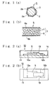
- Fig. 1(a) illustrates the particle of the particulate conductor material according to the present invention in a schematic cross-sectional view.
- Fig. 1(b) illustrates an embodiment of the PTC-element according to the present invention in a schematic longitudinal cross-sectional view.
- Figs. 2(a) and 2(b) show an embodiment of the protective element according to the present invention in a schematic vertical cross-sectional view and in a schematic plan view with exclusion of its cover plate, respectively.
- Figs. 3(a) and 3(b) show an embodiment of the electric circuit board according to the present invention in a plan and in a vertical cross section along the line A-A of the former, respectively.
- Figs. 4(a) and 4(b) show another embodiment of the electric circuit board according to the present invention in a plan and in a vertical cross section along the line B-B of the former, respectively.
- Figs. 5(a) and 5(b) give each a circuit diagram for embodying, as a protective device, the electric circuit board shown in Figs. 3(a), 3(b) or in Figs. 4(a), 4(b), respectively.
- Fig. 6 is a graph representing the experimental results of the inventive Examples and of Comparative Examples.
- any conventional polymer can be used for the crystalline polymer according to the present invention without limitation, as far as they are of organic polymers which are non-conductive and can expand as the temperature increases, wherein preference is given, in particular, to those which can expand abruptly within a narrow temperature range.
- crystalline polymers there may be enumerated, for example, polyolefins, such as polyethylene and polypropylene, and polycaprolactone, wherein the preferred are polyethylene and ethylene/methacrylate copolymers.
- the particulate conductor material according to the present invention may be composed of microspherical particles of an electroconductive substance provided on each particle with irregular surface contours, wherein the shape of the base particle is sphere, preferably perfect sphere, on which micronous irregular contours are formed.
- the particle size may range between 5 and 50 ⁇ m, preferably between 10 and 40 ⁇ m.
- the height of protrusions of such surface irregularity may range between 0.01 and 10 ⁇ m, preferably between 0.1 and 1 ⁇ m, corresponding to the proportion in the range of 1/5 to 1/1,000, preferably 1/10 to 1/100, relative to the particle size.
- the specific weight of the particle may be in the range from 2 to 5, preferably from 2 to 3.5.
- every electroconductive particulate material for example, metals, such as silver and others, carbon and so on.
- a preferred material is particulate carbon, especially particulate graphite or one in which each particle of graphite is coated with a layer of a metal by, for example, plating.
- the metal of the coating layer for example, gold, silver, copper and nickel may be enumerated. Gold is preferable, while a double-layered coating of nickel/gold is more preferable in view of better adhesion on the base particle of carbon.
- the carbon particles having irregular surface contours may be produced by forming on each spherical particle of a particulate thermosetting resin or a carbonized product thereof irregular surface contours by pitch-coating or the like and subjecting the resulting particles to carbonization, while other method may also be employed for producing the carbon particles having irregular surface contours, for example, a method in which each of the spherical carbon particles is coated with a layer of carbon powder.
- a metal layer over the surface of the carbon particle having irregular surface contours physical methods including vacuum deposition ion plating and thermal splaying may be employed, wherein preference is given to plating techniques, such as electrolytic plating and currentless plating.
- plating techniques such as electrolytic plating and currentless plating.
- nickel and gold are preferred.
- the thickness of the metal layer may vary in accordance with each specific technique used, while it may range favorably between 0.02 and 0.2 ⁇ m, in particular, between 0.1 and 0,15 ⁇ m.
- the PTC-element according to the present invention is one in which a kneaded mixture containing the particles of the conductor material dispersed in the matrix consisting of the non-conductive crystalline polymer is arranged between the electrodes.
- the proportion of the particulate conductor material relative to the total mixture may be in the range from 25 to 60 %, preferably from 40 to 50 %, on the volume basis. No satisfactorily low initial value for the volume resistivity can be obtained at a proportion of the particulate conductor material lower than 25 % by volume and, on the other hand, the PTC-element exhibits no satisfactory material properties at a proportion of the particulate conductor material higher than 60 % by volume.
- the PTC-element according to the present invention may contain, in addition to the crystalline non-conductive polymer and the particualte conductor material, other ingredients, such as a heat resistance stabilizer, a weathering stabilizer and so on.
- the PTC-element according to the present invention can be produced by mixing the crystalline non-conductive polymer and the particualte conductor material together with the optionally incorporated additional ingredients, kneading the resulting premix in a molten state and subjecting the kneaded mass to a forming, so as to permit the formed product to be disposed between the electrodes. It is possible to prepare the PTC-element in a form of an integrated unit with the electrodes by press molding the kneaded mass together with two metal foils to be served as the electrodes fitted to the kneaded mass.
- the volume resistivity of the PTC-element according to the present invention obtained in the manner as above does not exceed over 1 ⁇ 10 -1 ⁇ cm before and after the reflowing treatment of solder and such low volume resistivity can be preserved even after repeated tripping thereof. Therefore, the PTC-element according to the present invention is suitable to serve itself for a protective element to be assembled on an electric circuit board which is subjected to a reflowing treatment of the solder, though it finds, of course, general use for protective element for usual purposes.
- the PTC-element according to the present invention has a positive temperature coefficient of electric resistance. At lower temperatures, the particles of the conductor material are held in contact with each other, whereby the electroconductivity of the PTC-element is secured and the volume resistivity thereof is kept low. However, at higher temperatures, especially within a certain specific temperature range, an abrupt expansion of volume of the non-conductive crystalline polymer takes place, whereby the particles of the conductor material become separated from each other, resulting in an abrupt increase in the volume resistivity of the element to thereby cause tripping of the PTC-element and to bring about a current shutoff.
- the PTC-element according to the present invention can, thus, be used as a protective element having a function of detecting any abnormal condition caused from heat evolution in an electric system due to an overcurrent or overvoltage or due to an abnormal electrode reaction in a battery and causing shutoff of current.
- the tripping temperature of the PTC-element according to the present invention can be adjusted in a similar way as in a conventional PTC-element by, for example, selecting each specific non-conductive crystalline polymer and the proportion of the amount of particulate conductor material relative to the non-conductive crystalline polymer.
- the protective device is constructed from the PTC-element mentioned above, a heating element for transmitting a Joule's heat to the PTC-element and a detecting element for detecting any abnormal condition and causing a current to flow through the heating element.
- the heating element is arranged in the protective device according to the present invention in such a manner that the PTC-element and the heating element are held in a thermally joined state under interposition of an electric insulator therebetween.
- One or more PTC-elements may be incorporated in one single protective device.
- the detecting element is arranged to reliably detect any abnormal condition and to cause a current to flow through the heating element when detected.
- a voltage detecting element may be employed by connecting it so as to detect an overvoltage and to cause a current to flow through the heating element when an overvoltage is detected.
- the heating element is actuated upon detection of an abnormal condition, such as an overvoltage, by the detecting element to develop a Joule's heat which is transmitted to the PTC-element to cause tripping thereof, resulting in current shutoff.
- an abnormal condition such as an overvoltage
- the principle of the function of protective device is as above.
- the current shutoff of the PTC-element is actuated by an overvoltage to effect the protecting function.
- the PTC-element or the protective device given above can be mounted on an electric circuit board together with other constituent circuit elements in order to obtain an electric circuit board assembly equipped with the PTC-element or the protective device.
- the PTC-element will not be obstructed by a possible high temperature processing by, such as reflowing of the solder, and the proper function thereof is maintained.
- the electric circuit board according to the present invention is provided with a protective device described above which is composed of the above-mentioned PTC-element, a heating element and a detecting element.
- This electric circuit board can be actuated even in the event of such an abnormal condition as overdischarge or overvoltage other than heat evolution, by detecting it and causing a current to flow through the heating element so as to effect tripping of the PTC-element.
- the PTC-element according to the present invention incorporates microspherical conductive particles with irregular surface contours as the particulate conductor material under dispersion in the matrix of the non-conductive crystalline polymer. It is made possible thereby to obtain a PTC-element having a low volume resistivity at lower temperatrues, a high resistance at the peak and a capability of causing an abrupt increase of the volume resistivity within a narrow temperature range with assurance of a low volume resistivity even after having been subjected to a high temperature heat treatment, such as the reflowing of solder, together with preservation of a low volume resistivity even after repeated trippings thereof.
- a PTC-element exhibiting a low volume resistivity upon current conduction can be obtained.
- a PTC-element exhibiting a low volume resistivity upon current conduction can be obtained in an easy and economic way.
- the protective device comprises the PTC-element(s) described above, the heating element(s) and the detecting element in combination. It functions to protect a current-conducting apparatus or system by detecting an abnormal condition, such as an overvoltage, overcurrent or the like, which is not able to detect by using only the PTC-element.
- an abnormal condition such as an overvoltage, overcurrent or the like
- the initial volume resistivity remains low after having been subjected to a high temperature processing, such as reflowing of solder, and is preserved even after repeated trippings of the PTC-element.
- the volume resistivity of the so-assembled PTC-element(s) will not differ from the initial low value after having been subjected to a high temperature processing by reflowing of the solder upon the assemblage and can be preserved for long term under operation of the circuit with repeated trippings of the PTC-element(s).
- Fig. 1(a) illustrates a typical particle of the particulate conductor material coated with a metal layer according to the present invention in a schematic cross-sectional view.
- Fig. 1(b) shows schematically the PTC-element in a cross-sectional view.
- the particle of the conductor material 1 comprises a microspherical carbon particle 2 having irregular surface contours, which is coated with a metal layer 3.
- the irregular contour of the carbon particle 2 is obtained by providing a layer having irregular protrudings 2b on a base particle 2a of nearly perfect sphere by a pitch-coating with subsequent carbonization.
- the metal layer 3 is plated over the entire surface of the carbon particle 2 by plating first with nickel and then with gold thereon to form a double layered metal coating, though only a single layer is shown in the Drawing.
- the metal layer is shown here in an enlarged thickness for easier view.
- the PTC-element 5 is shown in a construction in which two electrodes 8a ans 8b, each consisting of a metal foil, are attached to both sides of a solid mass 7 composed of a non-conductive matrix of the crystalline polymer 6 and the particulate conductor material 1 dispersed in the matrix.
- the PTC-element 5 is formed as an integrated unit which is produced by kneading the crystalline polymer 6 together with the particulate conductor material 1 into a heterogeneous mixture 7, placing the mixture 7 in between two electrorodes 8a and 8b each consistsing of a metal foil, press-molding the mixture together with the electrodes attached thereto into a molded product and cutting this molded product into the integrated unit of a predetermined size.
- the so-obtained PTC-element 5 can serve for a practical use by inserting it in a detecting or protecting circuit by connecting the electrodes 8a and 8b to the circuit. At lower temperatures, the particles of the particulate conductor material are held in contact with each other to assure electroconductance therethrough, whereas they become separated from each other by expansion of the non-conductive crystalline polymer 6 when heated and the volume resistivity of the PTC-element 5 reaches a high value within a narrow temperature range and, at last, tripping thereof will occur.
- the PTC-element 5 can be used as a detecting element when it is used for observing and displaying the volume resistivity value of the PTC-element, or can be used as a protective element against heat evolution, when it is used for controlling or cutting off the electric current to the heating element.
- the PTC-element 5 can also serve as a detecting or protecting element against occurrence of an overcurrent, since the resistance thereof increases when it is heated by the overcurrent.
- FIGs. 2(a) and 2(b) One enbodiment of the protective device according to the present invention is shown in Figs. 2(a) and 2(b) in a schematic vertical cross-sectional view and in a schematic plan view with removed cover plate, respectively.
- the protective element is indicated by the numeral 10 and the electrodes therefor 12a and 12b are disposed on a substrate board 11.
- the PTC-element 5 is attached to one of the electrodes (12a) so as to connect it to one of the electrodes (8b) of the PTC-element 5, while the other electrode 8a of the PTC-element 5 is connected with the other electrode 12b of the protective element 10 on the board 11 by a metal foil 13 bridging therebetween.
- the entire protective element is covered by a cap 14.
- the substrate board 11 is made of an insulating material, for example, a glass fiber-reinforced epoxy resin, on which the electrodes 12a and 12b, each made of, for example, a metal foil of copper or the like, are disposed.
- the electrodes 8a and 8b of the PTC-element 5, the electrodes 12a and 12b of the protective element 10 and the metal foil 13 are mounted by reflowing of solder.
- the protective element 10 may be disposed close to the heating element for transmitting heat to the PTC-element in order to attain tripping of the PTC-element due to increase in the volume resistivity thereof by being heated by the transmitted heat to cause current shutoff, whereby the current conducting apparatus or system provided with the protective device according to the present invention can reliable be protected.
- FIGs. 3(a) and 3(b) an embodiment of the electric circuit board according to the present invention is shown in a schematic plan view and in a schematic vertical cross-sectional view along the line A-A of the former, respectively.
- the electrodes 12a and 12b for the PTC-elements and the electrodes 15a and 15b for the heating element 16 are arranged on the substrate board 11 as patterned conductor segments.
- the electrodes 12a and 12b for PTC-elements are connected to the PTC-elements 5a and 5b and a metal foil 13 is disposed to connect the PTC-elements by bridging between them, so as to build up the protective element.
- a heating element 16 is arranged between the PTC-elements 5a and 5b so as to hold an electric connection with the electrodes 15a and 15b for the heating element but is insulated from other elements by being surrounded by an insulators 17.
- the entire protective element is covered by a cap or sealing member 14.
- the electrodes 12a and 12b, the PTC-elements 5a and 5b and the metal foil 13 in the electric circuit board 20 are interconnected with solder by reflowing of the solder.
- the PTC-elements 5a and 5b are brought to tripping when the heating element 16 becomes heated, whereby the current through the electrodes 12a and 12b becomes reduced.
- Fig. 4(a) shows an alternative embodiment of the electric circuit board according to the present invention in a schematic plan view.
- Fig. 4(b) shows the embodiment of Fig. 4(a) in a schematic vertical cross-sectional view along the line B-B of the former.
- an intermediate electrode 12c is disposed between the electrodes 12a and 12b for the PTC-elements in such a manner that the heating elements 16a and 16b are arranged separately so as to connect the intermediate electrode 12c with the electrode 12a or with the electrode 12b, respectively, wherein the PTC-element 5a and the PTC-element 5b are interconnected by a metal foil 13 via the intermediate electrode 12c.
- the electrodes 12a, 12b and 12c, the PTC-elements 5a and 5b and the metal foil 13 in the above electric circuit board 20 are interconnected with solder by reflowing of the solder.
- the PTC-elements 5a and 5b are brought to tripping when the heating elements 16a and 16b become heated, whereby the current through the electrodes 12a and 12b becomes reduced, so that a protection of a current conducting apparatus or system employing this circuit board assembly can be attained by the reduction of heat evolution in the heating elements 16a and 16b due to the so-decreased current through the electrodes 15a and 15b.
- Figs. 5(a) shows a circuit diagram embodying the electric circuit board shown in Figs. 3(a) and 3(b) as the protective device according to the present invention.
- This protective device comprises PTC-elements 5a and 5b, a heating element 16 and a detecting element 21.
- the PTC-elements 5a and 5b, the heating element 16 and a transistor 22 of the detecting element 21 are connected in series between the terminals f and g, wherein a Zener diode 23 and a resistor 24 which constitute the detecting element 21 are interposed between the terminal f and the base of the transistor 22.
- Each of the constituent members of the detecting element 21 assembled in this electric circuit board 20 is not shown in Figs. 3(a) and 3(b).
- the protective device of this embodiment can be used for protecting against an overvoltage in, for example, a charging circuit of a storage battery or the like.
- Fig. 5(b) shows a circuit diagram embodying the electric circuit board shown in Figs. 4(a) and 4(b) as a protective device according to the present invention.
- This protective device comprises PTC-elements 5a and 5b, heating elements 16a and 16b and a detecting element 21.
- wiring is realized in the same manner as that in Fig. 5(a), except that the PTC-elements 5a and 5b and the heating elements 16a and 16b are arranged under separation by an intermediate electrode 12c.
- the detecting element 21 will be actuated when an overvoltage occurs both in the case where the current conduction occurs on the side of the terminals f and g and in the case where the current conduction is effected through the terminals h and i, to thereby cause both the heating elements 16a and 16b to be heated by the Joule's heat, whereby both the PTC-elements are brought to tripping and to effect shutoff of the current to the heating elements 16a and 16b.
- the protective device of this embodiment can thus be utelized in, for example, a charging circuit of a storage battery for protecting against overvoltage.
- Each a particulate conductor material (Conductor 1 or Conductor 2) was prepared by processing a product of microspherical carbon particles of spherical particle form ⁇ CARBON MICROBEADS PC (trademark), a product of Nippon Carbon K.K. ⁇ by providing on each particle with surface irregularities by means of pitch-coating (Examples 1 and 2), onto which a metal coating layer was applied by a currentless plating first with nickel and then with gold thereon.
- HDPE high dencity polyethylene product
- EOA ethylene/ethyl acrylate copolymer
- NUC 6170 product of Nippon Unicar Co., Ltd.
- Each of the particulate conductor materials prepared as above and the above non-conductive crystalline polymer were blended in a proportion as given in Table 1 by kneading on a press kneader at 190 °C and the resulting mass was press-molded on a hot press under a condition of 190°C, 0.49 MPa (5 kgf/cm 2 ) for 20 sec. into a film having a thickness of 300 ⁇ m. This film was placed between two nickel foils and the resulting lamination was further processed by a hot press (190 °C, 0.49 MPa, for 30 sec.) into a PTC-element having a thickness of 200 ⁇ m.
- the increase in the electric resistance is lower for the inventive Examples 1 and 2 in which particulate conductor particles having surface irregularyties are used, as compared with the Comparative Examples 1 and 2.
- the increase in the resistance was found to be low in particular for Example 2 in which a particulate conductor material with a particle size of 10 ⁇ m was employed.
Abstract
Description
- The present invention relates to a Positive Temperature Coefficient element (hereafter abbreviated as PTC-element) having a positive temperature coefficient of electric resistance, especially a PTC-element usable as a protective device for protecting against overcurrent, overvoltage and other phenomena involving heat evolution; as well as to a protective device and electric circuit board using such PTC-element.
- A PTC-element, also called a PTC-thermistor, has a positive temperature coefficient of electric resistance, wherein the electric resistance thereof increases as the temperature is elevated, and is used as a protective device for protecting against overcurrent, overvoltage and other phenomena involving heat evolution. Currently used PTC-element is composed of a matrix of a non-conductive crystalline polymer and of, dispersed therein, an electroconductive particulate material. The electric resistance of such a PTC-element is low at lower temperatures since the particles of the conductor material are held in contact with each other at lower temperatures. However, when the temperature is elevated, the electric resistance becomes increased by a possible occurrence of separation of the particles of the conductor from their contact due to thermal expansion of the non-conductive crystalline polymer and reaches finally a current shutoff.
- As PTC-elements of prior art, there have been proposed, for example, those in which spherical carbon particles, in particular, of perfect sphere are used for the conductor material (Japanese Patent Application Laid-open Hei-8-298201 A) and those in which such spherical carbon particles as above are provided each with a surface coating layer of metal (Japanese Patent Application Laid-open Hei-8-172001 A).
- Such PTC-elements using a spherical particulate conductor material are said to have a low volume resistivity, a high electric resistance at the peak and a capability of steep increase in the resistance within a narrow range of temperature.
- Upon mounting such a conventional PTC-element on the surface of an electric circuit board, however, a problem is brought about, in which the initial volume resistivity of the PTC-element is, in some cases, set at a high value due to a possible temperature elevation upon the assemblage thereof, when a high temperature processing, such as reflowing treatment of the solder, is employed, whereby its use as an assembled PTC-element becomes difficult.
- An object of the present invention is to provide a PTC-element having a low volume resistivity, a high electric resistance at the peak, a capability of an abrupt elevation of the electric resistance within a narrow temperature range, a low initial value of the volume resistivity even after having been subjected to a high temperature processing, such as reflowing treatment of solder, and a capability of preserving the low volume resistivity after repeated trippings.
- Another object of the present invention is to provide a protective device using the PTC-element mentioned above.
- A further object of the present invention is to provide an electric circuit board equipped with such a protective device as mentioned above.
- The PTC-element according to the present invention comprises a non-conductive crystalline polymer and a particulate conductor material dispersed in the non-conductive crystalline polymer, wherein the conductor material comprises electroconductive particles having irregular surface contours.
- The protective device according to the present invention comprises
- a PTC-element comprising a non-conductive crystalline polymer and a particulate conductor material dispersed in the non-conductive crystalline polymer, wherein the conductor material comprises electroconductive particles having irregular surface contours,
- a heating element for transmitting heat to the PTC-element and
- a detecting element for detecting any abnormal condition and flowing a current through the heating element when detected.
-
- The electric circuit board according to the present invention comprises, installed therein, a protective device which comprises
- a PTC-element comprising a non-conductive crystalline polymer and a particulate conductor material dispersed in the non-conductive crystalline polymer, wherein the conductor material comprises electroconductive particles having irregular surface contours,
- a heating element for transmitting heat to the PTC-element and
- a detecting element for detecting any abnormal condition and flowing a current through the heating element when detected.
-
- Fig. 1(a) illustrates the particle of the particulate conductor material according to the present invention in a schematic cross-sectional view.
- Fig. 1(b) illustrates an embodiment of the PTC-element according to the present invention in a schematic longitudinal cross-sectional view.
- Figs. 2(a) and 2(b) show an embodiment of the protective element according to the present invention in a schematic vertical cross-sectional view and in a schematic plan view with exclusion of its cover plate, respectively.
- Figs. 3(a) and 3(b) show an embodiment of the electric circuit board according to the present invention in a plan and in a vertical cross section along the line A-A of the former, respectively.
- Figs. 4(a) and 4(b) show another embodiment of the electric circuit board according to the present invention in a plan and in a vertical cross section along the line B-B of the former, respectively.
- Figs. 5(a) and 5(b) give each a circuit diagram for embodying, as a protective device, the electric circuit board shown in Figs. 3(a), 3(b) or in Figs. 4(a), 4(b), respectively.
- Fig. 6 is a graph representing the experimental results of the inventive Examples and of Comparative Examples.
- Any conventional polymer can be used for the crystalline polymer according to the present invention without limitation, as far as they are of organic polymers which are non-conductive and can expand as the temperature increases, wherein preference is given, in particular, to those which can expand abruptly within a narrow temperature range. For such crystalline polymers, there may be enumerated, for example, polyolefins, such as polyethylene and polypropylene, and polycaprolactone, wherein the preferred are polyethylene and ethylene/methacrylate copolymers.
- The particulate conductor material according to the present invention may be composed of microspherical particles of an electroconductive substance provided on each particle with irregular surface contours, wherein the shape of the base particle is sphere, preferably perfect sphere, on which micronous irregular contours are formed. The particle size may range between 5 and 50 µm, preferably between 10 and 40 µm. The height of protrusions of such surface irregularity may range between 0.01 and 10 µm, preferably between 0.1 and 1 µm, corresponding to the proportion in the range of 1/5 to 1/1,000, preferably 1/10 to 1/100, relative to the particle size. The specific weight of the particle may be in the range from 2 to 5, preferably from 2 to 3.5.
- It is permissible to use for such a conductor material, without any special limitation, every electroconductive particulate material, for example, metals, such as silver and others, carbon and so on. From the view point of facilitated production and so on, a preferred material is particulate carbon, especially particulate graphite or one in which each particle of graphite is coated with a layer of a metal by, for example, plating. For the metal of the coating layer, for example, gold, silver, copper and nickel may be enumerated. Gold is preferable, while a double-layered coating of nickel/gold is more preferable in view of better adhesion on the base particle of carbon.
- The carbon particles having irregular surface contours may be produced by forming on each spherical particle of a particulate thermosetting resin or a carbonized product thereof irregular surface contours by pitch-coating or the like and subjecting the resulting particles to carbonization, while other method may also be employed for producing the carbon particles having irregular surface contours, for example, a method in which each of the spherical carbon particles is coated with a layer of carbon powder.
- For forming a metal layer over the surface of the carbon particle having irregular surface contours, physical methods including vacuum deposition ion plating and thermal splaying may be employed, wherein preference is given to plating techniques, such as electrolytic plating and currentless plating. For the material to be plated, nickel and gold are preferred. The thickness of the metal layer may vary in accordance with each specific technique used, while it may range favorably between 0.02 and 0.2 µm, in particular, between 0.1 and 0,15 µm.
- The PTC-element according to the present invention is one in which a kneaded mixture containing the particles of the conductor material dispersed in the matrix consisting of the non-conductive crystalline polymer is arranged between the electrodes. The proportion of the particulate conductor material relative to the total mixture may be in the range from 25 to 60 %, preferably from 40 to 50 %, on the volume basis. No satisfactorily low initial value for the volume resistivity can be obtained at a proportion of the particulate conductor material lower than 25 % by volume and, on the other hand, the PTC-element exhibits no satisfactory material properties at a proportion of the particulate conductor material higher than 60 % by volume.
- The PTC-element according to the present invention may contain, in addition to the crystalline non-conductive polymer and the particualte conductor material, other ingredients, such as a heat resistance stabilizer, a weathering stabilizer and so on.
- The PTC-element according to the present invention can be produced by mixing the crystalline non-conductive polymer and the particualte conductor material together with the optionally incorporated additional ingredients, kneading the resulting premix in a molten state and subjecting the kneaded mass to a forming, so as to permit the formed product to be disposed between the electrodes. It is possible to prepare the PTC-element in a form of an integrated unit with the electrodes by press molding the kneaded mass together with two metal foils to be served as the electrodes fitted to the kneaded mass.
- The volume resistivity of the PTC-element according to the present invention obtained in the manner as above does not exceed over 1 × 10⁻¹ Ω cm before and after the reflowing treatment of solder and such low volume resistivity can be preserved even after repeated tripping thereof. Therefore, the PTC-element according to the present invention is suitable to serve itself for a protective element to be assembled on an electric circuit board which is subjected to a reflowing treatment of the solder, though it finds, of course, general use for protective element for usual purposes.
- The PTC-element according to the present invention has a positive temperature coefficient of electric resistance. At lower temperatures, the particles of the conductor material are held in contact with each other, whereby the electroconductivity of the PTC-element is secured and the volume resistivity thereof is kept low. However, at higher temperatures, especially within a certain specific temperature range, an abrupt expansion of volume of the non-conductive crystalline polymer takes place, whereby the particles of the conductor material become separated from each other, resulting in an abrupt increase in the volume resistivity of the element to thereby cause tripping of the PTC-element and to bring about a current shutoff.
- The PTC-element according to the present invention can, thus, be used as a protective element having a function of detecting any abnormal condition caused from heat evolution in an electric system due to an overcurrent or overvoltage or due to an abnormal electrode reaction in a battery and causing shutoff of current.
- The tripping temperature of the PTC-element according to the present invention can be adjusted in a similar way as in a conventional PTC-element by, for example, selecting each specific non-conductive crystalline polymer and the proportion of the amount of particulate conductor material relative to the non-conductive crystalline polymer.
- The protective device according to the present invention is constructed from the PTC-element mentioned above, a heating element for transmitting a Joule's heat to the PTC-element and a detecting element for detecting any abnormal condition and causing a current to flow through the heating element. The heating element is arranged in the protective device according to the present invention in such a manner that the PTC-element and the heating element are held in a thermally joined state under interposition of an electric insulator therebetween. One or more PTC-elements may be incorporated in one single protective device. The detecting element is arranged to reliably detect any abnormal condition and to cause a current to flow through the heating element when detected. As the detecting element, for example, a voltage detecting element may be employed by connecting it so as to detect an overvoltage and to cause a current to flow through the heating element when an overvoltage is detected.
- In the above-mentioned protective device, the heating element is actuated upon detection of an abnormal condition, such as an overvoltage, by the detecting element to develop a Joule's heat which is transmitted to the PTC-element to cause tripping thereof, resulting in current shutoff. The principle of the function of protective device is as above. In a protective device using a detecting element based on detection of an overvoltage, the current shutoff of the PTC-element is actuated by an overvoltage to effect the protecting function.
- The PTC-element or the protective device given above can be mounted on an electric circuit board together with other constituent circuit elements in order to obtain an electric circuit board assembly equipped with the PTC-element or the protective device. Here, the PTC-element will not be obstructed by a possible high temperature processing by, such as reflowing of the solder, and the proper function thereof is maintained.
- The electric circuit board according to the present invention is provided with a protective device described above which is composed of the above-mentioned PTC-element, a heating element and a detecting element. This electric circuit board can be actuated even in the event of such an abnormal condition as overdischarge or overvoltage other than heat evolution, by detecting it and causing a current to flow through the heating element so as to effect tripping of the PTC-element. For instance, when an overvoltage appears in the charging circuit of a storage battery at the end of the charging operation or when an overdischarge appears in the output line of a battery or cell due to an abnormal electrode reaction, it is detected by the detecting element which causes the heating element to actuate, whereby tripping of the PTC-element is brought about.
- As described above, the PTC-element according to the present invention incorporates microspherical conductive particles with irregular surface contours as the particulate conductor material under dispersion in the matrix of the non-conductive crystalline polymer. It is made possible thereby to obtain a PTC-element having a low volume resistivity at lower temperatrues, a high resistance at the peak and a capability of causing an abrupt increase of the volume resistivity within a narrow temperature range with assurance of a low volume resistivity even after having been subjected to a high temperature heat treatment, such as the reflowing of solder, together with preservation of a low volume resistivity even after repeated trippings thereof.
- It is easy to fabricate a PTC-element having a low initial volume resistivity, when carbon particles having irregular surface contours are employed for the above-mentioned microspherical particles with irregular surface contours. Appropriate irregular surface contours may be attained by, in particular, using carbon particles each having surface irregularities obtained by pitch-coating on the basal carbon particles.
- When a particulate conductor material provided on the surface of each particle with a metal layer is employed, a PTC-element exhibiting a low volume resistivity upon current conduction can be obtained. When a particulate conductor material obtained by coating carbon particles each having irregular surface contours with a metal layer is employed, a PTC-element exhibiting a low volume resistivity upon current conduction can be obtained in an easy and economic way.
- The protective device according to the present invention comprises the PTC-element(s) described above, the heating element(s) and the detecting element in combination. It functions to protect a current-conducting apparatus or system by detecting an abnormal condition, such as an overvoltage, overcurrent or the like, which is not able to detect by using only the PTC-element. Here also, the initial volume resistivity remains low after having been subjected to a high temperature processing, such as reflowing of solder, and is preserved even after repeated trippings of the PTC-element.
- Since the electric circuit board according to the present invention is provided with the above-described PTC-element(s) or protective device, the volume resistivity of the so-assembled PTC-element(s) will not differ from the initial low value after having been subjected to a high temperature processing by reflowing of the solder upon the assemblage and can be preserved for long term under operation of the circuit with repeated trippings of the PTC-element(s).
- Below, the present invention will further be described in more detail by way of embodiments thereof with reference to the appended Drawings.
- Fig. 1(a) illustrates a typical particle of the particulate conductor material coated with a metal layer according to the present invention in a schematic cross-sectional view. Fig. 1(b) shows schematically the PTC-element in a cross-sectional view.
- As shown in Fig. 1(a), the particle of the conductor material 1 comprises a
microspherical carbon particle 2 having irregular surface contours, which is coated with a metal layer 3. The irregular contour of thecarbon particle 2 is obtained by providing a layer havingirregular protrudings 2b on abase particle 2a of nearly perfect sphere by a pitch-coating with subsequent carbonization. The metal layer 3 is plated over the entire surface of thecarbon particle 2 by plating first with nickel and then with gold thereon to form a double layered metal coating, though only a single layer is shown in the Drawing. The metal layer is shown here in an enlarged thickness for easier view. - In Fig. 1(b), the PTC-
element 5 is shown in a construction in which twoelectrodes 8a ans 8b, each consisting of a metal foil, are attached to both sides of asolid mass 7 composed of a non-conductive matrix of thecrystalline polymer 6 and the particulate conductor material 1 dispersed in the matrix. - The PTC-
element 5 is formed as an integrated unit which is produced by kneading thecrystalline polymer 6 together with the particulate conductor material 1 into aheterogeneous mixture 7, placing themixture 7 in between twoelectrorodes - The so-obtained PTC-
element 5 can serve for a practical use by inserting it in a detecting or protecting circuit by connecting theelectrodes crystalline polymer 6 when heated and the volume resistivity of the PTC-element 5 reaches a high value within a narrow temperature range and, at last, tripping thereof will occur. - The PTC-
element 5 can be used as a detecting element when it is used for observing and displaying the volume resistivity value of the PTC-element, or can be used as a protective element against heat evolution, when it is used for controlling or cutting off the electric current to the heating element. The PTC-element 5 can also serve as a detecting or protecting element against occurrence of an overcurrent, since the resistance thereof increases when it is heated by the overcurrent. - One enbodiment of the protective device according to the present invention is shown in Figs. 2(a) and 2(b) in a schematic vertical cross-sectional view and in a schematic plan view with removed cover plate, respectively.
- In Figs. 2(a) and 2(b), the protective element is indicated by the numeral 10 and the electrodes therefor 12a and 12b are disposed on a
substrate board 11. The PTC-element 5 is attached to one of the electrodes (12a) so as to connect it to one of the electrodes (8b) of the PTC-element 5, while theother electrode 8a of the PTC-element 5 is connected with theother electrode 12b of theprotective element 10 on theboard 11 by ametal foil 13 bridging therebetween. The entire protective element is covered by acap 14. - The
substrate board 11 is made of an insulating material, for example, a glass fiber-reinforced epoxy resin, on which theelectrodes electrodes element 5, theelectrodes protective element 10 and themetal foil 13 are mounted by reflowing of solder. - The
protective element 10 may be disposed close to the heating element for transmitting heat to the PTC-element in order to attain tripping of the PTC-element due to increase in the volume resistivity thereof by being heated by the transmitted heat to cause current shutoff, whereby the current conducting apparatus or system provided with the protective device according to the present invention can reliable be protected. - In Figs. 3(a) and 3(b), an embodiment of the electric circuit board according to the present invention is shown in a schematic plan view and in a schematic vertical cross-sectional view along the line A-A of the former, respectively.
- In the
electric circuit board 20, theelectrodes electrodes heating element 16 are arranged on thesubstrate board 11 as patterned conductor segments. Theelectrodes elements metal foil 13 is disposed to connect the PTC-elements by bridging between them, so as to build up the protective element. Aheating element 16 is arranged between the PTC-elements electrodes insulators 17. The entire protective element is covered by a cap or sealingmember 14. - The
electrodes elements metal foil 13 in theelectric circuit board 20 are interconnected with solder by reflowing of the solder. - In the
electric circuit board 20, the PTC-elements heating element 16 becomes heated, whereby the current through theelectrodes - Fig. 4(a) shows an alternative embodiment of the electric circuit board according to the present invention in a schematic plan view. Fig. 4(b) shows the embodiment of Fig. 4(a) in a schematic vertical cross-sectional view along the line B-B of the former. In this embodiment, an
intermediate electrode 12c is disposed between theelectrodes heating elements intermediate electrode 12c with theelectrode 12a or with theelectrode 12b, respectively, wherein the PTC-element 5a and the PTC-element 5b are interconnected by ametal foil 13 via theintermediate electrode 12c. - The
electrodes elements metal foil 13 in the aboveelectric circuit board 20 are interconnected with solder by reflowing of the solder. - In the above
electric circuit board 20, the PTC-elements heating elements electrodes heating elements electrodes - Figs. 5(a) shows a circuit diagram embodying the electric circuit board shown in Figs. 3(a) and 3(b) as the protective device according to the present invention. This protective device comprises PTC-
elements heating element 16 and a detectingelement 21. In the arrangement of Fig. 5(a), the PTC-elements heating element 16 and atransistor 22 of the detectingelement 21 are connected in series between the terminals f and g, wherein aZener diode 23 and aresistor 24 which constitute the detectingelement 21 are interposed between the terminal f and the base of thetransistor 22. Each of the constituent members of the detectingelement 21 assembled in thiselectric circuit board 20 is not shown in Figs. 3(a) and 3(b). - In the above protective device, a current begins to flow through the
Zener diode 23 when an overvoltage imposed between the terminals f and g reaches the Zener voltage, whereby thetransistor 22 is actuated to pass a current therethrough and through theheating element 16 to cause heat evolution. This Joule's heat is transmitted to the PTC-elements metal foil 13 and causes an increase in the resistance thereof to effect at last tripping thereof to reach a current shutoff. Thus, the protective device of this embodiment can be used for protecting against an overvoltage in, for example, a charging circuit of a storage battery or the like. - Fig. 5(b) shows a circuit diagram embodying the electric circuit board shown in Figs. 4(a) and 4(b) as a protective device according to the present invention. This protective device comprises PTC-
elements heating elements element 21. In this embodiment, wiring is realized in the same manner as that in Fig. 5(a), except that the PTC-elements heating elements intermediate electrode 12c. - In this protective device, the detecting
element 21 will be actuated when an overvoltage occurs both in the case where the current conduction occurs on the side of the terminals f and g and in the case where the current conduction is effected through the terminals h and i, to thereby cause both theheating elements heating elements - Below, the present invention will further be described in more detail by way of Examples.
- Each a particulate conductor material (Conductor 1 or Conductor 2) was prepared by processing a product of microspherical carbon particles of spherical particle form {CARBON MICROBEADS PC (trademark), a product of Nippon Carbon K.K.} by providing on each particle with surface irregularities by means of pitch-coating (Examples 1 and 2), onto which a metal coating layer was applied by a currentless plating first with nickel and then with gold thereon. In Comparative Examples 1 and 2, the same procedures were pursued except that a product of microspherical carbon particles of particle form of perfect sphere {CARBON MICROBEADS ICB (trademark), a product of Nippon Carbon K.K.} was employed to obtain the particulate conductor material (Conductor 3 and
Conductor 4, respectively). - Conductor 1 a carbon product having a particle size of 5 µm with surface protrusions of average height of 0.5 µm processed by pitch-coating and carbonization with subsequent metal plating of Ni/Au with Ni thickness of 0.092 µm and Au thickness of 0.061 µm.
-
Conductor 2 a carbon product having a particle size of 10 µm with surface protrusions of average height of 1.0 µm processed by pitch-coating with subsequent metal plating of Ni/Au with Ni thickness of 0.110 µm and Au thickness of 0.064 µm. - Conductor 3 a carbon product having a particle size of 5 µm of a particle form of perfect sphere processed by metal plating of Ni/Au with Ni thickness of 0.091 µm and Au thickness of 0.061 µm.
- Conductor 4 a carbon product having a particle size of 10 µm of a particle form of perfect sphere processed by metal plating of Ni/Au with Ni thickness of 0.110 µm and Au thickness of 0.057 µm.
-
- A high dencity polyethylene product (HDPE) (HIZEX 5000H (trademark), a product of Mitsui Petrochemical Ind., Ltd.) and an ethylene/ethyl acrylate copolymer (EEA) (NUC 6170 (trademark), a product of Nippon Unicar Co., Ltd.) were used for the non-conductive crystalline polymer. Each of the particulate conductor materials prepared as above and the above non-conductive crystalline polymer were blended in a proportion as given in Table 1 by kneading on a press kneader at 190 °C and the resulting mass was press-molded on a hot press under a condition of 190°C, 0.49 MPa (5 kgf/cm2) for 20 sec. into a film having a thickness of 300µm. This film was placed between two nickel foils and the resulting lamination was further processed by a hot press (190 °C, 0.49 MPa, for 30 sec.) into a PTC-element having a thickness of 200 µm.
- The initial volume reisistivity of this PTC-element was observed. Using this PTC-element, a protective device was prepared by mounting it on a substrate board in a manner similar to that shown in Fig. 2 by incorporating a reflowing treatment of solder at a reflowing temperature of 250 °C. The resulting protective device was examined for its volume resistivity after being subjected to the reflowing treatment, for the electric resistance upon conduction of a overcurrent (10 A) and for the electric resistance after repeating 100 cycles of current conduction at a current of 10 A. The results are summarized in Table 1.
Example Compar. Example 1 2 1 2 Composition in Vol. % Polyethylene 34 34 34 34 Etylene/MMA 18 18 18 18 copolymer Conductor 1 48 - - - Conductor 2 - 48 - - Conductor 3 - - 48 - Conductor 4 - - - 48 Resistance (Ω cm X 10-2) Before reflow. 5.5 4.3 4.9 5.5 After reflow. 7.2 5.9 20 13 Overcurr. test On conduction 10 A (Ω cm) 3.0 x10 3.0 x10 2.9 x10 3.3 x10 After 100 cyc. (On 6 sec. Off 54 sec.) 10 A (Ω cm) 2.0x10⁻¹ 8.0x10⁻² 6.0x10⁻¹ 2.0x10⁻¹ - From Table 1, it is seen that both observed values of resistance before and after reflowing are lower (both at values below 1 × 10⁻¹) for the inventive Examples 1 and 2, as compared with those of Comparative Examples 1 and 2. Concerning the volume resistivity after 100 cycles of on-off tests, both the inventive Examples 1 and 2 resulted in lower values than those of Comparativ Examples 1 and 2, wherein, in particular, the volume resistivity for Example 2 in which a particulate conductor material having a particle size of 10 µm was employed gave lower value.
- The above PTC-elements were mounted on a substrate board in a similar manner as shown in Figs. 3(a) and 3(b) and the resulting circuit board was installed in an electric circuit in a similar manner as shown in Fig. 5(a) to prepare a protective device. Using this protective device, an on-off repeating test was carried out by imposing a voltage of 4.5 volts between the terminals of f and g with 5 minutes of "on" and 5 minutes of "off", the results of which are recited in Fig. 6 as a graphic illustration.
- As seen in Fig. 6, the increase in the electric resistance is lower for the inventive Examples 1 and 2 in which particulate conductor particles having surface irregularyties are used, as compared with the Comparative Examples 1 and 2. The increase in the resistance was found to be low in particular for Example 2 in which a particulate conductor material with a particle size of 10 µm was employed.
Claims (11)
- A PTC-element comprising a non-conductive crystalline polymer and a particulate conductor material dispersed in the non-conductive crystalline polymer, wherein the conductor material comprises electroconductive particles having irregular surface contours.
- A PTC-element as claimed in Claim 1, wherein the conductor material comprises microspherical carbon particles having irregular surface contours.
- A PTC-element as claimed in Claim 1, wherein the conductor material comprises microspherical carbon particles having surface irregularity formed by surface coating.
- A PTC-element as claimed in any one of Claims 1 to 3, wherein the conductor material comprises electroconductive particles having a surface coating metal layer.
- A PTC-element as claimed in Claim 4, wherein the volume resistivity of the PTC-element before and after a reflowing treatment does not exceed over a value of 1 × 10⁻¹ Ω · cm.
- A protective device comprisinga PTC-element comprising a non-conductive crystalline polymer and a particulate conductor material dispersed in the non-conductive crystalline polymer, wherein the conductor material comprises electroconductive particles having irregular surface contours,a heating element for transmitting heat to the PTC-element anda detecting element for detecting any abnormal condition and flowing a current through the heating element when detected.
- A protective device as claimed in Claim 6, wherein a plurality of the PTC-elements are provided.
- A protective device as claimed in Claim 6 or 7, wherein the detecting element is a voltage detecting element.
- A protective device as claimed in any one of Claims 6 to 8, wherein the FTC-element and the heating element are held in a thermally joined state under interposition of an electric insulator.
- An electric circuit board comprising, installed therein, a PTC-element comprising a non-conductive crystalline polymer and a particulate conductor material dispersed in the non-conductive crystalline polymer, wherein the conductor material comprises electroconductive particles having irregular surface contours.
- An electric circuit board comprising, installed therein, a protective device which comprisesa PTC-element comprising a non-conductive crystalline polymer and a particulate conductor material dispersed in the non-conductive crystalline polymer, wherein the conductor material comprises electroconductive particles having irregular surface contours,a heating element for transmitting heat to the FTC-element anda detecting element for detecting any abnormal condition and flowing a current through the heating element when detected.
Applications Claiming Priority (3)
| Application Number | Priority Date | Filing Date | Title |
|---|---|---|---|
| JP27465797 | 1997-10-07 | ||
| JP274657/97 | 1997-10-07 | ||
| JP27465797 | 1997-10-07 |
Publications (3)
| Publication Number | Publication Date |
|---|---|
| EP0908902A2 true EP0908902A2 (en) | 1999-04-14 |
| EP0908902A3 EP0908902A3 (en) | 1999-09-22 |
| EP0908902B1 EP0908902B1 (en) | 2006-04-19 |
Family
ID=17544751
Family Applications (1)
| Application Number | Title | Priority Date | Filing Date |
|---|---|---|---|
| EP98308088A Expired - Lifetime EP0908902B1 (en) | 1997-10-07 | 1998-10-05 | PTC-element, protective device and electric circuit board |
Country Status (5)
| Country | Link |
|---|---|
| US (1) | US6114672A (en) |
| EP (1) | EP0908902B1 (en) |
| JP (1) | JP3257521B2 (en) |
| KR (1) | KR100551099B1 (en) |
| DE (1) | DE69834231T2 (en) |
Cited By (4)
| Publication number | Priority date | Publication date | Assignee | Title |
|---|---|---|---|---|
| EP1047092A2 (en) * | 1999-04-23 | 2000-10-25 | Sony Chemicals Corporation | Overcurrent protection device |
| EP1156527A2 (en) * | 2000-05-17 | 2001-11-21 | Sony Chemicals Corporation | Protective fuse element |
| WO2002063739A1 (en) * | 2001-02-06 | 2002-08-15 | Sony Chemicals Corp. | Protection circuit-equipped secondary battery |
| EP1577906A2 (en) * | 2004-03-20 | 2005-09-21 | Wilhelm Pudenz GmbH | Fuse with an element increasing its electrical resistance on rising temperature |
Families Citing this family (37)
| Publication number | Priority date | Publication date | Assignee | Title |
|---|---|---|---|---|
| AU6531600A (en) | 1999-08-27 | 2001-03-26 | Lex Kosowsky | Current carrying structure using voltage switchable dielectric material |
| US6606228B1 (en) * | 2000-11-27 | 2003-08-12 | Ametek, Inc. | Fault detection circuit for use with a power control device |
| TW487272U (en) * | 2001-03-20 | 2002-05-11 | Polytronics Technology Corp | Multilayer circuit boards |
| US6462317B1 (en) * | 2001-05-03 | 2002-10-08 | Hewlett-Packard Company | Heater bar utilizing a positive temperature coefficient heating element |
| KR100411778B1 (en) * | 2001-10-12 | 2003-12-24 | 주식회사 쎄라텍 | Manufacturing method for positive temperature coefficent thermistor |
| JP2004214033A (en) * | 2002-12-27 | 2004-07-29 | Sony Chem Corp | Protection element |
| US20060176675A1 (en) * | 2003-03-14 | 2006-08-10 | Bourns, Inc. | Multi-layer polymeric electronic device and method of manufacturing same |
| JP2005038974A (en) * | 2003-07-18 | 2005-02-10 | Nec Tokin Corp | Macromolecular ptc element and its manufacturing method |
| DE102004016619A1 (en) * | 2004-04-03 | 2005-10-13 | Daimlerchrysler Ag | Electrical component |
| KR100622598B1 (en) * | 2004-12-08 | 2006-09-19 | 엘에스전선 주식회사 | Anisotropic conductive adhesive having ptc characteristic |
| EP1969627A4 (en) | 2005-11-22 | 2010-01-20 | Shocking Technologies Inc | Semiconductor devices including voltage switchable materials for over-voltage protection |
| US20080029405A1 (en) * | 2006-07-29 | 2008-02-07 | Lex Kosowsky | Voltage switchable dielectric material having conductive or semi-conductive organic material |
| US7981325B2 (en) | 2006-07-29 | 2011-07-19 | Shocking Technologies, Inc. | Electronic device for voltage switchable dielectric material having high aspect ratio particles |
| CN101536190A (en) | 2006-09-24 | 2009-09-16 | 肖克科技有限公司 | Formulations for voltage switchable dielectric material having a stepped voltage response and methods for making the same |
| EP2067145A2 (en) * | 2006-09-24 | 2009-06-10 | Shocking Technologies, Inc. | Technique for plating substrate devices using voltage switchable dielectric material and light assistance |
| US20090050856A1 (en) * | 2007-08-20 | 2009-02-26 | Lex Kosowsky | Voltage switchable dielectric material incorporating modified high aspect ratio particles |
| US8206614B2 (en) * | 2008-01-18 | 2012-06-26 | Shocking Technologies, Inc. | Voltage switchable dielectric material having bonded particle constituents |
| US20090220771A1 (en) * | 2008-02-12 | 2009-09-03 | Robert Fleming | Voltage switchable dielectric material with superior physical properties for structural applications |
| US7973533B2 (en) | 2008-02-27 | 2011-07-05 | Vertical Power, Inc. | In-circuit testing for integrity of solid-state switches |
| US9208931B2 (en) | 2008-09-30 | 2015-12-08 | Littelfuse, Inc. | Voltage switchable dielectric material containing conductor-on-conductor core shelled particles |
| WO2010039902A2 (en) | 2008-09-30 | 2010-04-08 | Shocking Technologies, Inc. | Voltage switchable dielectric material containing conductive core shelled particles |
| US8272123B2 (en) | 2009-01-27 | 2012-09-25 | Shocking Technologies, Inc. | Substrates having voltage switchable dielectric materials |
| US8399773B2 (en) * | 2009-01-27 | 2013-03-19 | Shocking Technologies, Inc. | Substrates having voltage switchable dielectric materials |
| US9226391B2 (en) | 2009-01-27 | 2015-12-29 | Littelfuse, Inc. | Substrates having voltage switchable dielectric materials |
| EP2412212A1 (en) * | 2009-03-26 | 2012-02-01 | Shocking Technologies Inc | Components having voltage switchable dielectric materials |
| US9053844B2 (en) | 2009-09-09 | 2015-06-09 | Littelfuse, Inc. | Geometric configuration or alignment of protective material in a gap structure for electrical devices |
| US8531263B2 (en) * | 2009-11-24 | 2013-09-10 | Littelfuse, Inc. | Circuit protection device |
| US9082622B2 (en) | 2010-02-26 | 2015-07-14 | Littelfuse, Inc. | Circuit elements comprising ferroic materials |
| US9224728B2 (en) | 2010-02-26 | 2015-12-29 | Littelfuse, Inc. | Embedded protection against spurious electrical events |
| US9320135B2 (en) | 2010-02-26 | 2016-04-19 | Littelfuse, Inc. | Electric discharge protection for surface mounted and embedded components |
| US9019674B2 (en) | 2010-11-23 | 2015-04-28 | Fairchild Semiconductor Corporation | Input power port protection component |
| US8861164B2 (en) | 2011-02-04 | 2014-10-14 | Fairchild Semiconductor Corporation | Integrated overdrive and overvoltage protection device |
| US9112346B2 (en) | 2013-03-14 | 2015-08-18 | Fairchild Semiconductor Corporation | Input power protection |
| US9172239B2 (en) | 2013-03-15 | 2015-10-27 | Fairchild Semiconductor Corporation | Methods and apparatus related to a precision input power protection device |
| WO2015084240A1 (en) * | 2013-12-03 | 2015-06-11 | Conflux Ab | Heating arrangement, method for heating, and arrangement and method for controlling an electric current |
| US9735147B2 (en) | 2014-09-15 | 2017-08-15 | Fairchild Semiconductor Corporation | Fast and stable ultra low drop-out (LDO) voltage clamp device |
| USD994888S1 (en) * | 2021-07-15 | 2023-08-08 | Hearx Usa Inc. | Hearing aid |
Citations (5)
| Publication number | Priority date | Publication date | Assignee | Title |
|---|---|---|---|---|
| US4552688A (en) * | 1983-04-27 | 1985-11-12 | Toshiba Silicone Co., Ltd. | Electroconductive silicone elastomer compositions |
| EP0235454A1 (en) * | 1985-12-06 | 1987-09-09 | Sunbeam Corporation | PTC compositions containing carbon black |
| US4780598A (en) * | 1984-07-10 | 1988-10-25 | Raychem Corporation | Composite circuit protection devices |
| EP0484138A2 (en) * | 1990-10-31 | 1992-05-06 | Daito Communication Apparatus Co. Ltd. | PTC composition |
| US5416462A (en) * | 1992-10-01 | 1995-05-16 | Abb Research Ltd. | Electrical resistance element |
Family Cites Families (12)
| Publication number | Priority date | Publication date | Assignee | Title |
|---|---|---|---|---|
| US4017715A (en) * | 1975-08-04 | 1977-04-12 | Raychem Corporation | Temperature overshoot heater |
| US4400614A (en) * | 1980-05-19 | 1983-08-23 | Raychem Corporation | PTC Devices and their preparation |
| US4591700A (en) * | 1980-05-19 | 1986-05-27 | Raychem Corporation | PTC compositions |
| US5093898A (en) * | 1981-09-09 | 1992-03-03 | Raychem Corporation | Electrical device utilizing conductive polymer composition |
| US4859836A (en) * | 1983-10-07 | 1989-08-22 | Raychem Corporation | Melt-shapeable fluoropolymer compositions |
| US4910389A (en) * | 1988-06-03 | 1990-03-20 | Raychem Corporation | Conductive polymer compositions |
| US5072327A (en) * | 1990-01-24 | 1991-12-10 | At&T Bell Laboratories | Electronic protection device for use with a fuse mount |
| JP3101048B2 (en) * | 1992-01-20 | 2000-10-23 | ティーディーケイ株式会社 | Organic positive temperature coefficient thermistor |
| US5712610C1 (en) * | 1994-08-19 | 2002-06-25 | Sony Chemicals Corp | Protective device |
| JP3122000B2 (en) * | 1994-12-16 | 2001-01-09 | ソニーケミカル株式会社 | PTC element, protection circuit and circuit board using the same |
| US5939217A (en) * | 1996-10-29 | 1999-08-17 | Sony Chemicals Corporation | Battery and protecting element therefor |
| US5841617A (en) * | 1997-04-07 | 1998-11-24 | Bpw, Inc. | Electrical safety device with conductive polymer sensor |
-
1998
- 1998-10-01 JP JP27977898A patent/JP3257521B2/en not_active Expired - Fee Related
- 1998-10-02 KR KR1019980041656A patent/KR100551099B1/en not_active IP Right Cessation
- 1998-10-05 EP EP98308088A patent/EP0908902B1/en not_active Expired - Lifetime
- 1998-10-05 DE DE69834231T patent/DE69834231T2/en not_active Expired - Lifetime
- 1998-10-06 US US09/167,140 patent/US6114672A/en not_active Expired - Lifetime
Patent Citations (5)
| Publication number | Priority date | Publication date | Assignee | Title |
|---|---|---|---|---|
| US4552688A (en) * | 1983-04-27 | 1985-11-12 | Toshiba Silicone Co., Ltd. | Electroconductive silicone elastomer compositions |
| US4780598A (en) * | 1984-07-10 | 1988-10-25 | Raychem Corporation | Composite circuit protection devices |
| EP0235454A1 (en) * | 1985-12-06 | 1987-09-09 | Sunbeam Corporation | PTC compositions containing carbon black |
| EP0484138A2 (en) * | 1990-10-31 | 1992-05-06 | Daito Communication Apparatus Co. Ltd. | PTC composition |
| US5416462A (en) * | 1992-10-01 | 1995-05-16 | Abb Research Ltd. | Electrical resistance element |
Cited By (8)
| Publication number | Priority date | Publication date | Assignee | Title |
|---|---|---|---|---|
| EP1047092A2 (en) * | 1999-04-23 | 2000-10-25 | Sony Chemicals Corporation | Overcurrent protection device |
| EP1047092A3 (en) * | 1999-04-23 | 2002-11-27 | Sony Chemicals Corporation | Overcurrent protection device |
| EP1156527A2 (en) * | 2000-05-17 | 2001-11-21 | Sony Chemicals Corporation | Protective fuse element |
| EP1156527A3 (en) * | 2000-05-17 | 2005-11-02 | Sony Chemicals Corporation | Protective fuse element |
| WO2002063739A1 (en) * | 2001-02-06 | 2002-08-15 | Sony Chemicals Corp. | Protection circuit-equipped secondary battery |
| US6917505B2 (en) | 2001-02-06 | 2005-07-12 | Sony Chemicals Corp. | Secondary batteries having a protective circuit |
| EP1577906A2 (en) * | 2004-03-20 | 2005-09-21 | Wilhelm Pudenz GmbH | Fuse with an element increasing its electrical resistance on rising temperature |
| EP1577906A3 (en) * | 2004-03-20 | 2007-12-12 | Wilhelm Pudenz GmbH | Fuse with an element increasing its electrical resistance on rising temperature |
Also Published As
| Publication number | Publication date |
|---|---|
| EP0908902A3 (en) | 1999-09-22 |
| KR19990036855A (en) | 1999-05-25 |
| KR100551099B1 (en) | 2006-05-22 |
| US6114672A (en) | 2000-09-05 |
| JPH11176610A (en) | 1999-07-02 |
| DE69834231D1 (en) | 2006-05-24 |
| JP3257521B2 (en) | 2002-02-18 |
| DE69834231T2 (en) | 2007-01-04 |
| EP0908902B1 (en) | 2006-04-19 |
Similar Documents
| Publication | Publication Date | Title |
|---|---|---|
| EP0908902B1 (en) | PTC-element, protective device and electric circuit board | |
| US5886324A (en) | Electrode attachment for high power current limiting polymer devices | |
| CA1177739A (en) | Devices comprising conductive polymers | |
| US4777351A (en) | Devices comprising conductive polymer compositions | |
| US5580493A (en) | Conductive polymer composition and device | |
| KR960011153B1 (en) | Electrical device containing conductive polymers | |
| CA1331399C (en) | Assemblies of ptc circuit protection devices | |
| EP1577905B1 (en) | Surface mountable polymeric PTC device with integral weld plate | |
| EP0454422A2 (en) | PTC device | |
| US6074576A (en) | Conductive polymer materials for high voltage PTC devices | |
| EP0764333A1 (en) | Electrical devices containing conductive polymers | |
| EP0918339A3 (en) | Electrical device containing positive temperature coefficient resistor composition and method of manufacturing the device | |
| JPH11502374A (en) | Electrical device | |
| US6282072B1 (en) | Electrical devices having a polymer PTC array | |
| JP2001503561A (en) | Circuit protection device | |
| KR100890092B1 (en) | Circuit protection arrangement | |
| US4876420A (en) | Continuous flexible electric conductor capable of functioning as an electric switch | |
| JP3122000B2 (en) | PTC element, protection circuit and circuit board using the same | |
| EP1042765B1 (en) | Method of making an electrical device | |
| CA2292935A1 (en) | Current limiting device with reduced resistance | |
| JP2000294406A (en) | Ptc circuit protection device | |
| JPS6387702A (en) | Method of fixing lead | |
| JPH10270215A (en) | Current limiter | |
| MXPA96006206A (en) | Polymeric composition conduct |
Legal Events
| Date | Code | Title | Description |
|---|---|---|---|
| PUAI | Public reference made under article 153(3) epc to a published international application that has entered the european phase |
Free format text: ORIGINAL CODE: 0009012 |
|
| AK | Designated contracting states |
Kind code of ref document: A2 Designated state(s): DE FR GB |
|
| AX | Request for extension of the european patent |
Free format text: AL;LT;LV;MK;RO;SI |
|
| PUAL | Search report despatched |
Free format text: ORIGINAL CODE: 0009013 |
|
| AK | Designated contracting states |
Kind code of ref document: A3 Designated state(s): AT BE CH CY DE DK ES FI FR GB GR IE IT LI LU MC NL PT SE |
|
| AX | Request for extension of the european patent |
Free format text: AL;LT;LV;MK;RO;SI |
|
| 17P | Request for examination filed |
Effective date: 20000228 |
|
| AKX | Designation fees paid |
Free format text: DE FR GB |
|
| 17Q | First examination report despatched |
Effective date: 20041105 |
|
| GRAP | Despatch of communication of intention to grant a patent |
Free format text: ORIGINAL CODE: EPIDOSNIGR1 |
|
| GRAS | Grant fee paid |
Free format text: ORIGINAL CODE: EPIDOSNIGR3 |
|
| GRAA | (expected) grant |
Free format text: ORIGINAL CODE: 0009210 |
|
| AK | Designated contracting states |
Kind code of ref document: B1 Designated state(s): DE FR GB |
|
| REG | Reference to a national code |
Ref country code: GB Ref legal event code: FG4D |
|
| REF | Corresponds to: |
Ref document number: 69834231 Country of ref document: DE Date of ref document: 20060524 Kind code of ref document: P |
|
| ET | Fr: translation filed | ||
| PLBE | No opposition filed within time limit |
Free format text: ORIGINAL CODE: 0009261 |
|
| STAA | Information on the status of an ep patent application or granted ep patent |
Free format text: STATUS: NO OPPOSITION FILED WITHIN TIME LIMIT |
|
| 26N | No opposition filed |
Effective date: 20070122 |
|
| REG | Reference to a national code |
Ref country code: DE Ref legal event code: R082 Ref document number: 69834231 Country of ref document: DE Representative=s name: MEISSNER BOLTE PATENTANWAELTE RECHTSANWAELTE P, DE Ref country code: DE Ref legal event code: R082 Ref document number: 69834231 Country of ref document: DE Representative=s name: MEISSNER, BOLTE & PARTNER GBR, DE |
|
| REG | Reference to a national code |
Ref country code: DE Ref legal event code: R082 Ref document number: 69834231 Country of ref document: DE Representative=s name: MEISSNER, BOLTE & PARTNER GBR, DE |
|
| REG | Reference to a national code |
Ref country code: FR Ref legal event code: PLFP Year of fee payment: 18 |
|
| PGFP | Annual fee paid to national office [announced via postgrant information from national office to epo] |
Ref country code: GB Payment date: 20150930 Year of fee payment: 18 |
|
| PGFP | Annual fee paid to national office [announced via postgrant information from national office to epo] |
Ref country code: FR Payment date: 20150908 Year of fee payment: 18 |
|
| PGFP | Annual fee paid to national office [announced via postgrant information from national office to epo] |
Ref country code: DE Payment date: 20150929 Year of fee payment: 18 |
|
| REG | Reference to a national code |
Ref country code: DE Ref legal event code: R119 Ref document number: 69834231 Country of ref document: DE |
|
| GBPC | Gb: european patent ceased through non-payment of renewal fee |
Effective date: 20161005 |
|
| REG | Reference to a national code |
Ref country code: FR Ref legal event code: ST Effective date: 20170630 |
|
| PG25 | Lapsed in a contracting state [announced via postgrant information from national office to epo] |
Ref country code: FR Free format text: LAPSE BECAUSE OF NON-PAYMENT OF DUE FEES Effective date: 20161102 Ref country code: DE Free format text: LAPSE BECAUSE OF NON-PAYMENT OF DUE FEES Effective date: 20170503 Ref country code: GB Free format text: LAPSE BECAUSE OF NON-PAYMENT OF DUE FEES Effective date: 20161005 |