EP0906948B1 - Electroluminescent devices - Google Patents
Electroluminescent devices Download PDFInfo
- Publication number
- EP0906948B1 EP0906948B1 EP98117913A EP98117913A EP0906948B1 EP 0906948 B1 EP0906948 B1 EP 0906948B1 EP 98117913 A EP98117913 A EP 98117913A EP 98117913 A EP98117913 A EP 98117913A EP 0906948 B1 EP0906948 B1 EP 0906948B1
- Authority
- EP
- European Patent Office
- Prior art keywords
- bis
- dihydroindolo
- carbazole
- biphenyl
- nanometers
- Prior art date
- Legal status (The legal status is an assumption and is not a legal conclusion. Google has not performed a legal analysis and makes no representation as to the accuracy of the status listed.)
- Expired - Lifetime
Links
Images
Classifications
-
- C—CHEMISTRY; METALLURGY
- C09—DYES; PAINTS; POLISHES; NATURAL RESINS; ADHESIVES; COMPOSITIONS NOT OTHERWISE PROVIDED FOR; APPLICATIONS OF MATERIALS NOT OTHERWISE PROVIDED FOR
- C09K—MATERIALS FOR MISCELLANEOUS APPLICATIONS, NOT PROVIDED FOR ELSEWHERE
- C09K11/00—Luminescent, e.g. electroluminescent, chemiluminescent materials
- C09K11/06—Luminescent, e.g. electroluminescent, chemiluminescent materials containing organic luminescent materials
-
- H—ELECTRICITY
- H10—SEMICONDUCTOR DEVICES; ELECTRIC SOLID-STATE DEVICES NOT OTHERWISE PROVIDED FOR
- H10K—ORGANIC ELECTRIC SOLID-STATE DEVICES
- H10K50/00—Organic light-emitting devices
- H10K50/10—OLEDs or polymer light-emitting diodes [PLED]
- H10K50/11—OLEDs or polymer light-emitting diodes [PLED] characterised by the electroluminescent [EL] layers
-
- Y—GENERAL TAGGING OF NEW TECHNOLOGICAL DEVELOPMENTS; GENERAL TAGGING OF CROSS-SECTIONAL TECHNOLOGIES SPANNING OVER SEVERAL SECTIONS OF THE IPC; TECHNICAL SUBJECTS COVERED BY FORMER USPC CROSS-REFERENCE ART COLLECTIONS [XRACs] AND DIGESTS
- Y10—TECHNICAL SUBJECTS COVERED BY FORMER USPC
- Y10S—TECHNICAL SUBJECTS COVERED BY FORMER USPC CROSS-REFERENCE ART COLLECTIONS [XRACs] AND DIGESTS
- Y10S428/00—Stock material or miscellaneous articles
- Y10S428/917—Electroluminescent
-
- Y—GENERAL TAGGING OF NEW TECHNOLOGICAL DEVELOPMENTS; GENERAL TAGGING OF CROSS-SECTIONAL TECHNOLOGIES SPANNING OVER SEVERAL SECTIONS OF THE IPC; TECHNICAL SUBJECTS COVERED BY FORMER USPC CROSS-REFERENCE ART COLLECTIONS [XRACs] AND DIGESTS
- Y10—TECHNICAL SUBJECTS COVERED BY FORMER USPC
- Y10T—TECHNICAL SUBJECTS COVERED BY FORMER US CLASSIFICATION
- Y10T428/00—Stock material or miscellaneous articles
- Y10T428/24—Structurally defined web or sheet [e.g., overall dimension, etc.]
- Y10T428/24942—Structurally defined web or sheet [e.g., overall dimension, etc.] including components having same physical characteristic in differing degree
- Y10T428/2495—Thickness [relative or absolute]
- Y10T428/24967—Absolute thicknesses specified
- Y10T428/24975—No layer or component greater than 5 mils thick
Definitions
- the device provided an initial light intensity of 570 cd/m 2 at an operating voltage of 9.5 volts as measured under a constant current density of 25 mA/cm 2 .
- the light intensity degraded rapidly, and registered a 50 percent reduction after 90 hours of continuous operation.
- this device displayed substantial change in its current-light intensity characteristics after it was subjected to a temperature of 60°C for 72 hours.
Description
- This invention is generally directed to electroluminescent (EL) devices, and more specifically, to organic EL devices with enhanced thermal and operational stability, and thus improved device durability, and which devices contain indolocarbazoles as the charge, and especially hole transport components.
- There has been substantial interest with regard to developing an energy-efficient flat-panel display based on organic EL devices, primarily because of their potential as an emissive display technology which may offer unrestricted viewing angles and high luminescence output at low operating voltages. However, despite the recent advances that have been made in EL device design and fabrication, a number of the current EL device performances does not usually effectively satisfy the requirements for practical applications. Examples of undesirable performance characteristics include short serviceable life, high operating voltages, and low EL efficiency, and the rectification of all these performance deficiencies represents one formidable challenge in EL device research and development. Accordingly, one of the features of the present invention is to provide organic EL devices which provide for long device life span and excellent EL efficiency.
- Prior art organic EL devices have been prepared from a laminate comprised of an organic luminescent material and electrodes of opposite polarity, and which devices can include a single crystal material, such as single crystal anthracene, as the luminescent substance as described, for example, in U.S. Patent 3,530,325. These devices, however, usually require excitation voltages on the order of 100 volts or greater. More recently, organic EL devices comprised of multi-layered thin films of organic materials have been disclosed. Illustrative examples of this type of EL devices have been disclosed in publications by Tang et al. in J. Appl. Phys., vol. 65, pp. 3610 to 3616 (1989), and Saito et al. in Mol. Cryst. Liq. Cryst., vol. 253, pp. 125 to 132 (1994). An organic dual layered EL device is generally comprised of
- one hole transport layer adjacent to the anode supporting hole injection and transport, and an electron transport layer adjacent to the cathode supporting electron injection and transport. The recombination of charge carriers and subsequent emission of light occurs in one of these layers near their interface. Optionally, a fluorescent material which is capable of emitting light in response to electron-hole recombination can be added to one of the layers. In another configuration, an EL device can be comprised of three separate layers, a hole transport layer, an emission layer, and an electron transport layer, which are laminated in sequence and are sandwiched as a whole between an anode and a cathode.
- Specifically, U.S. Patent 4,356,429 discloses an EL device formed of an organic luminescent medium consisting of a hole transporting layer and an electron transporting layer, wherein the hole transporting layer is comprised of a porphyrinic compound. Further, in U.S. Patent 4,539,507 there can be selected an aromatic tertiary amine layer for the hole transporting porphyrinic layer. Illustrative examples of the aromatic tertiary amine compounds disclosed are triphenylamines, such as N,N,N-triphenylamine and N,N,N-tri-p-tolylamine, those containing at least two aromatic tertiary amine moieties, such as 1,1-bis(4-ditolylaminophenyl)cyclohexane, and tetraaryldiamines, such as N,N'-bis(3-methylphenyl)-N,N'-diphenyl-4,4'-diaminobiphenyl, N,N,N',N'-tetra-p-tolyl-4,4'-diaminobiphenyl.
- While hole transport materials comprised of the above-mentioned aromatic tertiary amines are generally known to facilitate hole injection and hole transport processes, the thermal and morphological instabilities of these materials result in poor EL performance and short operational life. EL devices with triphenylamine-based aromatic amines are disclosed in U.S. Patents 5,487,953 and 5,554,450.
- There is thus a need for hole transport materials which are readily accessible synthetically, and which can be prepared in excellent yields and with excellent electronic purity. Another need resides in the provision of new hole transport materials which are capable of forming thermally and morphologically stable thin films by vacuum deposition techniques. A still further need is for the preparation of new hole transport materials suitable for organic EL device applications, and which materials possess excellent hole transport characteristics enabling the EL devices to operate at low voltages of, for example, below 20 volts. These and other needs are achievable in embodiments of the present invention.
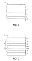
- Illustrated in Figures 1 and 2 are EL devices of the present invention.
- It is the object of the present invention to provide improved EL devices which exhibit high electroluminescence efficiency at relatively low operating voltages of, for example, below 25 volts, such as from 5 to 20 volts, further to provide improved EL devices comprised of an anode, a cathode, and an organic electroluminescent element sandwiched in between the anode and the cathode, and wherein the organic electroluminescent element is comprised of at least one layer containing an indolocarbazole hole transport component, and also to provide EL devices with indolocarbazole compounds which possess excellent hole transporting capability, superior thermal stability, and can be vacuum deposited as thin film EL hole transport components.
- This object is achieved by the EL devices according to
claims 1 and 7. Preferred embodiments are set forth in the subclaims. - In embodiments the present invention provides a layered organic EL devices comprised, for example, of an anode, a cathode, and therebetween the anode and the cathode an organic electroluminescent layer comprising a hole transporting layer containing an indolocarbazole compound, and an electron transporting layer, and which devices possess in embodiments a number of advantages including improved thermal stability, extended service life, high electroluminescence efficiency, superior hole and electron injecting and transporting characteristics, and which devices can be fabricated by vacuum deposition techniques. The EL devices of the present invention provide, for example, improved thermal and operational stability and excellent device durability at temperatures equal to, or above 45°C (degrees Centigrade) such as from 50°C to 95°C.
- In embodiments, the present invention relates to organic EL devices that are comprised in sequence of an anode, a charge, especially hole transporting layer, an electron transporting layer, and a cathode, and wherein the transporting layer contains at least an indolocarbazole compound represented by the following Formulas (I) or (II); or optionally mixtures thereof
 wherein R and R' are independently selected from the group consisting of hydrogen, halogen, alkyl with, for example, from 1 to 25 carbon atoms, alkoxy with, for example, from 1 to 25 carbon atoms, aryl with, for example, from 6 to 30 carbon atoms, and fused aromatic rings such as benzo; m and n are preferably integers, or numbers of 0 to 4; A1 and A2 are arylene with, for example, from 6, preferably 7, to 31 carbon atoms, such as phenylene, tolylene, biphenylene; Ar1, Ar2, Ar3, and Ar4 are aryl, such as those aryl groups with, for example, from 6 to 30 carbon atoms independently selected from the group consisting of, for example, phenyl, tolyl, xylyl, chlorophenyl, alkoxyphenyl, and naphthyl ; R1 and R2 are independently selected from the group consisting of hydrogen, halogen, alkyl with, for example, from 1 to 25 carbon atoms, alkoxyl, or aryl; and p is preferably a number of from 1 to 3.
- The present invention provides also an EL device comprised of a supporting substrate, an anode, a hole transporting layer, an electron transporting layer, and a cathode, wherein said anode is of a thickness ranging from 30 nanometers to 100 nanometers, said hole transport layer contains at least one indolocarbazole compound of the Formulas (I) or (II) with a thickness ranging from 10 nanometers to 100 nanometers, said electron transporting layer is of a thickness ranging from 10 nanometers to 100 nanometers, and said cathode is of a thickness ranging from 10 nanometers to 200 nanometers. Preferably, said anode is indium tin oxide, and said cathode is a magnesium silver alloy. It is also preferred that said electron transporting layer is comprised of a metal chelate compound of 8-hydroxyquinoline.
- Figure 1 illustrates an EL device structure or an organic
light emitting diode 1 comprised of a supportingsubstrate 2 of, for example, glass, ananode 3, an organichole transporting layer 4 comprised of at least one of the indolocarbazoles of the formulas illustrated herein, and preferably indolocarbazoles of Formula (I), an organicelectron transporting layer 5, and in contact therewith a low work function, for example from 2.5 eV to 4.0 eV, metal as acathode 6. In this EL device, a junction is formed between the hole transporting zone and the electron transporting zone. In operation, when the anode is electrically biased to a positive potential with respect to the cathode, holes are injected into the organic hole transporting zone and transported across this zone to said junction. Concurrently, electrons are injected from the cathode into the electron transporting zone and are transported toward the same junction. The recombination of holes and electron occurs near the junction resulting in light emission. - In another embodiment as illustrated in Figure 2, the light emitting diode, or
EL device 1 is comprised of a supportingsubstrate 2 of, for example, glass, ananode 3, an organichole transporting zone 4 comprised oflayers layers 5a and 5b, and in contact therewith a low workfunction metal cathode 6. In this device structure, the transporting zone is comprised of one or more transport layers as compared to the single-layer transporting zone of the device structure of Figure 1. Specifically, thehole transporting zone 4 of Figure 2 is comprised of alayer 4a which facilitates hole injection, and alayer 4b which transports hole carriers. Theelectron transporting zone 5 is comprised of alayer 5a which facilitates electron injection, and a layer 5b which transports electrons. Theselayers - Illustrative examples of the supporting substrate include polymeric components, glass and the like, and more specifically, polyesters like MYLAR®, polycarbonates, polyacrylates, polymethacrylates, polysulfones, and quartz. Other substrates can also be selected providing, for example, material selected can effectively support the other layers, and that it does not interfere with the device functional performance. The thickness of the substrate can be, for example, from 25 to 2,000 microns, and more specifically, from 50 to 1,000 microns, depending, for example, on the structural demands of the device.
- Examples of the anode, which is contiguous to, and in contact with the substrate, include positive charge injecting electrodes, such as indium tin oxide, tin oxide, gold, platinum, or other suitable materials, such electrically conductive carbon, π-conjugated polymers, such as polyaniline, polypyrrole, with a work function equal to, or greater than 4, and more specifically, from 4.0 to 6.5 electron volts. The thickness of the anode can range from, for example, 10 to 5,000Å with the preferred range being dictated by the optical constants of the anode material. One preferred range of thickness is from 20 to 1,000 Angstroms.
- The
hole transporting layer 4 illustrated herein can be of a number of different convenient forms. For example, this layer may be comprised of one layer comprising one or more of hole transport components, at least one of which is an indolocarbazole compound. In another preferred form,layer 4 may be laminately formed from alayer 4a in contact with the anode, and which layer contains a component which facilitates hole injection, and alayer 4b containing the indolocarbazole hole transport component. Any suitable materials which can assist with hole injection from the anode may be employed inlayer 4a, with the preferred materials being the porphyrin derivatives which are disclosed in U.S. Patent 4,720,432. Representative examples of porphyrin derivatives thereof are porphyrin; 1,10,15,20-tetraphenyl-21H,23H-porphyrin copper (II); copper phthalocyanine, copper tetramethyl phthalocyanine; zinc phthalocyanine; titanium oxide phthalocyanine; magnesium phthalocyanine. - In embodiments, the
hole transporting layer 4 contains at least one indolocarbazole compound as represented by Formula (I) or (II). The indolocarbazole compounds of the present invention generally contain a structurally rigid indolocarbazole nucleus, and offer a number of advantages as illustrated herein as they possess, for example, a high glass transition temperature, and are capable of forming thermally and morphologically stable thin films by vacuum evaporation techniques. - Specific examples of arylene groups, A1 and A2 in Formula (I) or (II) include those illustrated by Formulas A-1 through A-8, and their substituted derivatives with substituents being selected from, for example, the group consisting of alkyl with 1 to 5 carbon atoms, phenyl, and aryl with a substituent of halogen atom, alkyl or alkoxy with 1 to 5 carbons,


- Illustrative examples of indolocarbazole compounds (I) and (II) which can be selected for use in the EL devices of the present invention are as follows, with 1, 2, 3, 4, 5, 6, 12, 13 and 17 being preferred in embodiments: 5,11-bis[4'-(3-methyldiphenylamino)-1,1'-biphenyl-4-yl]-5,11-dihydroindolo[3,2-b]carbazole; 5,11-bis[4'-(4-methyldiphenylamino)-1,1'-biphenyl-4-yl]-5,11-dihydroindolo[3,2-b]carbazole; 5,11-bis[4'-(diphenylamino)-1,1'-biphenyl-4-yl]-5,11-dihydroindolo[3,2-b]carbazole; 5,11-bis[4'-(di-p-tolylamino)-1,1'-biphenyl-4-yl]-5,11-dihydroindolo[3,2-b] carbazole; 5,11-bis[4'-(3,4-dimethyldiphenylamino)-1,1'-biphenyl-4-yl]-5,11-dihydroindolo[3,2-b]carbazole; 5,11-bis[4'-(3-methoxydiphenylamino)-1,1'-biphenyl-4-yl]-5,11-dihydroindolo[3,2-b]carbazole; 5,11-bis[4'-(3-chlorodiphenylamino)-1,1'-biphenyl-4-yl]-5,11-dihydroindolo[3,2-b]carbazole; 5,11-bis[4'-(4-chlorodiphenylamino)-1,1'-biphenyl-4-yl]-5,11-dihydroindolo [3,2-b]carbazole; 5,11-bis[4'-(diphenylamino)-1,1'-biphenyl-yl]-2,8-dimethyl-5,11-dihydroindolo[3,2-b]carbazole; 5,11-bis[4'-(4-methyldiphenyl amino)-1,1 '-biphenyl-4-yl]-2,8-dimethyl-5,11-dihydroindolo[3,2-b]carbazole; 5,11-bis[4-(diphenylamino)phenyl]-5,11-dihydroindolo[3,2-b]carbazole; 5,11-bis[4-(3-methyldiphenylamino)phenyl]-5,11-dihydroindolo[3,2-b]carbazole; 5,11-bis[4-(4-methyldiphenylamino)phenyl]-5,11-dihydroindolo[3,2-b]carbazole; 5,11-bis[4-(diphenylamino)phenyl]-2,8-dimethyl-5,11-dihydroindolo[3,2-b]carbazole; 5,11-bis[4-(4-methyldiphenylamino)phenyl]-2,8-dimethyl-5,11-dihydroindolo[3,2-b]carbazole; 5,11-bis[4-1-naphthyl phenylamino)phenyl]-5,11-dihydroindolo[3,2-b]carbazole.
- Those described by Formula (II) include 5,7-bis[4'-(3-methyldiphenylamino)-1,1'-biphenyl-4-yl]-5,7-dihydroindolo[2,3-b]carbazole; 5,7-bis[4'-(diphenylamino)-1,1'-biphenyl-4-yl]-5,7-dihydroindolo[2,3-b] carbazole; 5,7-bis[4'-(di-p-tolylamino)-1,1'-biphenyl-4-yl]-5,7-dihydroindolo [2,3-b]carbazole; 5,7-bis[4'-(3,4-dimethyldiphenylamino)-1,1'-biphenyl-4-yl]-5,7-dihydroindolo[2,3-b]carbazole; 5,7-bis[4'-(diphenylamino)-1,1'-biphenyl-4-yl]-2,10-dimethyl-5,7-dihydroindolo[2,3-b]carbazole; 5,7-bis[4-(diphenylamino)phenyl]-5,7-dihydroindolo[2,3-b]carbazole; 5,7-bis[4-(3-methyldiphenylamino)phenyl]-5,7-dihydroindolo[2,3-b]carbazole; 5,7-bis[4-(diphenylamino)phenyl]-2,10-dimethyl-5,7-dihydroindolo[2,3-b]carbazole.


- Similarly, the electron transporting layer or
zone 5 may be of a number of different suitable, or convenient forms of, for example, a single layer or a dual-layer structure. Any suitable electron transport compounds may be utilized in this zone. Examples of useful electron transport compounds include fused ring luminescent materials, such as anthracene, phenanthracene, pyrene, perylene, as illustrated in U.S. Patent 3,172,862; butadienes such as 1,4-diphenylbutadiene and tetraphenylbutadiene, and stilbenes, as illustrated in U.S. Patent 4,356,429 and 5,516,577; optical brightness such as those disclosed by U.S. Patent 4,539,507. - Preferred electron transport materials are metal chelates of 8-hydroxyquinoline as disclosed in U.S. Patents 4,539,507; 5,151,629, and 5,150,006. Illustrative examples of the metal chelates include tris(8-hydroxyquinolinate)aluminum (AlQ3), tris(8-hydroxyquinolinate)gallium, bis(8-hydroxyquinolinate)magnesium, bis(8-hydroxyquinolinate)zinc, tris(5-methyl-8-hydroxyquinolinate)aluminum, tris(7-propyl-8-quinolinolato) aluminum, bis[benzo{f}-8-quinolinate]zinc, bis(10-hydroxybenzo[h] quinolinate)beryllium, bis(2-methylquinolinolato)aluminum-µ-oxo-bis(2-methyl-8-quinolinolato)aluminum, bis(2-methyl-8-quinolinolato)(phenolato) aluminum, bis(2-methyl-8-quinolinolato)(para-phenylphenolato)aluminum, bis(2-methyl-8-quinolinolato)(2-naphthalolato)aluminum.
- Another class of preferred electron transport materials are the metal chelates disclosed in copending application U.S. Serial No. 829,398, represented by the following formulawherein Ar is an aryl group containing, for example, 6 to 30 carbon atoms or an aromatic heterocyclic group such as, for example, pyridyl, quinolyl, thienyl ; X is selected from the group consisting of oxygen, sulfur, and selenium; N is nitrogen, O is oxygen, and Z is an aromatic component, such as for example 1,2-phenylene, 1,2-naphthylene, 2,3-naphthylene, 3,4-pyridinediyl, 3,4-quinolinediyl, the substituted analogs thereof with the substituents being preferably alkyl containing 1 to 5 carbon atoms, phenyl or aryl with a substituent of halogen, alkyl or alkoxy groups containing 1 to 5 carbons, halogen, alkoxy groups containing 1 to 3 carbon atoms, a carboxy group, or a cyano group.

- The metal ion of Formula (III) may be monovalent, divalent, or trivalent. Illustrative examples of metal ions include those which are, for example, capable of forming a stable chelate compound with the ligand, such as, for example, lithium, sodium, beryllium, magnesium, zinc, and the like, with the preferred metal ions being beryllium and zinc. Illustrative examples of metal chelate compounds (III) include bis[2-(2-hydroxyphenyl)-5-phenyl-1,3,4-oxadiazolato]zinc; bis[2-(2-hydroxyphenyl)-5-phenyl-1,3,4-oxadiazolato]beryllium; bis[2-(2-hydroxyphenyl)-5-(1-naphthyl)-1,3,4-oxadiazolato]zinc; bis[2-(2-hydroxyphenyl)-5-(1-naphthyl)-1,3,4-oxadiazolato]beryllium; bis[5-biphenyl-2-(2-hydroxyphenyl)-1,3,4-oxadiazolato]zinc; bis[5-biphenyl-2-(2-hydroxyphenyl)-1,3,4-oxadiazolato] beryllium; bis(2-hydroxyphenyl)-5-phenyl-1,3,4-oxadiazolato] lithium; bis[2-(2-hydroxyphenyl)-5-p-tolyl-1,3,4-oxadiazolato]zinc; bis[2-(2-hydroxyphenyl)-5-p-tolyl-1,3,4-oxadiazolato]beryllium.
- In embodiments of the present invention, the total thickness of the luminescent medium, which includes the
hole transporting zone 4 and theelectron transporting zone 5, is preferably less than 1 micron, and more specifically, from 0.05 to 1 micron, primarily to maintain a current density conducive to efficient light emission under a relatively low applied voltage across the electrodes. For instance, in the device of Figure 1, suitable thicknesses of the hole transporting layer, or zone can range from 40 to 2,000 Å, with the preferred thickness being from 100 to 800 Å, while the thickness of the electron transporting layer, or zone can range from 50 to 2,000 Å, with the preferred thickness being from 100 to 800 Å. In the device of Figure 2, the thickness of the hole injecting layer can range from 25 to 1,000 Å, with the preferred thickness being from 50 to 800 Å, and the hole transporting layer thickness can range from 25 to 1,000 Å, with the preferred thickness being from 50 to 800 Å. Similarly, the electron transporting layer can range in thickness of from 25 to 1,000 Å, with the preferred thickness being from 50 to 800 Å, and the electron injecting layer thickness can range from 25 to 1000 Å, with the preferred thickness being from 50 to 800 Å. - The
cathode 6 can be comprised of any metal, including high or low work function metals. The cathode can be derived from a combination of a low work function metal, for example less than 4 eV, such as from 2 to 4 eV and at least one other metal. Effective proportions of the low work function metal to the second metal are from less than 0.1 percent to 99.9 percent by weight. Illustrative examples of low work function metals include alkaline metals, such as lithium or sodium, Group 2A or alkaline earth metals, such as beryllium, magnesium, calcium, or barium, and Group III metals including rare earth metals and the actinide group metals, such as scandium, yettrium, lanthanium, cerium, europium, terbium, or actinium. Lithium, magnesium and calcium are the preferred low work function metals. - The thickness of
cathode 6 ranges from, for example, 10 to 5,000 Å. The Mg:Ag cathodes, reference U.S. Patent 4,885,211, constitute one preferred cathode construction. In embodiments, preferred cathode examples are as illustrated in U.S. Patent 5,429,884, wherein the cathodes are formed from lithium alloys with other high work function metals such as aluminum and indium. - Both
anode 3 andcathode 6 of the EL devices of the present invention can be of any convenient forms. A thin conductive layer can be coated onto a light transmissive substrate, for example a transparent or substantially transparent glass plate or plastic film. The EL device can include alight transmissive anode 3 formed from tin oxide or indium tin oxide coated on a glass plate. Also, very thin, for example less than 200 Å, light-transparent metallic anodes can be used, such as gold, palladium, and the like. In addition, a transparent or semitransparent thin layer of conductive carbon or conjugated polymers such as polyaniline, polypyrrole, can be used as anodes. Additional suitable forms of theanode 3 andcathode 6 are illustrated in U.S. Patent 4,720,432. - The indolocarbazole hole transport compounds can be prepared by Ullmann condensation of the corresponding dihydroindolocarbazole precursors selected from those represented by formulas (IBC) through (VIb) with aryl halide and a suitable known arylamine, such as a halo, like iodo alkylarylamino biphenyl in the presence of a copper catalyst, especially a ligand copper catalyst as illustrated in U.S. Patents 5,538,829; 5,648,542; 5,654,482 and 5,648,539. Specific examples of dihydroindolocarbazoles, which can be readily obtained by known literature processes, are 5,11-dihydroindolo [3,2-b]carbazole, 5,7-dihydroindolo[2,3-b]carbazole, 5,12-dihydroindolo [3,2-c]carbazole, 5,10-dihydroindolo[3,2-a]carbazole, 11,12-dihydroindolo [2,3-a]carbazole.
- Illustrative examples of aryl halides that can be utilized for the Ullmann condensation are iodobenzene, 3-iodotoluene, 4-iodotoluene, 4-iodo-1,2-xylene, 1-iodonaphthalene, 2-iodonaphthalene, 4-iodobiphenyl, 4-iodo-4'-(3-methyldiphenylamino)-1,1'-biphenyl, 4-iodo-4'-(diphenylamino)-1,1'-biphenyl, N, N-Biphenyl-4-iodoaniline, and N-phenyl-N-3-tolyl-4-iodoaniline. The Ullmann condensation is generally accomplished in an inert solvent, such as dodecane, tridecance, xylene, sulfolane, high boiling petroleum ethers with boiling point of, for example, over 150°C, at a reaction temperature ranging from 90°C to 300°C, and preferably from 150°C to 250°C. Any copper catalysts suitable for the Ullmann condensation, including copper powder, copper (I) oxide, copper (I) chloride, copper (II) sulfate, copper (II) acetate, may be employed for the process of the present invention, inclusive of the ligand copper catalysts as illustrated in the copending applications recited herein being preferred. An effective molar ratio of the copper catalyst to the dihydroindolocarbazole compound ranges, for example, from 0.01 to 0.5. The condensation reaction can be greatly accelerated with a base, such as for example an alkaline metal hydroxide or carbonate, including potassium hydroxide, potassium carbonate and sodium hydroxide. After the condensation, the reaction mixture is cooled down to room temperature, and the product is isolated by known separation techniques such as, for example, by filtration and chromatography. The product is generally characterized by known analytical techniques such as IR and NMR.
- The substituents, such as for example R and R', can be positioned at various different appropriate locations on the aromatic components, like the benzene ring.
- A 100 milliliter 3-necked round bottom flask equipped with a mechanical stirrer, reflux condenser, and argon inlet was purged with argon and then charged with 5,11-dihydroindolo[3,2-b]carbazole (1.65 grams, 6.45 mmol), 4-iodo-4'-(3-methyldiphenylamino)-1,1'-biphenyl (7.1 grams, 15.5 mmol), copper sulfate pentahydrate (0.12 gram, 0.5 mmol), potassium carbonate (2.1 grams, 15.2 mmol), and n-tridecane (5.0 milliliters). Under an argon atmosphere, the reaction mixture was then heated to about 250°C with a heating mantle and allowed to proceed at that temperature until chromatographic analysis indicated that the reaction was complete after approximately 6 hours. The heating mantle was removed and the resulting mixture was cooled to 25°C. The solids were separated and washed with water, and collected by filtration. The crude product was chromatographed on alumina using hot toluene as an eluant to provide in a pure form, 99.7 percent pure, the titled product. Yield: 3.45 grams. The glass transition temperature of this compound was 160°C. IR (Kbr): 1,598, 1,495, 1,450, 1,320, 1,291, 1,277, 1,232, 742, 695 cm-1. 1H-NMR (DMSO-d6-CDCl3): δ 2.30 (s), 6.88∼7.51 (m), 7.66 (d, J=8.6 Hz), 7.76 (d, J=8.6 Hz), 7.93 (d, J=8.6 Hz), 7.99 (s), 8.17 (s), 8.19 (d, J=8.6 Hz).
- A 100 milliliter 3-necked round bottom flask equipped with a mechanical stirrer, reflux condenser, and argon inlet was purged with argon and then charged with 5,11-dihydroindolo[3,2-b]carbazole (5.0 grams, 19.5 mmol), 4-(3-methyldiphenylamino)iodobenzene (15.5 grams, 40.54 mmol), copper sulfate pentahydrate (0.24 gram, 0.96 mmol), potassium carbonate (5.59 grams, 40.5 mmol), and n-tridecane (10.0 milliliters). Under an argon atmosphere, the reaction mixture was heated to about 250°C with a heating mantle and allowed to proceed at that temperature until chromatographic analysis indicated that the reaction was complete after approximately 6 hours. The heating mantle was removed and the resulting mixture was cooled to 25°C. The solids were washed with water, and collected by filtration. The crude product was chromatographed on alumina using hot toluene as an eluant to provide in a pure form, 99.7 percent pure, the titled product. Yield: 7.50 grams. The glass transition temperature of this compound was 125°C. IR (Kbr): 1,584, 1,510, 1,451, 1,311, 1,274, 1,230, 843, 759, 742, 692 cm-1. 1H-NMR (DMSO-d6-CDCl3): δ 2.34 (s), 6.93 (d, J=8.7 Hz), 7.02∼7.52 (m), 7.82 (s), 8.09 (s), 8.17 (d, J=8.6 Hz).
- An organic EL was prepared as follows:
- 1. An indium tin oxide (ITO, 50 nanometers thickness) coated glass (1.0 millimeter thickness) was cleaned with a commercial detergent, rinsed with deionized water and dried in a vacuum over at 60°C for 1 hour. Immediately before use, the glass was treated with UV ozone for 0.5 hour.
- 2. The ITO substrate was placed in a vacuum deposition
chamber. The deposition rate and layer thickness were controlled by an
Inficon Model IC/5 controller. Under a pressure of about 5x10⁻⁶ torr the
indolocarbazole compound 5,11-bis[4'-(3-methyldiphenylamino)-1,1'-biphenyl-4-yl]-5,11-dihydroindolo[3,2-b]carbazole obtained from Example I was evaporated from an electrically heated tantalum boat to deposit a 80 nanometer hole transporting layer on the ITO. The deposition rate of the indocarbazole compound was controlled at 0.6 nanometer/second. - 3. Onto the indolocarbazole layer was deposited tris(8-hydroxyquinolinate)aluminum at an evaporation rate of 0.6 nanometer/second to form an 80 nanometer electron transporting layer which also acts as luminescent layer.
- 4. A 100 nanometer magnesium silver cathode alloy was deposited at a total deposition rate of 0.5 nanometer/second onto the electron injecting and transporting layer by simultaneous evaporation from two independently controlled tantalum boats containing Mg and Ag, respectively. The typical composition was 9:1 in atomic ratio of Mg to Ag. Finally, a 200 nanometer silver layer was overcoated on the Mg:Ag cathode for the purpose of protecting the reactive Mg from ambient moisture.
-
- The device as prepared above was retained in a dry box which was continuously purged with nitrogen gas. Its performance was assessed by measuring its current-voltage characteristics and light output under a direct current measurement. The current-voltage characteristics were determined with a Keithley Model 238 High Current Source Measure Unit. The ITO electrode was always connected to the positive terminal of the current source. At the same time, the light output from the device was monitored by a silicon photodiode.
- The performance characteristics of the above EL device were evaluated under a constant current density of 25 mA/cm2. The EL device provided an initial light intensity of 590 cd/m2 at 9.2 volts, a level which was well in excess of that required for display applications. The light intensity degraded slowly, with a 50 percent reduction after 350 hours of continuous operation. Furthermore, this device displayed no change in its current-light intensity characteristics even after it was subjected to a temperature of 60°C for 72 hours.
- A comparative EL device was prepared in accordance with the procedure of Example III except that N,N'-bis(3-methylphenyl)-N,N'-diphenyl-4,4'-diaminobiphenyl, a triphenylamine-based hole transport molecule commonly selected for a number of prior art EL devices, was utilized in place of the 5,11-bis[4'-(3-methyldiphenylamino)-1,1'-biphenyl-4-yl]-5,11-dihydroindolo[3,2-b]carbazole. The performance characteristics of this device were evaluated in a similar manner. The device provided an initial light intensity of 570 cd/m2 at an operating voltage of 9.5 volts as measured under a constant current density of 25 mA/cm2. The light intensity degraded rapidly, and registered a 50 percent reduction after 90 hours of continuous operation. Furthermore, this device displayed substantial change in its current-light intensity characteristics after it was subjected to a temperature of 60°C for 72 hours.
- Another comparative EL device was prepared in accordance with the procedure of Example III except that 1,1-bis(4-ditolylaminophenyl)cyclohexane was utilized in place of the 5,11-bis[4'-(3-methyldiphenylamino)-1,1'-biphenyl-4-yl]-5,11-dihydroindolo[3,2-b] carbazole. The performance characteristics of the device were evaluated in a similar manner. This device provided an initial light intensity of 450 cd/m2 at an operating voltage of 11.5 volts. The light intensity degraded rapidly, and registered a 50 percent reduction after 60 hours of continuous operation.
- An organic EL device was prepared in accordance with Example III except that an additional layer of copper phthalocyanine (15 nanometers) was first deposited on the ITO, and thereover was deposited the indolocarbazole layer to form a hole transporting zone. The device preparation was completed as described in Example III.
- The EL performance characteristics were evaluated under a constant current density of 25 mA/cm2. The device provided an initial light intensity of 520 cd/m2 at 11.5 volts, a level which was well in excess of that required for display applications. The light intensity degraded slowly, with a 50 percent reduction after 450 hours of continuous operation.
- An organic EL device was fabricated in a similar manner as described in Example III. In place of the tris(8-hydroxyquinolinate)aluminum layer, and onto the indolocarbazole hole transporting layer was deposited an 80 nanometer electron transporting layer, also acting as a luminescent zone, through simultaneous evaporation of tris(8-hydroxyquinolinate)aluminum and a fluorescent material of N,N'-dimethyl-2,9-dimethylquinacridone from two independently controlled tantalum boats. The evaporation rates were controlled at 0.6 nanometer/second and 0.006 nanometer/second, respectively. The device preparation was completed by deposition of a Mg:Ag alloy as the cathode as described in Example III.
- The EL performance characteristics were evaluated under a constant current density of 25 mA/cm2. The device emitted a greenish yellow light with an initial light intensity of 950 cd/m2 at 9.3 volts, a level which was well in excess of that required for display applications. The light intensity degraded slowly, with a 50 percent reduction after 530 hours of continuous operation.
- An organic EL device was prepared in accordance with Example III except that 5,11-bis[4-(3-methyldiphenylamino)phenyl]-5,11-dihydroindolo[3,2-b]carbazole obtained from Example II was used as the hole transport component in place of 5,11-bis[4'-(3-methyldiphenylamino)-1,1'-biphenyl-4-yl]-5,11-dihydroindolo[3,2-b]carbazole. The device preparation was completed as described in Example III.
- The EL performance characteristics of the above EL device were evaluated under a constant current density of 25 mA/cm2. The device provided an initial light intensity of 560 cd/m2 at 9.3 volts, a level which was well in excess of that required for display applications. The light intensity degraded slowly, with a 50 percent reduction after 420 hours of continuous operation.
Claims (10)
- An organic electroluminescent (EL) device comprised of a charge transport component of an indolocarbazole compound represented by Formulas (I) or (II)
 wherein R and R' are independently selected from the group consisting of hydrogen, alkyl, alkoxyl, aryl, and halogen; m and n are numbers from 0 to 4; A1 and A2 are arylene; Ar1, Ar2, Ar3, and Ar4 are aryl; R1 and R2 are independently selected from the group consisting of hydrogen, alkyl, alkoxyl, aryl, and halogen; and p is a number from 1 to 3.
- The EL device in accordance with claim 1 wherein R and R' are fused aromatic rings.
- The EL device in accordance with claim 1 or 2 wherein Ar1, Ar2, Ar3, and Ar4 are aryl groups independently selected from the group . consisting of phenyl, tolyl, xylyl, halophenyl, alkoxyphenyl, and naphthyl.
- The EL device in accordance with any of claims 1 to 3 further including an anode and a cathode, and an organic electroluminescent element situated between the anode and cathode, and wherein said organic electroluminescent element comprises said indolocarbazole of Formulas (I) or (II).
- The EL device in accordance with any of claims 3 or 4 wherein R and R' are hydrogen or methyl; A1 and A2 are a phenylene, or a biphenylene; Ar1, Ar2, Ar3, and Ar4 are independently selected from the group consisting of phenyl, tolyl, and xylyl; R1 and R2 are hydrogen; m and n are zero to 4, and p is 1.
- The EL device in accordance with any of claims 1 to 5 wherein said indolocarbazole is selected from the group consisting of 5,11-bis[4'-(3-methyldiphenylamino)-1,1'-biphenyl-4-yl]-5,11-dihydroindolo[3,2-b] carbazole, 5,11-bis[4'-(4-methyldiphenylamino)-1,1'-biphenyl-yl]-5,11-dihydroindolo[3,2-b]carbazole, 5,11-bis[4'-(diphenylamino)-1,1'-biphenyl-4-yl]-5,11-dihydroindolo[3,2-b]carbazole, 5,11-bis[4'-(3-methoxydiphenyl amino)-1,1'-biphenyl4-yl]-5,11-dihydroindolo[3,2-b]carbazole, 5,11-bis[4'-(diphenylamino)-1,1'-biphenyl-4-yl]-2,8-dimethyl-5,11-dihydroindolo[3,2-b] carbazole, 5,11-bis[4-(diphenylamino)phenyl]-5,11-dihydroindolo[3,2-b] carbazole, 5,11-bis[4-(3-methyldiphenylamino)phenyl]-5,11-dihydroindolo [3,2-b]carbazole, and 5,11-bis[4-(4-methyldiphenylamino)phenyl]-5,11-dihydroindolo[3,2-b]carbazole.
- An EL device comprised of a supporting substrate, an anode, a hole transporting layer, an electron transporting layer, and a cathode, wherein said anode is of a thickness ranging from 30 nanometers to 100 nanometers, said hole transport layer contains at least one indolocarbazole compound of the Formulas (I) or (II) with a thickness ranging from 10 nanometers to 100 nanometers, said electron transporting layer is of a thickness ranging from 10 nanometers to 100 nanometers, and said cathode is of a thickness ranging from 10 nanometers to 200 nanometers.
- The EL device in accordance with claim 7 wherein said anode is indium tin oxide, and said cathode is a magnesium silver alloy or a lithium aluminum alloy.
- An EL device in accordance with claim 7 or 8 wherein said electron transporting layer is comprised of a metal chelate compound of 8-hydroxyquinoline.
- The EL device in accordance with any of claims 7 to 9 wherein said indolocarbazole is 5,11-bis[4'-(3-methyldiphenylamino)-1,1'-biphenyl-4-yl]-5,11-dihydroindolo[3,2-b]carbazole, 5,11-bis[4'-(4-methyldiphenylamino)-1,1'-biphenyl-4-yl]-5,11-dihydroindolo[3,2-b]carbazole, 5,11-bis[4'-(3-methoxydiphenylamino)-1,1'-biphenyl-4-yl]-5,11-dihydroindolo[3,2-b] carbazole, 5,11-bis[4-(diphenylamino)phenyl]-5,11-dihydroindolo[3,2-b] carbazole, or 5,11-bis[4-(3-methyldiphenylamino)phenyl]-5,11-dihydroindolo[3,2-b]carbazole.
Applications Claiming Priority (2)
| Application Number | Priority Date | Filing Date | Title |
|---|---|---|---|
| US942882 | 1992-09-11 | ||
| US08/942,882 US5952115A (en) | 1997-10-02 | 1997-10-02 | Electroluminescent devices |
Publications (2)
| Publication Number | Publication Date |
|---|---|
| EP0906948A1 EP0906948A1 (en) | 1999-04-07 |
| EP0906948B1 true EP0906948B1 (en) | 2003-02-12 |
Family
ID=25478759
Family Applications (1)
| Application Number | Title | Priority Date | Filing Date |
|---|---|---|---|
| EP98117913A Expired - Lifetime EP0906948B1 (en) | 1997-10-02 | 1998-09-22 | Electroluminescent devices |
Country Status (4)
| Country | Link |
|---|---|
| US (1) | US5952115A (en) |
| EP (1) | EP0906948B1 (en) |
| JP (1) | JP4243876B2 (en) |
| DE (1) | DE69811303T2 (en) |
Cited By (14)
| Publication number | Priority date | Publication date | Assignee | Title |
|---|---|---|---|---|
| WO2011076326A1 (en) | 2009-12-22 | 2011-06-30 | Merck Patent Gmbh | Electroluminescent functional surfactants |
| WO2011076323A1 (en) | 2009-12-22 | 2011-06-30 | Merck Patent Gmbh | Formulations comprising phase-separated functional materials |
| WO2011076314A1 (en) | 2009-12-22 | 2011-06-30 | Merck Patent Gmbh | Electroluminescent formulations |
| WO2011110275A2 (en) | 2010-03-11 | 2011-09-15 | Merck Patent Gmbh | Radiative fibers |
| WO2011147522A1 (en) | 2010-05-27 | 2011-12-01 | Merck Patent Gmbh | Compositions comprising quantum dots |
| WO2012013270A1 (en) | 2010-07-26 | 2012-02-02 | Merck Patent Gmbh | Nanocrystals in devices |
| WO2012013272A1 (en) | 2010-07-26 | 2012-02-02 | Merck Patent Gmbh | Quantum dots and hosts |
| WO2012110178A1 (en) | 2011-02-14 | 2012-08-23 | Merck Patent Gmbh | Device and method for treatment of cells and cell tissue |
| WO2012126566A1 (en) | 2011-03-24 | 2012-09-27 | Merck Patent Gmbh | Organic ionic functional materials |
| WO2012149992A1 (en) | 2011-05-04 | 2012-11-08 | Merck Patent Gmbh | Device for preserving fresh goods |
| WO2012152366A1 (en) | 2011-05-12 | 2012-11-15 | Merck Patent Gmbh | Organic ionic compounds, compositions and electronic devices |
| WO2021213917A1 (en) | 2020-04-21 | 2021-10-28 | Merck Patent Gmbh | Emulsions comprising organic functional materials |
| WO2023012084A1 (en) | 2021-08-02 | 2023-02-09 | Merck Patent Gmbh | A printing method by combining inks |
| WO2023237458A1 (en) | 2022-06-07 | 2023-12-14 | Merck Patent Gmbh | Method of printing a functional layer of an electronic device by combining inks |
Families Citing this family (103)
| Publication number | Priority date | Publication date | Assignee | Title |
|---|---|---|---|---|
| US6229012B1 (en) | 1998-10-01 | 2001-05-08 | Xerox Corporation | Triazine compositions |
| US6821643B1 (en) | 2000-01-21 | 2004-11-23 | Xerox Corporation | Electroluminescent (EL) devices |
| US6225467B1 (en) | 2000-01-21 | 2001-05-01 | Xerox Corporation | Electroluminescent (EL) devices |
| US6734623B1 (en) | 2000-07-31 | 2004-05-11 | Xerox Corporation | Annealed organic light emitting devices and method of annealing organic light emitting devices |
| US6765348B2 (en) | 2001-01-26 | 2004-07-20 | Xerox Corporation | Electroluminescent devices containing thermal protective layers |
| US6479172B2 (en) | 2001-01-26 | 2002-11-12 | Xerox Corporation | Electroluminescent (EL) devices |
| US7288887B2 (en) * | 2001-03-08 | 2007-10-30 | Lg.Philips Lcd Co. Ltd. | Devices with multiple organic-metal mixed layers |
| US6841932B2 (en) | 2001-03-08 | 2005-01-11 | Xerox Corporation | Display devices with organic-metal mixed layer |
| US6753098B2 (en) | 2001-11-08 | 2004-06-22 | Xerox Corporation | Organic light emitting devices |
| US6759146B2 (en) | 2001-11-08 | 2004-07-06 | Xerox Corporation | Organic devices |
| US6740429B2 (en) | 2001-11-08 | 2004-05-25 | Xerox Corporation | Organic light emitting devices |
| US6737177B2 (en) | 2001-11-08 | 2004-05-18 | Xerox Corporation | Red organic light emitting devices |
| US6773830B2 (en) | 2001-11-08 | 2004-08-10 | Xerox Corporation | Green organic light emitting devices |
| US7179147B2 (en) * | 2003-04-24 | 2007-02-20 | Semiconductor Energy Laboratory Co., Ltd. | Manufacturing method of electroluminescent device |
| US20040247933A1 (en) * | 2003-06-03 | 2004-12-09 | Canon Kabushiki Kaisha | Bipolar asymmetric carbazole-based host materials for electrophosphorescent guest-host OLED systems |
| US9085729B2 (en) * | 2004-02-09 | 2015-07-21 | Lg Display Co., Ltd. | Blue emitters for use in organic electroluminescence devices |
| US7629695B2 (en) * | 2004-05-20 | 2009-12-08 | Kabushiki Kaisha Toshiba | Stacked electronic component and manufacturing method thereof |
| US7456424B2 (en) * | 2004-12-14 | 2008-11-25 | Xerox Corporation | Thin film transistors including indolocarbozoles |
| US7396852B2 (en) | 2005-11-16 | 2008-07-08 | Xerox Corporation | Compound having indolocarbazole moiety and divalent linkage |
| US7829727B2 (en) * | 2005-11-16 | 2010-11-09 | Xerox Corporation | Device containing compound having indolocarbazole moiety and divalent linkage |
| US7402681B2 (en) | 2004-12-14 | 2008-07-22 | Xerox Corporation | Compound with indolocarbazole moieties and devices containing such compound |
| US7449831B2 (en) | 2004-08-02 | 2008-11-11 | Lg Display Co., Ltd. | OLEDs having inorganic material containing anode capping layer |
| KR101030010B1 (en) | 2004-09-18 | 2011-04-20 | 삼성모바일디스플레이주식회사 | Blue electroluminescent polymer and organoelectroluminescent device employing the same |
| GB0424294D0 (en) * | 2004-11-03 | 2004-12-01 | Elam T Ltd | Buffer layer |
| US7402346B2 (en) * | 2004-12-07 | 2008-07-22 | Lg. Philips Lcd Co., Ltd. | Organic electroluminescent devices |
| US20060124921A1 (en) * | 2004-12-14 | 2006-06-15 | Xerox Corporation | Compound with indolocarbazole moieties and devices containing such compound |
| US20060125009A1 (en) | 2004-12-14 | 2006-06-15 | Xerox Corporation | Thin film transistors including indolocarbazoles |
| US7173140B2 (en) | 2004-12-14 | 2007-02-06 | Xerox Corporation | Process to form compound with indolocarbazole moieties |
| US8217181B2 (en) | 2004-12-30 | 2012-07-10 | E. I. Du Pont De Nemours And Company | Dihalogen indolocarbazole monomers and poly (indolocarbazoles) |
| WO2006100896A1 (en) | 2005-03-18 | 2006-09-28 | Idemitsu Kosan Co., Ltd. | Aromatic amine derivative and organic electroluminescence device utilizing the same |
| US8487527B2 (en) * | 2005-05-04 | 2013-07-16 | Lg Display Co., Ltd. | Organic light emitting devices |
| US7777407B2 (en) * | 2005-05-04 | 2010-08-17 | Lg Display Co., Ltd. | Organic light emitting devices comprising a doped triazine electron transport layer |
| US7728517B2 (en) * | 2005-05-20 | 2010-06-01 | Lg Display Co., Ltd. | Intermediate electrodes for stacked OLEDs |
| US7943244B2 (en) * | 2005-05-20 | 2011-05-17 | Lg Display Co., Ltd. | Display device with metal-organic mixed layer anodes |
| US7811679B2 (en) * | 2005-05-20 | 2010-10-12 | Lg Display Co., Ltd. | Display devices with light absorbing metal nanoparticle layers |
| US7750561B2 (en) * | 2005-05-20 | 2010-07-06 | Lg Display Co., Ltd. | Stacked OLED structure |
| US7795806B2 (en) * | 2005-05-20 | 2010-09-14 | Lg Display Co., Ltd. | Reduced reflectance display devices containing a thin-layer metal-organic mixed layer (MOML) |
| US20070111027A1 (en) * | 2005-07-29 | 2007-05-17 | Chen Shaw H | Light-emitting organic materials |
| WO2007063754A1 (en) * | 2005-12-01 | 2007-06-07 | Nippon Steel Chemical Co., Ltd. | Compound for organic electroluminescent element and organic electroluminescent element |
| US7352125B2 (en) * | 2005-12-21 | 2008-04-01 | Lg.Philips Lcd Co., Ltd. | Organic light emitting devices with hole impeding materials |
| US7977862B2 (en) * | 2005-12-21 | 2011-07-12 | Lg Display Co., Ltd. | Organic light emitting devices |
| US7645525B2 (en) * | 2005-12-27 | 2010-01-12 | Lg Display Co., Ltd. | Organic light emitting devices |
| KR100955993B1 (en) | 2006-11-09 | 2010-05-04 | 신닛테츠가가쿠 가부시키가이샤 | Compound for organic electroluminescent device and organic electroluminescent device |
| JP4886483B2 (en) * | 2006-11-22 | 2012-02-29 | 株式会社リコー | Electrostatic latent image carrier, process cartridge, image forming apparatus, and image forming method |
| TWI468489B (en) | 2007-05-29 | 2015-01-11 | Nippon Steel & Sumikin Chem Co | Organic electroluminescent element compounds and organic electroluminescent elements |
| CN101679852B (en) * | 2007-05-30 | 2012-12-05 | 新日铁化学株式会社 | Compound for organic electroluminescent device and organic electroluminescent device |
| TWI472074B (en) * | 2008-03-17 | 2015-02-01 | Nippon Steel & Sumikin Chem Co | Organic electroluminescent elements |
| KR101571114B1 (en) * | 2008-05-08 | 2015-11-23 | 신닛테츠 수미킨 가가쿠 가부시키가이샤 | Compound for organic electroluminescent elements and organic electroluminescent element |
| CN102017220B (en) | 2008-05-08 | 2012-11-07 | 新日铁化学株式会社 | Compound for organic electric field light-emitting element and organic electric field light-emitting element |
| WO2009148015A1 (en) * | 2008-06-05 | 2009-12-10 | 出光興産株式会社 | Halogen compound, polycyclic compound, and organic electroluminescence element comprising the polycyclic compound |
| US8049411B2 (en) | 2008-06-05 | 2011-11-01 | Idemitsu Kosan Co., Ltd. | Material for organic electroluminescence device and organic electroluminescence device using the same |
| TWI471405B (en) | 2009-03-31 | 2015-02-01 | Nippon Steel & Sumikin Chem Co | A phosphorescent element material, and an organic electroluminescent device using the same |
| JP5723764B2 (en) * | 2009-03-31 | 2015-05-27 | 新日鉄住金化学株式会社 | Organic electroluminescence device |
| JP4870245B2 (en) | 2009-03-31 | 2012-02-08 | 新日鐵化学株式会社 | Phosphorescent light emitting device material and organic electroluminescent device using the same |
| KR101174088B1 (en) * | 2009-06-25 | 2012-08-14 | 제일모직주식회사 | Compounds?for organic photoelectric?device and organic photoelectric?device containing the same |
| KR101333694B1 (en) * | 2009-06-25 | 2013-11-27 | 제일모직주식회사 | Compounds for organic photoelectric device and organic photoelectric device containing the same |
| KR101097313B1 (en) * | 2009-08-10 | 2011-12-23 | 삼성모바일디스플레이주식회사 | Organic light emitting device |
| KR101108154B1 (en) * | 2009-08-10 | 2012-02-08 | 삼성모바일디스플레이주식회사 | A condensed-cyclic compound and an organic light emitting diode employing an organic layer comprising the same |
| JP4564584B1 (en) * | 2009-08-31 | 2010-10-20 | 富士フイルム株式会社 | Organic electroluminescence device |
| JP5457907B2 (en) * | 2009-08-31 | 2014-04-02 | ユー・ディー・シー アイルランド リミテッド | Organic electroluminescence device |
| EP2492987B1 (en) * | 2009-10-23 | 2018-01-24 | Nippon Steel & Sumikin Chemical Co., Ltd. | Organic electroluminescent device |
| KR101212670B1 (en) | 2009-11-03 | 2012-12-14 | 제일모직주식회사 | Composition for organic photoelectric device, organic photoelectric device using the same and display device comprising the same |
| KR101317923B1 (en) | 2009-12-07 | 2013-10-16 | 고쿠리쓰다이가쿠호진 규슈다이가쿠 | Organic light-emitting material and organic light-emitting element |
| TWI429650B (en) | 2010-02-12 | 2014-03-11 | Nippon Steel & Sumikin Chem Co | Organic electroluminescent elements |
| DE102010009193B4 (en) | 2010-02-24 | 2022-05-19 | MERCK Patent Gesellschaft mit beschränkter Haftung | Composition containing fluorine-fluorine associates, processes for their production, their use and organic electronic devices containing them |
| JP6246468B2 (en) | 2010-03-11 | 2017-12-13 | メルク パテント ゲーエムベーハー | Fiber in therapy and cosmetics |
| KR101182444B1 (en) * | 2010-04-01 | 2012-09-12 | 삼성디스플레이 주식회사 | Organic light emitting diode comprising the same |
| KR101328976B1 (en) * | 2010-04-01 | 2013-11-13 | 삼성디스플레이 주식회사 | A condensed-cyclic compound and an organic light emitting diode comprising the same |
| EP2371828B1 (en) * | 2010-04-01 | 2018-01-10 | Samsung Display Co., Ltd. | Condensed-Cyclic Compound and Organic Light-Emitting Device Including the Same |
| EP2556075B1 (en) * | 2010-04-06 | 2019-02-27 | UDC Ireland Limited | Substituted carbazole derivatives and use thereof in organic electronics |
| KR20120042633A (en) * | 2010-08-27 | 2012-05-03 | 롬엔드하스전자재료코리아유한회사 | Novel organic electroluminescent compounds and organic electroluminescent device using the same |
| EP2617724B1 (en) * | 2010-09-13 | 2017-07-05 | Nippon Steel & Sumikin Chemical Co., Ltd. | Organic electroluminescent device |
| JP5953237B2 (en) | 2010-11-25 | 2016-07-20 | 新日鉄住金化学株式会社 | Organic electroluminescence device |
| DE102010054316A1 (en) | 2010-12-13 | 2012-06-14 | Merck Patent Gmbh | Substituted tetraarylbenzenes |
| DE102011011104A1 (en) | 2011-02-12 | 2012-08-16 | Merck Patent Gmbh | Substituted dibenzonaphthacenes |
| CN104011893B (en) | 2011-12-15 | 2016-06-22 | 新日铁住金化学株式会社 | Organic electroluminescent device |
| US9385337B2 (en) | 2012-01-30 | 2016-07-05 | Merck Patent Gmbh | Nanocrystals on fibers |
| JP6140146B2 (en) | 2012-03-12 | 2017-05-31 | 新日鉄住金化学株式会社 | Organic electroluminescence device |
| TWI585091B (en) | 2012-03-30 | 2017-06-01 | 新日鐵住金化學股份有限公司 | Organic electroluminescent elements |
| TWI599570B (en) | 2012-09-28 | 2017-09-21 | 新日鐵住金化學股份有限公司 | Compounds for organic electroluminescent devices and organic electroluminescent devices |
| JP2014110315A (en) | 2012-11-30 | 2014-06-12 | Samsung Display Co Ltd | Hole transport material for organic electroluminescent element and organic electroluminescent element using the same |
| WO2014132922A1 (en) | 2013-02-28 | 2014-09-04 | 新日鉄住金化学株式会社 | Boron compound for organic electroluminescent elements, and organic electroluminescent element |
| JP2014227399A (en) | 2013-05-24 | 2014-12-08 | 三星ディスプレイ株式會社Samsung Display Co.,Ltd. | Aryl-amine derivative and organic electroluminescent device using the same as hole transport material |
| EP3712229A1 (en) | 2013-07-30 | 2020-09-23 | Merck Patent GmbH | Materials for electronic devices |
| WO2015014434A1 (en) | 2013-07-30 | 2015-02-05 | Merck Patent Gmbh | Materials for electronic devices |
| KR101653338B1 (en) | 2013-08-05 | 2016-09-01 | 제일모직 주식회사 | Organic compound and organic optoelectric device and display device |
| JP6789825B2 (en) | 2014-04-30 | 2020-11-25 | メルク パテント ゲーエムベーハー | Materials for electronic devices |
| DE102014008722A1 (en) | 2014-06-18 | 2015-12-24 | Merck Patent Gmbh | Compositions for electronic devices |
| US10797247B2 (en) | 2014-07-24 | 2020-10-06 | Duk San Neolux Co., Ltd. | Compound for organic electric element, organic electric element comprising the same and electronic device thereof |
| JP5930005B2 (en) * | 2014-11-17 | 2016-06-08 | コニカミノルタ株式会社 | ORGANIC ELECTROLUMINESCENT ELEMENT MATERIAL, ORGANIC ELECTROLUMINESCENT ELEMENT AND ITS MANUFACTURING METHOD, DISPLAY DEVICE AND LIGHTING DEVICE |
| WO2016158363A1 (en) | 2015-03-30 | 2016-10-06 | 新日鉄住金化学株式会社 | Organic electroluminescent element |
| JP6655097B2 (en) | 2016-03-16 | 2020-02-26 | ドク サン ネオルクス カンパニー リミテッド | Compound for organic electronic device, organic electronic device using the same, and electronic device using the same |
| KR102032267B1 (en) * | 2016-03-30 | 2019-11-08 | 덕산네오룩스 주식회사 | Compound for organic electronic element, organic electronic element using the same, and an electronic device thereof |
| KR102018683B1 (en) | 2016-07-14 | 2019-09-04 | 덕산네오룩스 주식회사 | Compound for organic electronic element, organic electronic element using the same, and an electronic device thereof |
| US11205755B2 (en) | 2016-07-29 | 2021-12-21 | Duk San Neolux Co., Ltd. | Compound for organic electronic element, organic electronic element using same, and electronic device thereof |
| KR102555741B1 (en) | 2016-08-17 | 2023-07-14 | 덕산네오룩스 주식회사 | Compound for organic electronic element, organic electronic element comprising the same, and electronic device thereof |
| KR102366506B1 (en) * | 2017-04-06 | 2022-02-23 | 덕산네오룩스 주식회사 | Compound for organic electronic element, organic electronic element using the same, and an electronic device thereof |
| JP2020522876A (en) | 2017-04-13 | 2020-07-30 | メルク パテント ゲーエムベーハー | Composition for organic electronic device |
| TWI768075B (en) | 2017-07-05 | 2022-06-21 | 德商麥克專利有限公司 | Composition for organic electronic devices |
| KR102594782B1 (en) | 2017-07-05 | 2023-10-27 | 메르크 파텐트 게엠베하 | Compositions for organic electronic devices |
| TWI785142B (en) | 2017-11-14 | 2022-12-01 | 德商麥克專利有限公司 | Composition for organic electronic devices |
| CN110590782A (en) * | 2019-08-29 | 2019-12-20 | 武汉华星光电半导体显示技术有限公司 | Hole transport material, electroluminescent device and preparation method of hole transport material |
| TW202404063A (en) * | 2022-05-25 | 2024-01-16 | 日商日鐵化學材料股份有限公司 | Photoelectric conversion element material and photoelectric conversion element for imaging |
Citations (2)
| Publication number | Priority date | Publication date | Assignee | Title |
|---|---|---|---|---|
| US4175960A (en) * | 1974-12-20 | 1979-11-27 | Eastman Kodak Company | Multi-active photoconductive element having an aggregate charge generating layer |
| US4539507A (en) * | 1983-03-25 | 1985-09-03 | Eastman Kodak Company | Organic electroluminescent devices having improved power conversion efficiencies |
Family Cites Families (10)
| Publication number | Priority date | Publication date | Assignee | Title |
|---|---|---|---|---|
| US3172862A (en) * | 1960-09-29 | 1965-03-09 | Dow Chemical Co | Organic electroluminescent phosphors |
| US3530325A (en) * | 1967-08-21 | 1970-09-22 | American Cyanamid Co | Conversion of electrical energy into light |
| US4356429A (en) * | 1980-07-17 | 1982-10-26 | Eastman Kodak Company | Organic electroluminescent cell |
| US4885211A (en) * | 1987-02-11 | 1989-12-05 | Eastman Kodak Company | Electroluminescent device with improved cathode |
| US5150006A (en) * | 1991-08-01 | 1992-09-22 | Eastman Kodak Company | Blue emitting internal junction organic electroluminescent device (II) |
| US5151629A (en) * | 1991-08-01 | 1992-09-29 | Eastman Kodak Company | Blue emitting internal junction organic electroluminescent device (I) |
| EP0569827A2 (en) * | 1992-05-11 | 1993-11-18 | Idemitsu Kosan Company Limited | Organic electroluminescence device |
| JPH06322361A (en) * | 1993-03-18 | 1994-11-22 | Toyo Ink Mfg Co Ltd | Organic electroluminescent element |
| JPH0790256A (en) * | 1993-09-22 | 1995-04-04 | Pioneer Electron Corp | Organic electroluminescent device |
| US5554450A (en) * | 1995-03-08 | 1996-09-10 | Eastman Kodak Company | Organic electroluminescent devices with high thermal stability |
-
1997
- 1997-10-02 US US08/942,882 patent/US5952115A/en not_active Expired - Lifetime
-
1998
- 1998-09-22 JP JP26753998A patent/JP4243876B2/en not_active Expired - Lifetime
- 1998-09-22 DE DE69811303T patent/DE69811303T2/en not_active Expired - Lifetime
- 1998-09-22 EP EP98117913A patent/EP0906948B1/en not_active Expired - Lifetime
Patent Citations (2)
| Publication number | Priority date | Publication date | Assignee | Title |
|---|---|---|---|---|
| US4175960A (en) * | 1974-12-20 | 1979-11-27 | Eastman Kodak Company | Multi-active photoconductive element having an aggregate charge generating layer |
| US4539507A (en) * | 1983-03-25 | 1985-09-03 | Eastman Kodak Company | Organic electroluminescent devices having improved power conversion efficiencies |
Cited By (15)
| Publication number | Priority date | Publication date | Assignee | Title |
|---|---|---|---|---|
| WO2011076326A1 (en) | 2009-12-22 | 2011-06-30 | Merck Patent Gmbh | Electroluminescent functional surfactants |
| WO2011076323A1 (en) | 2009-12-22 | 2011-06-30 | Merck Patent Gmbh | Formulations comprising phase-separated functional materials |
| WO2011076314A1 (en) | 2009-12-22 | 2011-06-30 | Merck Patent Gmbh | Electroluminescent formulations |
| WO2011110275A2 (en) | 2010-03-11 | 2011-09-15 | Merck Patent Gmbh | Radiative fibers |
| WO2011147522A1 (en) | 2010-05-27 | 2011-12-01 | Merck Patent Gmbh | Compositions comprising quantum dots |
| EP3309236A1 (en) | 2010-05-27 | 2018-04-18 | Merck Patent GmbH | Compositions comprising quantum dots |
| WO2012013272A1 (en) | 2010-07-26 | 2012-02-02 | Merck Patent Gmbh | Quantum dots and hosts |
| WO2012013270A1 (en) | 2010-07-26 | 2012-02-02 | Merck Patent Gmbh | Nanocrystals in devices |
| WO2012110178A1 (en) | 2011-02-14 | 2012-08-23 | Merck Patent Gmbh | Device and method for treatment of cells and cell tissue |
| WO2012126566A1 (en) | 2011-03-24 | 2012-09-27 | Merck Patent Gmbh | Organic ionic functional materials |
| WO2012149992A1 (en) | 2011-05-04 | 2012-11-08 | Merck Patent Gmbh | Device for preserving fresh goods |
| WO2012152366A1 (en) | 2011-05-12 | 2012-11-15 | Merck Patent Gmbh | Organic ionic compounds, compositions and electronic devices |
| WO2021213917A1 (en) | 2020-04-21 | 2021-10-28 | Merck Patent Gmbh | Emulsions comprising organic functional materials |
| WO2023012084A1 (en) | 2021-08-02 | 2023-02-09 | Merck Patent Gmbh | A printing method by combining inks |
| WO2023237458A1 (en) | 2022-06-07 | 2023-12-14 | Merck Patent Gmbh | Method of printing a functional layer of an electronic device by combining inks |
Also Published As
| Publication number | Publication date |
|---|---|
| US5952115A (en) | 1999-09-14 |
| JPH11162650A (en) | 1999-06-18 |
| DE69811303T2 (en) | 2003-06-26 |
| DE69811303D1 (en) | 2003-03-20 |
| JP4243876B2 (en) | 2009-03-25 |
| EP0906948A1 (en) | 1999-04-07 |
Similar Documents
| Publication | Publication Date | Title |
|---|---|---|
| EP0906948B1 (en) | Electroluminescent devices | |
| EP0906947B1 (en) | Indolocarbazole electroluminescent devices | |
| US5891587A (en) | Electroluminescent devices | |
| EP0869700B1 (en) | Electroluminescent devices | |
| US6057048A (en) | Electroluminescent (EL) devices | |
| US6821643B1 (en) | Electroluminescent (EL) devices | |
| US6225467B1 (en) | Electroluminescent (EL) devices | |
| US5846666A (en) | Electroluminescent devices | |
| EP0120673B1 (en) | Organic electroluminescent devices having improved power conversion efficiencies | |
| US5142343A (en) | Organic electroluminescence device with oligomers | |
| US5908581A (en) | Red organic electroluminescent materials | |
| US5935720A (en) | Red organic electroluminescent devices | |
| JP4407102B2 (en) | Anthracene compound, method for producing the same, and organic electroluminescent device | |
| US6020078A (en) | Green organic electroluminescent devices | |
| US5932363A (en) | Electroluminescent devices | |
| US6670054B1 (en) | Electroluminescent devices | |
| US6562982B1 (en) | Carbazole compounds | |
| KR20090094159A (en) | Benzofluoranthene compound and organic light-emitting device using the compound | |
| JP2008031167A (en) | El device, photoconductive image-forming member, and method for producing starburst aromatic amine compound | |
| JPH08333569A (en) | Organic electroluminescence element | |
| JP2004103467A (en) | Organic electroluminescent element | |
| US6946207B2 (en) | Electroconductive device, organic electroluminescence device using the device and process for producing the electroconductive device | |
| JP2000016973A (en) | New triarylamine compound and light emission element using the same | |
| KR100826439B1 (en) | Organic electroluminescent devices | |
| US5763110A (en) | Electroluminescent devices comprising polynuclear arylamines |
Legal Events
| Date | Code | Title | Description |
|---|---|---|---|
| PUAI | Public reference made under article 153(3) epc to a published international application that has entered the european phase |
Free format text: ORIGINAL CODE: 0009012 |
|
| AK | Designated contracting states |
Kind code of ref document: A1 Designated state(s): DE FR GB |
|
| AX | Request for extension of the european patent |
Free format text: AL;LT;LV;MK;RO;SI |
|
| 17P | Request for examination filed |
Effective date: 19991007 |
|
| AKX | Designation fees paid |
Free format text: DE FR GB |
|
| GRAH | Despatch of communication of intention to grant a patent |
Free format text: ORIGINAL CODE: EPIDOS IGRA |
|
| 17Q | First examination report despatched |
Effective date: 20020529 |
|
| GRAH | Despatch of communication of intention to grant a patent |
Free format text: ORIGINAL CODE: EPIDOS IGRA |
|
| GRAA | (expected) grant |
Free format text: ORIGINAL CODE: 0009210 |
|
| AK | Designated contracting states |
Designated state(s): DE FR GB |
|
| REG | Reference to a national code |
Ref country code: GB Ref legal event code: FG4D |
|
| REF | Corresponds to: |
Ref document number: 69811303 Country of ref document: DE Date of ref document: 20030320 Kind code of ref document: P |
|
| ET | Fr: translation filed | ||
| PLBE | No opposition filed within time limit |
Free format text: ORIGINAL CODE: 0009261 |
|
| STAA | Information on the status of an ep patent application or granted ep patent |
Free format text: STATUS: NO OPPOSITION FILED WITHIN TIME LIMIT |
|
| 26N | No opposition filed |
Effective date: 20031113 |
|
| REG | Reference to a national code |
Ref country code: GB Ref legal event code: 732E |
|
| REG | Reference to a national code |
Ref country code: FR Ref legal event code: TP |
|
| REG | Reference to a national code |
Ref country code: FR Ref legal event code: CD |
|
| REG | Reference to a national code |
Ref country code: FR Ref legal event code: PLFP Year of fee payment: 19 |
|
| REG | Reference to a national code |
Ref country code: FR Ref legal event code: PLFP Year of fee payment: 20 |
|
| PGFP | Annual fee paid to national office [announced via postgrant information from national office to epo] |
Ref country code: DE Payment date: 20170810 Year of fee payment: 20 Ref country code: FR Payment date: 20170811 Year of fee payment: 20 Ref country code: GB Payment date: 20170810 Year of fee payment: 20 |
|
| REG | Reference to a national code |
Ref country code: DE Ref legal event code: R071 Ref document number: 69811303 Country of ref document: DE |
|
| REG | Reference to a national code |
Ref country code: GB Ref legal event code: PE20 Expiry date: 20180921 |
|
| PG25 | Lapsed in a contracting state [announced via postgrant information from national office to epo] |
Ref country code: GB Free format text: LAPSE BECAUSE OF EXPIRATION OF PROTECTION Effective date: 20180921 |