EP0874302A1 - Clock supply apparatus - Google Patents
Clock supply apparatus Download PDFInfo
- Publication number
- EP0874302A1 EP0874302A1 EP98302678A EP98302678A EP0874302A1 EP 0874302 A1 EP0874302 A1 EP 0874302A1 EP 98302678 A EP98302678 A EP 98302678A EP 98302678 A EP98302678 A EP 98302678A EP 0874302 A1 EP0874302 A1 EP 0874302A1
- Authority
- EP
- European Patent Office
- Prior art keywords
- sleep
- signal
- rate
- low
- source clock
- Prior art date
- Legal status (The legal status is an assumption and is not a legal conclusion. Google has not performed a legal analysis and makes no representation as to the accuracy of the status listed.)
- Granted
Links
Images

Classifications
-
- G—PHYSICS
- G06—COMPUTING; CALCULATING OR COUNTING
- G06F—ELECTRIC DIGITAL DATA PROCESSING
- G06F1/00—Details not covered by groups G06F3/00 - G06F13/00 and G06F21/00
- G06F1/26—Power supply means, e.g. regulation thereof
- G06F1/32—Means for saving power
-
- G—PHYSICS
- G06—COMPUTING; CALCULATING OR COUNTING
- G06F—ELECTRIC DIGITAL DATA PROCESSING
- G06F1/00—Details not covered by groups G06F3/00 - G06F13/00 and G06F21/00
- G06F1/04—Generating or distributing clock signals or signals derived directly therefrom
Definitions
- the present invention generally relates to a clock supply apparatus destined for use in a system having a sleep operation mode and a non-sleep operation mode, and more particularly to a clock supply apparatus of which power consumption can be reduced during a sleep period (i.e., in the sleep operation mode).
- FIG. 2 is a block diagram showing, by way of example, a configuration of a system equipped with a conventional clock supply apparatus, the principle of which will be described below on the presumption that the circuits constituting the clock supply apparatus shown in Fig. 2 are implemented in the form of CMOS (complementary metal oxide semiconductor) digital circuits. Accordingly, when clock supply to the circuits is interrupted, the power consumption must be zero in principle. On the other hand, the power consumption increases as the driving clock rate (frequency of the clock signal) becomes higher.
- CMOS complementary metal oxide semiconductor
- the system shown in Fig. 2 comprises a clock supply apparatus 211 and a signal processing block 206, wherein the clock supply apparatus 211 supplies a high-rate (high-frequency) clock signal 208 to be utilized for signal processing performed by the signal processing block 206 in the non-sleep mode, while the supply of the high-rate clock signal 208 to the signal processing block 206 is stopped in the sleep mode.
- the clock supply apparatus 211 supplies a high-rate (high-frequency) clock signal 208 to be utilized for signal processing performed by the signal processing block 206 in the non-sleep mode, while the supply of the high-rate clock signal 208 to the signal processing block 206 is stopped in the sleep mode.
- the clock supply apparatus includes a high-rate source clock generating unit 201 for generating a high-rate (high-frequency) source clock signal 207 and a frequency multiplication/division unit 202 in which the high-rate source clock signal 207 undergoes a frequency multiplication/division processing, which results in generation of the high-rate clock signal 208 suited for the signal processing.
- the high-rate clock signal 208 has a frequency which satisfies the processing rate required by the signal processing block 206.
- a clock interrupting unit 203 constituting a part of the clock supply apparatus is so designed as to supply the high-rate clock signal 208 to the signal processing block 206 only during a period in which a sleep signal 209 is nonactive.
- the clock supply apparatus further includes a sleep time measuring unit 204 which starts a time measurement with the aid of the high-rate clock signal 208 from the moment when the sleep signal 209 becomes active.
- a sleep end signal 210 is generated after measurement of a predetermined time period. In other words, the period during which the sleep time measuring unit 204 is performing the time measurement represents the sleep period with the other period representing the non-sleep period.
- a sleep control unit 205 constituting another part of a clock supply apparatus is in charge of controlling the sleep mode and the non-sleep mode of the signal processing block 206. More particularly, the sleep signal 209 is made active for validating the sleep mode of the signal processing block 206, whereby the supply of the high-rate clock signal 208 to the signal processing block 206 is stopped. Upon detection of the sleep end signal 210, the sleep control unit 205 decides the end of the sleep period to thereby make the sleep signal 209 nonactive. Thus, the supply of the high-rate clock signal 208 to the signal processing block 206 is reopened, which in turn results in restart of the processing operation of the signal processing block 206.
- the signal processing block 206 can be set to the complete sleep mode due to the interruption of the supply of the clock in the sleep mode.
- the high-rate source clock generating unit 201, the frequency multiplication/ division unit 202 and the sleep time measuring unit 204 of the clock supply apparatus continue to operate at a high clock rate even in the sleep mode in order to measure the sleep time period.
- the conventional clock supply apparatus suffers a problem that a relatively high power consumption can not be avoided even during the sleep time period because the high-rate source clock generating unit, the frequency multiplication/division unit and the sleep time measuring unit continue to operate at a high clock rate even in the sleep mode. Consequently, when the clock supply apparatus is employed in the apparatus or system which is designed for continuous operation over an extended time by reducing the power consumption by adopting the sleep mode as in the case of portable apparatus or system designed to be driven with a cell, the intrinsic purpose of employing the clock supply apparatus can not be achieved, giving rise to a problem.
- a clock supply apparatus which includes a low-rate source clock generating unit for generating a low-rate source clock signal, the low-rate source clock generating unit being provided with an automatic frequency control unit and a temperature drift compensating unit, a frequency multiplication/division unit for performing frequency multiplication/division for the low-rate source clock signal to thereby generate a high-rate clock signal for signal processing only during a period in which a sleep signal remains nonactive, the high-rate clock signal for the signal processing having a frequency higher than that of the low-rate source clock signal, a sleep time measuring unit for performing time measurement with the low-rate source clock signal from the moment when the sleep signal becomes active and issuing a sleep end signal upon measurement of a predetermined time period, and a sleep control unit for changing over the sleep signal between active state and nonactive state in dependence on sleep or non-sleep mode, the sleep control unit deciding end of the sleep period
- a system having a sleep mode which includes a signal processing unit for which sleep/non-sleep control is performed by the clock supply apparatus as described above.
- the power consumption can be reduced significantly during the sleep mode because only the low-rate source clock generating unit operating at a low clock rate and the sleep period measuring unit are put into operation in the sleep mode of the system.
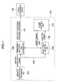
- FIG. 1 is a block diagram showing a configuration of a system provided with a clock supply apparatus according to an embodiment of the present invention.
- the circuits constituting the system shown in Fig. 1 are implemented in the form of CMOS-type digital circuits as in the case of the conventional system described hereinbefore by reference to Fig. 2.
- the power consumption must be zero in principle when the clock supply to the circuits is stopped. Further, the power consumption decreases as the rate or frequency of the driving clock becomes lower.
- the system shown in Fig. 1 comprises a clock supply apparatus 110 and a signal processing block 105, wherein the clock supply apparatus 110 is designed for supplying a high-rate clock signal 107 (which may also be referred to as the high-frequency clock signal) to the signal processing system or block 105 to be utilized in the signal processing executed by the processor 105 in the non-sleep mode, while the supply of the high-rate clock signal 107 to the signal processing block 105 is stopped in the sleep mode.
- a high-rate clock signal 107 which may also be referred to as the high-frequency clock signal
- the clock supply apparatus includes a low-rate source clock generating unit 101 for generating a low-rate source clock signal 106 (which may also be referred to as the low-frequency source clock signal).
- a frequency multiplication/division unit 102 is designed for outputting a high-rate clock signal 107 having a frequency suited for the signal processing performed by the signal processing block 105 through frequency multiplication/division processing of the low-rate source clock signal 106 so long as a sleep signal 108 remains non-active.
- the frequency multiplication/division unit 102 stops operation completely to stop outputting the high-rate clock signal 107.
- the signal processing block 105 is designed for executing a signal processing in conformance with the timing given by the high-rate clock signal 107 during the non-sleep period while stopping the operation completely when the supply of the high-rate clock signal 107 for the signal processing is stopped in the sleep mode.
- the clock supply apparatus further includes a sleep time measuring unit 103 for starting a time measurement from the moment when the sleep signal 108 becomes active, to issue a sleep end signal 109 upon lapse of a predetermined time period.
- the period during which the sleep time measuring unit 103 performs the time measurement represents the sleep period with the other period representing the non-sleep period.
- a sleep control unit 104 constituting another part of the clock supply apparatus is in charge of controlling the sleep/non-sleep mode of the signal processing block 105. More specifically, when the signal processing block 105 is to be set to the sleep mode, the sleep signal 108 is made active to stop the supply of the high-rate clock signal 107 to the signal processing block 105. On the other hand, upon detection of the sleep end signal 109, the sleep control unit 104 recognizes or decides the end or termination of the sleep period to make the sleep signal 108 nonactive. At that time point, the supply of the high-rate clock signal 107 to the signal processing block 105 is started again, whereupon operation of the signal processing block 105 is restarted.
- the signal processing block 105 is set to the completely sleeping state because of interruption of the clock supply during the sleep period, as in the case of the conventional apparatus.
- the low-rate source clock generating unit 101 and the sleep time measuring unit 103 of the clock supply apparatus are maintained in the operating state for measuring the sleep time duration.
- the low-rate clock is employed as the source clock, and the high-rate clock for the signal processing is generated through frequency multiplication/division of the source clock.
- the power consumption can be reduced during the sleep period because only the low-rate source clock generating unit and the sleep period measuring unit are maintained in the operating state during the sleep period. Accordingly, when the clock supply apparatus according to the present invention is applied to a cell-driven portable apparatus/instrument or the like, the time period over which the latter can be operated continuously is extended or elongated, to a great advantage.
Abstract
Description
Claims (2)
- A clock supply apparatus, characterized by comprising:low-rate source clock generating means (101) for generating a low-rate source clock signal (106), said low-rate source clock generating means (101) being provided with automatic frequency control means and temperature drift compensating means;frequency multiplication/division means (102) for performing frequency multiplication/division for said low-rate source clock signal (106) to thereby generate a high-rate clock signal (107) for signal processing only during a period in which a sleep signal (108) remains nonactive, said high-rate clock signal (107) for the signal processing having a frequency higher than that of said low-rate source clock signal (106);sleep time measuring means (103) for performing time measurement with said low-rate source clock signal (106) from the moment when said sleep signal (108) becomes active and issuing a sleep end signal (109) upon measurement of a predetermined time period; andsleep control means (104) for changing over said sleep signal between active state and nonactive state in dependence on sleep or non-sleep mode, said sleep control means (104) deciding end of the sleep period in response to said sleep end signal (109).
- A system having a sleep mode, characterized by comprising:wherein said clock supply apparatus includes low-rate source clock generating means (101) for generating a low-rate source clock signal (106), said low-rate source clock generating means (101) being provided with automatic frequency control means and temperature drift compensating means, frequency multiplication/division means (102) for performing frequency multiplication/division for said low-rate source clock signal (106) to thereby generate a high-rate clock signal (107) for signal processing only during a period in which a sleep signal (108) remains nonactive, said high-rate clock signal (107) for the signal processing having a frequency higher than that of said low-rate source clock signal (106), sleep time measuring means (103) for performing time measurement with said low-rate source clock signal (106) from the moment when said sleep signal (108) becomes active and issuing a sleep end signal (109) in response to a predetermined time period, and sleep control means (104) for changing over said sleep signal between active state and nonactive state in dependence on sleep or non-sleep mode, said sleep control means (104) deciding end of the sleep period upon generation of said sleep end signal (109).signal processing block means (105) for which sleep/non-sleep control is performed by a clock supply apparatus,
Applications Claiming Priority (3)
| Application Number | Priority Date | Filing Date | Title |
|---|---|---|---|
| JP11866197A JPH10301661A (en) | 1997-04-23 | 1997-04-23 | Clock supplying device |
| JP11866197 | 1997-04-23 | ||
| JP118661/97 | 1997-04-23 |
Publications (2)
| Publication Number | Publication Date |
|---|---|
| EP0874302A1 true EP0874302A1 (en) | 1998-10-28 |
| EP0874302B1 EP0874302B1 (en) | 2000-11-08 |
Family
ID=14742095
Family Applications (1)
| Application Number | Title | Priority Date | Filing Date |
|---|---|---|---|
| EP98302678A Expired - Lifetime EP0874302B1 (en) | 1997-04-23 | 1998-04-06 | Clock supply apparatus |
Country Status (7)
| Country | Link |
|---|---|
| US (1) | US6064252A (en) |
| EP (1) | EP0874302B1 (en) |
| JP (1) | JPH10301661A (en) |
| KR (1) | KR100303271B1 (en) |
| CN (1) | CN1101566C (en) |
| CA (1) | CA2235252C (en) |
| DE (1) | DE69800385T2 (en) |
Cited By (2)
| Publication number | Priority date | Publication date | Assignee | Title |
|---|---|---|---|---|
| CN107411177A (en) * | 2012-05-14 | 2017-12-01 | 尼科投资控股有限公司 | Electronics steam provides device |
| US11701482B2 (en) | 2012-10-19 | 2023-07-18 | Nicoventures Trading Limited | Electronic inhalation device |
Families Citing this family (10)
| Publication number | Priority date | Publication date | Assignee | Title |
|---|---|---|---|---|
| KR100420116B1 (en) | 2000-08-31 | 2004-03-02 | 삼성전자주식회사 | Circuit and method for generating processor clock for low power consumption cdma modem chip design |
| US7346791B2 (en) * | 2003-03-26 | 2008-03-18 | Matsushita Electric Industrial Co., Ltd. | Method for controlling a clock frequency of an information processor in accordance with the detection of a start and a end of a specific processing section |
| JP2005196877A (en) * | 2004-01-07 | 2005-07-21 | Matsushita Electric Ind Co Ltd | Optical integrated element |
| US7106118B2 (en) * | 2004-01-16 | 2006-09-12 | Realtek Semiconductor Corp. | Clock signal generator with low power comsumption function and method thereof |
| TWI245178B (en) * | 2004-01-16 | 2005-12-11 | Realtek Semiconductor Corp | Clock generation method and apparatus |
| JP4595937B2 (en) * | 2006-12-28 | 2010-12-08 | ソニー株式会社 | Information processing apparatus, information processing method, and program |
| JP4644747B1 (en) * | 2009-11-02 | 2011-03-02 | パナソニック株式会社 | Information processing apparatus, control method, and control program |
| US10664241B2 (en) * | 2017-10-13 | 2020-05-26 | University Of Virginia Patent Foundation | Memory systems including support for transposition operations and related methods and circuits |
| JP7323185B2 (en) * | 2020-04-24 | 2023-08-08 | 深田工業株式会社 | Intrinsically safe explosion-proof detection system |
| CN115826731B (en) * | 2022-10-19 | 2023-07-11 | 科东(广州)软件科技有限公司 | Sleep control method and device, storage medium and computing equipment |
Citations (2)
| Publication number | Priority date | Publication date | Assignee | Title |
|---|---|---|---|---|
| US5546568A (en) * | 1993-12-29 | 1996-08-13 | Intel Corporation | CPU clock control unit |
| US5596765A (en) * | 1994-10-19 | 1997-01-21 | Advanced Micro Devices, Inc. | Integrated processor including a device for multiplexing external pin signals |
Family Cites Families (3)
| Publication number | Priority date | Publication date | Assignee | Title |
|---|---|---|---|---|
| US5428820A (en) * | 1993-10-01 | 1995-06-27 | Motorola | Adaptive radio receiver controller method and apparatus |
| US5845139A (en) * | 1995-06-07 | 1998-12-01 | Advanced Micro Devices, Inc. | System for providing a host computer with access to a memory on a PCMCIA card in a power down mode |
| US5848281A (en) * | 1996-07-23 | 1998-12-08 | Smalley; Kenneth George | Method and apparatus for powder management in a multifunction controller with an embedded microprocessor |
-
1997
- 1997-04-23 JP JP11866197A patent/JPH10301661A/en active Pending
-
1998
- 1998-04-06 DE DE1998600385 patent/DE69800385T2/en not_active Expired - Lifetime
- 1998-04-06 EP EP98302678A patent/EP0874302B1/en not_active Expired - Lifetime
- 1998-04-15 US US09/060,302 patent/US6064252A/en not_active Expired - Lifetime
- 1998-04-21 CA CA 2235252 patent/CA2235252C/en not_active Expired - Fee Related
- 1998-04-22 CN CN98107313A patent/CN1101566C/en not_active Expired - Fee Related
- 1998-04-23 KR KR1019980014523A patent/KR100303271B1/en not_active IP Right Cessation
Patent Citations (2)
| Publication number | Priority date | Publication date | Assignee | Title |
|---|---|---|---|---|
| US5546568A (en) * | 1993-12-29 | 1996-08-13 | Intel Corporation | CPU clock control unit |
| US5596765A (en) * | 1994-10-19 | 1997-01-21 | Advanced Micro Devices, Inc. | Integrated processor including a device for multiplexing external pin signals |
Cited By (4)
| Publication number | Priority date | Publication date | Assignee | Title |
|---|---|---|---|---|
| CN107411177A (en) * | 2012-05-14 | 2017-12-01 | 尼科投资控股有限公司 | Electronics steam provides device |
| US11185649B2 (en) | 2012-05-14 | 2021-11-30 | Nicoventures Trading Limited | Electronic vapor provision device |
| US11931507B2 (en) | 2012-05-14 | 2024-03-19 | Nicoventures Trading Limited | Electronic vapor provision device |
| US11701482B2 (en) | 2012-10-19 | 2023-07-18 | Nicoventures Trading Limited | Electronic inhalation device |
Also Published As
| Publication number | Publication date |
|---|---|
| DE69800385T2 (en) | 2001-04-26 |
| DE69800385D1 (en) | 2000-12-14 |
| US6064252A (en) | 2000-05-16 |
| KR100303271B1 (en) | 2001-09-29 |
| EP0874302B1 (en) | 2000-11-08 |
| CA2235252C (en) | 2000-06-06 |
| JPH10301661A (en) | 1998-11-13 |
| KR19980081669A (en) | 1998-11-25 |
| CA2235252A1 (en) | 1998-10-23 |
| CN1101566C (en) | 2003-02-12 |
| CN1197948A (en) | 1998-11-04 |
Similar Documents
| Publication | Publication Date | Title |
|---|---|---|
| EP0874302B1 (en) | Clock supply apparatus | |
| US5291542A (en) | Mobile telephone having a power-conserving subroutine | |
| US8456136B2 (en) | Method and apparatus for battery gauging in portable terminal | |
| EP0887990B1 (en) | Modem unit | |
| US9261937B2 (en) | Information processing apparatus and power supply control circuit | |
| JP5231047B2 (en) | Control device | |
| US20060236144A1 (en) | Method for saving power of a laptop computer | |
| US8046088B2 (en) | Dependent power supplying apparatus and electronic instrument | |
| JPH10164764A (en) | Battery capacity monitoring method | |
| KR100584324B1 (en) | Apparatus for controlling power in complex mobile terminal | |
| JPH113151A (en) | Hibernation control method for information processor and battery driven electronic equipment | |
| TWI579686B (en) | Electronic device with power controll function | |
| USRE39523E1 (en) | Power control apparatus for a battery-powered communication system | |
| US5799177A (en) | Automatic external clock detect and source select circuit | |
| JP2001350739A (en) | Microcomputer | |
| JPH11259183A (en) | Information processor | |
| JP2002007988A (en) | Pc(personal computer) card | |
| JP2881065B2 (en) | Modem device | |
| JP2007062243A (en) | Printing apparatus | |
| US20050060593A1 (en) | Inquiring apparatus and method thereof | |
| US20040155530A1 (en) | Frequency regulating circuit | |
| JP3935646B2 (en) | Electric vehicle control device | |
| JP3958546B2 (en) | Buffer control system and buffer controllable memory | |
| US6826635B2 (en) | Input/output pad with mornitoring ability and operation method thereof | |
| JP2008220099A (en) | Power supply system and apparatus having the same |
Legal Events
| Date | Code | Title | Description |
|---|---|---|---|
| PUAI | Public reference made under article 153(3) epc to a published international application that has entered the european phase |
Free format text: ORIGINAL CODE: 0009012 |
|
| 17P | Request for examination filed |
Effective date: 19980417 |
|
| AK | Designated contracting states |
Kind code of ref document: A1 Designated state(s): DE FI FR GB SE |
|
| AX | Request for extension of the european patent |
Free format text: AL;LT;LV;MK;RO;SI |
|
| 17Q | First examination report despatched |
Effective date: 19990211 |
|
| AKX | Designation fees paid |
Free format text: DE FI FR GB SE |
|
| GRAG | Despatch of communication of intention to grant |
Free format text: ORIGINAL CODE: EPIDOS AGRA |
|
| GRAG | Despatch of communication of intention to grant |
Free format text: ORIGINAL CODE: EPIDOS AGRA |
|
| GRAH | Despatch of communication of intention to grant a patent |
Free format text: ORIGINAL CODE: EPIDOS IGRA |
|
| GRAH | Despatch of communication of intention to grant a patent |
Free format text: ORIGINAL CODE: EPIDOS IGRA |
|
| GRAA | (expected) grant |
Free format text: ORIGINAL CODE: 0009210 |
|
| AK | Designated contracting states |
Kind code of ref document: B1 Designated state(s): DE FI FR GB SE |
|
| REF | Corresponds to: |
Ref document number: 69800385 Country of ref document: DE Date of ref document: 20001214 |
|
| ET | Fr: translation filed | ||
| RTI2 | Title (correction) |
Free format text: CLOCK SUPPLY APPARATUS |
|
| PLBE | No opposition filed within time limit |
Free format text: ORIGINAL CODE: 0009261 |
|
| STAA | Information on the status of an ep patent application or granted ep patent |
Free format text: STATUS: NO OPPOSITION FILED WITHIN TIME LIMIT |
|
| 26N | No opposition filed | ||
| REG | Reference to a national code |
Ref country code: GB Ref legal event code: IF02 |
|
| PGFP | Annual fee paid to national office [announced via postgrant information from national office to epo] |
Ref country code: GB Payment date: 20130403 Year of fee payment: 16 Ref country code: SE Payment date: 20130412 Year of fee payment: 16 Ref country code: DE Payment date: 20130403 Year of fee payment: 16 |
|
| PGFP | Annual fee paid to national office [announced via postgrant information from national office to epo] |
Ref country code: FR Payment date: 20130625 Year of fee payment: 16 Ref country code: FI Payment date: 20130410 Year of fee payment: 16 |
|
| REG | Reference to a national code |
Ref country code: DE Ref legal event code: R119 Ref document number: 69800385 Country of ref document: DE |
|
| REG | Reference to a national code |
Ref country code: SE Ref legal event code: EUG |
|
| GBPC | Gb: european patent ceased through non-payment of renewal fee |
Effective date: 20140406 |
|
| REG | Reference to a national code |
Ref country code: FR Ref legal event code: ST Effective date: 20141231 |
|
| REG | Reference to a national code |
Ref country code: DE Ref legal event code: R119 Ref document number: 69800385 Country of ref document: DE Effective date: 20141101 |
|
| PG25 | Lapsed in a contracting state [announced via postgrant information from national office to epo] |
Ref country code: FI Free format text: LAPSE BECAUSE OF NON-PAYMENT OF DUE FEES Effective date: 20140406 Ref country code: DE Free format text: LAPSE BECAUSE OF NON-PAYMENT OF DUE FEES Effective date: 20141101 Ref country code: GB Free format text: LAPSE BECAUSE OF NON-PAYMENT OF DUE FEES Effective date: 20140406 Ref country code: SE Free format text: LAPSE BECAUSE OF NON-PAYMENT OF DUE FEES Effective date: 20140407 |
|
| PG25 | Lapsed in a contracting state [announced via postgrant information from national office to epo] |
Ref country code: FR Free format text: LAPSE BECAUSE OF NON-PAYMENT OF DUE FEES Effective date: 20140430 |