EP0854511A2 - Resin sealing type semiconductor device - Google Patents
Resin sealing type semiconductor device Download PDFInfo
- Publication number
- EP0854511A2 EP0854511A2 EP98100152A EP98100152A EP0854511A2 EP 0854511 A2 EP0854511 A2 EP 0854511A2 EP 98100152 A EP98100152 A EP 98100152A EP 98100152 A EP98100152 A EP 98100152A EP 0854511 A2 EP0854511 A2 EP 0854511A2
- Authority
- EP
- European Patent Office
- Prior art keywords
- forming surface
- circuit forming
- semiconductor device
- leads
- type semiconductor
- Prior art date
- Legal status (The legal status is an assumption and is not a legal conclusion. Google has not performed a legal analysis and makes no representation as to the accuracy of the status listed.)
- Granted
Links
Images


Classifications
-
- H—ELECTRICITY
- H01—ELECTRIC ELEMENTS
- H01L—SEMICONDUCTOR DEVICES NOT COVERED BY CLASS H10
- H01L23/00—Details of semiconductor or other solid state devices
- H01L23/28—Encapsulations, e.g. encapsulating layers, coatings, e.g. for protection
-
- H—ELECTRICITY
- H01—ELECTRIC ELEMENTS
- H01L—SEMICONDUCTOR DEVICES NOT COVERED BY CLASS H10
- H01L23/00—Details of semiconductor or other solid state devices
- H01L23/48—Arrangements for conducting electric current to or from the solid state body in operation, e.g. leads, terminal arrangements ; Selection of materials therefor
- H01L23/488—Arrangements for conducting electric current to or from the solid state body in operation, e.g. leads, terminal arrangements ; Selection of materials therefor consisting of soldered or bonded constructions
- H01L23/495—Lead-frames or other flat leads
- H01L23/49503—Lead-frames or other flat leads characterised by the die pad
- H01L23/4951—Chip-on-leads or leads-on-chip techniques, i.e. inner lead fingers being used as die pad
-
- H—ELECTRICITY
- H01—ELECTRIC ELEMENTS
- H01L—SEMICONDUCTOR DEVICES NOT COVERED BY CLASS H10
- H01L23/00—Details of semiconductor or other solid state devices
- H01L23/28—Encapsulations, e.g. encapsulating layers, coatings, e.g. for protection
- H01L23/31—Encapsulations, e.g. encapsulating layers, coatings, e.g. for protection characterised by the arrangement or shape
- H01L23/3107—Encapsulations, e.g. encapsulating layers, coatings, e.g. for protection characterised by the arrangement or shape the device being completely enclosed
- H01L23/3114—Encapsulations, e.g. encapsulating layers, coatings, e.g. for protection characterised by the arrangement or shape the device being completely enclosed the device being a chip scale package, e.g. CSP
-
- H—ELECTRICITY
- H01—ELECTRIC ELEMENTS
- H01L—SEMICONDUCTOR DEVICES NOT COVERED BY CLASS H10
- H01L2224/00—Indexing scheme for arrangements for connecting or disconnecting semiconductor or solid-state bodies and methods related thereto as covered by H01L24/00
- H01L2224/01—Means for bonding being attached to, or being formed on, the surface to be connected, e.g. chip-to-package, die-attach, "first-level" interconnects; Manufacturing methods related thereto
- H01L2224/26—Layer connectors, e.g. plate connectors, solder or adhesive layers; Manufacturing methods related thereto
- H01L2224/31—Structure, shape, material or disposition of the layer connectors after the connecting process
- H01L2224/32—Structure, shape, material or disposition of the layer connectors after the connecting process of an individual layer connector
- H01L2224/321—Disposition
- H01L2224/32151—Disposition the layer connector connecting between a semiconductor or solid-state body and an item not being a semiconductor or solid-state body, e.g. chip-to-substrate, chip-to-passive
- H01L2224/32221—Disposition the layer connector connecting between a semiconductor or solid-state body and an item not being a semiconductor or solid-state body, e.g. chip-to-substrate, chip-to-passive the body and the item being stacked
- H01L2224/32245—Disposition the layer connector connecting between a semiconductor or solid-state body and an item not being a semiconductor or solid-state body, e.g. chip-to-substrate, chip-to-passive the body and the item being stacked the item being metallic
-
- H—ELECTRICITY
- H01—ELECTRIC ELEMENTS
- H01L—SEMICONDUCTOR DEVICES NOT COVERED BY CLASS H10
- H01L2224/00—Indexing scheme for arrangements for connecting or disconnecting semiconductor or solid-state bodies and methods related thereto as covered by H01L24/00
- H01L2224/01—Means for bonding being attached to, or being formed on, the surface to be connected, e.g. chip-to-package, die-attach, "first-level" interconnects; Manufacturing methods related thereto
- H01L2224/42—Wire connectors; Manufacturing methods related thereto
- H01L2224/44—Structure, shape, material or disposition of the wire connectors prior to the connecting process
- H01L2224/45—Structure, shape, material or disposition of the wire connectors prior to the connecting process of an individual wire connector
- H01L2224/45001—Core members of the connector
- H01L2224/45099—Material
- H01L2224/451—Material with a principal constituent of the material being a metal or a metalloid, e.g. boron (B), silicon (Si), germanium (Ge), arsenic (As), antimony (Sb), tellurium (Te) and polonium (Po), and alloys thereof
- H01L2224/45138—Material with a principal constituent of the material being a metal or a metalloid, e.g. boron (B), silicon (Si), germanium (Ge), arsenic (As), antimony (Sb), tellurium (Te) and polonium (Po), and alloys thereof the principal constituent melting at a temperature of greater than or equal to 950°C and less than 1550°C
- H01L2224/45144—Gold (Au) as principal constituent
-
- H—ELECTRICITY
- H01—ELECTRIC ELEMENTS
- H01L—SEMICONDUCTOR DEVICES NOT COVERED BY CLASS H10
- H01L2224/00—Indexing scheme for arrangements for connecting or disconnecting semiconductor or solid-state bodies and methods related thereto as covered by H01L24/00
- H01L2224/01—Means for bonding being attached to, or being formed on, the surface to be connected, e.g. chip-to-package, die-attach, "first-level" interconnects; Manufacturing methods related thereto
- H01L2224/42—Wire connectors; Manufacturing methods related thereto
- H01L2224/47—Structure, shape, material or disposition of the wire connectors after the connecting process
- H01L2224/48—Structure, shape, material or disposition of the wire connectors after the connecting process of an individual wire connector
- H01L2224/4805—Shape
- H01L2224/4809—Loop shape
- H01L2224/48091—Arched
-
- H—ELECTRICITY
- H01—ELECTRIC ELEMENTS
- H01L—SEMICONDUCTOR DEVICES NOT COVERED BY CLASS H10
- H01L2224/00—Indexing scheme for arrangements for connecting or disconnecting semiconductor or solid-state bodies and methods related thereto as covered by H01L24/00
- H01L2224/01—Means for bonding being attached to, or being formed on, the surface to be connected, e.g. chip-to-package, die-attach, "first-level" interconnects; Manufacturing methods related thereto
- H01L2224/42—Wire connectors; Manufacturing methods related thereto
- H01L2224/47—Structure, shape, material or disposition of the wire connectors after the connecting process
- H01L2224/48—Structure, shape, material or disposition of the wire connectors after the connecting process of an individual wire connector
- H01L2224/481—Disposition
- H01L2224/48151—Connecting between a semiconductor or solid-state body and an item not being a semiconductor or solid-state body, e.g. chip-to-substrate, chip-to-passive
- H01L2224/48221—Connecting between a semiconductor or solid-state body and an item not being a semiconductor or solid-state body, e.g. chip-to-substrate, chip-to-passive the body and the item being stacked
- H01L2224/48245—Connecting between a semiconductor or solid-state body and an item not being a semiconductor or solid-state body, e.g. chip-to-substrate, chip-to-passive the body and the item being stacked the item being metallic
- H01L2224/48247—Connecting between a semiconductor or solid-state body and an item not being a semiconductor or solid-state body, e.g. chip-to-substrate, chip-to-passive the body and the item being stacked the item being metallic connecting the wire to a bond pad of the item
-
- H—ELECTRICITY
- H01—ELECTRIC ELEMENTS
- H01L—SEMICONDUCTOR DEVICES NOT COVERED BY CLASS H10
- H01L2224/00—Indexing scheme for arrangements for connecting or disconnecting semiconductor or solid-state bodies and methods related thereto as covered by H01L24/00
- H01L2224/01—Means for bonding being attached to, or being formed on, the surface to be connected, e.g. chip-to-package, die-attach, "first-level" interconnects; Manufacturing methods related thereto
- H01L2224/42—Wire connectors; Manufacturing methods related thereto
- H01L2224/47—Structure, shape, material or disposition of the wire connectors after the connecting process
- H01L2224/48—Structure, shape, material or disposition of the wire connectors after the connecting process of an individual wire connector
- H01L2224/481—Disposition
- H01L2224/48151—Connecting between a semiconductor or solid-state body and an item not being a semiconductor or solid-state body, e.g. chip-to-substrate, chip-to-passive
- H01L2224/48221—Connecting between a semiconductor or solid-state body and an item not being a semiconductor or solid-state body, e.g. chip-to-substrate, chip-to-passive the body and the item being stacked
- H01L2224/48245—Connecting between a semiconductor or solid-state body and an item not being a semiconductor or solid-state body, e.g. chip-to-substrate, chip-to-passive the body and the item being stacked the item being metallic
- H01L2224/4826—Connecting between the body and an opposite side of the item with respect to the body
-
- H—ELECTRICITY
- H01—ELECTRIC ELEMENTS
- H01L—SEMICONDUCTOR DEVICES NOT COVERED BY CLASS H10
- H01L2224/00—Indexing scheme for arrangements for connecting or disconnecting semiconductor or solid-state bodies and methods related thereto as covered by H01L24/00
- H01L2224/01—Means for bonding being attached to, or being formed on, the surface to be connected, e.g. chip-to-package, die-attach, "first-level" interconnects; Manufacturing methods related thereto
- H01L2224/42—Wire connectors; Manufacturing methods related thereto
- H01L2224/47—Structure, shape, material or disposition of the wire connectors after the connecting process
- H01L2224/48—Structure, shape, material or disposition of the wire connectors after the connecting process of an individual wire connector
- H01L2224/484—Connecting portions
- H01L2224/48463—Connecting portions the connecting portion on the bonding area of the semiconductor or solid-state body being a ball bond
- H01L2224/48465—Connecting portions the connecting portion on the bonding area of the semiconductor or solid-state body being a ball bond the other connecting portion not on the bonding area being a wedge bond, i.e. ball-to-wedge, regular stitch
-
- H—ELECTRICITY
- H01—ELECTRIC ELEMENTS
- H01L—SEMICONDUCTOR DEVICES NOT COVERED BY CLASS H10
- H01L2224/00—Indexing scheme for arrangements for connecting or disconnecting semiconductor or solid-state bodies and methods related thereto as covered by H01L24/00
- H01L2224/73—Means for bonding being of different types provided for in two or more of groups H01L2224/10, H01L2224/18, H01L2224/26, H01L2224/34, H01L2224/42, H01L2224/50, H01L2224/63, H01L2224/71
- H01L2224/732—Location after the connecting process
- H01L2224/73201—Location after the connecting process on the same surface
- H01L2224/73215—Layer and wire connectors
-
- H—ELECTRICITY
- H01—ELECTRIC ELEMENTS
- H01L—SEMICONDUCTOR DEVICES NOT COVERED BY CLASS H10
- H01L24/00—Arrangements for connecting or disconnecting semiconductor or solid-state bodies; Methods or apparatus related thereto
- H01L24/01—Means for bonding being attached to, or being formed on, the surface to be connected, e.g. chip-to-package, die-attach, "first-level" interconnects; Manufacturing methods related thereto
- H01L24/42—Wire connectors; Manufacturing methods related thereto
- H01L24/44—Structure, shape, material or disposition of the wire connectors prior to the connecting process
- H01L24/45—Structure, shape, material or disposition of the wire connectors prior to the connecting process of an individual wire connector
-
- H—ELECTRICITY
- H01—ELECTRIC ELEMENTS
- H01L—SEMICONDUCTOR DEVICES NOT COVERED BY CLASS H10
- H01L24/00—Arrangements for connecting or disconnecting semiconductor or solid-state bodies; Methods or apparatus related thereto
- H01L24/01—Means for bonding being attached to, or being formed on, the surface to be connected, e.g. chip-to-package, die-attach, "first-level" interconnects; Manufacturing methods related thereto
- H01L24/42—Wire connectors; Manufacturing methods related thereto
- H01L24/47—Structure, shape, material or disposition of the wire connectors after the connecting process
- H01L24/48—Structure, shape, material or disposition of the wire connectors after the connecting process of an individual wire connector
-
- H—ELECTRICITY
- H01—ELECTRIC ELEMENTS
- H01L—SEMICONDUCTOR DEVICES NOT COVERED BY CLASS H10
- H01L2924/00—Indexing scheme for arrangements or methods for connecting or disconnecting semiconductor or solid-state bodies as covered by H01L24/00
- H01L2924/0001—Technical content checked by a classifier
- H01L2924/00014—Technical content checked by a classifier the subject-matter covered by the group, the symbol of which is combined with the symbol of this group, being disclosed without further technical details
-
- H—ELECTRICITY
- H01—ELECTRIC ELEMENTS
- H01L—SEMICONDUCTOR DEVICES NOT COVERED BY CLASS H10
- H01L2924/00—Indexing scheme for arrangements or methods for connecting or disconnecting semiconductor or solid-state bodies as covered by H01L24/00
- H01L2924/01—Chemical elements
- H01L2924/01078—Platinum [Pt]
-
- H—ELECTRICITY
- H01—ELECTRIC ELEMENTS
- H01L—SEMICONDUCTOR DEVICES NOT COVERED BY CLASS H10
- H01L2924/00—Indexing scheme for arrangements or methods for connecting or disconnecting semiconductor or solid-state bodies as covered by H01L24/00
- H01L2924/01—Chemical elements
- H01L2924/01079—Gold [Au]
-
- H—ELECTRICITY
- H01—ELECTRIC ELEMENTS
- H01L—SEMICONDUCTOR DEVICES NOT COVERED BY CLASS H10
- H01L2924/00—Indexing scheme for arrangements or methods for connecting or disconnecting semiconductor or solid-state bodies as covered by H01L24/00
- H01L2924/06—Polymers
- H01L2924/078—Adhesive characteristics other than chemical
- H01L2924/07802—Adhesive characteristics other than chemical not being an ohmic electrical conductor
-
- H—ELECTRICITY
- H01—ELECTRIC ELEMENTS
- H01L—SEMICONDUCTOR DEVICES NOT COVERED BY CLASS H10
- H01L2924/00—Indexing scheme for arrangements or methods for connecting or disconnecting semiconductor or solid-state bodies as covered by H01L24/00
- H01L2924/10—Details of semiconductor or other solid state devices to be connected
- H01L2924/11—Device type
- H01L2924/14—Integrated circuits
-
- H—ELECTRICITY
- H01—ELECTRIC ELEMENTS
- H01L—SEMICONDUCTOR DEVICES NOT COVERED BY CLASS H10
- H01L2924/00—Indexing scheme for arrangements or methods for connecting or disconnecting semiconductor or solid-state bodies as covered by H01L24/00
- H01L2924/15—Details of package parts other than the semiconductor or other solid state devices to be connected
- H01L2924/151—Die mounting substrate
- H01L2924/153—Connection portion
- H01L2924/1531—Connection portion the connection portion being formed only on the surface of the substrate opposite to the die mounting surface
- H01L2924/15311—Connection portion the connection portion being formed only on the surface of the substrate opposite to the die mounting surface being a ball array, e.g. BGA
-
- H—ELECTRICITY
- H01—ELECTRIC ELEMENTS
- H01L—SEMICONDUCTOR DEVICES NOT COVERED BY CLASS H10
- H01L2924/00—Indexing scheme for arrangements or methods for connecting or disconnecting semiconductor or solid-state bodies as covered by H01L24/00
- H01L2924/15—Details of package parts other than the semiconductor or other solid state devices to be connected
- H01L2924/181—Encapsulation
- H01L2924/1815—Shape
-
- H—ELECTRICITY
- H05—ELECTRIC TECHNIQUES NOT OTHERWISE PROVIDED FOR
- H05K—PRINTED CIRCUITS; CASINGS OR CONSTRUCTIONAL DETAILS OF ELECTRIC APPARATUS; MANUFACTURE OF ASSEMBLAGES OF ELECTRICAL COMPONENTS
- H05K3/00—Apparatus or processes for manufacturing printed circuits
- H05K3/30—Assembling printed circuits with electric components, e.g. with resistor
- H05K3/303—Surface mounted components, e.g. affixing before soldering, aligning means, spacing means
-
- H—ELECTRICITY
- H05—ELECTRIC TECHNIQUES NOT OTHERWISE PROVIDED FOR
- H05K—PRINTED CIRCUITS; CASINGS OR CONSTRUCTIONAL DETAILS OF ELECTRIC APPARATUS; MANUFACTURE OF ASSEMBLAGES OF ELECTRICAL COMPONENTS
- H05K3/00—Apparatus or processes for manufacturing printed circuits
- H05K3/30—Assembling printed circuits with electric components, e.g. with resistor
- H05K3/32—Assembling printed circuits with electric components, e.g. with resistor electrically connecting electric components or wires to printed circuits
- H05K3/34—Assembling printed circuits with electric components, e.g. with resistor electrically connecting electric components or wires to printed circuits by soldering
- H05K3/341—Surface mounted components
- H05K3/3431—Leadless components
- H05K3/3442—Leadless components having edge contacts, e.g. leadless chip capacitors, chip carriers
Definitions
- the present invention relates generally to a semiconductor device and, more particularly, to a structure of the semiconductor device of a resin sealing type known as a chip scale package in which leads are provided within a size of a semiconductor chip.
- a chip scale package has been developed to meet those demands, and is contrived to downsize the whole by accommodating leads connected to a circuit forming surface of a semiconductor chip within a size of the chip as well as to reduce the thickness by forming a sealing resin layer in such a form that a reverse surface to the circuit forming surface is exposed.
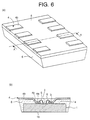
- FIGS. 6(a) and 6(b) are structural views illustrating a resin sealing type semiconductor device of the prior art chip scale package.
- FIG. 6(a) is a perspective view showing an external appearance thereof.
- FIG. 6(b) is an enlarged sectional view taken along the line A-A in FIG. 6(a).
- This semiconductor device includes a semiconductor chip 1, and a plurality of electrodes 2 are formed at a central portion of a circuit forming surface 1a serving as one surface thereof.
- a lead 4 is a thin metal plate crooked at two points.
- the lead 4 has a electrode connecting portion 4a bonded to the circuit forming surface 1a at the central portion of the circuit forming surface 1a through a adhesive tape 3 exhibiting an insulating property, an external connecting portion 4b formed with a step substantially in parallel to the connecting portion 4a, and an inclined middle portion 4c for connecting the electrode connecting portion 4a to the external connecting portion 4b.
- the electrode connecting portion 4a of the lead 4 is electrically connected to the electrode 2 via a metal wire 5.
- the external connecting portion 4b is disposed at a predetermined interval with respect to the circuit forming surface 1a.
- the circuit forming surface 1a of the semiconductor chip 1 and the peripheral side surface are sealed with a sealing resin layer 6 formed by molding in a state where only the external connecting portion 4b of the lead 4 is exposed.
- a reverse surface 1b opposite to the circuit forming surface 1a of the semiconductor chip 1 is not covered with the sealing resin layer 6 and is in a state of being exposed.
- the thus constructed semiconductor device is manufactured by, e.g., the following processes.
- the lead 4 of a molded lead frame is bonded to the circuit forming surface 1a of the semiconductor chip 1 by use of the adhesive tape 3, and thereafter the electrode connecting portion 4a of this lead 4 is electrically connected to the electrode 2 on the semiconductor chip 1 through bonding of the metal wire 5.
- the electrode connecting portion 4a is silver-plated for wire bonding when manufacturing the lead frame.
- the semiconductor chip 1 is mounted into a bottom mold for molding in such a state that the lead frame is bonded.
- the semiconductor chip 1 is mounted so that the reverse surface 1b of the semiconductor chip 1 comes into contact with a bottom portion of the bottom mold for molding while a frame member of the lead frame is positioned in a predetermined place in a frame of the bottom mold.
- the bottom mold into which the semiconductor chip 1 is mounted is covered with a top mold paired with this bottom mold, and a liquid mold resin is poured into the molds from a gate. After the mold resin has been hardened, the semiconductor chip molded by the sealing resin layer 6 is taken out of the molds, and an unnecessary portion of the lead frame is cut off. Then, the external connecting portion 4b of the lead 4 is silver-plated for soldering, thus completing the semiconductor device.
- cream solder is coated by screen printing etc over a foot print on a parts mounting surface of the printed-circuit board. Then, the semiconductor device is mounted so that the external connecting portion 4b of the lead 4 comes into contact with an upper area of the cream solder. The mounted semiconductor device is put into a reflow device and heated at approximately 300°C enough to melt the cream solder, thereby soldering the semiconductor device to the printed-circuit board.
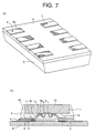
- a first problem is that the mold resin is forced out onto a part of the external connecting portion 4b of the lead 4 of the semiconductor device when in the molding process, resulting in a production of a so-called resin burr 7 illustrated in a perspective view of FIG. 3(a).
- the external connecting portion 4b of the lead 4 comes into a state of floating within a cavity, and there is no contrivance to press it against an internal upper surface of the top mold.
- an adhesion to the top mold is weak, and there might be a high possibility in which the mold resin poured into the molds permeates between the external connecting portion 4b and the internal upper surface of the top mold, thereby producing the resin burr 7.
- the resin burr 7 hinders the semiconductor device from being soldered to the printed-circuit board, and hence there is a necessity for removing the resin burr 7 by a contrivance such as, e.g., flushing the burrs away by high-pressure water before being packaged on the printed-circuit board. This leads to a problem of increasing the number of processes therefor.
- the prior art resin sealing type semiconductor device has a problem of requiring two plating processes with respect to the lead 4 before and after forming the sealing resin layer 6. More specifically, if the resin burr 7 is produced, as described above, the process of removing this burr is needed, and hence the silver plating for soldering, which is effected on the external connecting portion 4b, is required to be executed after the process of removing the resin burr 7. While on the other hand, it is required that the solver plating for wire bonding with respect to the electrode connecting portion 4a be executed when manufacturing the lead frame.
- a second problem is that a crack 11 tends to be caused in the solder 10 for a connection to a foot print 9 on a printed-circuit board 8 as illustrated in FIG. 7(b) showing a packaged state of the semiconductor device on the printed-circuit board.
- the crack is derived from a brittle fracture in the solder 10, which is caused in such a process that if used in an environment where the temperature fluctuates wildly after being packaged on the printed-circuit board, or when cooled down to a normal temperature after being heated by the reflow device, a stress is applied upon the solder 10 due to a difference in terms of thermal expansion coefficient between the sealing resin layer 6 and the printed-circuit board 8. If the crack 11 is produced in the solder 10, there arises a problem in which a mechanical connecting strength between the printed-circuit board 8 and the semiconductor device decreases, and the electrical connection becomes instable.
- a resin sealing type semiconductor device comprises a semiconductor chip including a plurality of electrodes formed at a central portion of a circuit forming surface, and a plurality of leads bonded to the circuit forming surface by a bonding layer having an insulating property, and disposed in a state of being parallel to the circuit forming surface so that their one ends serving as electrode connecting portions are located at the central portion of the circuit forming surface and that their other ends serving as external connecting portions are located at an outer edge of the circuit forming surface.
- This semiconductor device also comprises connecting members for electrically connecting the electrode connecting portions of the plurality of leads to the plurality of electrodes, a sealing resin layer formed by molds so as to cover the plurality of leads, the circuit forming surface and the connecting members in such a state that exposed surfaces of the external connection portions which are opposite to the circuit forming surface are exposed to the outside, and including protruded portions each protruded by one step from the exposed surface at the central portion of the circuit forming surface, and a bump formed on each of the exposed surfaces at a height higher by a fixed dimension than the protruded portion of the sealing resin layer.
- the internal circuit on the semiconductor chip is electrically connected to the bumps through the connecting portions and the leads, and the bumps are connected to the wires of the printed-circuit board, whereby signals can be inputted and outputted to the external circuit disposed on the printed-circuit board.
- the resin sealing type semiconductor device having the above construction is manufactured by sequentially executing a process of bonding the lead by providing a bonding layer in a peripheral portion of the circuit forming surface of the semiconductor chip, a process of respectively electrically connecting the electrode connecting portion of the lead to the electrode on the semiconductor chip through the connecting member, a process of molding the sealing resin layer so as to cover the plurality of leads, the circuit forming surface and the connecting members in such a state that the semiconductor chip with a completion of the above two processes is mounted into the molds for molding, and a surface of the external connecting portion that is opposite to the circuit forming surface is exposed, and a process of forming bumps on the respective exposed surfaces of the plurality of leads.
- the bonding layer may involve the use of an adhesive tape having an insulating property.
- the connecting member may involve the use of a bonding wire.
- the exposed surface of the external connecting portion of the lead may be formed with a recessed portion into which the bump is fixed. In this case, it is desirable that an internal surface of the recessed portion be subjected to metal plating for soldering.
- the bumps may be arranged in one line along a stepped portion defined as a rising portion from the exposed surface of the protruded portion.
- the bumps may be disposed so as to be contiguous to the stepped portion of the sealing resin layer.
- the sealing resin layer is formed so that the stepped portion takes a substantially plane configuration.
- the stepped portions of the sealing resin layer are formed to provide a repetitive layout of recessed and protruded portions so that the areas of the stepped portions which cover the plurality of leads recede toward the central side of the circuit forming surface from other areas.
- a resin sealing type semiconductor device in a state of being fixed to a printed-circuit board, comprises a semiconductor chip including a plurality of electrodes formed at a central portion of a circuit forming surface facing to the printed-circuit board, a plurality of tabular band-like leads electrically connected respectively to the plurality of electrodes, and disposed in a state of being substantially parallel to the circuit forming surface, a sealing resin layer formed so as to cover some portions of the plurality of respective leads and the circuit forming surface, and including protruded portions each so formed as to be contiguous to the printed-circuit board while protruding by one step from the lead at the center of the circuit forming surface, and a plurality of bumps for respectively connecting the exposed surfaces of the leads that are exposed from the sealing resin layer to circuit patterns of the printed-circuit board.
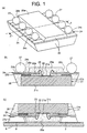
- FIGS. 1(a) and 1(b) are views of a structure of the resin sealing type semiconductor device, showing a first embodiment of the present invention.
- FIG. 1(a) is a perspective view illustrating an external appearance thereof.
- FIG. 1(b) is a sectional view taken along the line A-A in FIG. 1(a).
- the resin sealing type semiconductor device in the first embodiment includes a semiconductor chip 21 assuming a configuration of rectangular parallelopiped, and a plurality of electrodes 22 for connecting an internal circuit of the semiconductor chip 21 to the outside, are formed at the central portion of a circuit forming surface 21a serving as one surface of the chip 21. Totally eight pieces of the electrodes 22 are arranged by fours in two lines in the longitudinal direction of the circuit forming surface 21 in the first embodiment.
- Insulating adhesive tapes 23 which are each approximately 0.8 mm in width, are provided as adhesive layers extending in the longitudinal direction along peripheral portions of the circuit forming surface 21a.
- the adhesive tape 23 is constructed such that both surface of its base composed of, e.g., polyimide which is approximately 50 ⁇ m in thickness are respectively coated with a thermoplastic resin in thickness of approximately 25 ⁇ m.
- a plurality of leads 24 each taking a tabular band-like shape are bonded to the circuit forming surface 21a through these adhesive tapes 23.
- the lead 24 is so provided as to show a one-to-one correspondence to the electrode 22. Accordingly, in this embodiment, totally eight pieces of leads-four leads on each side-are bonded.
- the lead 24 is a lead-out wire for an electrical and mechanical connection when the semiconductor device is packaged on a printed-circuit board, and is a metal plate composed of a material such as, e.g., Fe-Ni alloy etc and having a thickness of approximately 0.1 mm and a width of approximately 1 mm.
- the lead in the embodiment os not protruded long outwardly of the semiconductor chip as in the case of a pin in a prior art flat package etc but is cut to such a length as to be accommodated in the plane of the circuit forming surface 21a in order to downsize the semiconductor device itself.
- the lead 24 is disposed in parallel to the circuit forming surface 21a so that an electrode connecting portion 24a serving as one end thereof is located at the central portion of the circuit forming surface 21a while an external connecting portion serving as the other end thereof is located at an outer edge of the circuit forming surface 21a.
- Metal plating such as silver plating for soldering is effected over the surface (an upper surface in FIG. 1(b))) of the electrode connecting portion 24a, which surface is opposite to the circuit forming surface 21a, whereby the plated portion of the electrode connecting portion 24a is electrically connected to the electrode 22 through a bonding wire (a connecting member) 25 such as a gold wire etc.
- a sealing resin layer 26 composed of epoxy resin etc is formed by molding so as to cover the circuit forming surface 21a and a side surface 21b of the semiconductor chip 21, the bonding wires 25 and the electrode connecting portions 24a.
- An exposed surface 24c, opposite to the circuit forming surface 21a, of the external connecting portion 24b, and a reverse surface 21c opposite to the circuit forming surface 21a of the semiconductor chip 21, are not sealed with the sealing resin layer 26 but are exposed to the outside.
- the sealing resin layer 26 includes a protruded portion 26a protruded by one step from the exposed surface 24c of the lead 24 at the central portion of the circuit forming surface 21a. A rising portion of this protruded portion 26a from the exposed surface 24c of the lead 24, is defined as a stepped portion 26b of the sealing resin layer.
- the stepped portion 26b is formed in a configuration of plane surface.
- the exposed surface 24c of the lead 24 is formed with recessed portions 24x each having a diameter of, e.g., approximately 0.2 mm and a depth of approximately 40 ⁇ m, and internal surface of these recessed portions 24x are metal-plated such as silver plating for soldering.
- Each of the recessed portions 24x of the respective leads 24 is formed with a solder bump 27.
- the solder bump 27 is fixed to the lead 24 at such a height that the solder bump 27 is higher by a fixed dimension than the protruded portion 26a of the sealing resin layer 26 formed covering the circuit forming surface 21a. For example, if a height of the sealing resin layer 26 from the lead 24 is approximately 0.15 mm, the height of the solder bump 27 is approximately 0.5 mm.
- the solder bumps 27 are rectilinearly arranged at a fixed distance from the respective stepped portions 26b of the sealing resin layer 26 on both sides of the protruded portion 26a.
- FIG. 1(c) is a sectional view showing a state of how the resin sealing type semiconductor device in the first embodiment is soldered to a printed-circuit board.
- the protruded portion 26a of the sealing resin layer comes into contact with the printed-circuit board 8, and the lead 24 is electrically connected to a foot print (a circuit pattern) 9 on the printed-circuit board 8 through the solder bump 27a deformed due to the fusion.
- the semiconductor chip 21 is thereby connected to the external circuit via the solder bumps 27, the leads 24 and the boding wired 25, whereby signals are inputted and outputted to the external circuit.
- a lead frame 30 is produced by punching out a metal plate composed of a material such as Fe-Ni alloy etc and having a thickness of approximately 0.1 mm by use of a predetermined pattern.
- the lead frame 30 includes a frame member 31 and a lead portion 32 taking a comb-like shape extending inward from this frame member 31.
- the lead portion 32 assumes such a configuration that when the frame member 31 of the lead frame 30 is cut off, it is left in the form of the lead 24 as shown in FIG. 1. Note that the frame member 31 is formed with a hole 31a for a positioning process simultaneously when punched out with the pattern.
- the recessed portion 24x is formed by etching in the area peripheral to each lead portion 32 on the side of the frame member 31 on one surface 30a of the lead frame 30. Then, the internal surface of the recessed portion 24x and a tip of the lead portion 32 are silver-plated 33 for soldering, thus manufacturing the lead frame 30 as shown in FIG. 2(a).
- FIG. 2 (b) is an explanatory assembly view showing how the semiconductor chip 21 is attached to the lead frame 30.
- the adhesive tape 23 is adhered to the lead portio 32 of a reverse surface 30b opposite to the surface 30a of the lead frame 30. Further, this adhesive tape 23 is thermally crimped to the circuit forming surface 21a of the semiconductor chip 21 at a temperature of approximately 400°C. After the lead frame 30 has been thus bonded to the semiconductor chip 21, the silver plating 33 at the tip of the lead portion 32 is electrically connected to the electrode 22 of the semiconductor chip 21 through the bonding wire 25.
- FIG. 2(c) is an explanatory sectional view showing a mount state of the lead frame 30 into top and bottom molds 41, 42 for a molding process.
- the lead frame 30 fitted with the semiconductor chip is positioned by the hole 31a for a positioning process and mounted in a predetermined position within the top and bottom molds for the molding process.
- the bottom mold 41 is slightly wider in terms of its plane configuration than the circuit forming surface 21a of the semiconductor chip 21, and includes a cavity 41a taking substantially the same configuration. Then, a depth of the cavity 41a is set coincident with a dimension of a sum of thicknesses of the semiconductor chip 21 and of the adhesive tape 23.
- the top mold 42 paired with the bottom mold 41 is covered in a predetermined position of the bottom mold 41.
- the top mold 42 is formed with a cavity 42a having an aperture a width of which is narrower than the aperture of the cavity 41a of the bottom mold 41, and a plane base member 42 is formed along the periphery of the cavity 42a.
- a depth of the cavity 42a of the top mold 42 is set larger than a protrusion quantity of the bonding wire 25 from the surface 30a of the lead from 30.
- the top and bottom molds 41, 42 are matched by a predetermined pressure, at which time the reverse surface 21c of the semiconductor chip 21 to which the adhesive tape 23 is adhered comes into contact with the bottom surface of the cavity 41a of the bottom mold 41, and the lead portion 32 of the lead frame 30 comes into contact with the base member or of the top mold 42. Then, a bonding portion between the lead portion 32 and the adhesive tape 23 is fixed in a state of its being sandwiched in between the top and bottom molds 41, 42.
- the whack chip 21, to which the lead frame 30 is bonded is mounted into the top and bottom molds 41, 42, and a mold resin such as epoxy resin molten into a liquid is poured from a gate into the cavities 41a, 42a.
- the semiconductor chip 21 molded by the sealing resin layer 26 is taken out, and an unnecessary portion of the lead frame 30 is cut off. Then, the flux for soldering is coated over the recessed portion 24x formed in the exposed surface 24c of the lead 24, and the solder ball having the diameter of approximately 0.5 mm is mounted thereon, wherein a reflow process is executed at, e.g., 240°C. The solder bump 27 is thereby formed in the recessed portion 24x, and the resin sealing type semiconductor device as shown in FIG. 1(a) is completed.
- the resin sealing type semiconductor device in the first embodiment exhibits the following advantages (i) - (v) owing to the construction described above.
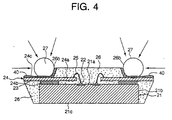
- FIGS. 3(a) and 3(b) are sectional views illustrating a second embodiment of the resin sealing type semiconductor device according to the present invention.
- FIG. 3 (a) is a perspective view of the whole.
- FIG. 3(b) is a sectional view taken along the line A-A in FIG. 3(a), showing only the right part in FIG. 3(a).
- the stepped portion 26b of the sealing resin layer 26 is formed in a substantially planar shape, and the solder bump 27 is fixed onto the exposed surface 24c of the lead 24 in a state of being in contact with the stepped portion 26b.
- the construction of the semiconductor device in the second embodiment is the same as that in the first embodiment except for the fixing position of the solder bump 27. Though an illustration is omitted, in the semiconductor device in accordance with the second embodiment too, the solder bumps 27 are rectilinearly arranged in two lines along the stepped portion 26b.
- solder bumps 27 When forming the solder bumps 27 respectively on the plurality of leads 24, and if trying to form the solder bumps 27 on middle portions of the exposed surfaces 24c of the leads 24, it is difficult to position the solder bumps 27 in order to attain the rectilinear arrangement of the solder bumps 27.
- the solder bumps 27 when the solder bumps 27 are arranged along the stepped portion 26b, the solder bumps 27 can be easily rectilinearly arranged.
- the solder ball is disposed on the liquid flux coated over the exposed surface 24c of the lead 24, and therefore, if the solder balls are disposed on the middle portions of the exposed surfaces 24c, the solder balls are easy to move, with the result that it is impossible to rectilinearly arrange and fix the plurality of solder bumps 27.
- the solder bumps 27 are, as in the second embodiment, arranged along the stepped portion 26b, before the solder bumps 27 are fixed, a flux 40 is coated over not only the exposed surfaces of the leads 24 but also the stepped portion 26b of the sealing resin layer 26, whereby the solder bumps 27 are, as shown in FIG.
- FIGS. 5(a) and 5(b) show a third embodiment of the resin sealing type semiconductor device according to the present invention.
- FIG. 5(a) is a plan view.
- FIG. 5(b) is a sectional view taken along the line A-A in FIG. 5(a).
- stepped portions 26e of the sealing resin layer 26 are, as illustrated in FIG. 5(a), formed in such a configuration as to provide a repetitive layout of recessed portions 26f and protruded portions 26g so that areas covering the leads 24 recede toward the central side (a left side in the Figure) of the circuit forming surface 21a from other areas.
- the solder bump 27 is fixed in such a position as to come into the contact with angular portions of the protruded portions 26 on both sides in a state of being fitted into a part of the recessed portion 26f.
- the plurality of solder bumps 27 can be precisely rectilinearly arranged and fixed. Note that the respective embodiments discussed above have a smaller possibility of causing the resin burr than in the prior arts, however, it might happen that the resin burr is produced due to some inconvenience of being mounted into the molds. There is a high probability that the resin burr is produced in close proximity to the sealing resin layer 26 of the lead 24, and hence, as in the second embodiment, if the solder bump 27 is fixed in contact with the stepped portion 26b, there might be a possibility in which the resin burr hinders the fixation of the solder bump 27.
- the recessed portion 26f is formed in the portion covering the lead 24, even if a resin burr 41 is produced, a possibility of this resin burr 41 reaching the fixing position of the solder bump 27, is small. If the resin burr 41 is produced on the lead 24 too, the solder bump 27 can be fixed without going through the step of removing the resin burr 41.
- the lead takes the tabular band-like shape with no stepped portion unlike the prior art, and therefore the lead frame is easy to manufacture. Besides, since a distance between the lead the semiconductor chip does not change depending on the positions of the respective portions within the lead, it is easy to firmly fix the lead to the semiconductor chip, and the adhesion between the exposed surface of the lead and the mold is enhanced, whereby the occurrence of the resin burr can be readily avoided.
- the bump is provided higher than the protruded portion of the sealing resin layer, and therefore has the larger thickness than in the prior art. Then, there is dispersed the stress due to the change in temperature after being packaged on the printed-circuit board, and it is feasible to restrain the cracks from being produced in the bumps.
- the reverse surface of the semiconductor chip that is opposite to the circuit forming surface is not covered with the sealing resin layer and is exposed to the outside, in which case the heat evolved on the semiconductor chip can be readily radiated. Further, in this case, the semiconductor comes into contact with the bottom surface of one mold when mounted into the molds, and hence the leads bonded to the circuit forming surface can be supported more surely, thereby making it feasible to prevent the resin from permeating between the other mold and the exposed surface of the lead.
- the bumps may be, when fixed, disposed along the protruded portion of the sealing resin layer, which facilitates the positioning process of each bump and makes it possible to readily rectilinearly arrange the plurality of bumps.
- the area of the stepped portion that covers the lead is so formed as to recede toward the central side of the circuit forming surface from other areas, the area in which the resin burr tends to occur can be set apart from the bump fixing portion. Even if the resin burr is produced, the bump can be fixed without removing the burr.
Abstract
Description
- 21
- SEMICONDUCTOR CHIP
- 22
- ELECTRODE
- 23
- ADHESIVE TAPE
- 24
- LEAD
- 24a
- ELECTRODE CONNECTING PORTION
- 24b
- EXTERNAL CONNECTING PORTION
- 24c
- EXPOSED SURFACE
- 25
- BONDING WIRE
- 26
- SEALING RESIN LAYER
- 26a
- PROTRUDED PORTION
- 26b
- STEPPED PORTION
Claims (13)
- A resin sealing type semiconductor device comprising:a semiconductor chip including a plurality of electrodes formed at a central portion of a circuit forming surface;a plurality of leads bonded to said circuit forming surface by a bonding layer having an insulating property, and disposed in a state of being parallel to said circuit forming surface so that their one ends serving as electrode connecting portions are located at the central portion of said circuit forming surface and that their other ends serving as external connecting portions are located at an outer edge of said circuit forming surface;connecting means for electrically connecting said electrode connecting portions of said plurality of leads to said plurality of electrodes;a sealing resin layer formed by molds so as to cover said plurality of leads, said circuit forming surface and said connecting means in such a state that exposed surfaces of said external connection portions which are opposite to said circuit forming surface are exposed to the outside, and including protruded portions each protruded by one step from said exposed surface at the central portion of said circuit forming surface; anda bump formed on each of said exposed surfaces.
- A resin sealing type semiconductor device according to claim 1, wherein said bonding layer is an adhesive tape having an insulating property, and said connecting means is a bonding wire.
- A resin sealing type semiconductor device according to any one of claims 1 and 2, wherein said exposed surface of said external connecting portion is formed with a recessed portion into which said bump is fixed, and an internal surface of said recessed portion is subjected to metal plating for soldering.
- A resin sealing type semiconductor device comprising:a semiconductor chip including a plurality of electrodes formed at a central portion of a circuit forming surface;a plurality of tabular band-like leads electrically connected respectively to said plurality of electrodes, and disposed in a state of being substantially parallel to said circuit forming surface;a sealing resin layer formed so as to cover some portions of said plurality of respective leads and said circuit forming surface, and including protruded portions each so formed as to protrude by one step from said lead at the center of said circuit forming surface; anda plurality of bumps formed respectively on said exposed surfaces of said leads that are exposed from said sealing resin layer.
- A resin sealing type semiconductor device according to any one of claims 1 through 4, wherein said bump is formed on said exposed surface at a height higher by a fixed dimension than said protruded portion.
- A resin sealing type semiconductor device according to any one of claims 1 through 5, wherein a reverse surface of said semiconductor chip that is opposite to said circuit forming surface, is exposed to the outside without being covered with said sealing resin layer.
- A resin sealing type semiconductor device according to any one of claims 1 through 6, wherein said bumps are rectilinearly arranged along a stepped portion defined as a rising portion from said exposed surface of said protruded portion.
- A resin sealing type semiconductor device according to claim 7, wherein said bumps are so disposed as to be contiguous to said stepped portion.
- A resin sealing type semiconductor device according to claim 8, wherein said stepped portion of said sealing resin layer is formed in a substantially plane shape.
- A resin sealing type semiconductor device according to claim 8, wherein said stepped portion of said sealing resin layer is forme din such a configuration as to provide a repetitive layout of recessed and protruded portions so that areas of said stepped portions which cover said plurality of leads recede toward the central side of said circuit forming surface from other areas.
- A resin sealing type semiconductor device fixed on a printed-circuit board, comprising:a semiconductor chip including a plurality of electrodes formed at a central portion of a circuit forming surface facing to said printed-circuit board;a plurality of tabular band-like leads electrically connected respectively to said plurality of electrodes, and disposed in a state of being substantially parallel to said circuit forming surface;a sealing resin layer formed so as to cover some portions of said plurality of respective leads and said circuit forming surface, and including protruded portions each so formed as to be contiguous to said printed-circuit board while protruding by one step from said lead at the center of said circuit forming surface; anda plurality of bumps for respectively connecting said exposed surfaces of said leads that are exposed from said sealing resin layer to circuit patterns of said printed-circuit board.
- A resin sealing type semiconductor device according to claim 11, wherein said leads are bonded to said circuit forming surface through bonding layers exhibiting an insulating property so that their one ends serving as electrode connecting portions are located at the central portion of said circuit forming surface and that their other ends serving as external connecting portions are located at an outer edge of said circuit forming surface.
- A resin sealing type semiconductor device comprising:a semiconductor chip having a plurality of electrodes formed at a circuit forming surface;a plurality of leads fixed over the chip, eah leads having one end for electrically connecting the electrodes and other end;a sealing resin to cover said one end of the leads and said electrodes;a plurality of bump formed on said other end of the leads.
Applications Claiming Priority (6)
| Application Number | Priority Date | Filing Date | Title |
|---|---|---|---|
| JP751997 | 1997-01-20 | ||
| JP7519/97 | 1997-01-20 | ||
| JP751997 | 1997-01-20 | ||
| JP27439297 | 1997-10-07 | ||
| JP27439297A JP3793628B2 (en) | 1997-01-20 | 1997-10-07 | Resin-sealed semiconductor device |
| JP274392/97 | 1997-10-07 |
Publications (3)
| Publication Number | Publication Date |
|---|---|
| EP0854511A2 true EP0854511A2 (en) | 1998-07-22 |
| EP0854511A3 EP0854511A3 (en) | 2000-04-26 |
| EP0854511B1 EP0854511B1 (en) | 2009-07-08 |
Family
ID=26341823
Family Applications (1)
| Application Number | Title | Priority Date | Filing Date |
|---|---|---|---|
| EP98100152A Expired - Lifetime EP0854511B1 (en) | 1997-01-20 | 1998-01-07 | Resin sealing type semiconductor device |
Country Status (6)
| Country | Link |
|---|---|
| US (1) | US5999413A (en) |
| EP (1) | EP0854511B1 (en) |
| JP (1) | JP3793628B2 (en) |
| KR (1) | KR100480543B1 (en) |
| DE (1) | DE69840953D1 (en) |
| TW (1) | TW388974B (en) |
Cited By (2)
| Publication number | Priority date | Publication date | Assignee | Title |
|---|---|---|---|---|
| EP1189279A1 (en) * | 2000-03-13 | 2002-03-20 | Dai Nippon Printing Co., Ltd. | Resin-sealed semiconductor device, circuit member used for the device, and method of manufacturing the circuit member |
| US7704801B2 (en) * | 1999-12-27 | 2010-04-27 | Oki Semiconductor Co., Ltd. | Resin for sealing semiconductor device, resin-sealed semiconductor device and the method of manufacturing the semiconductor device |
Families Citing this family (37)
| Publication number | Priority date | Publication date | Assignee | Title |
|---|---|---|---|---|
| US6165819A (en) * | 1992-10-20 | 2000-12-26 | Fujitsu Limited | Semiconductor device, method of producing semiconductor device and semiconductor device mounting structure |
| JP3638750B2 (en) * | 1997-03-25 | 2005-04-13 | 株式会社ルネサステクノロジ | Semiconductor device |
| JP2954110B2 (en) * | 1997-09-26 | 1999-09-27 | 九州日本電気株式会社 | CSP type semiconductor device and manufacturing method thereof |
| JPH11284007A (en) * | 1998-03-31 | 1999-10-15 | Toshiba Corp | Semiconductor device and manufacture thereof |
| JP2000156435A (en) | 1998-06-22 | 2000-06-06 | Fujitsu Ltd | Semiconductor device and manufacture thereof |
| TW411537B (en) * | 1998-07-31 | 2000-11-11 | Siliconware Precision Industries Co Ltd | Semiconductor package with CSP-BGA structure |
| JP3171176B2 (en) * | 1998-12-15 | 2001-05-28 | 日本電気株式会社 | Semiconductor device and ball grid array manufacturing method |
| KR100299384B1 (en) * | 1998-12-16 | 2001-10-29 | 박종섭 | Ball grid array package |
| JP3169919B2 (en) * | 1998-12-21 | 2001-05-28 | 九州日本電気株式会社 | Ball grid array type semiconductor device and method of manufacturing the same |
| US6541872B1 (en) | 1999-01-11 | 2003-04-01 | Micron Technology, Inc. | Multi-layered adhesive for attaching a semiconductor die to a substrate |
| US6387732B1 (en) * | 1999-06-18 | 2002-05-14 | Micron Technology, Inc. | Methods of attaching a semiconductor chip to a leadframe with a footprint of about the same size as the chip and packages formed thereby |
| US6150730A (en) * | 1999-07-08 | 2000-11-21 | Advanced Semiconductor Engineering, Inc. | Chip-scale semiconductor package |
| JP2001024027A (en) * | 1999-07-09 | 2001-01-26 | Oki Electric Ind Co Ltd | Semiconductor element, manufacture thereof, semiconductor device and manufacture |
| US6534861B1 (en) * | 1999-11-15 | 2003-03-18 | Substrate Technologies Incorporated | Ball grid substrate for lead-on-chip semiconductor package |
| JP3501281B2 (en) * | 1999-11-15 | 2004-03-02 | 沖電気工業株式会社 | Semiconductor device |
| US7019410B1 (en) * | 1999-12-21 | 2006-03-28 | Micron Technology, Inc. | Die attach material for TBGA or flexible circuitry |
| JP2001339011A (en) * | 2000-03-24 | 2001-12-07 | Shinko Electric Ind Co Ltd | Semiconductor device and its manufacturing method |
| US6531335B1 (en) | 2000-04-28 | 2003-03-11 | Micron Technology, Inc. | Interposers including upwardly protruding dams, semiconductor device assemblies including the interposers, and methods |
| KR20020000012A (en) * | 2000-06-20 | 2002-01-04 | 윤종용 | Method for manufacturing chip scale package having slits |
| KR100608608B1 (en) * | 2000-06-23 | 2006-08-09 | 삼성전자주식회사 | Semiconductor chip package having bonding pad structure of mixing type and manufacturing method thereof |
| JP4555436B2 (en) * | 2000-06-29 | 2010-09-29 | 富士通株式会社 | Resin molding method for thin film resin substrate and high frequency module |
| US6762502B1 (en) * | 2000-08-31 | 2004-07-13 | Micron Technology, Inc. | Semiconductor device packages including a plurality of layers substantially encapsulating leads thereof |
| JP3405456B2 (en) | 2000-09-11 | 2003-05-12 | 沖電気工業株式会社 | Semiconductor device, method of manufacturing semiconductor device, stack type semiconductor device, and method of manufacturing stack type semiconductor device |
| US6657298B1 (en) * | 2001-07-18 | 2003-12-02 | Amkor Technology, Inc. | Integrated circuit chip package having an internal lead |
| JP3418385B2 (en) * | 2001-08-10 | 2003-06-23 | 沖電気工業株式会社 | Method of forming semiconductor integrated circuit package and method of manufacturing the same |
| US6921860B2 (en) | 2003-03-18 | 2005-07-26 | Micron Technology, Inc. | Microelectronic component assemblies having exposed contacts |
| US20070132111A1 (en) * | 2004-10-07 | 2007-06-14 | Optimum Care International Tech. Inc. | Fine-sized chip package structure |
| TWI256092B (en) * | 2004-12-02 | 2006-06-01 | Siliconware Precision Industries Co Ltd | Semiconductor package and fabrication method thereof |
| US7745944B2 (en) | 2005-08-31 | 2010-06-29 | Micron Technology, Inc. | Microelectronic devices having intermediate contacts for connection to interposer substrates, and associated methods of packaging microelectronic devices with intermediate contacts |
| JP4698387B2 (en) * | 2005-11-04 | 2011-06-08 | エルピーダメモリ株式会社 | Semiconductor device and manufacturing method thereof |
| DE102006003931B3 (en) * | 2006-01-26 | 2007-08-02 | Infineon Technologies Ag | Semiconductor device with external surface mount contacts and method of making the same |
| JP5353153B2 (en) * | 2007-11-09 | 2013-11-27 | パナソニック株式会社 | Mounting structure |
| FI125526B (en) * | 2008-08-25 | 2015-11-13 | Ge Embedded Electronics Oy | Packaged Circuit Board Structure with Electronic Components and Method for Manufacture of Packaged Circuit Board Structure with Electronic Components |
| US8072770B2 (en) * | 2008-10-14 | 2011-12-06 | Texas Instruments Incorporated | Semiconductor package with a mold material encapsulating a chip and a portion of a lead frame |
| JP5755186B2 (en) | 2012-06-25 | 2015-07-29 | 三菱電機株式会社 | Semiconductor device manufacturing method and semiconductor device |
| JP2015195389A (en) * | 2015-06-17 | 2015-11-05 | 大日本印刷株式会社 | Semiconductor device and manufacturing method thereof |
| KR102157041B1 (en) | 2019-05-03 | 2020-09-18 | (주)신영화학 | Lipstick |
Citations (3)
| Publication number | Priority date | Publication date | Assignee | Title |
|---|---|---|---|---|
| JPH07321244A (en) | 1994-05-27 | 1995-12-08 | Matsushita Electric Ind Co Ltd | Electronic part, and manufacture of electronic part |
| JPH08236586A (en) | 1994-12-29 | 1996-09-13 | Nitto Denko Corp | Semiconductor device and manufacturing method thereof |
| WO1997001865A1 (en) | 1995-06-28 | 1997-01-16 | Hitachi, Ltd. | Semiconductor device and method of manufacturing the same |
Family Cites Families (15)
| Publication number | Priority date | Publication date | Assignee | Title |
|---|---|---|---|---|
| US5200362A (en) * | 1989-09-06 | 1993-04-06 | Motorola, Inc. | Method of attaching conductive traces to an encapsulated semiconductor die using a removable transfer film |
| US5045921A (en) * | 1989-12-26 | 1991-09-03 | Motorola, Inc. | Pad array carrier IC device using flexible tape |
| US5222014A (en) * | 1992-03-02 | 1993-06-22 | Motorola, Inc. | Three-dimensional multi-chip pad array carrier |
| US5474958A (en) * | 1993-05-04 | 1995-12-12 | Motorola, Inc. | Method for making semiconductor device having no die supporting surface |
| US5991156A (en) * | 1993-12-20 | 1999-11-23 | Stmicroelectronics, Inc. | Ball grid array integrated circuit package with high thermal conductivity |
| US5384689A (en) * | 1993-12-20 | 1995-01-24 | Shen; Ming-Tung | Integrated circuit chip including superimposed upper and lower printed circuit boards |
| JP3150253B2 (en) * | 1994-07-22 | 2001-03-26 | 三菱電機株式会社 | Semiconductor device, its manufacturing method and mounting method |
| EP0704896B1 (en) * | 1994-09-22 | 2003-03-26 | Nec Corporation | Tape automated bonding type semiconductor device |
| US5541450A (en) * | 1994-11-02 | 1996-07-30 | Motorola, Inc. | Low-profile ball-grid array semiconductor package |
| US5572066A (en) * | 1995-01-03 | 1996-11-05 | Motorola Inc. | Lead-on-chip semiconductor device and method for its fabrication |
| US5677566A (en) * | 1995-05-08 | 1997-10-14 | Micron Technology, Inc. | Semiconductor chip package |
| JPH0917910A (en) * | 1995-06-28 | 1997-01-17 | Hitachi Ltd | Semiconductor device and its manufacture, inspection method and mounting board |
| JP2894254B2 (en) * | 1995-09-20 | 1999-05-24 | ソニー株式会社 | Semiconductor package manufacturing method |
| KR0184076B1 (en) * | 1995-11-28 | 1999-03-20 | 김광호 | Three-dimensional stacked package |
| MY128748A (en) * | 1995-12-19 | 2007-02-28 | Texas Instruments Inc | Plastic packaging for a surface mounted integrated circuit |
-
1997
- 1997-10-07 JP JP27439297A patent/JP3793628B2/en not_active Expired - Fee Related
- 1997-12-15 US US08/990,790 patent/US5999413A/en not_active Expired - Lifetime
- 1997-12-19 TW TW086119303A patent/TW388974B/en not_active IP Right Cessation
- 1997-12-29 KR KR1019970076812A patent/KR100480543B1/en not_active IP Right Cessation
-
1998
- 1998-01-07 EP EP98100152A patent/EP0854511B1/en not_active Expired - Lifetime
- 1998-01-07 DE DE69840953T patent/DE69840953D1/en not_active Expired - Fee Related
Patent Citations (3)
| Publication number | Priority date | Publication date | Assignee | Title |
|---|---|---|---|---|
| JPH07321244A (en) | 1994-05-27 | 1995-12-08 | Matsushita Electric Ind Co Ltd | Electronic part, and manufacture of electronic part |
| JPH08236586A (en) | 1994-12-29 | 1996-09-13 | Nitto Denko Corp | Semiconductor device and manufacturing method thereof |
| WO1997001865A1 (en) | 1995-06-28 | 1997-01-16 | Hitachi, Ltd. | Semiconductor device and method of manufacturing the same |
Cited By (4)
| Publication number | Priority date | Publication date | Assignee | Title |
|---|---|---|---|---|
| US7704801B2 (en) * | 1999-12-27 | 2010-04-27 | Oki Semiconductor Co., Ltd. | Resin for sealing semiconductor device, resin-sealed semiconductor device and the method of manufacturing the semiconductor device |
| EP1189279A1 (en) * | 2000-03-13 | 2002-03-20 | Dai Nippon Printing Co., Ltd. | Resin-sealed semiconductor device, circuit member used for the device, and method of manufacturing the circuit member |
| EP1189279A4 (en) * | 2000-03-13 | 2006-04-12 | Dainippon Printing Co Ltd | Resin-sealed semiconductor device, circuit member used for the device, and method of manufacturing the circuit member |
| US7307347B2 (en) | 2000-03-13 | 2007-12-11 | Dai Nippon Printing Co., Ltd. | Resin-encapsulated package, lead member for the same and method of fabricating the lead member |
Also Published As
| Publication number | Publication date |
|---|---|
| EP0854511A3 (en) | 2000-04-26 |
| US5999413A (en) | 1999-12-07 |
| JP3793628B2 (en) | 2006-07-05 |
| DE69840953D1 (en) | 2009-08-20 |
| KR100480543B1 (en) | 2005-06-16 |
| JPH10261753A (en) | 1998-09-29 |
| TW388974B (en) | 2000-05-01 |
| KR19980070254A (en) | 1998-10-26 |
| EP0854511B1 (en) | 2009-07-08 |
Similar Documents
| Publication | Publication Date | Title |
|---|---|---|
| EP0854511B1 (en) | Resin sealing type semiconductor device | |
| KR0174761B1 (en) | Flat-card shaped electronic module | |
| US5444301A (en) | Semiconductor package and method for manufacturing the same | |
| US5686361A (en) | Method for manufacturing a semiconductor device having a heat radiator | |
| US6861734B2 (en) | Resin-molded semiconductor device | |
| US5612259A (en) | Method for manufacturing a semiconductor device wherein a semiconductor chip is mounted on a lead frame | |
| JP3201353B2 (en) | Semiconductor device and manufacturing method thereof | |
| US5780933A (en) | Substrate for semiconductor device and semiconductor device using the same | |
| US20070193027A1 (en) | Method of manufacturing circuit device | |
| US20030209815A1 (en) | Semiconductor device and its manufacturing method | |
| KR100389230B1 (en) | Individual semiconductor device and its manufacturing method | |
| KR920000076B1 (en) | Semiconductor device | |
| US20050110127A1 (en) | Semiconductor device | |
| US6323551B1 (en) | Resin sealed-type semiconductor device and method of manufacturing the same | |
| KR20030076199A (en) | Semiconductor Device and Method of Manufacturing the Same | |
| KR20040014178A (en) | A semiconductor device and a method of manufacturing the same | |
| US20020022304A1 (en) | Semiconductor device, method for fabricating the same, circuit board and electronic device | |
| US5382546A (en) | Semiconductor device and method of fabricating same, as well as lead frame used therein and method of fabricating same | |
| JP2006279088A (en) | Method for manufacturing semiconductor device | |
| JPH11186481A (en) | Lead frame | |
| US6022763A (en) | Substrate for semiconductor device, semiconductor device using the same, and method for manufacture thereof | |
| JP2644194B2 (en) | Semiconductor device and manufacturing method thereof | |
| JPH07211847A (en) | Semiconductor device, its manufacture, its mounting structure and mounting method | |
| JP2003179187A (en) | Production method of semiconductor device and packaging method of semiconductor device | |
| JP2536568B2 (en) | Lead frame |
Legal Events
| Date | Code | Title | Description |
|---|---|---|---|
| PUAI | Public reference made under article 153(3) epc to a published international application that has entered the european phase |
Free format text: ORIGINAL CODE: 0009012 |
|
| AK | Designated contracting states |
Kind code of ref document: A2 Designated state(s): DE FR GB NL |
|
| AX | Request for extension of the european patent |
Free format text: AL;LT;LV;MK;RO;SI |
|
| PUAL | Search report despatched |
Free format text: ORIGINAL CODE: 0009013 |
|
| AK | Designated contracting states |
Kind code of ref document: A3 Designated state(s): AT BE CH DE DK ES FI FR GB GR IE IT LI LU MC NL PT SE |
|
| AX | Request for extension of the european patent |
Free format text: AL;LT;LV;MK;RO;SI |
|
| 17P | Request for examination filed |
Effective date: 20000727 |
|
| AKX | Designation fees paid |
Free format text: DE FR GB NL |
|
| 17Q | First examination report despatched |
Effective date: 20030718 |
|
| 17Q | First examination report despatched |
Effective date: 20030718 |
|
| GRAP | Despatch of communication of intention to grant a patent |
Free format text: ORIGINAL CODE: EPIDOSNIGR1 |
|
| GRAS | Grant fee paid |
Free format text: ORIGINAL CODE: EPIDOSNIGR3 |
|
| GRAA | (expected) grant |
Free format text: ORIGINAL CODE: 0009210 |
|
| AK | Designated contracting states |
Kind code of ref document: B1 Designated state(s): DE FR GB NL |
|
| REG | Reference to a national code |
Ref country code: GB Ref legal event code: FG4D |
|
| REF | Corresponds to: |
Ref document number: 69840953 Country of ref document: DE Date of ref document: 20090820 Kind code of ref document: P |
|
| NLV1 | Nl: lapsed or annulled due to failure to fulfill the requirements of art. 29p and 29m of the patents act | ||
| PG25 | Lapsed in a contracting state [announced via postgrant information from national office to epo] |
Ref country code: NL Free format text: LAPSE BECAUSE OF FAILURE TO SUBMIT A TRANSLATION OF THE DESCRIPTION OR TO PAY THE FEE WITHIN THE PRESCRIBED TIME-LIMIT Effective date: 20090708 |
|
| PLBE | No opposition filed within time limit |
Free format text: ORIGINAL CODE: 0009261 |
|
| STAA | Information on the status of an ep patent application or granted ep patent |
Free format text: STATUS: NO OPPOSITION FILED WITHIN TIME LIMIT |
|
| 26N | No opposition filed |
Effective date: 20100409 |
|
| REG | Reference to a national code |
Ref country code: FR Ref legal event code: ST Effective date: 20100930 |
|
| PG25 | Lapsed in a contracting state [announced via postgrant information from national office to epo] |
Ref country code: FR Free format text: LAPSE BECAUSE OF NON-PAYMENT OF DUE FEES Effective date: 20100201 |
|
| PG25 | Lapsed in a contracting state [announced via postgrant information from national office to epo] |
Ref country code: DE Free format text: LAPSE BECAUSE OF NON-PAYMENT OF DUE FEES Effective date: 20100803 |
|
| PGFP | Annual fee paid to national office [announced via postgrant information from national office to epo] |
Ref country code: GB Payment date: 20110105 Year of fee payment: 14 |
|
| GBPC | Gb: european patent ceased through non-payment of renewal fee |
Effective date: 20120107 |
|
| PG25 | Lapsed in a contracting state [announced via postgrant information from national office to epo] |
Ref country code: GB Free format text: LAPSE BECAUSE OF NON-PAYMENT OF DUE FEES Effective date: 20120107 |