Background of the Invention
The present invention relates to photolithography techniques. More particularly,
the invention relates to improved methods and apparatuses for performing optical
proximity correction.
The minimum feature sizes of integrated circuits (ICs) have been shrinking for
years. Commensurate with this size reduction, various process limitations have made
IC fabrication more difficult. One area of fabrication technology in which such
limitations have appeared is photolithography.
Photolithography involves selectively exposing regions of a resist coated silicon
wafer to a radiation pattern, and then developing the exposed resist in order to
selectively protect regions of wafer layers (e.g., regions of substrate, polysilicon, or
dielectric).
An integral component of photolithographic apparatus is a
reticle
which
includes a pattern corresponding to features at one layer in an IC design. Such reticle
typically includes a transparent glass plate covered with a patterned light blocking
material such as chromium. The reticle is placed between a radiation source producing
radiation of a pre-selected wavelength and a focusing lens which may form part of a
stepper
apparatus. Placed beneath the stepper is a resist covered silicon wafer.
When the radiation from the radiation source is directed onto the reticle, light passes
through the glass (regions not having chromium patterns) and projects onto the resist
covered silicon wafer. In this manner, an image of the reticle is transferred to the resist.
The resist (sometimes referred to as a
photoresist
) is provided as a thin layer
of radiation-sensitive material that is spin-coated over the entire silicon wafer surface.
The resist material is classified as either positive or negative depending on how it
responds to light radiation. Positive resist, when exposed to radiation becomes more
soluble and is thus more easily removed in a development process. As a result, a
developed positive resist contains a resist pattern corresponding to the dark regions on
the reticle. Negative resist, in contrast, becomes less soluble when exposed to radiation.
Consequently, a developed negative resist contains a pattern corresponding to the
transparent regions of the reticle. For simplicity, the following discussion will describe
only positive resists, but it should be understood that negative resists may be
substituted therefor. For further information on IC fabrication and resist development
methods, reference may be made to a book entitled
Integrated Circuit Fabrication
Technology by David J. Elliott, McGraw Hill, 1989.
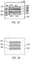
Figure 1A shows a hypothetical reticle 100 corresponding to an IC layout
pattern. For simplicity, the IC pattern consists of three rectangular design features. A
clear reticle glass 110 allows radiation to project onto a resist covered silicon wafer.
Three rectangular chromium regions 102, 104 and 106 on reticle glass 110 block
radiation to generate an image corresponding to intended IC design features.
As light passes through the reticle, it is refracted and scattered by the chromium
edges. This causes the projected image to exhibit some rounding and other optical
distortion. While such effects pose relatively little difficulty in layouts with large
feature sizes (e.g., layouts with critical dimensions above about 1 micron), they can not
be ignored in layouts having features smaller than about 1 micron. The problems
become especially pronounced in IC designs having feature sizes near the wavelength
of light used in the photolithographic process.
Figure 1B illustrates how diffraction and scattering affect an illumination pattern
produced by radiation passing through reticle 100 and onto a section of silicon substrate
120. As shown, the illumination pattern contains an illuminated region 128 and three
dark regions 122, 124, and 126 corresponding to chromium regions 102, 104, and 106
on reticle 100. The illuminated pattern exhibits considerable distortion, with dark
regions 122, 124, and 126 having their corners rounded and their feature widths
reduced. Other distortions commonly encountered in photolithography (and not
illustrated here) include fusion of dense features and shifting of line segment positions.
Unfortunately, any distorted illumination pattern propagates to a developed resist
pattern and ultimately to IC features such as polysilicon gate regions, vias in dielectrics,
etc. As a result, the IC performance is degraded or the IC becomes unusable.
To remedy this problem, a reticle correction technique known as optical
proximity correction (
OPC
) has been developed. Optical proximity correction
involves adding dark regions to and/or subtracting dark regions from a reticle design at
locations chosen to overcome the distorting effects of diffraction and scattering.
Typically, OPC is performed on a digital representation of a desired IC pattern. First,
the digital pattern is evaluated with software to identify regions where optical distortion
will result. Then the optical proximity correction is applied to compensate for the
distortion. The resulting pattern is ultimately transferred to the reticle glass.
Figure 1C illustrates how optical proximity correction may be employed to
modify the reticle design shown in Figure 1A and thereby better provide the desired
illumination pattern. As shown, a corrected
reticle 140 includes three base
rectangular
features 142, 144, and 146 outlined in chromium on a
glass plate 150. Various
corrections
have been added to these base features. Some correction takes the form
of
serifs 148a-148f and 149a-149f. Serifs are small appendage-type addition or
subtraction regions typically made at corner regions on reticle designs. In the example
shown in Figure 1C, the serifs are square chromium extensions protruding beyond the
comers of
base rectangles 142, 144, and 146. These features have the intended effect of
sharpening
the corners of the illumination pattern on the wafer surface. In addition to
serifs, the
reticle 140 includes
segments 151a-151d to compensate for feature thinning
known to result from optical distortion.
Figure 1D shows an illumination pattern 160 produced on a wafer surface 160
by radiation passing through the reticle 140. As shown, the illuminated region includes
a light region 168 surrounding a set of dark regions 162, 164 and 166 which rather
faithfully represent the intended pattern shown in Figure 1A. Note that the illumination
pattern shown in Figure 1B of an uncorrected reticle has been greatly improved by use
of an optical proximity corrected reticle.
Obviously, the degree of optical proximity correction (i.e., the size and location
of correction segments) for any IC feature depends upon the desired IC feature size and
the location of such feature with respect to other IC features. For example, the width of
any one of segments 151a-151d may have to be increased or decreased if the width of
any of the base rectangles 142, 144, and 146 is increased or decreased or if the spacing
between any of these base rectangles is increased or decreased.
Today, the degree of correction necessary for a given feature is determined
largely by empirical methods. That is, experiments are conducted with reticles having
test
patterns to determine the illumination pattern produced on a wafer by light
shown through the test pattern. The deviation between the actual illumination pattern
and the desired feature pattern is used to determine how much optical proximity
correction is required for a reticle used to produce the desired feature pattern. For
example, the
reticle 100 of Figure 1A may be used as a test reticle. A single
experiment would show that the illumination pattern produced by
reticle 100
corresponds to that shown in Figure 1B. The rounding and thinning effects observed
would lead an OPC designer to specify that when the pattern of Figure 1A is desired,
the corrections shown in Figure 1C should be employed. Specifically, the designer
would specify the width and location of
segments 151a-151d and
serifs 148a-148f and
149a-149f.
Of course, these particular corrections apply only to patterns having the exact
size and geometry shown in Figure 1A. If the width of or separation between the base
rectangles changes (in a different IC design for example), the widths and locations of
segments 151a-151d would also have to change. Thus, additional experiments with
test reticles having patterns of differing feature widths and separations would be
necessary to accurately determine the degree of optical proximity correction required for
a changed pattern. Given the huge range of IC feature variations on even a single chip,
a potentially infinite number of test reticles would have to be produced to account for
every pattern that might be encountered. Luckily, for most patterns, it has been found
that the degree of optical proximity correction can be estimated with good accuracy by
interpolating linearly between the actual amount of correction found to be necessary for
two test patterns
straddling
(in terms of sizing and/or spacing) a real feature on an IC
design. Further, the degree of correction for very small patterns lying beyond a range
of experimental patterns may often be predicted with good accuracy by linear
extrapolation. Because these techniques require that only a relatively few test reticles be
generated, many OPC systems in use today employ such linear interpolation and
extrapolation techniques.
Unfortunately, it has been found that as feature sizes decrease beyond a certain
critical dimension (in some cases about 0.5 microns for ultra-violet radiation), the
above-described linear interpolation/extrapolation techniques no longer work well. This
is because the amount of correction required for a given pattern no longer varies in a
linear fashion.
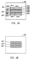
The non-linear effect is depicted in Figures 2A and 2B. Figure 2A shows a
reticle 200 having critical dimensions below a linear threshold (e.g., below about 0.5
microns). When a linear optical proximity correction is performed to correct for optical
distortions expected in the linear regime, the resulting illumination pattern is
unacceptably distorted. Specifically, it has been observed that although serifs 228a-228f
and 229a-229f and segments 251a-251d can be added to the reticle design in a
manner predicted by conventional linear interpolation/extrapolation, inappropriate
fusing and thinning of bars 262, 264, and 266 appear in the illumination pattern on a
substrate 260 as shown in Figure 2B.
To remedy this problem, one might suggest performing more tests in the non-linear
regime and using the test results to develop a more detailed OPC protocol.
However, the number of experiments required would consume too many resources to
be cost effective. Thus, what is needed is an improved method and apparatus for
correcting photolithography reticle design patterns having critical dimensions in the
non-linear regime without requiring a great many additional experiments.
Summary of the Invention
The present invention fills this need by providing an optical proximity
correction method which employs a non-linear mathematical function for determining
the amount of correction required for an arbitrary IC pattern having dimensions in the
non-linear correction regime. The non-linear function should be developed to
accurately depict the variation in required optical proximity correction with decreasing
critical dimension in the non-linear regime described above. In one aspect, the present
invention provides an optical proximity correction method which can be characterized
as including the following steps: (a) performing pattern recognition on an integrated
circuit layout design to identity a location of a selected feature edge in the layout design;
(b) obtaining an optical proximity correction value for the selected feature edge by
evaluating one or more non-linear mathematical expressions for optical proximity
correction at the location of the selected feature edge; and (c) incorporating the optical
proximity correction value into the layout design to form a reticle design.
Preferably, the above steps are repeated many times to scan multiple feature
edges in the layout design. For each such feature edge, the method preferably
determines whether that feature edge is associated with a feature having a critical
dimension above a pre-selected value. If so, the method skips steps (b) and (c) above.
In this manner, unnecessary computation is avoided as larger features reap relatively
little benefit from OPC. Preferably, the pre-selected value is about 0.5 µm or greater: at
least for conventional photolithography performed with ultra-violet radiation.
The non-linear mathematical expression(s) may be evaluated by directly solving
the expression. However, for computation efficiency, it may be desirable to store the
expression as a series of discreet optical proximity correction values generated from the
non-linear mathematical expression. Then when a feature edge is to be evaluated, the
degree of correction is picked off of a look-up table of discreet points rather than
solving a complicated mathematical expression.
In preferred embodiments, the non-linear mathematical expressions are
evaluated at coordinates provided as combinations of at least (i) one value representing
the width of a light transmitting region adjacent to the selected feature edge, and (ii) a
second value representing a width of a light blocking region adjacent to the selected
feature edge. Thus, the degree of correction is a function of both the feature width and
the interfeature spacing adjacent the feature. The resulting correction is sometimes
confirmed against one or more predetermined rules. Such rules may specify the
minimum spacing between adjacent light blocking regions for a particular design
family.
In another aspect, the invention provides an apparatus for performing optical
proximity correction on layout designs to be used in photolithography. The apparatus
may be characterized as including the following components: (a) means for performing
pattern recognition on an integrated circuit layout design to identify locations of selected
feature edges in the layout design; and (b) means for obtaining an optical proximity
correction value for at least one of the selected feature edges by evaluating one or more
non-linear mathematical expressions for optical proximity correction at the location of
the at least one selected feature edge. In further preferred embodiments, the apparatus
includes means for determining whether the selected feature edges are associated with
features having a critical dimension of at most about a predefined value. When such
means for determining finds that a particular feature edge is associated with a feature
having a critical dimension greater than the predefined value, an optical proximity
correction value is not obtained. As noted above, this improves computational
efficiency. It should be noted that the apparatus of this invention will preferably be
implemented as software on a digital computer system. This is particularly convenient,
as most IC designs are today provided in digital form. The software of this invention
simply acts on the IC designs as described to generate a reticle design which can be
printed on an actual reticle.
These and other features and advantages of the present invention will become
apparent upon reading the following detailed descriptions and studying the various
figures of the drawings.
Brief Description of the Drawings
Figure 1A illustrates a conventional reticle having an IC design pattern outlined
in, for example, chromium on a glass backing.
Figure 1B shows an illumination pattern produced on a substrate by light
shown through the reticle of Figure 1A. The illumination pattern exhibits rounding and
thinning effects that result when no optical proximity correction is performed.
Figure 1C illustrates a conventional reticle design employing optical proximity
correction to overcome the rounding and thinning effects in the illumination pattern of
Figure 1B.
Figure 1D shows an improved illumination pattern produced on a substrate by
light shown through the optical proximity corrected reticle of Figure 1C.
Figure 2A illustrates a conventional optical proximity corrected reticle design
for an IC design having critical dimensions in a non-linear correction regime.
Figure 2B shows a resulting fused illumination image produced on a substrate
by light shown through the reticle of Figure 2A.
Figure 3 shows, in accordance with one aspect of the present invention, a
plurality of experimentally determined OPC values plotted as functions feature size and
spacing size (critical dimensions) for patterns in the linear and non-linear regimes.
Figure 4 illustrates, in one embodiment, a mathematical expression designed to
express OPC values as functions feature size and spacing size (critical dimensions) for
patterns in the linear and non-linear regimes.
Figure 5 illustrates, an exemplary reticle test pattern used to generate a empirical
OPC corrections necessary to derive the mathematical function presented in Figure 4.
Figure 6 is a process flow diagram illustrating the steps involved in developing
a corrected reticle design in accordance with one embodiment of this invention.
Figure 7A illustrates a novel reticle design employing optical proximity
correction obtained from a non-linear function to overcome the problematic effects
noted in the illumination pattern of Figure 2B.
Figure 7B shows an improved illumination pattern produced on a substrate by
light shown through the optical proximity corrected reticle of Figure 7A.
Detailed Description of the Preferred Embodiments
Figures 1A-D and 2A-B, as described above, illustrate that some conventional
optical proximity correction methods are unable to correct reticle design patterns having
very small critical dimensions (e.g., below about 0.5 microns). The present invention
utilizes non-linear mathematical expressions to ascertain the degree of correction
required for any such patterns having critical dimensions in such non-linear domain.
The necessary non-linear mathematical expressions may be generated by various
means. In a preferred embodiment, they are generated by curve fitting data from
experiments on incrementally sized reticle designs having critical dimensions in the
non-linear region. They may also be generated from computer simulated data of
patterns having critical dimensions in the non-linear region.
A. PREPARING EXPRESSIONS FOR NON-LINEAR OPTICAL
PROXIMITY CORRECTION
The method for preparing non-linear expressions for OPC in accordance with
the present invention will now be described with reference to Figures 3 through 5.
Referring first to Figure 3, there is shown a graph 300 including mock experimental
optical proximity correction values plotted versus (1) a critical dimensions based upon
feature size (plotted above the horizontal axis), and (2) critical dimensions based upon
spacing between features (plotted below the horizontal axis). By way of example, a
critical dimension based upon feature size might be the width of dark region 122 shown
in Figure 1B, while a critical dimension based upon spacing might be the distance
between dark regions 122 and 124 in Figure 1B. In general, the features described
herein correspond to IC features such as transistor gate electrodes, metallization
conductive lines and the like.
Returning to Figure 3, representative data points taken from hypothetical test
reticles are plotted on a grid having a vertical axis 328 representing optical proximity
correction values and a horizontal axis 326 representing the critical dimension (in
feature size and spacing between features). As can be seen for values of critical
dimension above a point 332, optical proximity correction values vary in a generally
linear manner. However, below point 332, the optical proximity correction values vary
non-linearly. Specifically, points 302, 304, 306, 308, 310, and 312 specify the degree
of correction for feature widths in the non-linear regime, while points 280, 282, and
284 specify the degree of correction for feature widths in the linear regime. Similarly,
points 314, 316, 318, 320, 322, and 324 specify the degree of correction required for
interfeature spacing in the non-linear regime, while points 334, 336, and 338 specify the
degree of correction required for interfeature spacing in the linear regime.
For ultra-violet radiation at about 365 nm, the transition between linear and non-linear
domains (point 332) sometimes corresponds to a critical dimension of
approximately 0.5 microns for both feature width and interfeature spacing. Of course,
the transition between the linear and non-linear regions may occur more gradually than
depicted in Figure 3.
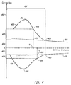
Figure 4 presents a graphical representation 400 of two non-linear mathematical
expressions 406 and 408 which provide optical proximity correction values as a
continuous function of feature width (in the case of expression 406) and interfeature
spacing (in the case of expression 408). As before, a vertical axis 402 specifies the
value of optical proximity correction, while a horizontal axis specifies critical
dimension. In a preferred embodiment, expression 406 is generated by curve fitting
feature width test data and curve 408 is generated by curve fitting interfeature spacing
test data (such as the data illustrated in Figure 3). The resulting mathematical
expressions have an identifiable non-linear region 401 which extends below point 430
for expression 406, and below point 432 for expression 408. Above points 430 and
432, the expressions 406 and 408 vary in a substantially linear fashion.
Preferably, the non-linear expressions generated in accordance with this
invention are devised to apply a relatively wide range expected photolithography
conditions. In this manner, a single expression (or group of expressions) can be used
in photolithography systems where conditions such as depth of focus vary significantly
over the surface of a single wafer. Further, such expression(s) could be used with
various photolithography systems which may employ different light intensities for
example. To generate in non-linear expressions in accordance with this goal, it may be
necessary to conduct multiple experiments with a single reticle under the various
conditions described above. Then an appropriate non-linear mathematical expression
could be tailored to be accurate over rather wide conditions. In some cases, it may be
desirable to include in the expression a term or factor that can be adjusted or calibrated
for a variations in a specific condition such as depth of focus.
Returning to Figure 4, the figure illustrates the difficulty associated with
applying a conventional linear interpolation/extrapolation technique to reticle designs for
features having critical dimensions in the non-linear domain. For example, if a
hypothetical feature edge has an associated width
B,
then the correct optical
proximity correction value for that feature edge would be identified with a
point 416 on
non-linear curve 406. Unfortunately if instead of the non-linear correction employed
with the present invention, a conventional linear extrapolation technique was employed,
a correction value associated with a
point 414 would be obtained. As can be seen,
point
414 is located on a
line 410 extrapolated from known correction values associated with
larger critical dimensions in the linear regime, and the linear correction value associated
with
point 414 is separated from the non-linear correction value associated with
point
416 by an
increment 422.
Similar results occur for interfeature spacing corrections based on non-linear
curve 408. For example, if a hypothetical spacing having a critical dimension "S" is
selected, the degree of optical proximity correction would be associated with a point
420, as shown on curve 408. As above, linear extrapolation techniques would provide
an insufficient degree of correction. Specifically, the degree of correction associated
with linear extrapolation would be a value at a point 418 on a linear extrapolation line
412. As can be seen, point 418 is associated with the linear correction factor 426
(presented on vertical axis 402), which is short of the actual correction value by an
additional non-linear correction factor 428.
Thus, it has been recognized that the amount of optical proximity correction
varies non-linearly for critical dimensions below a threshold region (e.g., about 0.5
microns). The present invention builds on this recognition by generating non-linear
mathematical expressions which accurately represent optical proximity correction
values for reticle designs having feature widths and/or feature spacings in the non-linear
regime.
It should be noted that in many instances, it has been observed that curves 406
and 408 change direction at points 434 and 436, respectively. While the present
invention can in theory be applied to features having critical dimensions smaller than
points 434 and 436, such features are typically too small to be imaged with radiation at
conventional wavelengths (e.g., the visible or ultra-violet regions of the electromagnetic
spectrum). As a result, shorter wavelength radiation (e.g., X-rays) must be used to
image smaller feature patterns.
In general, the non-linear mathematical expressions of this invention may be
analytic expressions (e.g., polynomials) or numerical expressions. An analytic
expression of this invention may take on a form such as VOPC = f(x,y,z), where
VOPC is the value of the optical proximity correction and f(x,y,z) is an analytic or
numerical expression of the variables x, y, and z. In a some embodiments, only a
single variable is used in the expression. That variable might be the value of the feature
width or the interfeature spacing at a location of interest. In some embodiments, two or
even three variables may be employed in the same expression. These may be the
feature width, the interfeature spacing, the angle of a feature, or any of a number of
other parameters associated with the feature edge of interest.
In one embodiment, the non-linear mathematical expression is stored as a
comprehensive lookup table constructed by evaluating the expression at numerous
critical dimension values. Using such lookup tables generally simplifies software
operations and speeds up computation.
Figure 5 shows a simple standardized reticle test pattern 500 known as a
paddle structure
which may be used to generate data for use in preparing a non-linear
expression in accordance with this invention. In practice, a resist coated wafer is
exposed to light passing through reticle 500. The resist is subsequently developed and
the resulting pattern is evaluated with scanning electron microscopy to determine the
degree of necessary correction.
The paddle structure has been found to efficiently provide various types of data.
Specifically, the structure includes both a dense collection of features in its lower
portion ( bars 502, 504, 506, 508, and 509) and an isolated feature in its upper portion
(bar 506). In general, the amount of correction required is a function of the local feature
density, with isolated features requiring a certain amount and type of correction and
dense features sometimes requiring a different amount and type of correction. Thus, by
performing a single experiment on a reticle with a paddle pattern of a given size and
shape, at least two valuable pieces of information can be obtained.
B. METHOD OF PERFORMING OPTICAL PROXIMITY CORRECTION IN
THE NON-LINEAR DOMAIN
Figure 6 illustrates a process of the present invention for performing optical
proximity correction in the non-linear regime. The process begins at 700 and in a step
702 determines which integrated circuit design level will be subjected to optical
proximity correction. It should be understood that integrated circuits are formed with
many different mask levels, each of which requires its own reticle. For example, one
level may define the pattern for a p-type well implant, another level may define a
transistor gate electrode pattern, yet another level may define a first metallization
interconnection pattern, etc. For purposes of the process at hand, a design layout for a
single level is selected for correction at step 702.
Next, the initial layout design for the selected layout level is obtained and a scan
of its features is started at a
step 704. The scanning process begins at an arbitrarily
selected position of the layout design and proceeds in a defined direction until a feature
edge is located. Such edge represents the boundary of a protected and unprotected
region on a mask. After the current edge is identified at
step 704, the method proceeds
to a
step 706 where coordinates associated with the current edge are generated. In a
preferred embodiment, these coordinates include (1) the width of the feature (e.g., the
protected region) at the current edge, and (2) the width of the space (e.g., the
unprotected region) between the current edge and the edge of the next adjacent feature.
The second coordinate has been referred to above as the
interfeature spacing.
Other
possible coordinates associated with the current edge include the edge position of the
next successive bar and/or space (beyond the bar and space associated with the current
edge itself), the angle of the current edge, etc. In some embodiments, the method
includes an additional step of determining whether a feature size exceeds a critical
dimension (e.g., one micron). If so, current edge is ignored and the next edge is
located. This may substantially improve the computational efficiency of the method by
eliminating unnecessary correction calculations.
After the current edge coordinates have been identified in step 706, the method
proceeds to a step 708 where the coordinates are evaluated with a non-linear
mathematical expression obtained as described above in connection with Figure 4. As
shown in Figure 4, a particular value of optical proximity correction may be obtained
for a feature width or an interfeature spacing or both. If both the feature width and the
interfeature spacing are used to determine the correction, the non-linear correction
expression should be written as a function of at least those two variables. In such
cases, the two curves 406 and 408 shown in Figure 4 would have to be merged in a
single function that could be depicted in three-dimensional space.
After the degree of optical proximity correction has been determined for the
current edge at step 708, a step 710 performs a correction on the current edge. For
example, the feature width may be increased or reduced at that edge, a serif may be
added at the edge (see Figure 1C for example), etc. In addition, correction may also
entail shifting entire features in an attempt to prevent features from fusing together.
From step 710, the method proceeds to a step 712 where a decision is made as to
whether anymore edges are present in the current IC design layout level. If there are
more edges, then process control reverts to step 702 where the next edge is identified
by scanning in the original direction until the next edge is located. At that point, the
new edge becomes the current edge and process steps 706, 708, and 710 are performed
at the new current edge. Then, it is determined at step 712 whether any more edges are
present.
When all edges in the design layout have been processed and corrected as
necessary, (i.e., there are no more edges present in the layout design of the current
level), the method proceeds to a step 714 where it is determined whether there are any
more design levels. If there are more design levels, the method proceeds to a step 716
where the next design level is obtained. For example, if a layout for a via level has just
been completely corrected, step 716 may obtain the design layout for a first
metallization layer to be formed immediately on top of the via level. From step 716,
the method proceeds to step 702, and from there through steps 704, 706, 708, 710,
712, and if no more edges are present for that level, then the method proceeds to step
714. When all design layout levels to be corrected have been corrected (i.e., decision
step 714 is answered in the negative), then the optical proximity correction method is
completed at 718.
It should be recognized that the above method is typically implemented as
software on a digital computer system. The IC layout designs are provided as digitized
patterns defining a desired mask layout on a chip. These digitized patterns are scanned
with pattern recognition software which can identify edges and associated
feature/spacing sizes. The pattern recognition software may even identify and choose to
ignore features that are greater than a predefined size, e.g., one micron. Ultimately, the
completely corrected reticle design is formed on an actual reticle such as a glass and
chrome reticle.
The non-linear optical proximity correction function may be provided in the
form of a programmed equation that can be directly evaluated for each set of
coordinates that it receives. More preferably, however, the non-linear function is
initially evaluated at numerous dimensions and stored in the form of a look-up table
containing a series of discreet points corresponding to correction values for the
corresponding feature dimensions. When a new coordinate is provided by the pattern
recognition software, the nearest point from the look-up table is identified and used to
provide the necessary correction value. Storing the non-linear mathematical function in
the form of a look-up table significantly improves computational efficiency.
To further illustrate how the above described method may be implemented,
reference is again made to Figure 5. Specifically, the paddle pattern of Figure 5 will
now be assumed to be an IC design pattern that is to be subjected to non-linear optical
proximity correction. As explained above, paddle structure 500 has four identically
sized features (bars) 502, 504, 508 and 509 straddling a longer feature 506 having an
isolated section at the top of the paddle pattern. In this technique, the optical proximity
correction software scans the paddle in a raster-like manner in order to identify all
feature edges. During the scanning process, various edges are identified on paddle
structure 500.
In one embodiment, the scanning process begins in the lower left corner of the
pattern and proceeds horizontally across the pattern. The first feature edge encountered
will be 530a. In the context of the Figure 6 flow diagram, edge 530a becomes the
current edge (step 704). Thereafter, appropriate coordinates are obtained, the degree of
correction is ascertained, and the correction is made as described with respect to steps
706, 708, and 710. Next, the pattern is horizontally scanned until the next feature edge
536a is identified. This edge is then evaluated per steps 706, 708, and 710. Continuing
in this vein, edges 536b, 536c,...536n are encountered, evaluated, and corrected as
specified by the non-linear functions described above.
When the end of the right edge of the pattern is encountered, the scanning
process increments to a vertically adjacent position and again begins horizontal
scanning. For example, the process may next encounter edge 530b. After evaluating
and correcting that edge, the next successive edges are located and corrected as
described until the right edge of the pattern is again encountered. At that point, the edge
530c is located and corrected. The scanning and correcting process continues in this
manner through edge 528n where the pattern changes. At the next vertical increment,
only a single feature will be found. Thus, after the top of bars 502, 504, 508, and 509
have been surpassed, the next edge encountered will be 522a. This edge is, of course,
corrected as described above. The process thereafter continues through edges 522b,
520a, and 520b.
Often the scanning process will then be repeated in a vertical rasterized manner
to pick off and correct horizontally aligned edges. In some IC layout designs, it may
also he necessary to conduct raster scans in the diagonal directions at 45° (or some
other angle) with respect to the vertical. The diagonal scans may be employed in
designs having lines and other features oriented diagonally with respect to the main grid
of the chip.
Each time an edge is encountered, relevant coordinates associated with that edge
must be generated (step 706 of Figure 6). For example, when feature edge 536a is
encountered during the scan, the feature width (e.g., the width of bar 502) forms one
coordinate, and the interfeature spacing 510a between bar 502 and next adjacent bar 504
forms a second coordinate. Similar coordinates for edge 536b include the width of bar
504 and the spacing 510a For edge 536c, the coordinates include the width of bar 504
and spacing 510b. Spacings 510c and 510d would be used in the coordinates of other
edges. Edges with no close adjacent features (e.g., edges 520a, 522b, 530a, and 536n)
will have a coordinate selected to indicate this condition (e.g. infinity). In a preferred
embodiment, any feature separated from an adjacent feature by one micron or more
will meet this condition. Certain rules may apply to correcting features with such
edges.
For simplicity and efficiency, the scanning process preferably is programmed to
ignore critical dimensions greater than about one micron. This is done to increase
correction speed for critical dimensions in the non-linear regime. As mentioned above,
slight distortions impact sub-micron IC features more severely than IC features having
critical dimensions larger than about one micron. In addition, the greater the number of
corrections performed, the greater the number of possible errors produced. For
example,
slivers
may be inadvertently introduced in an attempt to correct a particular
feature geometry. Silvers are common in optical proximity correction, and they many
consist of small serifs or segments that are intended to append to an IC feature, but are
inadvertently left floating (i.e., unattached to a feature). Thus, limiting optical proximity
correction to sub-micron features increases efficiency and avoids introducing additional
opportunities for errors.
It should be noted that in addition to the basic calculation of optical proximity
correction required for each feature edge, the method of the present invention may
employ various design rules to supplement the correction values. Some of these rules
may negate a correction provided by the non-linear expressions of this invention. Other
rules may modify the correction value without negating the correction. Such rules are
typically applied when a given feature and its local environment meet certain criteria
Such rules may, for example, specify a minimum interfeature spacing for a particular
design family. More specifically, such minimum interfeature may be selected to be
between about 0.2 and 0.5 microns (which might be varied within this range by 0.01
microns).
Figure 7A represents a reticle pattern having feature edges with critical
dimensions in the non-linear regime (e.g., critical dimensions below about 0.5
microns). As illustrated in Figure 2B, conventional optical proximity correction of an
amount calculated for a linear case fails to prevent fusing in the developed resist
regions. However, the non-linear optical proximity correction method of this invention
is able to provide a correct degree of correction for very small features.
As shown in Figure 7A, a reticle 600 includes three symmetric features 602,
604, and 606. In addition, after the appropriate corrections have been determined from
the appropriate non-linear function, specific corrective segments and/or serifs were
added. Specifically, the particular corrective serifs include regions 628a through 628f
and 629a through 629f appended to each of the corners of features 602, 604 and 606.
In addition, segments 651a through 651d were added to prevent feature thinning.
Although no serifs or segments were shown subtracted from features 602, 604 and
606, more complex IC designs may require such corrective deletions.
Figure 7B shows an illumination pattern produced on a substrate 660 by light
shining through reticle 600. As can be seen, illumination pattern 660 includes three
dark regions 662, 664, and 666 separated from one another. For example, dark regions
662 and 664 are separated from one another by a light region 668. In contrast, the
illumination pattern created by a linearly corrected reticle (e.g., see Figure 2B) has fused
dark regions. As mentioned above, the fused resist structure of Figure 2B is a product
of applying conventional optical proximity correction which fails to consider the non-linear
behavior of correction associated with critical dimensions below a transition
dimension (e.g., about 0.5 microns).
Although the preferred embodiments of the present invention have been
described in detail, it should be understood that the present invention may be embodied
in many other specific forms without departing from the spirit or scope of the
invention. Therefore, the present examples and embodiments are to be considered as
illustrative and not restrictive, and the invention is not to be limited to the details given
herein, but may be modified within the scope of the appended claims.