EP0817540A2 - Electroluminescent structure using lamellar electrodes - Google Patents
Electroluminescent structure using lamellar electrodes Download PDFInfo
- Publication number
- EP0817540A2 EP0817540A2 EP97110256A EP97110256A EP0817540A2 EP 0817540 A2 EP0817540 A2 EP 0817540A2 EP 97110256 A EP97110256 A EP 97110256A EP 97110256 A EP97110256 A EP 97110256A EP 0817540 A2 EP0817540 A2 EP 0817540A2
- Authority
- EP
- European Patent Office
- Prior art keywords
- layer
- electroluminescent
- lamellar
- electroluminescent element
- anode
- Prior art date
- Legal status (The legal status is an assumption and is not a legal conclusion. Google has not performed a legal analysis and makes no representation as to the accuracy of the status listed.)
- Withdrawn
Links
Classifications
-
- H—ELECTRICITY
- H05—ELECTRIC TECHNIQUES NOT OTHERWISE PROVIDED FOR
- H05B—ELECTRIC HEATING; ELECTRIC LIGHT SOURCES NOT OTHERWISE PROVIDED FOR; CIRCUIT ARRANGEMENTS FOR ELECTRIC LIGHT SOURCES, IN GENERAL
- H05B33/00—Electroluminescent light sources
- H05B33/12—Light sources with substantially two-dimensional radiating surfaces
- H05B33/26—Light sources with substantially two-dimensional radiating surfaces characterised by the composition or arrangement of the conductive material used as an electrode
-
- H—ELECTRICITY
- H10—SEMICONDUCTOR DEVICES; ELECTRIC SOLID-STATE DEVICES NOT OTHERWISE PROVIDED FOR
- H10K—ORGANIC ELECTRIC SOLID-STATE DEVICES
- H10K50/00—Organic light-emitting devices
- H10K50/80—Constructional details
- H10K50/805—Electrodes
- H10K50/81—Anodes
- H10K50/816—Multilayers, e.g. transparent multilayers
-
- H—ELECTRICITY
- H10—SEMICONDUCTOR DEVICES; ELECTRIC SOLID-STATE DEVICES NOT OTHERWISE PROVIDED FOR
- H10K—ORGANIC ELECTRIC SOLID-STATE DEVICES
- H10K85/00—Organic materials used in the body or electrodes of devices covered by this subclass
- H10K85/10—Organic polymers or oligomers
- H10K85/111—Organic polymers or oligomers comprising aromatic, heteroaromatic, or aryl chains, e.g. polyaniline, polyphenylene or polyphenylene vinylene
- H10K85/113—Heteroaromatic compounds comprising sulfur or selene, e.g. polythiophene
- H10K85/1135—Polyethylene dioxythiophene [PEDOT]; Derivatives thereof
-
- H—ELECTRICITY
- H10—SEMICONDUCTOR DEVICES; ELECTRIC SOLID-STATE DEVICES NOT OTHERWISE PROVIDED FOR
- H10K—ORGANIC ELECTRIC SOLID-STATE DEVICES
- H10K85/00—Organic materials used in the body or electrodes of devices covered by this subclass
- H10K85/60—Organic compounds having low molecular weight
- H10K85/631—Amine compounds having at least two aryl rest on at least one amine-nitrogen atom, e.g. triphenylamine
- H10K85/633—Amine compounds having at least two aryl rest on at least one amine-nitrogen atom, e.g. triphenylamine comprising polycyclic condensed aromatic hydrocarbons as substituents on the nitrogen atom
-
- H—ELECTRICITY
- H10—SEMICONDUCTOR DEVICES; ELECTRIC SOLID-STATE DEVICES NOT OTHERWISE PROVIDED FOR
- H10K—ORGANIC ELECTRIC SOLID-STATE DEVICES
- H10K85/00—Organic materials used in the body or electrodes of devices covered by this subclass
- H10K85/60—Organic compounds having low molecular weight
- H10K85/649—Aromatic compounds comprising a hetero atom
- H10K85/657—Polycyclic condensed heteroaromatic hydrocarbons
- H10K85/6572—Polycyclic condensed heteroaromatic hydrocarbons comprising only nitrogen in the heteroaromatic polycondensed ring system, e.g. phenanthroline or carbazole
-
- H—ELECTRICITY
- H10—SEMICONDUCTOR DEVICES; ELECTRIC SOLID-STATE DEVICES NOT OTHERWISE PROVIDED FOR
- H10K—ORGANIC ELECTRIC SOLID-STATE DEVICES
- H10K50/00—Organic light-emitting devices
- H10K50/10—OLEDs or polymer light-emitting diodes [PLED]
- H10K50/17—Carrier injection layers
Definitions
- An electroluminescent (EL) arrangement is characterized in that it emits light under the application of an electrical voltage under current flow.
- polymers such as poly- (p-phenylene) and poly- (p-phenylene vinylene (PPV)) as electroluminescent polymers: G. Leising et al., Adv. Mater. 4 (1992) No. 1; Friend et al., J. Chem. Soc., Chem. Commun. 32 (1992); Saito et al., Polymer, 1990, Vol. 31, 1137; Friend et al., Physical Review B, Vol. 42, No. 18, 11670 or WO 90/13148. More examples of PPV in electroluminescent displays are described in EP-A 443 861, WO-A-9203490 and 92003491 described.
- EP-A 0 294 061 presents an optical modulator based on polyacetylene.
- an EL arrangement consists of two electrodes, between which there is an organic layer that functions - including the emission of light - fulfilled.
- Such systems are e.g. in the Application WO 90/13148 based on poly (p-phenylene vinylene) is described.
- the construction of multilayer systems can be carried out by vapor deposition processes the layers are applied successively from the gas phase or by casting processes respectively. Casting processes are due to the higher process speeds prefers. However, the dissolving process represents one that has already been brought up Layer is difficult when layering with the next layer.
- the object of the present invention is to provide lamellar Base electrodes, which are the cost-effective production of electroluminescent, allow organic layer systems (O-LEDs).
- O-LEDs are described, the base electrode of which consists of transparent, electrically conductive oxides, such as indium tin oxide (ITO), or of semi-transparent metal layers, such as gold.
- ITO indium tin oxide
- gold semi-transparent metal layers
- ITO is used for all the examples listed. ITO has the advantage over the other materials that it has a relatively large electron work function (see, for example, ID Parker, J. Appl. Phys. 75 , (1994), 1656-1666).
- ITO substrates high quality and low surface roughness can be used.
- the present invention describes a lamellar base electrode with which the above difficulties can be solved as well as the electroluminescent Arrangement itself.
- the base electrode according to the invention consists of an inorganic layer which is applied directly to the carrier and a second layer, which consists of a Solution out with techniques such as Spin coating, casting, knife coating, cap coating etc., is deposited on the first layer.
- the first, inorganic layer consists of an electrically conductive material, that is transparent or semi-transparent.
- transparent materials such as e.g. Indium tin oxide (ITO), tin oxide, doped zinc oxide and other conductive Metal oxides, or semi-transparent metal layers, e.g. Au, Ag, Cu, Al, Cr, Ni or alloys thereof can be used.
- ITO Indium tin oxide
- tin oxide tin oxide
- doped zinc oxide and other conductive Metal oxides e.g. Au, Ag, Cu, Al, Cr, Ni or alloys thereof can be used.
- semi-transparent metal layers e.g. Au, Ag, Cu, Al, Cr, Ni or alloys thereof can be used. These materials don't have to necessarily large electron work functions, e.g. ITO own. This is required for prior art O-LEDs as mentioned above.
- a material that can be deposited from the solution is applied as the second layer.
- transparent or semi-transparent materials such as Polymers or polymer blends in question.
- Electrically conductive polymers such as Polythiophenes, polypyrroles, polyaniline or polyacetylene are used.
- polythiophenes e.g. polyethylene dioxythiophene / polystyrene sulfonic acid Na salt
- the materials of the second layer must possess great electron work functions to get a good hole injection into the to enable organic, electroluminescent layer system.
- materials with electron work functions greater than 4 eV are preferred greater than 4.3 eV and particularly preferably greater than 4.5 eV used.
- the material of the second layer must have a specific resistance which is less than 10 11 ⁇ cm, preferably less than 10 10 ⁇ cm and particularly preferably less than 10 9 ⁇ cm.
- Deposition of the second layer from a solution results in one very smooth, homogeneous surface of the lamellar base electrode according to the invention, so that short circuits within the O-LED are avoided.
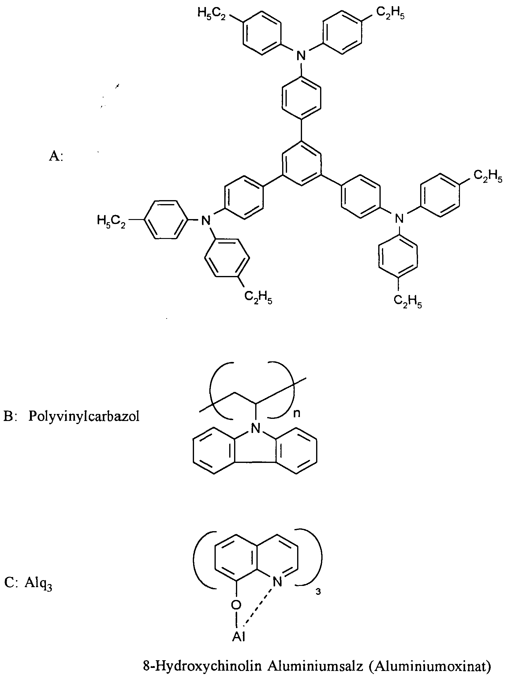
- Electroluminescent arrangement based on a blend system
- a 1% solution consisting of 1 part by weight A, 4 parts by weight B and 1 Part C by weight in dichloroethane is mixed with a commercial spin coater a speed of 400 / min on one with a lamellar electrode coated glass plate.
- the lamellar electrode consists of an approx. 100 nm thick ITO layer on which a 74 nm thick layer of polyethylene dioxythiophene / polystyrene sulfonic acid Na salt (Baytron P, Bayer AG, Leverkusen, Germany) was.
- the coating is carried out according to the information in EP-A 686 662. However the heat treatment described there was dispensed with and the substrate Annealed at 80 ° C under nitrogen for 1 h.
- the layer thickness of the blend system is 100 nm.
- the counter electrode is Mg / Ag in a ratio of 10: 1 through thermal code position upset.
- the arrangement After contacting and application of an electric field, the arrangement shows visually recognizable electroluminescence in the green spectral range from about 8 V.
- the brightness is 89 cd / m 2 at a current of 19.1 mA / cm 2 and a voltage of 17 V.
- the electronic levels of the arrangement are determined as follows. Work function comment ITO 4.7 eV [ID Parker] PEDT / PSS Baytron P 5.1 eV own measurement (Kelvin probe)
- Electroluminescent arrangement based on a blend system
- the lamellar electrode consists of a tin oxide layer on a 4 mm Flat glass on which a 74 nm thick layer of polyethylenedioxythiophene / polystyrene sulfonic acid Na salt had been hurled.
- the coating takes place according to the information in EP-A 686 662. However, attention has been paid to the one described there No heat treatment and the substrate at 80 ° C under nitrogen for 1 h annealed.
- the layer thickness of the hole-conducting layer is approximately 70 nm.
- An electron-conducting or emitting layer consisting of Alq 3 is evaporated onto this hole-conducting layer at 10 -6 mbar.
- the layer thickness is approx. 60 nm.
- a MgAg alloy in a ratio of 10: 1 is applied as the counter electrode by thermal code position.
- the system emits the green light.
- the brightness is 550 Cd / m 2 at a current of 14 mA / cm 2 and a voltage of 12 volts.
- ionization potentials or the highest occupied molecular bitals (HOMO) of typical organic hole conductors are in the range from 5.1 to 5.5 eV (see C. Adachi, K. Nagai, N. Tamoto, Appl. Phys. Lett. 66 ( 1995) 2679-2681).
Abstract
Description
Eine elektrolumineszierende (EL) Anordnung ist dadurch charakterisiert, daß sie unter Anlegung einer elektrischen Spannung unter Stromfluß Licht aussendet. Derartige Anordnungen sind unter der Bezeichnung "Leuchtdioden" (LEDs = light emitting diodes) seit langem in der Technik bekannt. Die Emission von Licht kommt dadurch zustande, daß positive Ladungen ("Löcher", holes) und negative Ladungen ("Elektronen", electrons) unter Aussendung von Licht rekombinieren.An electroluminescent (EL) arrangement is characterized in that it emits light under the application of an electrical voltage under current flow. Such Arrangements are called "light emitting diodes" (LEDs = light emitting diodes) has long been known in the art. The emission of light comes about because positive charges ("holes", holes) and negative Recombine charges ("electrons") while emitting light.
Bei der Entwicklung lichtemittierender Bauteile für Elektronik oder Photonik kommen heute hauptsächlich anorganische Halbleiter, wie Galliumarsenid, zum Einsatz. Auf Basis derartiger Substanzen können punktförmige Anzeigeelemente hergestellt werden. Großflächige Anordnungen sind nicht möglich.When developing light-emitting components for electronics or photonics come Today mainly inorganic semiconductors such as gallium arsenide are used. Point-like display elements can be produced on the basis of such substances will. Large-scale arrangements are not possible.
Neben den Halbleiterleuchtdioden sind elektrolumineszierende Anordnungen auf Basis aufgedampfter niedermolekularer organischer Verbindungen bekannt (US-P 4 539 507, US-P 4 769 262, US-P 5 077 142, EP-A 406 762).In addition to the semiconductor light-emitting diodes, there are electroluminescent arrangements Based on evaporated low molecular weight organic compounds known (US-P 4,539,507, U.S. Patent 4,769,262, U.S. Patent 5,077,142, EP-A 406,762).
Weiterhin werden Polymere, wie Poly-(p-phenylene) und Poly-(p-phenylenvinylene (PPV)) als elektrolumineszierende Polymere beschrieben: G. Leising et al., Adv. Mater. 4 (1992) No. 1; Friend et al., J. Chem. Soc., Chem. Commun. 32 (1992); Saito et al., Polymer, 1990, Vol. 31, 1137; Friend et al., Physical Review B, Vol. 42, No. 18, 11670 oder WO 90/13148. Weitere Beispiele für PPV in Elektrolumineszenzanzeigen werden in EP-A 443 861, WO-A-9203490 und 92003491 beschrieben.Furthermore, polymers such as poly- (p-phenylene) and poly- (p-phenylene vinylene (PPV)) as electroluminescent polymers: G. Leising et al., Adv. Mater. 4 (1992) No. 1; Friend et al., J. Chem. Soc., Chem. Commun. 32 (1992); Saito et al., Polymer, 1990, Vol. 31, 1137; Friend et al., Physical Review B, Vol. 42, No. 18, 11670 or WO 90/13148. More examples of PPV in electroluminescent displays are described in EP-A 443 861, WO-A-9203490 and 92003491 described.
EP-A 0 294 061 stellt einen optischen Modulator auf Basis von Polyacetylen vor.EP-A 0 294 061 presents an optical modulator based on polyacetylene.
Zur Herstellung flexibler Polymer-LEDs haben Heeger at al. lösliche konjugierte PPV-Derivate vorgeschlagen (WO 92/16023).For the production of flexible polymer LEDs, Heeger at al. soluble conjugated PPV derivatives proposed (WO 92/16023).
Polymerblends unterschiedlicher Zusammensetzung sind ebenfalls bekannt: M. Stolka et al., Pure & Appt. Chem., Vol. 67, No. 1, pp 175-182, 1995; H. Bässler et al., Adv. Mater. 1995, 7, No. 6, 551; K. Nagai et al., Appl. Phys. Lett. 67 (16), 1995, 2281; EP-A 532 798. Polymer blends of different compositions are also known: M. Stolka et al., Pure & Appt. Chem., Vol. 67, No. 1, pp 175-182, 1995; H. Bässler et al., Adv. Mater. 1995, 7, No. 6, 551; K. Nagai et al., Appl. Phys. Lett. 67 (16), 1995, 2281; EP-A 532 798.
Die organischen EL-Anordnungen enthalten in der Regel eine oder mehrere
Schichten aus organischen Ladungstransportverbindungen. Der prinzipielle Aufbau
in der Reihenfolge der Schichten ist wie folgt:
Dieser Aufbau stellt den allgemeinsten Fall dar und kann vereinfacht werden, indem einzelne Schichten weggelassen werden, so daß eine Schicht mehrere Aufgaben übernimmt. Im einfachsten Fall besteht eine EL-Anordung aus zwei Elektroden, zwischen denen sich eine organische Schicht befindet, die alle Funktionen - inklusive der der Emission von Licht - erfüllt. Derartige Systeme sind z.B. in der Anmeldung WO 90/13148 auf der Basis von Poly-(p-phenylenvinylen) beschrieben.This structure represents the most general case and can be simplified, by leaving out individual layers so that one layer has multiple tasks takes over. In the simplest case, an EL arrangement consists of two electrodes, between which there is an organic layer that functions - including the emission of light - fulfilled. Such systems are e.g. in the Application WO 90/13148 based on poly (p-phenylene vinylene) is described.
Der Aufbau von Mehrschichtsystemen kann durch Aufdampfverfahren, bei denen die Schichten sukzessive aus der Gasphase aufgebracht werden oder durch Gießverfahren erfolgen. Gießverfahren sind aufgrund der höheren Prozeßgeschwindigkeiten bevorzugt. Allerdings stellt der Anlöseprozeß einer bereits aufgebrachten Schicht beim Überschichten mit der nächsten Schicht eine Schwierigkeit dar.The construction of multilayer systems can be carried out by vapor deposition processes the layers are applied successively from the gas phase or by casting processes respectively. Casting processes are due to the higher process speeds prefers. However, the dissolving process represents one that has already been brought up Layer is difficult when layering with the next layer.
Die Aufgabe der vorliegenden Erfindung ist die Bereitstellung von lamellaren Basiselektroden, die die kostengünstige Herstellung von elektrolumineszierenden, organischen Schichtsystemen (O-LEDs) erlauben.The object of the present invention is to provide lamellar Base electrodes, which are the cost-effective production of electroluminescent, allow organic layer systems (O-LEDs).
In den oben genannten Veröffentlichungen werden O-LEDs beschrieben, deren Basiselektrode aus transparenten, elektrisch leitfähigen Oxiden, wie z.B. Indium-Zinnoxid (ITO), oder aus semitransparenten Metallschichten, wie z.B. Gold, besteht. In der Regel wird für alle angeführten Beispiele ITO eingesetzt. ITO hat gegenüber den anderen Materialien den Vorteil, daß es eine relativ große Elektronenaustrittsarbeit besitzt (siehe z.B. I.D. Parker, J. Appl. Phys. 75, (1994), 1656-1666).In the publications mentioned above, O-LEDs are described, the base electrode of which consists of transparent, electrically conductive oxides, such as indium tin oxide (ITO), or of semi-transparent metal layers, such as gold. As a rule, ITO is used for all the examples listed. ITO has the advantage over the other materials that it has a relatively large electron work function (see, for example, ID Parker, J. Appl. Phys. 75 , (1994), 1656-1666).
Da die Basiselektrode in der Regel als Anode geschaltet wird, müssen von der Anode her Löcher, d.h. positive Ladungsträger, in die angrenzende, organische Schicht injiziert werden. Dies gelingt umso besser, je größer die Elektronenaustrittsarbeit bzw. das Ionisationspotential ist (vgl. I.D. Parker, J. Appl. Phys. 75 (1994), 1656-1666).Since the base electrode is generally switched as an anode, holes, ie positive charge carriers, must be injected into the adjacent organic layer from the anode. The greater the electron work function or the ionization potential, the better this is achieved (cf. ID Parker, J. Appl. Phys. 75 (1994), 1656-1666).
Setzt man ITO als Basiselektrode ein, so treten folgende Nachteile auf:
(Zinnoxid ist ein vergleichsweise kostengünstigeres Material, das ebenfalls transparent und elektrisch leitfähig ist. Zinnoxid hat jedoch eine niedrigere Elektronenaustrittsarbeit und wird deshalb in der Regel nicht eingesetzt.)
(Tin oxide is a comparatively less expensive material that is also transparent and electrically conductive. However, tin oxide has a lower electron work function and is therefore usually not used.)
Durch die rauhen Oberflächen von ITO treten bei O-LEDs häufig Kurzschlüsse auf, die in einer Fertigung einen hohen Ausschuß bedeuten. Daher müssen ITO-Substrate hoher Qualität und geringer Oberflächenrauhigkeit verwendet werden.Due to the rough surfaces of ITO, short circuits often occur with O-LEDs that mean a high scrap in a production. Therefore ITO substrates high quality and low surface roughness can be used.
Die relativ hohen Kosten von ITO-beschichteten Substraten limitieren das Kostensenkungspotential von O-LEDs.The relatively high costs of ITO-coated substrates limit this Cost reduction potential of O-LEDs.
Die vorliegende Erfindung beschreibt eine lamellare Basiselektrode, mit der die oben genannten Schwierigkeiten gelöst werden können sowie die elektrolumineszierende Anordnung selbst.The present invention describes a lamellar base electrode with which the above difficulties can be solved as well as the electroluminescent Arrangement itself.
Die erfindungsgemäße Basiselektrode besteht aus einer anorganischen Schicht, die direkt auf dem Träger aufgebracht ist und einer zweiten Schicht, die aus einer Lösung heraus mit Techniken wie z.B. Spin-Coating, Gießen, Rakeln, Cap-Coating etc., auf der ersten Schicht abgeschieden wird. The base electrode according to the invention consists of an inorganic layer which is applied directly to the carrier and a second layer, which consists of a Solution out with techniques such as Spin coating, casting, knife coating, cap coating etc., is deposited on the first layer.
Die erste, anorganische Schicht besteht aus einem elektrisch leitfähigen Material, das transparent oder semitransparent ist. Hier können transparente Materialien, wie z.B. Indium-Zinnoxid (ITO), Zinnoxid, dotiertes Zinkoxid und weitere leitfähige Metalloxide, oder semitransparente Metallschichten, wie z.B. Au, Ag, Cu, Al, Cr, Ni oder Legierungen davon, eingesetzt werden. Diese Materialien müssen nicht notwendigerweise große Elektronenaustrittsarbeiten, wie z.B. ITO, besitzen. Dies ist für O-LEDs gemäß dem Stand der Technik, wie oben erwähnt, erforderlich.The first, inorganic layer consists of an electrically conductive material, that is transparent or semi-transparent. Here transparent materials, such as e.g. Indium tin oxide (ITO), tin oxide, doped zinc oxide and other conductive Metal oxides, or semi-transparent metal layers, e.g. Au, Ag, Cu, Al, Cr, Ni or alloys thereof can be used. These materials don't have to necessarily large electron work functions, e.g. ITO own. This is required for prior art O-LEDs as mentioned above.
Als zweite Schicht wird ein aus der Lösung deponierbares Material aufgetragen. Hier kommen transparente oder semitransparente Materialien wie z.B. Polymere oder Polymerblends in Frage. Bevorzugt werden elektrisch leitfähige Polymere wie Polythiophene, Polypyrrole, Polyanilin oder Polyacetylen verwendet. Besonders bevorzugt werden hier Polythiophene (z.B. Polyethylendioxythiophen/Polystyrolsulfonsäure-Na-Salz) eingesetzt. Die Materialien der zweiten Schicht müssen große Elektronenaustrittsarbeiten besitzen, um eine gute Löcherinjektion in das organische, elektrolumineszierende Schichtsystem zu ermöglichen. Vorzugsweise werden Materialien mit Elektronenaustrittsarbeiten größer als 4 eV, bevorzugt größer als 4,3 eV und besonders bevorzugt größer als 4,5 eV eingesetzt.A material that can be deposited from the solution is applied as the second layer. Here come transparent or semi-transparent materials such as Polymers or polymer blends in question. Electrically conductive polymers such as Polythiophenes, polypyrroles, polyaniline or polyacetylene are used. Especially polythiophenes (e.g. polyethylene dioxythiophene / polystyrene sulfonic acid Na salt) are preferred here used. The materials of the second layer must possess great electron work functions to get a good hole injection into the to enable organic, electroluminescent layer system. Preferably materials with electron work functions greater than 4 eV are preferred greater than 4.3 eV and particularly preferably greater than 4.5 eV used.
Um Inhomogenitäten des elektrischen Feldes innerhalb der lamellaren Basiselektrode zu vermeiden, muß das Material der zweiten Schicht einen spezifischen Widerstand aufweisen, der kleiner als 1011 Ω cm, bevorzugt Kleiner als 1010 Ω cm und besonders bevorzugt kleiner als 109 Ω cm ist.In order to avoid inhomogeneities of the electric field within the lamellar base electrode, the material of the second layer must have a specific resistance which is less than 10 11 Ω cm, preferably less than 10 10 Ω cm and particularly preferably less than 10 9 Ω cm.
Durch die Deposition der zweiten Schicht aus einer Lösung heraus ergibt sich eine sehr glatte, homogene Oberfläche der erfindungsgemäßen, lamellaren Basiselektrode, so daß Kurzschlüsse innerhalb der O-LED vermieden werden.Deposition of the second layer from a solution results in one very smooth, homogeneous surface of the lamellar base electrode according to the invention, so that short circuits within the O-LED are avoided.
Inhomogenitäten der elektrischen Feldstärke würden zu Inhomogenitäten der Lichtemission der O-LEDs oder sogar zu Kurzschlüssen führen.Inhomogeneities in the electric field strength would become inhomogeneities in the light emission of the O-LEDs or even lead to short circuits.
Die erfindungsgemäße Basiselektrode zeigt folgende Vorteile:
Elektrolumineszierende Anordnung auf Basis eines Blendsystems aus

Eine 1 %ige Lösung bestehend aus 1 Gewichtsteil A, 4 Gewichtsteilen B und 1 Gewichtsteil C in Dichlorethan wird mit einem handelsüblichen Spincoater mit einer Umdrehungszahl von 400/min auf eine mit einer lamellaren Elektrode beschichteten Glasplatte verteilt.A 1% solution consisting of 1 part by weight A, 4 parts by weight B and 1 Part C by weight in dichloroethane is mixed with a commercial spin coater a speed of 400 / min on one with a lamellar electrode coated glass plate.
Die lamellare Elektrode besteht aus einer ca. 100 nm dicken ITO-Schicht, auf die eine 74 nm dicke Schicht aus Polyethylendioxythiophen/Polystyrolsulfonsäure-Na-Salz (Baytron P, Bayer AG, Leverkusen, Deutschland) aufgeschleudert worden war. Die Beschichtung erfolgt gemäß den Angaben in EP-A 686 662. Allerdings wurde auf die dort beschriebene Wärmebehandlung verzichtet und das Substrat bei 80°C unter Stickstoff für 1 h getempert.The lamellar electrode consists of an approx. 100 nm thick ITO layer on which a 74 nm thick layer of polyethylene dioxythiophene / polystyrene sulfonic acid Na salt (Baytron P, Bayer AG, Leverkusen, Germany) was. The coating is carried out according to the information in EP-A 686 662. However the heat treatment described there was dispensed with and the substrate Annealed at 80 ° C under nitrogen for 1 h.
Die Schichtdicke des Blendsystems beträgt 100 nm.The layer thickness of the blend system is 100 nm.
Als Gegenelektrode wird Mg/Ag im Verhältnis 10:1 durch thermische Codeposition aufgebracht.The counter electrode is Mg / Ag in a ratio of 10: 1 through thermal code position upset.
Nach Kontaktierung und Anlegen eines elektrischen Feldes zeigt die Anordnung ab etwa 8 V visuell erkennbare Elektrolumineszenz im grünen Spektralbereich. Die Helligkeit beträgt 89 cd/m2 bei einem Strom von 19,1 mA/cm2 und einer Spannung von 17 V.After contacting and application of an electric field, the arrangement shows visually recognizable electroluminescence in the green spectral range from about 8 V. The brightness is 89 cd / m 2 at a current of 19.1 mA / cm 2 and a voltage of 17 V.
Auf die Anordnung werden 16 Metallkontakte aufgedampft. Alle Kontakte funktionieren ohne Kurzschluß.16 metal contacts are evaporated onto the arrangement. All contacts work without short circuit.
Die elektronischen Niveaus der Anordnung werden wie folgt bestimmt.
Elektrolumineszierende Anordnung auf Basis eines Blendsystems aus
Eine 1 %ige Lösung bestehend aus 1 Gewichtsteil A, 1 Gewichtsteil B in Dichlorethan wird mit einem handelsüblichen Spincoater mit einer Umdrehungszahl von 800/min auf eine mit einer lamellaren Elektrode beschichteten Glasplatte verteilt und damit eine lochleitende Schicht hergestellt.A 1% solution consisting of 1 part by weight A, 1 part by weight B in dichloroethane with a commercial spin coater with a speed of Distributed 800 / min on a glass plate coated with a lamellar electrode and thus produced a hole-conducting layer.
Die lamellare Elektrode besteht aus einer Zinnoxid-Schicht auf einem 4 mm Flachglas, auf die eine 74 nm dicke Schicht aus Polyethylendioxythiophen/Polystyrolsulfonsäure-Na-Salz aufgeschleudert worden war. Die Beschichtung erfolgt gemäß den Angaben in EP-A 686 662. Allerdings wurde auf die dort beschriebene Wärmebehandlung verzichtet und das Substrat bei 80°C unter Stickstoff für 1 h getempert.The lamellar electrode consists of a tin oxide layer on a 4 mm Flat glass on which a 74 nm thick layer of polyethylenedioxythiophene / polystyrene sulfonic acid Na salt had been hurled. The coating takes place according to the information in EP-A 686 662. However, attention has been paid to the one described there No heat treatment and the substrate at 80 ° C under nitrogen for 1 h annealed.
Die Schichtdicke der lochleitenden Schicht beträgt ca. 70 nm. Auf diese lochleitende Schicht wird eine elektronenleitende bzw. emittierende Schicht bestehend aus Alq3 bei 10-6 mbar aufgedampft. Die Schichtdicke beträgt ca. 60 nm.The layer thickness of the hole-conducting layer is approximately 70 nm. An electron-conducting or emitting layer consisting of Alq 3 is evaporated onto this hole-conducting layer at 10 -6 mbar. The layer thickness is approx. 60 nm.
Als Gegenelektrode wird eine MgAg-Legierung im Verhältnis 10:1 durch thermische Kodeposition aufgebracht. Das System emittiert grünes Licht. Die Helligkeit beträgt 550 Cd/m2 bei einem Strom von 14 mA/cm2 und einer Spannung von 12 Volt.A MgAg alloy in a ratio of 10: 1 is applied as the counter electrode by thermal code position. The system emits the green light. The brightness is 550 Cd / m 2 at a current of 14 mA / cm 2 and a voltage of 12 volts.
Die Ionisationspotentiale bzw. die höchste besetzte Molekularbitale (HOMO) von typischen, organischen Lochleitern liegen im Bereich von 5,1 bis 5,5 eV (siehe C. Adachi, K. Nagai, N. Tamoto, Appl. Phys. Lett. 66 (1995) 2679 - 2681).The ionization potentials or the highest occupied molecular bitals (HOMO) of typical organic hole conductors are in the range from 5.1 to 5.5 eV (see C. Adachi, K. Nagai, N. Tamoto, Appl. Phys. Lett. 66 ( 1995) 2679-2681).
Dies zeigt, daß aus der hier beschriebenen lamellaren Basiselektrode eine gute Lochinjektion in typische, lochleitende Materialien möglich ist.This shows that the lamellar base electrode described here is a good one Hole injection into typical hole-conducting materials is possible.
Claims (4)
Applications Claiming Priority (2)
| Application Number | Priority Date | Filing Date | Title |
|---|---|---|---|
| DE19627069A DE19627069A1 (en) | 1996-07-05 | 1996-07-05 | Electroluminescent devices using lamellar electrodes |
| DE19627069 | 1996-07-05 |
Publications (2)
| Publication Number | Publication Date |
|---|---|
| EP0817540A2 true EP0817540A2 (en) | 1998-01-07 |
| EP0817540A3 EP0817540A3 (en) | 2000-02-23 |
Family
ID=7798997
Family Applications (1)
| Application Number | Title | Priority Date | Filing Date |
|---|---|---|---|
| EP97110256A Withdrawn EP0817540A3 (en) | 1996-07-05 | 1997-06-23 | Electroluminescent structure using lamellar electrodes |
Country Status (4)
| Country | Link |
|---|---|
| EP (1) | EP0817540A3 (en) |
| JP (1) | JPH1092584A (en) |
| KR (1) | KR980013537A (en) |
| DE (1) | DE19627069A1 (en) |
Cited By (12)
| Publication number | Priority date | Publication date | Assignee | Title |
|---|---|---|---|---|
| DE19718859A1 (en) * | 1997-05-03 | 1998-11-05 | Technoplast Beschichtungsgesel | Conductive printable plastic sheets |
| WO2000014173A1 (en) * | 1998-09-02 | 2000-03-16 | Bayer Aktiengesellschaft | Electroluminescent systems with polynuclear metal complexes |
| FR2844136A1 (en) * | 2002-09-03 | 2004-03-05 | Corning Inc | MATERIAL FOR USE IN THE MANUFACTURE OF LIGHT DISPLAY DEVICES, PARTICULARLY ORGANIC LIGHT EMITTING DIODES |
| US7250461B2 (en) | 2004-03-17 | 2007-07-31 | E. I. Du Pont De Nemours And Company | Organic formulations of conductive polymers made with polymeric acid colloids for electronics applications, and methods for making such formulations |
| US7670506B1 (en) | 2004-12-30 | 2010-03-02 | E. I. Du Pont De Nemours And Company | Photoactive compositions for liquid deposition |
| US8147962B2 (en) | 2004-04-13 | 2012-04-03 | E. I. Du Pont De Nemours And Company | Conductive polymer composites |
| US8216680B2 (en) | 2006-02-03 | 2012-07-10 | E I Du Pont De Nemours And Company | Transparent composite conductors having high work function |
| US8641926B2 (en) | 2003-04-22 | 2014-02-04 | E I Du Pont De Nemours And Company | Water dispersible polythiophenes made with polymeric acid colloids |
| USRE44853E1 (en) | 2005-06-28 | 2014-04-22 | E I Du Pont De Nemours And Company | Buffer compositions |
| US8845933B2 (en) | 2009-04-21 | 2014-09-30 | E I Du Pont De Nemours And Company | Electrically conductive polymer compositions and films made therefrom |
| US8945427B2 (en) | 2009-04-24 | 2015-02-03 | E I Du Pont De Nemours And Company | Electrically conductive polymer compositions and films made therefrom |
| US8945426B2 (en) | 2009-03-12 | 2015-02-03 | E I Du Pont De Nemours And Company | Electrically conductive polymer compositions for coating applications |
Families Citing this family (5)
| Publication number | Priority date | Publication date | Assignee | Title |
|---|---|---|---|---|
| DE10019888B4 (en) * | 2000-04-20 | 2011-06-16 | Schott Ag | Transparent electronic component arrangement and method for its production |
| SG105534A1 (en) * | 2001-03-07 | 2004-08-27 | Bayer Ag | Multilayered arrangement for electro-optical devices |
| KR20060096980A (en) | 2003-07-31 | 2006-09-13 | 미쓰비시 가가꾸 가부시키가이샤 | Compound, charge transport material and organic electroluminescent device |
| TWI275051B (en) | 2003-10-16 | 2007-03-01 | Pioneer Corp | Organic electroluminescence display panel |
| EP1820801B1 (en) | 2004-12-10 | 2015-04-01 | Pioneer Corporation | Organic compound, charge-transporting material, and organic electroluminescent element |
Citations (4)
| Publication number | Priority date | Publication date | Assignee | Title |
|---|---|---|---|---|
| EP0643118A1 (en) * | 1993-09-09 | 1995-03-15 | Takakazu Yamamoto | El element using polythiophene |
| WO1995024056A1 (en) * | 1994-03-03 | 1995-09-08 | Uniax Corporation | Bilayer composite electrodes for diodes |
| EP0686662A2 (en) * | 1994-05-06 | 1995-12-13 | Bayer Ag | Conductive coatings |
| WO1996008047A2 (en) * | 1994-09-06 | 1996-03-14 | Philips Electronics N.V. | Electroluminescent device comprising a transparent structured electrode layer made from a conductive polymer |
-
1996
- 1996-07-05 DE DE19627069A patent/DE19627069A1/en not_active Withdrawn
-
1997
- 1997-06-23 EP EP97110256A patent/EP0817540A3/en not_active Withdrawn
- 1997-06-30 JP JP9187137A patent/JPH1092584A/en active Pending
- 1997-07-04 KR KR1019970031120A patent/KR980013537A/en not_active Application Discontinuation
Patent Citations (4)
| Publication number | Priority date | Publication date | Assignee | Title |
|---|---|---|---|---|
| EP0643118A1 (en) * | 1993-09-09 | 1995-03-15 | Takakazu Yamamoto | El element using polythiophene |
| WO1995024056A1 (en) * | 1994-03-03 | 1995-09-08 | Uniax Corporation | Bilayer composite electrodes for diodes |
| EP0686662A2 (en) * | 1994-05-06 | 1995-12-13 | Bayer Ag | Conductive coatings |
| WO1996008047A2 (en) * | 1994-09-06 | 1996-03-14 | Philips Electronics N.V. | Electroluminescent device comprising a transparent structured electrode layer made from a conductive polymer |
Non-Patent Citations (2)
| Title |
|---|
| GUSTAFSSON G ET AL: "FLEXIBLE LIGHT-EMITTING DIODES MADE FROM SOLUBLE CONDUCTING POLYMERS" NATURE,GB,MACMILLAN JOURNALS LTD. LONDON, Bd. 357, Nr. 6378, Seite 477-479 XP000574074 ISSN: 0028-0836 * |
| YANG Y ET AL: "POLYANILINE BILAYER COMPOSITE ELECTRODE FOR EFFICIENT POLYMER LIGHTEMITTING DIODES" MOLECULAR CRYSTALS AND LIQUID CRYSTALS SCIENCE AND TECHNOLOGY. SECTION A. MOLECULAR CRYSTALS AND LIQUID CRYSTALS,CH,GORDON AND BREACH PUBLISHERS, CH, Bd. 256, Seite 537-542 XP002066738 ISSN: 1058-725X * |
Cited By (19)
| Publication number | Priority date | Publication date | Assignee | Title |
|---|---|---|---|---|
| DE19718859A1 (en) * | 1997-05-03 | 1998-11-05 | Technoplast Beschichtungsgesel | Conductive printable plastic sheets |
| DE19718859C2 (en) * | 1997-05-03 | 1999-08-26 | Technoplast Beschichtungsgesel | Conductive printable plastic sheets |
| WO2000014173A1 (en) * | 1998-09-02 | 2000-03-16 | Bayer Aktiengesellschaft | Electroluminescent systems with polynuclear metal complexes |
| US6534200B1 (en) | 1998-09-02 | 2003-03-18 | Bayer Aktiengesellshaft | Electroluminescent systems with polynulcear metal complexes |
| EP1573702A4 (en) * | 2002-09-03 | 2008-07-23 | Corning Inc | Material for use in the manufacturing of luminous display devices |
| FR2844136A1 (en) * | 2002-09-03 | 2004-03-05 | Corning Inc | MATERIAL FOR USE IN THE MANUFACTURE OF LIGHT DISPLAY DEVICES, PARTICULARLY ORGANIC LIGHT EMITTING DIODES |
| US7161171B2 (en) | 2002-09-03 | 2007-01-09 | Corning Incorporated | Material for use in the manufacturing of luminous display devices |
| EP1573702A2 (en) * | 2002-09-03 | 2005-09-14 | Corning Incorporated | Material for use in the manufacturing of luminous display devices |
| US8641926B2 (en) | 2003-04-22 | 2014-02-04 | E I Du Pont De Nemours And Company | Water dispersible polythiophenes made with polymeric acid colloids |
| US7250461B2 (en) | 2004-03-17 | 2007-07-31 | E. I. Du Pont De Nemours And Company | Organic formulations of conductive polymers made with polymeric acid colloids for electronics applications, and methods for making such formulations |
| US8147962B2 (en) | 2004-04-13 | 2012-04-03 | E. I. Du Pont De Nemours And Company | Conductive polymer composites |
| US7670506B1 (en) | 2004-12-30 | 2010-03-02 | E. I. Du Pont De Nemours And Company | Photoactive compositions for liquid deposition |
| USRE44853E1 (en) | 2005-06-28 | 2014-04-22 | E I Du Pont De Nemours And Company | Buffer compositions |
| US8216680B2 (en) | 2006-02-03 | 2012-07-10 | E I Du Pont De Nemours And Company | Transparent composite conductors having high work function |
| US8273459B2 (en) | 2006-02-03 | 2012-09-25 | E I Du Pont De Nemours And Company | Transparent composite conductors having high work function |
| US8343630B2 (en) | 2006-02-03 | 2013-01-01 | E I Du Pont De Nemours And Company | Transparent composite conductors having high work function |
| US8945426B2 (en) | 2009-03-12 | 2015-02-03 | E I Du Pont De Nemours And Company | Electrically conductive polymer compositions for coating applications |
| US8845933B2 (en) | 2009-04-21 | 2014-09-30 | E I Du Pont De Nemours And Company | Electrically conductive polymer compositions and films made therefrom |
| US8945427B2 (en) | 2009-04-24 | 2015-02-03 | E I Du Pont De Nemours And Company | Electrically conductive polymer compositions and films made therefrom |
Also Published As
| Publication number | Publication date |
|---|---|
| EP0817540A3 (en) | 2000-02-23 |
| DE19627069A1 (en) | 1998-01-08 |
| JPH1092584A (en) | 1998-04-10 |
| KR980013537A (en) | 1998-04-30 |
Similar Documents
| Publication | Publication Date | Title |
|---|---|---|
| EP0817540A2 (en) | Electroluminescent structure using lamellar electrodes | |
| DE69737866T2 (en) | ELECTRODE SEPARATION FOR ORGANIC LIGHT-EMITTING DEVICES | |
| EP1227529B1 (en) | Electroluminescent devices | |
| DE69724129T2 (en) | LIGHT-EMITTING ORGANIC DEVICES WITH IMPROVED CATHODE | |
| DE69819270T2 (en) | Electroluminescent device | |
| DE10058578C2 (en) | Light-emitting component with organic layers | |
| EP1564250B1 (en) | Polythiophene compositions for improving organic light-emitting diodes | |
| EP0909464B1 (en) | Electroluminescent arrangements | |
| EP1851048B1 (en) | Hole injection/transport layer compositions and devices | |
| DE69937668T2 (en) | ELECTROLUMINESCENT ELEMENT | |
| DE10191386B4 (en) | Organic substance / polymer-containing electroluminescent devices with single-ion conductors | |
| EP2203944B1 (en) | Optoelectronic device | |
| EP1929560B1 (en) | Neutralized anode buffer layer to improve processing and performances of organic light emitting devices and fabrication method thereof | |
| DE112009000486T5 (en) | Solvent for a printing composition | |
| EP0991303A2 (en) | Auxiliary layers for electroluminescent devices | |
| WO2007076960A1 (en) | Organic component | |
| DE19832644C1 (en) | Organic light-emitting diode has light-emitting active layer of new poly(2-methoxy-5-(2'-ethylhexyloxy)-1,4-phenylene-1,2-ethenylene-2,5-dimethoxy-1,4-phenylene-1,2-ethenylene) | |
| DE19839947A1 (en) | Electroluminescent devices with thiophene carboxylate metal complexes | |
| EP0964459A2 (en) | Electroluminescent devices containing N-alkyl-2,2'-imino-bis-(8-hydroxy-quinoline) metal complexes | |
| EP0670775B1 (en) | Electroluminescent devices and processes using polythiophenes | |
| DE19839946A1 (en) | Electroluminescent devices with multinuclear metal complexes | |
| DE102004010811B4 (en) | Composition useful in article of manufacture e.g. electroluminescent arrangement comprises polythiophenes; polymer that is different from polythiophene; and polymer selected from partially fluorinated polymer and/or perfluorinated polymer | |
| DE112006000714T5 (en) | Organic electroluminescent device | |
| WO1998054767A1 (en) | Conductive layer system and use thereof in electroluminescent systems | |
| DE102006005926B4 (en) | Organic luminescence device and method for its production |
Legal Events
| Date | Code | Title | Description |
|---|---|---|---|
| PUAI | Public reference made under article 153(3) epc to a published international application that has entered the european phase |
Free format text: ORIGINAL CODE: 0009012 |
|
| AK | Designated contracting states |
Kind code of ref document: A2 Designated state(s): CH DE ES FR GB LI NL SE |
|
| PUAL | Search report despatched |
Free format text: ORIGINAL CODE: 0009013 |
|
| AK | Designated contracting states |
Kind code of ref document: A3 Designated state(s): CH DE ES FR GB LI NL SE |
|
| RIC1 | Information provided on ipc code assigned before grant |
Free format text: 7H 05B 33/26 A, 7H 01L 51/20 B, 7H 05B 33/28 B |
|
| RAP1 | Party data changed (applicant data changed or rights of an application transferred) |
Owner name: ROBERT BOSCH GMBH Owner name: BAYER AG |
|
| 17P | Request for examination filed |
Effective date: 20000823 |
|
| AKX | Designation fees paid |
Free format text: CH DE ES FR GB LI NL SE |
|
| 17Q | First examination report despatched |
Effective date: 20010627 |
|
| STAA | Information on the status of an ep patent application or granted ep patent |
Free format text: STATUS: THE APPLICATION HAS BEEN WITHDRAWN |
|
| 18W | Application withdrawn |
Withdrawal date: 20010830 |