EP0786892B1 - Method and device for tracking relative movement - Google Patents
Method and device for tracking relative movement Download PDFInfo
- Publication number
- EP0786892B1 EP0786892B1 EP97300126A EP97300126A EP0786892B1 EP 0786892 B1 EP0786892 B1 EP 0786892B1 EP 97300126 A EP97300126 A EP 97300126A EP 97300126 A EP97300126 A EP 97300126A EP 0786892 B1 EP0786892 B1 EP 0786892B1
- Authority
- EP
- European Patent Office
- Prior art keywords
- frame
- signals
- array
- correlation
- photoelements
- Prior art date
- Legal status (The legal status is an assumption and is not a legal conclusion. Google has not performed a legal analysis and makes no representation as to the accuracy of the status listed.)
- Expired - Lifetime
Links
Images


Classifications
-
- G—PHYSICS
- G01—MEASURING; TESTING
- G01S—RADIO DIRECTION-FINDING; RADIO NAVIGATION; DETERMINING DISTANCE OR VELOCITY BY USE OF RADIO WAVES; LOCATING OR PRESENCE-DETECTING BY USE OF THE REFLECTION OR RERADIATION OF RADIO WAVES; ANALOGOUS ARRANGEMENTS USING OTHER WAVES
- G01S3/00—Direction-finders for determining the direction from which infrasonic, sonic, ultrasonic, or electromagnetic waves, or particle emission, not having a directional significance, are being received
- G01S3/78—Direction-finders for determining the direction from which infrasonic, sonic, ultrasonic, or electromagnetic waves, or particle emission, not having a directional significance, are being received using electromagnetic waves other than radio waves
- G01S3/782—Systems for determining direction or deviation from predetermined direction
- G01S3/785—Systems for determining direction or deviation from predetermined direction using adjustment of orientation of directivity characteristics of a detector or detector system to give a desired condition of signal derived from that detector or detector system
- G01S3/786—Systems for determining direction or deviation from predetermined direction using adjustment of orientation of directivity characteristics of a detector or detector system to give a desired condition of signal derived from that detector or detector system the desired condition being maintained automatically
- G01S3/7864—T.V. type tracking systems
- G01S3/7865—T.V. type tracking systems using correlation of the live video image with a stored image
-
- G—PHYSICS
- G06—COMPUTING; CALCULATING OR COUNTING
- G06V—IMAGE OR VIDEO RECOGNITION OR UNDERSTANDING
- G06V30/00—Character recognition; Recognising digital ink; Document-oriented image-based pattern recognition
- G06V30/10—Character recognition
- G06V30/14—Image acquisition
- G06V30/142—Image acquisition using hand-held instruments; Constructional details of the instruments
-
- H—ELECTRICITY
- H04—ELECTRIC COMMUNICATION TECHNIQUE
- H04N—PICTORIAL COMMUNICATION, e.g. TELEVISION
- H04N1/00—Scanning, transmission or reproduction of documents or the like, e.g. facsimile transmission; Details thereof
- H04N1/04—Scanning arrangements, i.e. arrangements for the displacement of active reading or reproducing elements relative to the original or reproducing medium, or vice versa
- H04N1/047—Detection, control or error compensation of scanning velocity or position
-
- H—ELECTRICITY
- H04—ELECTRIC COMMUNICATION TECHNIQUE
- H04N—PICTORIAL COMMUNICATION, e.g. TELEVISION
- H04N1/00—Scanning, transmission or reproduction of documents or the like, e.g. facsimile transmission; Details thereof
- H04N1/04—Scanning arrangements, i.e. arrangements for the displacement of active reading or reproducing elements relative to the original or reproducing medium, or vice versa
- H04N1/10—Scanning arrangements, i.e. arrangements for the displacement of active reading or reproducing elements relative to the original or reproducing medium, or vice versa using flat picture-bearing surfaces
- H04N1/107—Scanning arrangements, i.e. arrangements for the displacement of active reading or reproducing elements relative to the original or reproducing medium, or vice versa using flat picture-bearing surfaces with manual scanning
-
- H—ELECTRICITY
- H04—ELECTRIC COMMUNICATION TECHNIQUE
- H04N—PICTORIAL COMMUNICATION, e.g. TELEVISION
- H04N2201/00—Indexing scheme relating to scanning, transmission or reproduction of documents or the like, and to details thereof
- H04N2201/04—Scanning arrangements
- H04N2201/047—Detection, control or error compensation of scanning velocity or position
- H04N2201/04701—Detection of scanning velocity or position
- H04N2201/0471—Detection of scanning velocity or position using dedicated detectors
- H04N2201/04712—Detection of scanning velocity or position using dedicated detectors using unbroken arrays of detectors, i.e. detectors mounted on the same substrate
-
- H—ELECTRICITY
- H04—ELECTRIC COMMUNICATION TECHNIQUE
- H04N—PICTORIAL COMMUNICATION, e.g. TELEVISION
- H04N2201/00—Indexing scheme relating to scanning, transmission or reproduction of documents or the like, and to details thereof
- H04N2201/04—Scanning arrangements
- H04N2201/047—Detection, control or error compensation of scanning velocity or position
- H04N2201/04701—Detection of scanning velocity or position
- H04N2201/04729—Detection of scanning velocity or position in the main-scan direction
-
- H—ELECTRICITY
- H04—ELECTRIC COMMUNICATION TECHNIQUE
- H04N—PICTORIAL COMMUNICATION, e.g. TELEVISION
- H04N2201/00—Indexing scheme relating to scanning, transmission or reproduction of documents or the like, and to details thereof
- H04N2201/04—Scanning arrangements
- H04N2201/047—Detection, control or error compensation of scanning velocity or position
- H04N2201/04701—Detection of scanning velocity or position
- H04N2201/04731—Detection of scanning velocity or position in the sub-scan direction
-
- H—ELECTRICITY
- H04—ELECTRIC COMMUNICATION TECHNIQUE
- H04N—PICTORIAL COMMUNICATION, e.g. TELEVISION
- H04N2201/00—Indexing scheme relating to scanning, transmission or reproduction of documents or the like, and to details thereof
- H04N2201/04—Scanning arrangements
- H04N2201/047—Detection, control or error compensation of scanning velocity or position
- H04N2201/04701—Detection of scanning velocity or position
- H04N2201/04734—Detecting at frequent intervals, e.g. once per line for sub-scan control
-
- H—ELECTRICITY
- H04—ELECTRIC COMMUNICATION TECHNIQUE
- H04N—PICTORIAL COMMUNICATION, e.g. TELEVISION
- H04N2201/00—Indexing scheme relating to scanning, transmission or reproduction of documents or the like, and to details thereof
- H04N2201/04—Scanning arrangements
- H04N2201/047—Detection, control or error compensation of scanning velocity or position
- H04N2201/04701—Detection of scanning velocity or position
- H04N2201/04743—Detection of scanning velocity or position by detecting the image directly
Landscapes
- Engineering & Computer Science (AREA)
- Multimedia (AREA)
- Physics & Mathematics (AREA)
- General Physics & Mathematics (AREA)
- Electromagnetism (AREA)
- Theoretical Computer Science (AREA)
- Computer Vision & Pattern Recognition (AREA)
- Radar, Positioning & Navigation (AREA)
- Remote Sensing (AREA)
- Signal Processing (AREA)
- Image Analysis (AREA)
- Facsimile Scanning Arrangements (AREA)
- Investigating Materials By The Use Of Optical Means Adapted For Particular Applications (AREA)
Description
- The invention relates generally to a method and a device for tracking relative movement between the device and a region of interest, for example for tracking relative movement by means of signals from an array of photoelements.
- An accurate determination of the path of movement of a device relative to a surface of interest is important in a variety of applications. For example, if a faithful representation of an image of a scanned original is to be acquired, there must be accurate information as to the travel of the scanning device along the original. Typically, the captured image provided by a scanner is a pixel data array that is stored in memory in a digital format. A distortion-free image requires a faithful mapping of the original image to the pixel data array.
- US-A-5,149,980 describes use of a cross-correlation function to determine the relative movement between an original and an array of photoelements in a given direction. The patent notes that the one-dimensional approach can be extended to determine the vector of two-dimensional relative movement between the original and the array, so as to track translation, rotation and scaling in a two-dimensional plane. The patent describes use of an optical sensor array to collect a "signature" of the original. The signature may be provided by illuminating and imaging the surface texture or other optical characteristics of the original. The light intensity will vary on a pixel-by-pixel basis with variations in surface texture. By cross-correlating images of the surface of the original, relative movement between the array and the original can be ascertained.
- The cross-correlation of US-A-5,149,980 includes forming a first array of light-strength values s1(k) (k = 1, 2, ..., N) that are determined prior to movement of an original, such as a sheet of paper. The sheet is then moved and a second array of light-strength values s2(k) (k = 1, 2, ..., N) is determined for the sheet. A cross-correlation function is formed from the sum of a sequence of cross-correlation terms s1(k+i-1) s2(k+K-1) for a selected integer K. The cross-correlation function value is then maximized by the choice of K, or of its corresponding continuum value, e.g. K = K0, and the distance D the sheet has moved in the given direction is determined to be D ≈ (MF) (K0-i)d, where d is the distance between two consecutive photoelements, including any optical magnification effects (MF), and i is an integer representing initial position of a sensor group for monitoring the sheet "signature."
- While the US-A-5,149,980 cross-correlation process operates well for its intended purpose, its application to determining movement within a two-dimensional scheme requires sequential maximization of two or three cross-correlation functions, each having two or three variables with respect to which maximization is performed. The patent itself notes that the computational complexity of the two-dimensional extension is daunting, compared to the computational complexity of the one-dimensional approach.
- In a related approach, U.S. Pat. No. 4,270,143 describes a cross-correlation video tracker and method for tracking a moving scene by storing pixel information of a reference frame and comparing the reference frame to pixel information of a subsequently acquired frame. The comparison derives signals that indicate the direction and angular distance of the relative scene movement. Only two cross-correlations are calculated for each of two orthogonal axes. One cross-correlation for a particular axis occurs for the reference frame and the subsequent frame relatively shifted by a fixed amount in one direction, while the other cross-correlation for that axis occurs for the reference frame and the subsequent frame relatively shifted by the same amount in the opposite direction.
- The present invention seeks to provide improved tracking of a device.
- According to an aspect of the present invention there is provided a method of tracking relative movement between a device and a region of interest as specified in
claim 1. - According to another aspect of the present invention there is provided a device as specified in
claim 7. - The preferred embodiments can provide a method and device for tracking relative movement of the device relative to a region of interest, while accommodating curvilinear relative movement without a high degree of computational complexity.
- The preferred system for tracking relative movement between a device and a region of interest, such as the surface of a substrate being scanned, includes fixing at least one two-dimensional array of photoelements to the device such that the photoelements generate output signals responsive to light energy received from the region of interest, and further includes using a next-nearest neighbor approach in correlating outputs of the array. Frames of signals indicative of received light energy are captured, with each signal in a frame being operatively associated with a single photoelement in the array. Relative movement is tracked by determining a correlation between the signals of a first frame and the signals of a second frame. An overall correlation is determined by summations at individual correlations for each of the signals within the first frame. The summations of individual correlations are along eight directions of motion in a plane, each rotated from the previous by 45 degrees. A ninth sum is for the no motion case. Individual correlations respond to a particular signal at the first frame and to either the respective signal of the second frame or a nearest-neighbor of the respective signal within the second frame.
- Preferably, the correlation of signals of the first and second frames includes a number of substeps. Firstly, an individual signal of the first frame is selected. While not critical, the processing may be analog processing and the signals of the frames may be captured pixel values. The selected individual signal of the first frame corresponds to an individual photoelement of the array of photoelements. Secondly, a number of signals in the second frame are selected. In the preferred embodiment, the selected second frame signals are the ones that correspond to the individual photoelement identified with respect to the first frame and to the photoelements that surround the individual photoelements, i.e. the nearest-neighbor photoelements. While not critical, nine signals are selected from the second frame, with eight of the second frame signals corresponding to the nearest-neighbor photoelements and the ninth signal being the respective signal with regard to the selected individual signal of the first frame.
- Advantageously, in the next substep of the correlation process, the correlation outputs are generated. The correlation outputs are responsive to the selected individual signal of the first frame and one of the signals of the second frame. Again referring to the preferred embodiment, there will be nine correlation outputs related to the selected individual signal of the first frame.
- Preferably, the substeps for generating correlation outputs are executed for other selected signals of the first frame. The preferred embodiment is one in which correlation outputs are generated for each signal in the first frame, with the execution of the substeps being performed simultaneously and in the same order with respect to the nearest-neighbor processing. A summing circuit may be connected to provide summations of the correlation outputs.
- In the preferred embodiment, each correlation output may be the square of the difference between a pixel value of the first frame and one of the nine relevant pixel values of the second frame. However, other algorithms for generating correlation outputs may be substituted.
- The correlation process may be used to determine travel during the time period between acquiring the first frame of signals and acquiring the second frame of signals. The frames are captured sufficiently rapidly that the relative movement is less than one pixel length between successive frames. A key advantage of the analog signal processing method is that it provides the capability of executing the data acquisition and signal processing quickly enough to allow the user to move the device, e.g., a hand-held scanner, at a reasonably high velocity without adversely affecting processing operations.
- Following the correlation of the first and second frames of signals, the second frame may be stored and the correlation process may be continued by utilizing the second frame and a third frame that is acquired subsequent to the second frame. Alternatively, the signals of the first frame may be shifted uniformly, effectively translating the image of the region of interest. The signals of the translated frames are then correlated to signals of the subsequently acquired third frame.
- The method and device may be used in a wide variety of applications. In the preferred embodiment, the device is a hand-held scanner and the two-dimensional array of photoelements is a navigation sensor that is adjacent to an image sensor. The navigation data acquired during the correlation process is used to arrange image data from the image sensor in order to increase correspondence between a scanned original and an output image.
- An advantage of the preferred system is that the nearest-neighbor architecture may be used to determine cross-correlations with relative displacements of a single pixel distance. Another advantage is that by allowing the reference image to be translated, cross-correlations across multiple pixel distances may be tracked between a reference image and a comparison image. The preferred method and device can generate nearest-neighbor image cross-correlations in two dimensions for optical navigation of a scanned original. The array has the ability of loading and storing a reference image and a comparison image in the analog domain. Moreover, cross-correlation can be achieved with very low power and high speed.
- By applying the preferred method in the scanner industry, a scanner is afforded three degrees of freedom of movement. If the original is planar, two of the degrees of freedom are translational and are perpendicular to each other within the plane of the original, while the third degree of freedom is rotational about the normal to the plane of the original. The accuracy of rotation tracking can be enhanced by the use of two navigation arrays, with the arrays being at opposite ends of the image sensor.
- An embodiment of the present invention is described below, by way of example only, with reference to the accompanying drawings, in which:
- Fig. 1 is a perspective view of a hand-held scanning device following a meandering path on an original.
- Fig. 2 is a rearward view of imaging and navigation sensors of the scanning device of Fig. 1.
- Fig. 3 is a block diagram of a preferred embodiment of photoreceiver array and processing circuitry.
- Fig. 4 is a block diagram of an array of photoelements and transfer amplifiers of the processing circuitry of Fig. 3.
- Fig. 5 is an operational view of one embodiment of the navigation processing of the scanning device of Fig. 1.
- Fig. 6 is a schematical view of selected steps of Fig. 5.
- Fig. 7 is an embodiment of a computation cell of the computational array of Fig. 3.
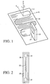
- With reference to Fig. 1, a portable, hand-held
scanning device 10 is shown as having followed a meanderingpath 12 along an original 14. The original may be a piece of paper, but the invention may be used with other image-bearing originals. In use of the hand-held scanning device, the positions of inherent structural features, such as paper fibers, may be tracked and the resulting positional information may be used to rectify image data. However, the system may be used in other applications, including integrated circuit fabrication. - The
scanning device 10 is preferably self-contained and battery operated. However, the device may include a connection to an external source of power or to data ports of computers or networks. The scanning device includes animage display 16. The display may provide almost immediate viewing of a captured image. The display is not critical. - The
scanning device 10 allows three degrees of freedom, with two being in translation and one in rotation. As shown in Fig. 1, the first degree is the side-to-side movement (X axis movement) along the original 14. The second degree of freedom is movement upwardly and downwardly along the original (Y axis movement). The third degree of freedom is the ability to operate the device with rotational misalignment of a linear array of image sensor elements relative to the edge of the original 14 (P misalignment as a result of Z axis movement). That is, it is not necessary to maintain the linear array of imaging elements perpendicular to the direction of device translation. - Referring now to Figs. 1 and 2, the
bottom side 18 of thescanning device 10 includes a pivotingmember 20 that aids in maintaining proper contact between the original 14 and animaging sensor 22.Navigation sensors - For reasons of physical compactness, the
imaging sensor 22 is preferably a contact image device, but for applications in which compactness is less of a concern or a smaller image is desired, sensors employing projection optics may be employed, with magnification less than unity. Contact imaging devices typically employ lenses sold under the trademark SELFOC, which is a federally-registered mark of Nippon Sheet Glass Company Limited. Less conventionally, contact imaging can be obtained using interleaved array elements of sources and proximal sensors, without any imaging lenses. Conventional imaging sensors for scanning applications may be used. The imaging sensor may be part of a unit that also includes an illumination source, illumination optics, and image transfer optics. - In Fig. 1, the meandering
path 12 is shown as having four and a fraction swaths, i.e., side-to-side passes across the original 14. Auseful imaging sensor 22 for most applications has a length within the range of 25 mm and 100 mm. The swaths should include regions of overlap, so that a stitching process may be used to produce a faithful representation of the scanned original. - The
scanning device 10 includes at least onenavigation sensor imaging sensor 22. Thenavigation sensors scanning device 10 relative to the original. - Each navigation sensor is an array of photoelements that is formed on an integrated circuit substrate that includes readout and signal processing circuitry. The position accuracy necessary over the range of a pixel distance of 40 µm is 2.0 µm. The very high positional accuracy requires individual photoelements that are no larger than tens of micrometres in length in order to acquire sufficiently differing signals from element to element. In the preferred embodiment, the pixel size desired on the
paper original 14 is 40µm and a magnification of 1.5 is achieved by the imaging optics, so that the photoreceptor elements of thenavigation sensors µm X 60 µm. - Fig. 3 is a block diagram of circuitry to be preferably formed in a single integrated circuit chip. The chip is an analog signal processing chip designed to acquire and process two-dimensional images, providing cross-correlation information to an external controller, not shown. In the embodiment described above, the controller uses the image cross-correlation values to derive X-Y position information. The X-Y position information is then used to accurately reconstruct a linear image from the image data acquired using
imaging sensor 22 in Fig. 2. - In the embodiment of Fig. 3, the
navigation sensor 24 is an array having thirty-two rows and sixty-eight columns of photoelements. An array of sixty-eightcolumn transfer amplifiers 17 transfers signals in a row-to-row fashion from thenavigation sensor 24 to an array of sixty-fourDC removal circuits 19. In a cost-efficient image-capture system, it is difficult to illuminate a target area with perfectly consistent light intensity across the entire area to be imaged. The ability to provide uniform illumination is often proportional to the cost of the optics and the light source. Moreover, in the absence of cell-by-cell calibration of a conventional integrated light sensor, some variations in sensitivity will occur as a result of limitations of integrated circuit processing technology. In the navigation system for use with the analog signal processing chip of Fig. 3, it is required that cross-correlations be calculated between an incident image and an image captured previously at a different location relative to an imaging array. Any variations in illumination and photoelement sensitivity will degrade the correlation signal. Consequently, the spatialDC removal circuits 19 of Fig. 3 have been designed to maintain the integrity of the correlation signals, while keeping the cost of the system relatively low. Low spatial frequency changes in illumination and photoelement sensitivity which would otherwise corrupt the correlation signal are removed from the navigation image. Acomputational array 21 receives data from theDC removal circuits 19 and performs computations on the data before transferring across-correlation output 23 to the off-chip controller. Also shown in Fig. 3 is asource 25 of control logic for the various components of the chip. - An understanding of the operation of the
DC removal circuits 19 is not critical to a full understanding of the operation of thecomputational array 21, and is therefore not described in detail. However, it is useful to understand the basic operation of thecolumn transfer amplifiers 17. - Referring to Fig. 4, five
columns rows separate transfer amplifier read switch 60. In the operation of the circuitry of Fig. 4, no two photoelements are connected to the same transfer amplifier simultaneously. - Each transfer amplifier 50-58 operates as an integrator and includes an
input 62 that is connected to a source of a fixed voltage. Asecond input 64 is capacitively connected to theoutput 66 of the transfer amplifier by atransfer capacitor 68. - In the operation of the circuit of Fig. 4, the read switches of the
first row 38 of photoelements may be closed, so that eachtransfer capacitor 68 receives a charge corresponding to the light energy that is received at the associated photoelement in the first row. The received charge is transferred to subsequent processing circuitry via the output lines 66. The readout of a single row is estimated to be between 200 ns and 300 ns. Following the readout of the first row, the read switches of the first row are opened and the transfer amplifiers are reset. The read switches of thesecond row 40 are then closed in order to transfer the signals from the photoelements of the second row. The process is repeated until each row of photoelements is read. - By the operation of the transfer amplifiers 50-58 of Fig. 4, photoelement signals are transferred in a row-by-row fashion to subsequent circuitry. The
DC removal circuits 19 of Fig. 3 continue the parallel processing of photoelement signals, as established by the column transfer amplifiers. The DC removal circuits output sixty-four signals and are representative of light energy received at thenavigation sensor 24. In the embodiment of Fig. 3, a frame of signals is comprised of pixel values at the computational array, with the pixel values being acquired by thirty-two transfers of sixty-four signals from the DC removal circuits. - Fig. 5 illustrates the steps for carrying out the invention for tracking relative movement between a device and a region of interest. While the invention will be described with reference to processing photoelement signals indicative of images of inherent structural features such as paper fibers of a sheet of paper, the method is not restricted to any one application.
- The steps of Fig. 5 are performed to correlate successive frames of navigation information. In effect, the correlations compare the positions of imaged features in successive frames to provide information related to the position of the navigation sensor at a particular time. In the application of the process to scanners, the detection of correlations is then used to process image data generated by the
imaging sensor 22 to accurately represent the original. - In a
first step 70, a reference frame of signals is acquired. The reference frame may be considered to be a start position. The position of a navigation sensor relative to an imaged region at a later time may be determined by acquiring 72 a sample frame of signals from the navigation sensor at the later time and then computing correlation values 74 with respect to the reference frame and the later-acquired sample frame. - Acquiring the
initial reference frame 70 may take place upon initiation of the imaging process. For example, the acquisition may be triggered by mere placement of the scanning device into contact with the original. Alternatively, the scanning device may include a start button that initiates the image process and the navigation process. - While the navigation processing is performed computationally, the concepts of this embodiment may be described with reference to the conceptual view of Fig. 6. A
reference frame 76 of 7×7 pixels is shown as having an image of a T-shaped inherentstructural feature 78. At a later time (dt) a navigation sensor acquires asample frame 80 which is displaced with respect to frame 76, but which shows substantially the same inherent structural features. The duration dt is preferably set such that the relative displacement of the T-shapedfeature 78 is less than one pixel of the navigation sensor at the velocity of translation of the scanning device. This relative displacement is referred to herein as a "microstep." - If the scanning device has moved during the time period between acquiring the
reference frame 76 of signals and acquiring thesample frame 80 of signals, the T-shaped feature will be shifted. While the preferred embodiment is one in which dt is less than the time that allows a full-pixel movement, the conceptual representation of Fig. 6 shows that thefeature 78 has shifted upwardly and to the right by one full pixel. The full-pixel shift is assumed only to simplify the representation. -
Member 82 in Fig. 6 represents sequential shifts of a pixel value of a particular pixel within the 7×7 array offrame 80. The sequential shifts are individual offsets into the eight nearest-neighbor pixels. That is, step "0" does not include a shift, step "1" is a diagonal shift upward and to the left, step "2" is an upward shift, etc. The shifts are performed simultaneously for all of the pixels of thesample frame 80. In this manner, the nine pixel-shifted frames can be combined with thereference frame 76 to produce thearray 84 of position frames. The position frame designated as "Position 0" does not include a shift, so that the result is merely a combination offrames Position 7" has the minimum number of shaded pixels, and therefore is the frame with the highest correlation. Based upon the correlation results, the position of the T-shapedfeature 78 in thesample frame 80 is determined to be a diagonal rightward and upward shift relative to the position of the same feature in earlier-acquiredreference frame 76, which implies that the scanning device has moved leftwardly and downwardly during time dt. - While other correlation approaches may be employed, an acceptable approach is a "sum of the squared differences" correlation. For the embodiment of Fig. 6, there are nine correlation coefficients (Ck = C0, C1 ... C8) formed from the nine offsets at
member 82. Another option regards the shifting of thesample frame 80, since the correlation operates equally well by offsetting thereference frame 76 and leaving the sample frame unshifted. - Correlations are used to find the locations of
identical features 78 insuccessive frames - As previously noted, the frame-to-frame correlations are referred to as "microsteps," since frame acquisition rates are chosen to be sufficiently high to ensure that the displacements do not exceed the dimension of a single pixel. Referring to Fig. 5, a
determination 86 of whether to replace the reference frame prior to subsequent correlation processing is made following each computation of the correlation values atstep 74. If it is determined that the reference frame is not to be replaced, a determination is made atstep 88 as to whether to translate the signals, i.e., the pixel values, of the reference frame. If the T-shapedfeature 78 of Fig. 6 has been displaced by a full pixel value from the acquisition of thereference frame 76 to the acquisition of thesample frame 80, the pixel values of thereference frame 76 may be shifted upwardly and to the right to form a translated reference frame. This is shown atstep 90 in Fig. 5. The shifted reference frame may then be compared to a new sample frame acquired atstep 72. The decision not to translate the pixel values will be made when the imaged feature has undergone a relative displacement of only a small portion of the pixel distance. - Returning to step 86, if the determination is made to replace the reference frame, the
sample reference frame 80 in Fig. 6 becomes the new reference frame, as shown atstep 92 in Fig. 5. A new sample frame is then acquired atstep 72 and the process continues. While the process provides a high degree of correlation match, any errors that do occur will accumulate if the reference frame is not periodically replaced, but is instead periodically shifted atstep 90. In order to place a restriction on the growth rate of this "random walk" error, a new reference frame is acquired atstep 92. Merely as an example, the reference frame may be systematically replaced before any fifth shift can occur atstep 90. - Based upon the tracking of movement of the imaged features, the relative movement between the photoreceiver array and the region being imaged may be tracked. In the application of the system to a
scanning device 10 as shown in Figs. 1 and 2, this navigation information can then be used to arrange the image information from theimaging sensor 22, so as to provide a faithful representation of the image of the original. In one form of the arranging of the image information, the navigation information may be used to position-tag the image information. - Fig. 7 is a schematic diagram of an individual cell within the
computational array 21 of Fig. 3. However, as will be understood by persons skilled in the art, other circuits may be used to carry out the process steps described with reference to Figs. 5 and 6. - Image data WDATA(i) is representative of light energy from a particular photoelement loaded into the
computational cell 94 atline 96, with a charge compensatedtransistor switch 98 under the control of a WR(j) signal. After the WR(j) signal is deasserted, the new data is held oncapacitor 100 and is buffered by anamplifier 102. The computational cell is a data cell within a two-dimensional array of cells. Referring briefly to Fig. 6, the cell may be used to store pixel values and to shift the pixel values for a single pixel in the 7×7 array that comprisesframes CDATA node 104 of Fig. 7 is one CDATA node within the computational array that permits simultaneous signal processing of all pixels of a frame of signals. Initially, the array of CDATA nodes collectively forms the comparison image, or "reference frame." As will be explained below, the CDATA nodes subsequently form the sample frame.Control input CDOUT 106 selects signal CDATA, comparison data, or selects REFOUT for the nearest-neighbor output node NN(0) 108. - The nearest-neighbor inputs NN(0)-NN(8) 108, 112, 114, 116, 118, 120, 122, 124 and 126 are separately selected by means of switch control signals S(0)-S(8) on
lines 128. The NN(0)-NN(8) inputs 108-126 are the outputs of the nearest-neighbor cells according to thepixel map 82 of Fig. 6. Consequently, thenode 108 is shown both as an output that fans out for connection to nearest-neighbor cells and as an input for thecell 94. The switch control signals are generated by a 4-9 encoder, not shown, that is external to the computational array. The 4-bit input to the encoder is referred to as the nearest-neighbor address and takes on binary values from 0000(0) to 1000(8). - The nearest-neighbor input (NNINPUT)
node 130 is sampled by pulsingREFLD 132, thereby storing the NNINPUT onnode REFH 134. Similarly,REFDATA 136 can be sampled and held onREFSH 138 by pulsingREFSFT 140. - For testing,
ROWTSTB 142 can be asserted, allowing the NN(0) signal to propagate to theTEST output 144. The TEST signals from each cell in a row of cells connect to common vertical buses in each column of the computational array and are multiplexed at the bottom of the array and driven off-chip. A standard row decoder along the left edge of the array allows selection of a particular row for test. However, the test feature is not critical to the system. - Each
computation cell 94 in the array of cells has acircuit 146 that determines the correlation values identified in Fig. 5 with reference to step 74. Afirst input 148 receives the reference data fromREFDATA node 136. Asecond input 150 provides the nearest-neighbor input NNINPUT selected by the appropriate switch control signal atlines 128. Theoutput 152 of the correlation cell is a current. All of the correlation outputs in the computational array are summed together in a single off-chip summing resistor of atracking circuit 154. The voltage developed across the summing resistor is referred to as the correlation values in Fig. 5. - In the embodiment of Fig. 7, the
circuit 146 is based on a squared-difference calculation. Thecell 94 may be modified to provide product-based correlations without modifying the basic architecture of the array. Control inputs S(0)-S(8), REFLD, REFSFT and CDOUT are global to the entire array. - It is important to understand the relationship between the nearest-neighbor map represented by 82 in Fig. 6 for a single cell and for the array as a whole.
Location 0 of an image refers to the present location of the image. When referring to the movement of an image fromlocation 0 tolocation 1, the representation is that the image signals in all of the cells of the array are moved to the neighbor cell that is to the left and upward. That is, the movement is relevant to a single cell in the computational array and is relevant to every cell in the array. - The computational array functionality can be best described in terms of four basic operations: image acquisition, reference image load, correlation computation, and reference image translation. The image acquisition refers to the loading of new image signals via the
WDATA line 96 of eachcomputation cell 94. In the preferred implementation, every 40 Ts a new frame of signals, i.e., pixel values, is acquired from the photoelement array via the column transfer amplifiers and the DC removal amplifiers. - The process of loading a new image is referred to as a "frame transfer." Frame transfer takes approximately 10 Ts to complete. The frame transfer control circuit asserts a signal FTB, not shown, during frame transfer. The operations of the computation array described below are coordinated with the frame transfer process by observing and synchronizing with the FTB signal. The validity of a new comparison image is signaled by the falling edge of the FTB signal. The operations described below are only appropriate when FTB is not asserted.
- Loading a reference frame of pixel values is required before any image correlations can be calculated. To load the reference frame, all of the signals at the
CDATA nodes 104 in the computational array must be transferred to theREFH nodes 134. This is accomplished by settingCDOUT 106 and S(0) high, and pulsing the REFLD signal online 132. The reference frame can also be loaded from another nearest-neighbor location by asserting one of the S(1)-S(8) inputs instead of S(0).Amplifier 156 buffers theREFH node 134 from theREFDATA nodes 136. The two-dimensional array ofREFDATA nodes 136 within the computational array are then collectively known as the reference frame. - After a reference frame has been loaded, the computational array is ready to compute correlations. Correlations between the reference frame of pixel values and the subsequent sample frame are computed by setting the nearest-neighbor address to the desired value and recording the resulting voltage developed across the summing resistor of the
displacement tracking circuit 154. When the photoreceiver array has moved a single pixel distance from the location at which the reference frame was acquired, a strong correlation will be detected at one of the nearest-neighbor locations, since there will be a minimal level of output current. In Fig. 6, the correlation is detected to be atPOSITION 7 in thearray 84. Sub-pixel movements can be determined by interpolating from multiple current-output readings in two-dimensional correlation space. - It should be noted that correlations between the reference frame and itself can be computed by setting
CDOUT 106 low and pulsingREFSFT 140. This causes the nearest-neighbor inputs to come from the reference frame, rather than from the sample frame. - Fig. 5 referred to the
step 90 of shifting the reference frame. Navigational accuracy may be improved if a single reference frame can be used for multiple pixel movements of the photoreceiver array relative to the imaged region of interest. Due to constraints in the availability of routing area within the computational array, providing inter-cell connectivity other than with nearest-neighbor computation cells is impractical. However, to use the same reference frame for multiple pixel movements requires the ability to "reach" beyond the nearest-neighbor cells. This problem is solved with the reference frame shift atstep 90. - Upon detection that the relative movement between the navigation sensor and the imaged region of interest equals or exceeds one pixel distance, the reference frame is shifted to the new location within the computational array. The shift to the new location is coincident with the detected relative movement. With the reference frame in the new location, nearest-neighbor correlations become correlations between the translated reference frame and a newly acquired sample frame. By translating the pixel values of the reference frame to new locations, inter-cell connectivity is kept to a minimum without compromising navigational accuracy.
- The translation of the reference frame, identified at
step 90 in Fig. 5, is accomplished among the individual computation cells of the computational array. Referring to thecomputation cell 94 of Fig. 7, a first step is topulse REFSFT 140 high to sample-and-hold theREFDATA signal 136 atREFSH 138. Athird buffer amplifier 158 drivesREFOUT 160 with the REFSH signal.CDOUT 106 is driven low, allowingREFOUT 160 to be the output of thecomputation cell 94 at the NN(0)node 108. - The nearest-neighbor address is then set to select the appropriate S(0)-S(8) input from the switch control signal lines 128. For example, if the T-shaped
feature 78 in Fig. 6 is detected to have moved to the right and upwardly from the time at which thereference frame 76 is acquired to the time at which thesample frame 80 is acquired, the pixel values that comprise the reference frame must be shifted from cell-to-cell to the right and upwardly. Since S(0)-S(8) signals switch the address of thecell input NNINPUT 130, S(7) must be driven high to enable movement of the pixel value fromlocation 7 of 82 in Fig. 6 tolocation 0. This takes place in each computation cell of the computational array. AfterREFOUT 160 has settled on theNNINPUT 130 of the appropriate neighbor cell,REFLD 132 is pulsed high to sample-and-hold the translated reference values atREFH 134. After this operation has occurred in each of the computation cells of the array, the computational array is again ready to compute correlations.
Claims (10)
- A method of tracking relative movement between a device (10) and a region (14) of interest, the method comprising steps of:based on said correlation outputs generated in said correlating step, determining (154) a relative movement between said device and said region of interest between said first specific time and said second specific time.fixing a two-dimensional array (24) of photoelements to said device such that each photoelement generates an output responsive to light energy received at said photoelement from said region of interest;deriving (70 and 72) frames of signals from the outputs from said array of photoelements at specific times, such that said signals in each said frame have a correspondence with said photoelements in said array, including limiting a duration between deriving successive frames to a time span in which anticipated said relative movement is less than a length of one of said photoelements, said step of deriving including successively deriving a first frame (76) of said signals at a first specific time and deriving a second frame (80) of said signals at a second specific time;enabling correlation signal-generating circuits for correlating (74) said signals of said first frame to said signals of said second frame to determine relative movement between said device and said region of interest, including substeps of:(a) selecting (82) signals from said first frame in a shifted relationship (84) to a specific signal of said second frame such that each said signal selected from said first frame is offset from said specific signal of said second frame by a shift amount, said shift amount having a correspondence with a shift of a single photoelement within said array of photoelements, so that said signals from said first frame correspond to those photoelements of said array that are immediately adjacent to said photoelement that corresponds to said specific signal of said second frame,(b) generating correlation outputs (152) responsive to correlations between said signals selected from said first frame in substep (a) and said specific signal, including generating each said correlation output from a different said correlation signal-generating circuit, thereby generating a correlation output for a plurality of shift directions relative to said photoelement that corresponds to said specific signal of said second frame, and(c) repetitively executing substeps (a) and (b) to generate correlation outputs for each of a plurality of said signals from said second frame; and
- A method as in claim 1, wherein said substep (c) of repetitively executing substeps (a) and (b) includes selecting (82) eight shift directions relative to an unshifted position, thereby generating (74) at least eight correlation outputs.
- A method as in claim 1 or 2, wherein said step of deriving (70 and 74) said frames (76 and 80) is a step of capturing frames of pixel values indicative of light energy received at said photoelements at said specific times.
- A method as in claim 3, wherein said step of correlating (74) said signals of said first and second frames includes repetitively translating said captured second frame (80) of pixel values relative to said captured first frame (76) of pixel values, thereby enabling generation (74) of one of said correlation outputs for each translation.
- A method as in any preceding claim, comprising the steps of storing said first frame (76) and correlating said signals of said stored first frame to signals of a plurality of frames (80) derived after said first frame, wherein each of said substeps (a), (b) and (c) is executed for each correlation.
- A method as in any preceding claim, wherein said step of fixing said two-dimensional array to said device is a step of fixing a navigation sensor array (24) to a scanner (10) having an image array (22) of photoelements.
- A device able to track its movement relative to a region of interest, comprising:a navigation sensor (24) including a two-dimensional array of photoelements responsive to reception of light energy;first circuit means (50, 52, 54, 56 and 58) for deriving frames (76 and 80) of signals in which each signal in a frame is indicative of light energy received at an individual photoelement at a specific time, and operable to output said signals, each of said signals corresponding to one photoelement of said array; andsecond circuit means (94), connected to said first circuit means, for correlating first and second frames of said signals output from said first circuit means to determine relative movement between said device and said region of interest, said second circuit means including an array of correlation signal-generating circuits (146) in one-to-one correspondence with said signals, each correlation-signal generating circuit being operable to receive (148) the signal corresponding to an individual photoelement of said array and being selectively connectable to receive (150) the signals corresponding to other photoelements immediately adjacent to said individual photoelement in said array, each correlation-signal generating circuit being operable to generate a correlation signal output (152) responsive to said signal corresponding to said individual photoelement and to said signals corresponding to said other photoelements.
- A device as in claim 7, comprising an image sensor (22) in fixed relation to said navigation sensor (24), said image sensor including a plurality of photoelements for forming image information of said region of interest.
- A device as in claim 8, comprising means (154) for position-tagging said image information based upon said outputs (152) from said correlation output circuits (146).
- A device as in claim 7, 8 or 9, wherein said correlation signal-generating circuits (146) include difference-squared circuits, each including a first input (148) from said individual photoelement of said array and a second input (150) sequentially connected to said other photoelements.
Applications Claiming Priority (2)
| Application Number | Priority Date | Filing Date | Title |
|---|---|---|---|
| US08/591,847 US5729008A (en) | 1996-01-25 | 1996-01-25 | Method and device for tracking relative movement by correlating signals from an array of photoelements |
| US591847 | 1996-01-25 |
Publications (3)
| Publication Number | Publication Date |
|---|---|
| EP0786892A2 EP0786892A2 (en) | 1997-07-30 |
| EP0786892A3 EP0786892A3 (en) | 1998-07-29 |
| EP0786892B1 true EP0786892B1 (en) | 2003-04-02 |
Family
ID=24368200
Family Applications (1)
| Application Number | Title | Priority Date | Filing Date |
|---|---|---|---|
| EP97300126A Expired - Lifetime EP0786892B1 (en) | 1996-01-25 | 1997-01-10 | Method and device for tracking relative movement |
Country Status (4)
| Country | Link |
|---|---|
| US (1) | US5729008A (en) |
| EP (1) | EP0786892B1 (en) |
| JP (1) | JPH09214691A (en) |
| DE (1) | DE69720306T2 (en) |
Families Citing this family (167)
| Publication number | Priority date | Publication date | Assignee | Title |
|---|---|---|---|---|
| USRE42918E1 (en) | 1994-01-28 | 2011-11-15 | California Institute Of Technology | Single substrate camera device with CMOS image sensor |
| US6456326B2 (en) | 1994-01-28 | 2002-09-24 | California Institute Of Technology | Single chip camera device having double sampling operation |
| US5471515A (en) | 1994-01-28 | 1995-11-28 | California Institute Of Technology | Active pixel sensor with intra-pixel charge transfer |
| US5578813A (en) * | 1995-03-02 | 1996-11-26 | Allen; Ross R. | Freehand image scanning device which compensates for non-linear movement |
| US5786804A (en) * | 1995-10-06 | 1998-07-28 | Hewlett-Packard Company | Method and system for tracking attitude |
| US6950094B2 (en) * | 1998-03-30 | 2005-09-27 | Agilent Technologies, Inc | Seeing eye mouse for a computer system |
| US6345116B1 (en) * | 1996-05-31 | 2002-02-05 | Matsushita Electric Industrial Co., Ltd. | Image processing apparatus |
| EP0873003B1 (en) | 1997-04-14 | 2007-03-21 | Hewlett-Packard Company, A Delaware Corporation | Image scanning device and method |
| US6256016B1 (en) | 1997-06-05 | 2001-07-03 | Logitech, Inc. | Optical detection system, device, and method utilizing optical matching |
| DE69816185T2 (en) | 1997-06-12 | 2004-04-15 | Hewlett-Packard Co. (N.D.Ges.D.Staates Delaware), Palo Alto | Image processing method and device |
| US6002124A (en) * | 1998-03-20 | 1999-12-14 | Hewlett-Packard Company | Portable image scanner with optical position sensors |
| US6097851A (en) * | 1998-03-31 | 2000-08-01 | Agilent Technologies | Low latency correlation |
| US6069351A (en) * | 1998-07-16 | 2000-05-30 | Intel Corporation | Focal plane processor for scaling information from image sensors |
| JP2000069243A (en) * | 1998-08-24 | 2000-03-03 | Matsushita Electric Ind Co Ltd | Image processing method and image processor |
| US6195475B1 (en) * | 1998-09-15 | 2001-02-27 | Hewlett-Packard Company | Navigation system for handheld scanner |
| US6118132A (en) * | 1998-09-17 | 2000-09-12 | Agilent Technologies | System for measuring the velocity, displacement and strain on a moving surface or web of material |
| US6188058B1 (en) | 1998-09-17 | 2001-02-13 | Agilent Technologies Inc. | System for taking displacement measurements having photosensors with imaged pattern arrangement |
| US6403941B1 (en) | 1998-10-29 | 2002-06-11 | Hewlett-Packard Company | Image scanner with real time pixel resampling |
| US6222174B1 (en) | 1999-03-05 | 2001-04-24 | Hewlett-Packard Company | Method of correlating immediately acquired and previously stored feature information for motion sensing |
| US6246050B1 (en) | 1999-03-08 | 2001-06-12 | Hewlett-Packard Company | Optical encoders using non-patterned targets |
| US6633332B1 (en) * | 1999-05-13 | 2003-10-14 | Hewlett-Packard Development Company, L.P. | Digital camera system and method capable of performing document scans |
| US6207945B1 (en) * | 1999-06-30 | 2001-03-27 | Hewlett-Packard Company | Integral positioning and imaging device |
| US6229297B1 (en) * | 1999-06-30 | 2001-05-08 | Hewlett-Packard Company | Device for determining the position of an object relative to a surface |
| US6265706B1 (en) * | 1999-07-12 | 2001-07-24 | Hewlett-Packard Company | Edge to edge image sensor and navigator for portable scanner |
| US6556315B1 (en) | 1999-07-30 | 2003-04-29 | Hewlett-Packard Company | Digital image scanner with compensation for misalignment of photosensor array segments |
| US6312124B1 (en) | 1999-10-27 | 2001-11-06 | Hewlett-Packard Company | Solid and semi-flexible body inkjet printing system |
| US6455840B1 (en) | 1999-10-28 | 2002-09-24 | Hewlett-Packard Company | Predictive and pulsed illumination of a surface in a micro-texture navigation technique |
| US6568777B1 (en) * | 1999-11-16 | 2003-05-27 | Agilent Technologies, Inc. | Optical navigation system and method |
| US6303921B1 (en) | 1999-11-23 | 2001-10-16 | Hewlett-Packard Company | Method and system for capturing large format documents using a portable hand-held scanner |
| US6563101B1 (en) | 2000-01-19 | 2003-05-13 | Barclay J. Tullis | Non-rectilinear sensor arrays for tracking an image |
| US6529184B1 (en) | 2000-03-22 | 2003-03-04 | Microsoft Corporation | Ball pattern architecture |
| US7161578B1 (en) | 2000-08-02 | 2007-01-09 | Logitech Europe S.A. | Universal presentation device |
| US7289649B1 (en) | 2000-08-10 | 2007-10-30 | Avago Technologies Ecbu Ip (Singapore) Pte. Ltd. | Fingerprint imager |
| US6781570B1 (en) | 2000-11-09 | 2004-08-24 | Logitech Europe S.A. | Wireless optical input device |
| US20030098352A1 (en) * | 2000-11-24 | 2003-05-29 | Metrologic Instruments, Inc. | Handheld imaging device employing planar light illumination and linear imaging with image-based velocity detection and aspect ratio compensation |
| US7164810B2 (en) * | 2001-11-21 | 2007-01-16 | Metrologic Instruments, Inc. | Planar light illumination and linear imaging (PLILIM) device with image-based velocity detection and aspect ratio compensation |
| US7333083B1 (en) | 2001-05-10 | 2008-02-19 | Logitech Europe S.A. | Optical based performance improvement for an optical illumination configuration |
| US6664948B2 (en) * | 2001-07-30 | 2003-12-16 | Microsoft Corporation | Tracking pointing device motion using a single buffer for cross and auto correlation determination |
| US6847353B1 (en) | 2001-07-31 | 2005-01-25 | Logitech Europe S.A. | Multiple sensor device and method |
| TW530489B (en) * | 2001-09-11 | 2003-05-01 | Pixart Imaging Inc | Moving distance detection method of image sensor |
| US7343049B2 (en) * | 2002-03-07 | 2008-03-11 | Marvell International Technology Ltd. | Method and apparatus for performing optical character recognition (OCR) and text stitching |
| US6788875B1 (en) | 2002-04-08 | 2004-09-07 | Logitech Europe S.A. | Suspension system for use in an optical displacement detection system |
| US7131751B1 (en) | 2002-04-12 | 2006-11-07 | Logitech, Inc. | Attachment system for use in an optical illumination system |
| US7045763B2 (en) * | 2002-06-28 | 2006-05-16 | Hewlett-Packard Development Company, L.P. | Object-recognition lock |
| US6983080B2 (en) * | 2002-07-19 | 2006-01-03 | Agilent Technologies, Inc. | Resolution and image quality improvements for small image sensors |
| DE10254614B4 (en) * | 2002-11-22 | 2006-04-20 | Infineon Technologies Ag | Method for detecting a relative movement of a finger relative to a sensor surface |
| US7275292B2 (en) * | 2003-03-07 | 2007-10-02 | Avago Technologies Wireless Ip (Singapore) Pte. Ltd. | Method for fabricating an acoustical resonator on a substrate |
| EP1613476A4 (en) * | 2003-03-31 | 2010-03-17 | Segan Ind Inc | Direct remote analog/digit printing devices, processes and mediums |
| US7164782B2 (en) * | 2003-04-18 | 2007-01-16 | Avago Technologies Ecbu Ip (Singapore) Pte. Ltd. | System and method for time-space multiplexing in finger-imaging applications |
| US7158659B2 (en) * | 2003-04-18 | 2007-01-02 | Avago Technologies Ecbu Ip (Singapore) Pte. Ltd. | System and method for multiplexing illumination in combined finger recognition and finger navigation module |
| US7274808B2 (en) * | 2003-04-18 | 2007-09-25 | Avago Technologies Ecbu Ip (Singapore)Pte Ltd | Imaging system and apparatus for combining finger recognition and finger navigation |
| US6751410B1 (en) | 2003-07-10 | 2004-06-15 | Hewlett-Packard Development Company, L.P. | Inertial camera stabilization apparatus and method |
| FR2857768B1 (en) * | 2003-07-18 | 2006-01-06 | Atmel Grenoble Sa | METHOD FOR ACQUIRING DIGITAL FOOTPRINT IMAGE |
| JP2005041623A (en) * | 2003-07-25 | 2005-02-17 | Fuji Xerox Co Ltd | Carrying device and image forming device |
| US20050024690A1 (en) * | 2003-07-31 | 2005-02-03 | Picciotto Carl E. | Pen with tag reader and navigation system |
| US20050135659A1 (en) * | 2003-12-19 | 2005-06-23 | Smith John D. | Optical motion sensor |
| US7268341B2 (en) * | 2004-05-21 | 2007-09-11 | Silicon Light Machines Corporation | Optical position sensing device including interlaced groups of photosensitive elements |
| US20050259078A1 (en) * | 2004-05-21 | 2005-11-24 | Silicon Light Machines Corporation | Optical positioning device with multi-row detector array |
| US20050259097A1 (en) * | 2004-05-21 | 2005-11-24 | Silicon Light Machines Corporation | Optical positioning device using different combinations of interlaced photosensitive elements |
| US7042575B2 (en) * | 2004-05-21 | 2006-05-09 | Silicon Light Machines Corporation | Speckle sizing and sensor dimensions in optical positioning device |
| US7773070B2 (en) | 2004-05-21 | 2010-08-10 | Cypress Semiconductor Corporation | Optical positioning device using telecentric imaging |
| US7285766B2 (en) * | 2004-05-21 | 2007-10-23 | Silicon Light Machines Corporation | Optical positioning device having shaped illumination |
| US20050258346A1 (en) * | 2004-05-21 | 2005-11-24 | Silicon Light Machines Corporation | Optical positioning device resistant to speckle fading |
| US8532338B2 (en) * | 2004-07-06 | 2013-09-10 | Hewlett-Packard Development Company, L.P. | System and method for compensating for motion blur in optical navigation |
| EP1615045A1 (en) * | 2004-07-07 | 2006-01-11 | STMicroelectronics Limited | Optical detection of relative motion |
| US7349588B2 (en) * | 2004-08-25 | 2008-03-25 | Avago Technologies Ecbu Ip Pte Ltd | Automatic meter reading |
| US7388454B2 (en) * | 2004-10-01 | 2008-06-17 | Avago Technologies Wireless Ip Pte Ltd | Acoustic resonator performance enhancement using alternating frame structure |
| US7138620B2 (en) * | 2004-10-29 | 2006-11-21 | Silicon Light Machines Corporation | Two-dimensional motion sensor |
| US7248345B2 (en) * | 2004-11-12 | 2007-07-24 | Silicon Light Machines Corporation | Signal processing method for use with an optical navigation system |
| US8981876B2 (en) | 2004-11-15 | 2015-03-17 | Avago Technologies General Ip (Singapore) Pte. Ltd. | Piezoelectric resonator structures and electrical filters having frame elements |
| WO2006068746A2 (en) | 2004-11-19 | 2006-06-29 | Silicon Light Machines Corporation | Dense multi-axis array for motion sensing |
| US7435942B2 (en) * | 2004-12-02 | 2008-10-14 | Cypress Semiconductor Corporation | Signal processing method for optical sensors |
| US7202560B2 (en) | 2004-12-15 | 2007-04-10 | Avago Technologies Wireless Ip (Singapore) Pte. Ltd. | Wafer bonding of micro-electro mechanical systems to active circuitry |
| US7791434B2 (en) * | 2004-12-22 | 2010-09-07 | Avago Technologies Wireless Ip (Singapore) Pte. Ltd. | Acoustic resonator performance enhancement using selective metal etch and having a trench in the piezoelectric |
| TWI254581B (en) * | 2004-12-27 | 2006-05-01 | Sunplus Technology Co Ltd | Method and device for detecting image movements |
| US7365856B2 (en) | 2005-01-21 | 2008-04-29 | Carl Zeiss Meditec, Inc. | Method of motion correction in optical coherence tomography imaging |
| US7805009B2 (en) * | 2005-04-06 | 2010-09-28 | Carl Zeiss Meditec, Inc. | Method and apparatus for measuring motion of a subject using a series of partial images from an imaging system |
| US7369013B2 (en) * | 2005-04-06 | 2008-05-06 | Avago Technologies Wireless Ip Pte Ltd | Acoustic resonator performance enhancement using filled recessed region |
| US7656428B2 (en) * | 2005-05-05 | 2010-02-02 | Avago Technologies General Ip (Singapore) Pte. Ltd. | Imaging device employing optical motion sensor as gyroscope |
| US7474848B2 (en) * | 2005-05-05 | 2009-01-06 | Hewlett-Packard Development Company, L.P. | Method for achieving correct exposure of a panoramic photograph |
| WO2007030731A2 (en) * | 2005-09-07 | 2007-03-15 | Nr Laboratories, Llc | Positional sensing system and method |
| US7598979B2 (en) * | 2005-09-21 | 2009-10-06 | Aptina Imaging Corporation | Imaging device with blur reduction system including a primary array and at least one navigation array |
| US20070076082A1 (en) * | 2005-09-30 | 2007-04-05 | Lexmark International, Inc. | Methods and apparatuses for measuring print area using hand-held printer |
| US7500732B2 (en) * | 2005-09-30 | 2009-03-10 | Lexmark International, Inc. | Maintenance and docking station for a hand-held printer |
| US7735951B2 (en) * | 2005-11-15 | 2010-06-15 | Lexmark International, Inc. | Alignment method for hand-operated printer |
| US20070120937A1 (en) * | 2005-11-30 | 2007-05-31 | Lexmark International, Inc. | System and method for hand-held printing |
| US7567235B2 (en) | 2005-12-12 | 2009-07-28 | Cypress Semiconductor Corporation | Self-aligning optical sensor package |
| US8471191B2 (en) * | 2005-12-16 | 2013-06-25 | Cypress Semiconductor Corporation | Optical navigation system having a filter-window to seal an enclosure thereof |
| US7765251B2 (en) * | 2005-12-16 | 2010-07-27 | Cypress Semiconductor Corporation | Signal averaging circuit and method for sample averaging |
| US7399129B2 (en) * | 2005-12-20 | 2008-07-15 | Lexmark International, Inc. | User interface for a hand-operated printer |
| US7524051B2 (en) * | 2005-12-20 | 2009-04-28 | Lexmark International, Inc. | Hand-operated printer having a user interface |
| US7737948B2 (en) | 2005-12-20 | 2010-06-15 | Cypress Semiconductor Corporation | Speckle navigation system |
| US7298460B2 (en) * | 2006-01-03 | 2007-11-20 | Silicon Light Machines Corporation | Method for determining motion using a velocity predictor |
| US7884801B1 (en) | 2006-02-16 | 2011-02-08 | Cypress Semiconductor Corporation | Circuit and method for determining motion with redundant comb-arrays |
| US7479685B2 (en) * | 2006-03-10 | 2009-01-20 | Avago Technologies General Ip (Singapore) Pte. Ltd. | Electronic device on substrate with cavity and mitigated parasitic leakage path |
| US7297912B1 (en) | 2006-03-27 | 2007-11-20 | Silicon Light Machines Corporation | Circuit and method for reducing power consumption in an optical navigation system having redundant arrays |
| US7809035B2 (en) * | 2006-03-31 | 2010-10-05 | Cypress Semiconductor Corporation | Eye-safe laser navigation sensor |
| US7721609B2 (en) | 2006-03-31 | 2010-05-25 | Cypress Semiconductor Corporation | Method and apparatus for sensing the force with which a button is pressed |
| US20070237561A1 (en) * | 2006-04-11 | 2007-10-11 | Lexmark International Inc. | Methods and apparatuses for sensing a print area using a hand-held printer |
| US8036428B2 (en) * | 2006-04-28 | 2011-10-11 | Pixart Imaging Inc. | Method and apparatus for detecting motion of image in optical navigator |
| US7748839B2 (en) | 2006-05-09 | 2010-07-06 | Lexmark International, Inc. | Handheld printing with reference indicia |
| US7682017B2 (en) * | 2006-05-10 | 2010-03-23 | Lexmark International, Inc. | Handheld printer minimizing printing defects |
| US7492445B1 (en) | 2006-06-05 | 2009-02-17 | Cypress Semiconductor Corporation | Method and apparatus for robust velocity prediction |
| US7755604B2 (en) | 2006-06-19 | 2010-07-13 | Cypress Semiconductor Corporation | Optical navigation sensor with tracking and lift detection for optically transparent contact surfaces |
| US7787145B2 (en) * | 2006-06-29 | 2010-08-31 | Lexmark International, Inc. | Methods for improving print quality in a hand-held printer |
| US7728816B2 (en) * | 2006-07-10 | 2010-06-01 | Cypress Semiconductor Corporation | Optical navigation sensor with variable tracking resolution |
| US20080030534A1 (en) * | 2006-08-02 | 2008-02-07 | Adam Jude Ahne | Hand Held Micro-fluid Ejection Devices Configured to Eject Fluid without Referential Position Information and Method of Ejecting Fluid |
| US20080079956A1 (en) * | 2006-09-21 | 2008-04-03 | Mahesan Chelvayohan | Hand-Held Printer Having An Integrated Digital Camera Scanner |
| US20080075513A1 (en) * | 2006-09-26 | 2008-03-27 | Douglas Laurence Robertson | Methods for a Maintenance Algorithm in Hand Held Printers |
| US7938531B2 (en) | 2006-09-27 | 2011-05-10 | Lexmark International, Inc. | Methods and apparatus for handheld printing with optical positioning |
| US7918519B2 (en) | 2006-09-27 | 2011-04-05 | Lexmark International, Inc. | Methods and apparatus for handheld printing with optical positioning |
| US7748840B2 (en) * | 2006-09-27 | 2010-07-06 | Lexmark International, Inc. | Methods and apparatus for handheld printing with optical positioning |
| US7742514B1 (en) | 2006-10-31 | 2010-06-22 | Cypress Semiconductor Corporation | Laser navigation sensor |
| US8072429B2 (en) * | 2006-12-22 | 2011-12-06 | Cypress Semiconductor Corporation | Multi-axial touch-sensor device with multi-touch resolution |
| US7938532B2 (en) | 2007-02-16 | 2011-05-10 | Lexmark International, Inc. | Hand held printer with vertical misalignment correction |
| US20080219737A1 (en) * | 2007-03-07 | 2008-09-11 | Michael David Stilz | Hand Held Printer Having A Doppler Position Sensor |
| US20080231714A1 (en) * | 2007-03-22 | 2008-09-25 | Texas Instruments Incorporated | System and method for capturing images |
| US8092006B2 (en) | 2007-06-22 | 2012-01-10 | Lexmark International, Inc. | Handheld printer configuration |
| US8314774B1 (en) | 2007-07-09 | 2012-11-20 | Cypress Semiconductor Corporation | Method and apparatus for quasi-3D tracking using 2D optical motion sensors |
| TWI374401B (en) * | 2007-07-09 | 2012-10-11 | Pixart Imaging Inc | Detection method for displacements with sub-pixel accuracy and apparatus using the same |
| US8263921B2 (en) | 2007-08-06 | 2012-09-11 | Cypress Semiconductor Corporation | Processing methods for speckle-based motion sensing |
| US20090040286A1 (en) * | 2007-08-08 | 2009-02-12 | Tan Theresa Joy L | Print scheduling in handheld printers |
| US8259069B1 (en) | 2008-01-11 | 2012-09-04 | Cypress Semiconductor Corporation | Speckle-based optical navigation on curved tracking surface |
| US8031176B1 (en) | 2008-01-22 | 2011-10-04 | Cypress Semiconductor Corporation | Optical navigation system using a single-package motion sensor |
| US8625934B2 (en) | 2008-01-28 | 2014-01-07 | Pixart Imaging Inc. | Method and apparatus for detecting displacement with sub-pixel accuracy |
| CN101257581A (en) * | 2008-03-26 | 2008-09-03 | 香港应用科技研究院有限公司 | Light sensation sensor and image catching device |
| US7855618B2 (en) * | 2008-04-30 | 2010-12-21 | Avago Technologies Wireless Ip (Singapore) Pte. Ltd. | Bulk acoustic resonator electrical impedance transformers |
| US7732977B2 (en) * | 2008-04-30 | 2010-06-08 | Avago Technologies Wireless Ip (Singapore) | Transceiver circuit for film bulk acoustic resonator (FBAR) transducers |
| US20100060592A1 (en) * | 2008-09-10 | 2010-03-11 | Jeffrey Traer Bernstein | Data Transmission and Reception Using Optical In-LCD Sensing |
| US8541727B1 (en) | 2008-09-30 | 2013-09-24 | Cypress Semiconductor Corporation | Signal monitoring and control system for an optical navigation sensor |
| US7723659B1 (en) | 2008-10-10 | 2010-05-25 | Cypress Semiconductor Corporation | System and method for screening semiconductor lasers |
| JP2010154088A (en) * | 2008-12-24 | 2010-07-08 | Seiko Epson Corp | Image processing matching position and image |
| US8217334B1 (en) | 2008-12-24 | 2012-07-10 | Cypress Semiconductor Corporation | Optical navigation sensor including a spatial frequency filter |
| JP2010161435A (en) * | 2009-01-06 | 2010-07-22 | Seiko Epson Corp | Document reading apparatus |
| US8711096B1 (en) | 2009-03-27 | 2014-04-29 | Cypress Semiconductor Corporation | Dual protocol input device |
| US8248185B2 (en) * | 2009-06-24 | 2012-08-21 | Avago Technologies Wireless Ip (Singapore) Pte. Ltd. | Acoustic resonator structure comprising a bridge |
| US8902023B2 (en) * | 2009-06-24 | 2014-12-02 | Avago Technologies General Ip (Singapore) Pte. Ltd. | Acoustic resonator structure having an electrode with a cantilevered portion |
| US8664548B2 (en) | 2009-09-11 | 2014-03-04 | Apple Inc. | Touch controller with improved diagnostics calibration and communications support |
| US9243316B2 (en) | 2010-01-22 | 2016-01-26 | Avago Technologies General Ip (Singapore) Pte. Ltd. | Method of fabricating piezoelectric material with selected c-axis orientation |
| US8796904B2 (en) | 2011-10-31 | 2014-08-05 | Avago Technologies General Ip (Singapore) Pte. Ltd. | Bulk acoustic resonator comprising piezoelectric layer and inverse piezoelectric layer |
| US9851849B2 (en) | 2010-12-03 | 2017-12-26 | Apple Inc. | Touch device communication |
| US8962443B2 (en) | 2011-01-31 | 2015-02-24 | Avago Technologies General Ip (Singapore) Pte. Ltd. | Semiconductor device having an airbridge and method of fabricating the same |
| US9154112B2 (en) | 2011-02-28 | 2015-10-06 | Avago Technologies General Ip (Singapore) Pte. Ltd. | Coupled resonator filter comprising a bridge |
| US9425764B2 (en) | 2012-10-25 | 2016-08-23 | Avago Technologies General Ip (Singapore) Pte. Ltd. | Accoustic resonator having composite electrodes with integrated lateral features |
| US9203374B2 (en) | 2011-02-28 | 2015-12-01 | Avago Technologies General Ip (Singapore) Pte. Ltd. | Film bulk acoustic resonator comprising a bridge |
| US9048812B2 (en) | 2011-02-28 | 2015-06-02 | Avago Technologies General Ip (Singapore) Pte. Ltd. | Bulk acoustic wave resonator comprising bridge formed within piezoelectric layer |
| US9148117B2 (en) | 2011-02-28 | 2015-09-29 | Avago Technologies General Ip (Singapore) Pte. Ltd. | Coupled resonator filter comprising a bridge and frame elements |
| US9083302B2 (en) | 2011-02-28 | 2015-07-14 | Avago Technologies General Ip (Singapore) Pte. Ltd. | Stacked bulk acoustic resonator comprising a bridge and an acoustic reflector along a perimeter of the resonator |
| US9136818B2 (en) | 2011-02-28 | 2015-09-15 | Avago Technologies General Ip (Singapore) Pte. Ltd. | Stacked acoustic resonator comprising a bridge |
| US9444426B2 (en) | 2012-10-25 | 2016-09-13 | Avago Technologies General Ip (Singapore) Pte. Ltd. | Accoustic resonator having integrated lateral feature and temperature compensation feature |
| US8575820B2 (en) | 2011-03-29 | 2013-11-05 | Avago Technologies General Ip (Singapore) Pte. Ltd. | Stacked bulk acoustic resonator |
| US9033510B2 (en) | 2011-03-30 | 2015-05-19 | Carl Zeiss Meditec, Inc. | Systems and methods for efficiently obtaining measurements of the human eye using tracking |
| US8350445B1 (en) | 2011-06-16 | 2013-01-08 | Avago Technologies Wireless Ip (Singapore) Pte. Ltd. | Bulk acoustic resonator comprising non-piezoelectric layer and bridge |
| WO2012173640A1 (en) | 2011-06-16 | 2012-12-20 | Cypress Semiconductor Corporaton | An optical navigation module with capacitive sensor |
| US8857988B2 (en) | 2011-07-07 | 2014-10-14 | Carl Zeiss Meditec, Inc. | Data acquisition methods for reduced motion artifacts and applications in OCT angiography |
| US8922302B2 (en) | 2011-08-24 | 2014-12-30 | Avago Technologies General Ip (Singapore) Pte. Ltd. | Acoustic resonator formed on a pedestal |
| US8896553B1 (en) | 2011-11-30 | 2014-11-25 | Cypress Semiconductor Corporation | Hybrid sensor module |
| US9101294B2 (en) | 2012-01-19 | 2015-08-11 | Carl Zeiss Meditec, Inc. | Systems and methods for enhanced accuracy in OCT imaging of the cornea |
| US10638221B2 (en) | 2012-11-13 | 2020-04-28 | Adobe Inc. | Time interval sound alignment |
| US9165373B2 (en) | 2013-03-11 | 2015-10-20 | Adobe Systems Incorporated | Statistics of nearest neighbor fields |
| US9031345B2 (en) | 2013-03-11 | 2015-05-12 | Adobe Systems Incorporated | Optical flow accounting for image haze |
| US9025822B2 (en) | 2013-03-11 | 2015-05-05 | Adobe Systems Incorporated | Spatially coherent nearest neighbor fields |
| US9129399B2 (en) * | 2013-03-11 | 2015-09-08 | Adobe Systems Incorporated | Optical flow with nearest neighbor field fusion |
| CN104340710A (en) * | 2013-07-26 | 2015-02-11 | 山东新北洋信息技术股份有限公司 | Slice medium moving state detection method and device and medium treatment device |
| US9562955B2 (en) | 2014-01-20 | 2017-02-07 | Qualcomm Incorporated | Methods and apparatus for magnetic field strength measurement |
| TWI568237B (en) * | 2015-07-29 | 2017-01-21 | 東友科技股份有限公司 | Image capture method and image capture and synthesis method |
| US11128636B1 (en) | 2020-05-13 | 2021-09-21 | Science House LLC | Systems, methods, and apparatus for enhanced headsets |
Family Cites Families (9)
| Publication number | Priority date | Publication date | Assignee | Title |
|---|---|---|---|---|
| US4133004A (en) * | 1977-11-02 | 1979-01-02 | Hughes Aircraft Company | Video correlation tracker |
| US4270143A (en) * | 1978-12-20 | 1981-05-26 | General Electric Company | Cross-correlation video tracker and method |
| US4882629A (en) * | 1987-05-08 | 1989-11-21 | Everex Ti Corporation | Adaptive exposure control system |
| US5089712A (en) * | 1989-06-08 | 1992-02-18 | Hewlett-Packard Company | Sheet advancement control system detecting fiber pattern of sheet |
| US4958224A (en) * | 1989-08-15 | 1990-09-18 | Hughes Aircraft Company | Forced correlation/mixed mode tracking system |
| US5184795A (en) | 1991-09-26 | 1993-02-09 | Sexton P Wayne | Manicure stand |
| US5149980A (en) * | 1991-11-01 | 1992-09-22 | Hewlett-Packard Company | Substrate advance measurement system using cross-correlation of light sensor array signals |
| US5216258A (en) * | 1992-03-09 | 1993-06-01 | Calcomp Inc. | Optical density tracking sensor for aligning media |
| US5578813A (en) * | 1995-03-02 | 1996-11-26 | Allen; Ross R. | Freehand image scanning device which compensates for non-linear movement |
-
1996
- 1996-01-25 US US08/591,847 patent/US5729008A/en not_active Expired - Lifetime
-
1997
- 1997-01-10 EP EP97300126A patent/EP0786892B1/en not_active Expired - Lifetime
- 1997-01-10 DE DE69720306T patent/DE69720306T2/en not_active Expired - Fee Related
- 1997-01-21 JP JP9008408A patent/JPH09214691A/en active Pending
Also Published As
| Publication number | Publication date |
|---|---|
| JPH09214691A (en) | 1997-08-15 |
| DE69720306D1 (en) | 2003-05-08 |
| US5729008A (en) | 1998-03-17 |
| DE69720306T2 (en) | 2004-03-04 |
| EP0786892A2 (en) | 1997-07-30 |
| EP0786892A3 (en) | 1998-07-29 |
Similar Documents
| Publication | Publication Date | Title |
|---|---|---|
| EP0786892B1 (en) | Method and device for tracking relative movement | |
| CN1912685B (en) | Imaging device employing optical motion sensor as gyroscope | |
| Ait-Aider et al. | Simultaneous object pose and velocity computation using a single view from a rolling shutter camera | |
| US6195475B1 (en) | Navigation system for handheld scanner | |
| US7598979B2 (en) | Imaging device with blur reduction system including a primary array and at least one navigation array | |
| US6037643A (en) | Photocell layout for high-speed optical navigation microchips | |
| US5644139A (en) | Navigation technique for detecting movement of navigation sensors relative to an object | |
| CN100380935C (en) | Image processing device and method, recording medium, and program | |
| US7340160B2 (en) | Imaging apparatus | |
| US5703353A (en) | Offset removal and spatial frequency band filtering circuitry for photoreceiver signals | |
| US4459619A (en) | Image reading apparatus | |
| US5917960A (en) | Image correlator, an image processing apparatus using the same, and a signal adder used in the image correlator | |
| US6903764B2 (en) | Image capturing apparatus, method for capturing image and camera | |
| US5850282A (en) | Distance measuring device | |
| JP2002359783A (en) | Imaging device and pixel defect correction method | |
| US5047845A (en) | Charge-transfer-device planar array for detecting coherent-light phase | |
| US6047136A (en) | Distance meter and an apparatus having a distance meter | |
| JP2000234925A (en) | Attitude detector | |
| Gottardi | A CMOS/CCD image sensor for 2D real time motion estimation | |
| JPH06225187A (en) | Image pickup device | |
| JP2643770B2 (en) | Imaging device | |
| JP3551670B2 (en) | Electronic still camera | |
| JP2522707B2 (en) | Image pickup device | |
| JP2657428B2 (en) | Image reading device | |
| JPH01237480A (en) | Acquisition and tracking apparatus for space craft |
Legal Events
| Date | Code | Title | Description |
|---|---|---|---|
| PUAI | Public reference made under article 153(3) epc to a published international application that has entered the european phase |
Free format text: ORIGINAL CODE: 0009012 |
|
| AK | Designated contracting states |
Kind code of ref document: A2 Designated state(s): DE FR GB |
|
| PUAL | Search report despatched |
Free format text: ORIGINAL CODE: 0009013 |
|
| AK | Designated contracting states |
Kind code of ref document: A3 Designated state(s): DE FR GB |
|
| 17P | Request for examination filed |
Effective date: 19981123 |
|
| RAP1 | Party data changed (applicant data changed or rights of an application transferred) |
Owner name: HEWLETT-PACKARD COMPANY, A DELAWARE CORPORATION |
|
| 17Q | First examination report despatched |
Effective date: 20010222 |
|
| RAP1 | Party data changed (applicant data changed or rights of an application transferred) |
Owner name: AGILENT TECHNOLOGIES, INC. (A DELAWARE CORPORATIO Owner name: HEWLETT-PACKARD COMPANY (A DELAWARE CORPORATION) |
|
| GRAH | Despatch of communication of intention to grant a patent |
Free format text: ORIGINAL CODE: EPIDOS IGRA |
|
| GRAH | Despatch of communication of intention to grant a patent |
Free format text: ORIGINAL CODE: EPIDOS IGRA |
|
| GRAA | (expected) grant |
Free format text: ORIGINAL CODE: 0009210 |
|
| AK | Designated contracting states |
Designated state(s): DE FR GB |
|
| PG25 | Lapsed in a contracting state [announced via postgrant information from national office to epo] |
Ref country code: FR Free format text: LAPSE BECAUSE OF FAILURE TO SUBMIT A TRANSLATION OF THE DESCRIPTION OR TO PAY THE FEE WITHIN THE PRESCRIBED TIME-LIMIT Effective date: 20030402 |
|
| REG | Reference to a national code |
Ref country code: GB Ref legal event code: FG4D |
|
| REF | Corresponds to: |
Ref document number: 69720306 Country of ref document: DE Date of ref document: 20030508 Kind code of ref document: P |
|
| PLBE | No opposition filed within time limit |
Free format text: ORIGINAL CODE: 0009261 |
|
| STAA | Information on the status of an ep patent application or granted ep patent |
Free format text: STATUS: NO OPPOSITION FILED WITHIN TIME LIMIT |
|
| EN | Fr: translation not filed | ||
| 26N | No opposition filed |
Effective date: 20040105 |
|
| PGFP | Annual fee paid to national office [announced via postgrant information from national office to epo] |
Ref country code: GB Payment date: 20070125 Year of fee payment: 11 |
|
| PGFP | Annual fee paid to national office [announced via postgrant information from national office to epo] |
Ref country code: DE Payment date: 20070228 Year of fee payment: 11 |
|
| GBPC | Gb: european patent ceased through non-payment of renewal fee |
Effective date: 20080110 |
|
| PG25 | Lapsed in a contracting state [announced via postgrant information from national office to epo] |
Ref country code: DE Free format text: LAPSE BECAUSE OF NON-PAYMENT OF DUE FEES Effective date: 20080801 |
|
| PG25 | Lapsed in a contracting state [announced via postgrant information from national office to epo] |
Ref country code: GB Free format text: LAPSE BECAUSE OF NON-PAYMENT OF DUE FEES Effective date: 20080110 |