EP0757088A2 - Organoelectroluminescence device material and organoelectroluminescence device for which the material is adapted - Google Patents
Organoelectroluminescence device material and organoelectroluminescence device for which the material is adapted Download PDFInfo
- Publication number
- EP0757088A2 EP0757088A2 EP96305743A EP96305743A EP0757088A2 EP 0757088 A2 EP0757088 A2 EP 0757088A2 EP 96305743 A EP96305743 A EP 96305743A EP 96305743 A EP96305743 A EP 96305743A EP 0757088 A2 EP0757088 A2 EP 0757088A2
- Authority
- EP
- European Patent Office
- Prior art keywords
- substituted
- light
- compound
- unsubstituted
- organic
- Prior art date
- Legal status (The legal status is an assumption and is not a legal conclusion. Google has not performed a legal analysis and makes no representation as to the accuracy of the status listed.)
- Granted
Links
Images


Classifications
-
- H—ELECTRICITY
- H05—ELECTRIC TECHNIQUES NOT OTHERWISE PROVIDED FOR
- H05B—ELECTRIC HEATING; ELECTRIC LIGHT SOURCES NOT OTHERWISE PROVIDED FOR; CIRCUIT ARRANGEMENTS FOR ELECTRIC LIGHT SOURCES, IN GENERAL
- H05B33/00—Electroluminescent light sources
- H05B33/12—Light sources with substantially two-dimensional radiating surfaces
- H05B33/14—Light sources with substantially two-dimensional radiating surfaces characterised by the chemical or physical composition or the arrangement of the electroluminescent material, or by the simultaneous addition of the electroluminescent material in or onto the light source
-
- C—CHEMISTRY; METALLURGY
- C07—ORGANIC CHEMISTRY
- C07D—HETEROCYCLIC COMPOUNDS
- C07D215/00—Heterocyclic compounds containing quinoline or hydrogenated quinoline ring systems
- C07D215/02—Heterocyclic compounds containing quinoline or hydrogenated quinoline ring systems having no bond between the ring nitrogen atom and a non-ring member or having only hydrogen atoms or carbon atoms directly attached to the ring nitrogen atom
- C07D215/16—Heterocyclic compounds containing quinoline or hydrogenated quinoline ring systems having no bond between the ring nitrogen atom and a non-ring member or having only hydrogen atoms or carbon atoms directly attached to the ring nitrogen atom with hetero atoms or with carbon atoms having three bonds to hetero atoms with at the most one bond to halogen, e.g. ester or nitrile radicals, directly attached to ring carbon atoms
- C07D215/20—Oxygen atoms
- C07D215/24—Oxygen atoms attached in position 8
- C07D215/26—Alcohols; Ethers thereof
- C07D215/30—Metal salts; Chelates
-
- C—CHEMISTRY; METALLURGY
- C07—ORGANIC CHEMISTRY
- C07D—HETEROCYCLIC COMPOUNDS
- C07D221/00—Heterocyclic compounds containing six-membered rings having one nitrogen atom as the only ring hetero atom, not provided for by groups C07D211/00 - C07D219/00
- C07D221/02—Heterocyclic compounds containing six-membered rings having one nitrogen atom as the only ring hetero atom, not provided for by groups C07D211/00 - C07D219/00 condensed with carbocyclic rings or ring systems
- C07D221/04—Ortho- or peri-condensed ring systems
- C07D221/06—Ring systems of three rings
- C07D221/08—Aza-anthracenes
-
- C—CHEMISTRY; METALLURGY
- C09—DYES; PAINTS; POLISHES; NATURAL RESINS; ADHESIVES; COMPOSITIONS NOT OTHERWISE PROVIDED FOR; APPLICATIONS OF MATERIALS NOT OTHERWISE PROVIDED FOR
- C09K—MATERIALS FOR MISCELLANEOUS APPLICATIONS, NOT PROVIDED FOR ELSEWHERE
- C09K11/00—Luminescent, e.g. electroluminescent, chemiluminescent materials
- C09K11/06—Luminescent, e.g. electroluminescent, chemiluminescent materials containing organic luminescent materials
-
- H—ELECTRICITY
- H10—SEMICONDUCTOR DEVICES; ELECTRIC SOLID-STATE DEVICES NOT OTHERWISE PROVIDED FOR
- H10K—ORGANIC ELECTRIC SOLID-STATE DEVICES
- H10K50/00—Organic light-emitting devices
- H10K50/10—OLEDs or polymer light-emitting diodes [PLED]
- H10K50/11—OLEDs or polymer light-emitting diodes [PLED] characterised by the electroluminescent [EL] layers
-
- H—ELECTRICITY
- H10—SEMICONDUCTOR DEVICES; ELECTRIC SOLID-STATE DEVICES NOT OTHERWISE PROVIDED FOR
- H10K—ORGANIC ELECTRIC SOLID-STATE DEVICES
- H10K85/00—Organic materials used in the body or electrodes of devices covered by this subclass
- H10K85/30—Coordination compounds
- H10K85/321—Metal complexes comprising a group IIIA element, e.g. Tris (8-hydroxyquinoline) gallium [Gaq3]
-
- Y—GENERAL TAGGING OF NEW TECHNOLOGICAL DEVELOPMENTS; GENERAL TAGGING OF CROSS-SECTIONAL TECHNOLOGIES SPANNING OVER SEVERAL SECTIONS OF THE IPC; TECHNICAL SUBJECTS COVERED BY FORMER USPC CROSS-REFERENCE ART COLLECTIONS [XRACs] AND DIGESTS
- Y10—TECHNICAL SUBJECTS COVERED BY FORMER USPC
- Y10S—TECHNICAL SUBJECTS COVERED BY FORMER USPC CROSS-REFERENCE ART COLLECTIONS [XRACs] AND DIGESTS
- Y10S428/00—Stock material or miscellaneous articles
- Y10S428/917—Electroluminescent
Definitions
- the present invention relates to an organoelectroluminescence ("EL" hereinafter) device used as a flat light source or display, more specifically to a light-emitting device having a high brightness.
- EL organoelectroluminescence
- an EL device using an organic substance is greatly expected to be usable as a solid light-emitting inexpensive large-screen, full-color display device, and the development thereof is being made in many ways.
- an EL device is composed of a light-emitting layer and a pair of mutually opposite electrodes sandwiching the light-emitting layer.
- Light emission is the following phenomenon.
- the cathode injects electrons into the light-emitting layer
- the anode injects holes into the light-emitting layer.
- the electrons recombine with the holes in the light-emitting layer, their energy level shifts to a valence bond band to release energy as fluorescent light.
- organic EL device which is produced by laminating a thin film containing an organic compound having a fluorescent quantum effect of emitting light at a low voltage as low as less than 10 V, and it attracts attention (Appl. Phy. Lett., Vol. 51, page 913, 1987).
- the above organic EL device has a fluorescent layer containing a metal chelate complex and a hole-injecting layer containing an amine-based compound, and emits green light having a high brightness.
- the above organic EL device achieves nearly practically usable performance, since it accomplishes a brightness of 1,000 cd/m 2 and a maximum light emission efficiency of 1.5 lm/W at a direct current voltage of 6 or 7V.
- an organic EL device material of the general formula (1) wherein each of Q 1 and Q 2 is independently a ligand of the general formula (2), and L is a halogen atom, a substituted or unsubstituted alkyl group, a substituted or unsubstituted cycloalkyl group, a substituted or unsubstituted aryl group, a substituted or unsubstituted heterocyclic ring group, -OR 1 in which R 1 is a hydrogen atom, a substituted or unsubstituted alkyl group, a substituted or unsubstituted cycloalkyl group, a substituted or unsubstituted aryl group or a substituted or unsubstituted heterocyclic ring group, or -O-Ga-Q 3 (Q 4 ) in which Q 3 and Q 4 have the same meanings as those of Q 1 and Q 2 , wherein A 1 and A
- an organic EL device comprising a light-emitting layer or a plurality of thin organic compound layers including the light-emitting layer, the light-emitting layer or a plurality of the thin organic compound layers being sandwiched between an anode and a cathode, wherein the light-emitting layer or at least one of a plurality of the thin organic compound layers contains the above organic EL device material (gallium complex).
- Fig. 1 is shows an infrared absorption spectrum of Compound (1).
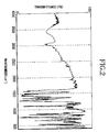
- Fig. 2 is shows an infrared absorption spectrum of Compound (2).
- Fig. 3 is shows an infrared absorption spectrum of Compound (9).
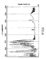
- Fig. 4 is shows an infrared absorption spectrum of Compound (12).
- Fig. 5 is shows an infrared absorption spectrum of Compound (16).
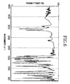
- Fig. 6 is shows an infrared absorption spectrum of Compound (17).
- the ligand represented by each of Q 1 to Q 4 includes quinoline moieties such as 8-hydroxyquinoline and 2-methyl-8-hydroxyquinoline, while the ligand shall not be limited to these.
- a 1 and A 2 are substituted or unsubstituted six-membered aryl rings which are mutually fused to form a fused ring moiety.
- the fused ring moiety has the structure of an aryl ring or a heterocyclic ring.
- the metal complex in the present invention has a stronger quality as an n-type semiconductor and the high capability of injecting electrons. Further, since the formation energy at a complex formation time is low, the bonding strength of the metal and the ligands in the metal complex is high, and the fluorescence quantum efficiency as a light-emitting material is high.
- substituent on the fused ring of A 1 and A 2 forming the ligand of the general formula (2) include halogen atoms such as chlorine, bromine, iodine and fluorine; substituted or unsubstituted alkyl groups such as methyl, ethyl, propyl, butyl, sec-butyl, tert-butyl pentyl, hexyl, heptyl, octyl, stearyl and trichloromethyl; substituted or unsubstituted aryl groups such as phenyl, naphthyl, 3-methylphenyl, 3-methoxyphenyl, 3-fluorophenyl, 3-trichloromethylphenyl, 3-trifluoromethylphenyl and 3-nitrophenyl; substituted or unsubstituted alkoxy groups such as methoxy, n-butoxy, tert-butoxy, trichloromethoxy, trifluoroethoxy
- the gallium complex of the present invention can give an organic EL device having high performances.
- the gallium complex of the present invention is used as a light-emitting material, there are obtained organic EL devices which exhibit high light emission efficiency in a broad light emission range of from blue to green.
- the gallium complex of the present invention is used as a layer such as an electron-injecting layer or an electron-injection type light-emitting layer, which is in contact directly to a cathode, the device has the high capability of transporting electrons and the high capability of accepting electrons from a cathode, and the gallium complex of the present invention is therefore a remarkably advantageous material for an organic EL device.
- most of the gallium complexes of the present invention have a melting point of at least 300°C, and this point is advantageous for manufacturing an organic EL device having a high light emission brightness and a long life.
- the ligang L forming the gallium complex of the general formula (1) is a halogen atom, a substituted or unsubstituted alkyl group, a substituted or unsubstituted cycloalkyl group, a substituted or unsubstituted aryl group, a substituted or unsubstituted heterocyclic ring group,-OR 1 in which R 1 is a hydrogen atom, a substituted or unsubstituted alkyl group, a substituted or unsubstituted cycloalkyl group, a substituted or unsubstituted aryl group or a substituted or unsubstituted heterocyclic ring group, or -O-Ga-Q 3 (Q 4 ) in which Q 3 and Q 4 have the same meanings as those of Q 1 and Q 2 .
- ligand L or the substituents include those described concerning the rings A 1 and A 2 .
- the ligand L is preferably -OR 1 .
- R 1 is a hydrogen atom, a substituted or unsubstituted alkyl group, a substituted or unsubstituted cycloalkyl group, a substituted or unsubstituted aryl group or a substituted or unsubstituted heterocyclic ring group.
- Q 1 or Q 2 in the general formula (1) is preferably a compound of the following general formula (3), wherein each of R 2 to R 7 is independently a hydrogen atom, a halogen atom, cyano, nitro, a substituted or unsubstituted alkyl group, a substituted or unsubstituted cycloalkyl group, a substituted or unsubstituted aryl group or a substituted or unsubstituted heterocyclic ring group.
- substituents include those described concerning the rings A 1 and A 2 .
- Q 1 or Q 2 is particularly preferably a compound of the following formula (4).
- the gallium complex of the general formula (1) is synthesized, for example, from gallium as a metal or a gallium compound and compound(s) having ligand residues of Q 1 and Q 2 or L.
- the gallium compound includes alkyl gallium, gallium halide, gallium acetate, gallium nitrate, gallium arsenide, gallium nitride, gallium phosphide, gallium sulfide, gallium selenide, gallium telluride, gallium hydroxide, gallium oxide, gallium alkoxides such as trimethoxygallium, triethoxygallium and triisopropxyallium, and diethylgallium chloride.
- gallium alkoxides are preferred although the gallium compound shall not be limited thereto.
- the ligand residue represented by Q 1 or Q 2 includes quinoline residues such as 8-hydroxyquinoline and 2-methyl-8-hydroxyquinoline.
- the solvent used in the synthesis is selected from methanol, ethanol, isopropanol, ethyl acetate, acetonitrile, 1,4-dioxane, tetrahydrofuran, benzene, toluene, xylene, n-hexane, dimethylformamide, quinoline, sulfolane or water.
- the reaction temperature is determined depending upon the rate of the ligand forming the gallium complex.
- the temperature for the synthesis is preferably between 0°C and 250°C, more preferably 20°C and 80°C.
- the synthesis is carried out for 10 minutes to 24 hours.
- the synthesis conditions shall not be limited to the above-specified, since the synthesis conditions are determined depending upon the gallium compound, the ligand, the solvent and a catalyst used for the synthesis.
- the gallium complex of the general formula (1) is obtained by reacting gallium or the above gallium compound with a ligand residue (ligand compound) having a great steric hindrance as a compound for forming ligand residues represented by Q 1 and Q 2 , to bond two ligand residues per gallium atom.
- the ligand L optionally bonds to a residue and constitutes the gallium complex of the present invention.
- Gallium strongly bonds to an alkyl group, an oxygen atom and a halogen atom and can form a stable gallium complex.
- gallium can form a stable gallium complex with such a 8-hydroxyquinoline having an alkyl group on the 2-position. Gallium is therefore advantageous in this point.
- Table 1 specifically shows typical examples (Compounds (1) to (28)) of the compound of the general formula (1), although the compound of the general formula (1) shall not be limited to these.
- the above gallium complex can be adjusted to one having a necessary purity by cleaning it with water and/or an organic solvent, recrystallization from a proper solvent, a sublimation purification method or a combination of these.
- the organic EL device is a device manufactured by forming one or more organic thin layers between an anode and a cathode.
- a light-emitting layer is formed between an anode and a cathode.
- the light-emitting layer contains a light-emitting material, and the light-emitting layer may further contain a hole-injecting material for transporting holes injected from the anode to the light-emitting material or an electron-injecting material for transporting electrons injected from the cathode to the light-emitting material.
- the organic EL device of a multi-layer type has a layer structure such as anode/hole-injecting layer/light-emitting layer/cathode, anode/light-emitting layer/electron-injecting layer/cathode, or anode/hole-injecting layer/light-emitting layer/electron-injecting layer/cathode.
- the compound of the general formula (1) can transport holes or electrons, while it can be used in the electron-injecting layer since it is superior in the capability of transporting electrons. Further, the compound of the general formula (1) can be used as a light-emitting layer since EL devices having light-emitting layers containing compounds of the general formula (1) emit fluorescence of intense blue to intense green. Therefore, the compound of the general formula (1) can give an organic EL device having high light emission characteristics.
- a multi-layer structure of the organic EL device can serve to prevent quenching from degrading the brightness and the device life.
- at least two members of a light-emitting material, a dopant, and a hole-injecting material and an electron-injecting material for carrier transportation may be used in combination.
- each of the hole-injecting layer, the light-emitting layer and the electron-injecting layer may have the structure of at least two layers, and a device structure is selected such that holes or electrons can be effectively injected from the anode or the cathode and effectively transported through a layer.
- the light-emitting material or the dopant which can be used together is selected from known materials such as naphthalene, anthracene, phenanthrene, pyrene, tetracene, coronene, chrysene, fluorescein, perylene, phthaloperylene, naphthaloperylene, perinone, naphthaloperinone, diphenylbutadiene, tetraphenylbutadiene, coumarine, oxadiazole, aldazine, bisbenzoxazoline, bisstyryl, diamine, pyrazine, cyclopentadiene, quinoline metal complex, aminoquinoline metal complex, benzoquinoline metal complex, imine, diphenylethylene, vinyl anthracene, diaminocarbazole, pyrane, thiopyrane, polymethine, mer
- the above metal complex compound includes lithium (8-hydroxyquinolinate), zinc bis(8-hydroxyquinolinate), manganese bis(8-hydroxyquinolinate), copper bis(8-hydroxyquinolinate), aluminum tris(8-hydroxyquinolinate), gallium tris(8-hydroxyquinolinate), beryllium bis(10-hydroxybenzo[h]quinolinate), zinc bis(10-hydroxybenzo[h]quinolinate), magnesium bis(10-hydroxybenzo[h]quinolinate), aluminum tris(10-hydroxybenzo[h]quinolinate, chlorogallium bis(2-methyl-8-quinolinate), gallium bis(2-methyl-8-quinolinate)(o-cresolate), aluminum bis(2-methyl-8-quinolinate)(1-phenolate), gallium bis(2-methyl-8-quinolinate)(2-phenolate), aluminum bis(2-methyl-8-quinolinate)(1-naphtholate), gallium bis(2-methyl-8-quinolinate)(1-naphtholate), zinc bis(2-[2-benzox
- the above bisstyryl compound includes divalent residues which may have a substrate as a binding group such as phenylene residue, naphthylene residue, biphenylene residue, anthranylene residue, pyrenylene residue, thiophenylene residue, triphenylamine residue and N-ethylcarbazole residue.
- bisstyryl compound examples include diphenylamino-1,4-bisstyrylbenzene, ditrylamino-1,4-bisstyrylbenzene, diphenylamino-4,4'-bisstyrylbiphenyl, 3-(N-ethylcarbazole)-4,4'-bisstyrylbiphenyl, and bis(4,4'-[2,2-diphenylvinyl])biphenyl.
- the above compounds may be used alone or in combination.
- the conjugated polymer is a polymer having 2 to 10,000 recurring units, obtained by polymerizing only an arylene which may contain a nitrogen, oxygen or sulfur atom, or by polymerizing the arylene and a conjugated compound such as a vinyl compound.
- Specific examples of the cojugated polymer include poly(p-phenylene), poly(o-thiphene), poly(p-phenylenevinylene), poly(2,5-dipentyl-p-phenylenevinylene), poly(2,5-dipentyl-m-phenylenevinylene), poly(2,5-dioctyl-p-phenylenevinylene), poly(2,5-dihexyloxy-p-phenylenevinylene), poly(2,5-dihexyloxy-m-phenylenevinylene), poly(2,5-dihexylthio-p-phenylenevinylene), poly(2,5-didecyloxy-p-phenylenevinylene), poly(2-
- the above arylamine derivative is a compound obtained by substituting a substituted diamino group in an arylene which may contain a nitrogen, oxygen or sulfur atom.
- Specific examples of the arylamine derivative include N,N,N',N'-(4-methylphenyl)-1,4'-phenyl-4,4'-diamine, N,N,N',N'-(4-methylphenyl)-1,3'-phenyl-4,4'-diamine, N,N'-diphenyl-N,N'-(3-methylphenyl)-1,1'-biphenyl-4,4'-diamine, N,N'-(4-methylphenyl)-N,N'-(4-n-butylphenyl)-phenathrene-9,10-dimaine, N,N'-diphenyl-N,N'-dinaphthyl-1,1'-biphenyl-4,4'-diamine, N,N
- the hole-injecting material is a material which is capable of transporting holes, receiving holes from an anode, injecting holes into a light-emitting layer or light-emitting material, preventing excitons generated in a light-emitting layer from moving an electron-injecting layer or electron-injecting material and forming a thin film.
- the hole-injecting material include a phthalocyanine derivative, a naphthalocyanine derivative, a porphyrin derivative, oxadiazole, triazole, imidazole, imidazolone, imidazolthione, pyrazoline, pyrazolone, tetrahydroimidazole, hydrazone, acylhydrazone, polyarylalkane, stilbene, butadiene, benzidine type triphenylamine, styrylamine type triphenylamine, diamine type triphenylamine, derivatives of these, and polymer materials such as polyvinylcarbazole, polysilane and an electrically conductive polymer.
- the electron-injecting material that can be used together is a material which is capable of transporting electrons, receiving electrons from a cathode, injecting electrons into a light-emitting layer or light-emitting material, preventing excitons generated in the light-emitting layer from moving into a hole-injecting layer or hole-injecting material and forming a thin film.
- examples of the electron-injecting material include fluorenone, anthraquinodimethane, diphenoquinone, thiopyran dioxide, oxadiazole, thiadiazole, triazole, tetrazole, imidazole, perylenetetracarboxylic acid, fluorenylidenemethane, anthraquinodimethane, anthrone, a metal complex and derivatives of these.
- the hole-injecting material may be sensitivity-increased by incorporating an electron-accepting material, and the electron-injecting material may be sensitivity-increased by incorporating an electron-donating material. Further, the hole-injecting material can be selected from the above hole-injecting materials.
- the gallium complex of the present invention can be used as a light-emitting material in a light-emitting layer.
- the light-emitting layer may contain at least one selected from a light-emitting material, a dopant, a hole-injecting material or an electron-injecting material in combination with the gallium complex of the present invention.
- the gallium complex of the present invention can be used in/as an electron-injecting layer between a light-emitting layer and a cathode since it is highly capable of receiving electrons from a cathode of a metal and transporting the electrons.
- the electrically conductive material used for the anode of the organic EL device is suitably selected from those materials having a work function of greater than 4 eV.
- This electrically conductive material includes carbon, aluminum, vanadium, iron, cobalt, nickel, tungsten, silver, gold, platinum, palladium, alloys of these, metal oxides such as tin oxide and indium oxide used for ITO substrates or NESA substrates, and organic electrically conductive resins such as polythiophene and polypyrrole.
- the electrically conductive material used for the cathode is suitably selected from those having a work function of smaller than 4 eV.
- This electrically conductive material includes magnesium, calcium, tin, lead, titanium, yttrium, lithium, ruthenium, manganese, aluminum and alloys of these, while it shall not be limited to these.
- Typical examples of the alloys include magnesium/silver, magnesium/indium and lithium/aluminum, while the alloys shall not be limited to these.
- the metal ratio of the alloy is properly controlled by controlling the temperature of a deposition source, atmosphere and the degree of vacuum.
- Each of the anode and the cathode may have a structure of at least two layers as required.
- At least one of the electrodes is desirably transparent in the light emission wavelength region of the device.
- the substrate is desirably transparent.
- the transparent electrode is produced from the above electrically conductive material by a deposition method or a sputtering method such that a predetermined transparency is secured.
- the electrode which forms a light emission surface preferably has a light transmittance of at least 10 %.
- the substrate is not specially limited if it has adequate mechanical and thermal strength and is transparent. For example, it is selected from glass substrates and substrates of transparent resins such as a polyethylene substrate, a polyethylene terephthalate substrate, a polyether sulfone substrate and a polypropylene substrate.
- Each of the layers forming the organic EL device of the present invention can be formed by any one of dry film forming methods such as a vacuum deposition method, a sputtering method, a plasma method and an ion plating method and wet film forming methods such as a spin coating method, a dipping method and a flow coating method.
- the thickness of each layer is not specially limited, while each layer is required to have a proper thickness. When the layer thickness is too large, inefficiently, a high voltage is required to achieve predetermined emission of light. When the layer thickness is too small, the layer is liable to have a pinhole, etc., so that sufficient light emission brightness is hard to obtain when an electric field is applied.
- the thickness of each layer is preferably in the range of from 5 nm to 10 ⁇ m, more preferably 10 nm to 0.2 ⁇ m.
- a material for forming an intended layer is dissolved or dispersed in a proper solvent, and a thin film is formed from the solution or dispersion.
- the solvent is selected from ethanol, chloroform, tetrahydrofuran and dioxane, while the solvent shall not be limited to these.
- the above solution or dispersion for forming the layer may contain a proper resin and a proper additive.
- the resin suitable for use in the present invention includes insulating resins such as polystyrene, polycarbonate, polyarylate, polyester, polyamide, polyurethane, polysulfone, polymethyl methacrylate, polymethyl acrylate and cellulose, copolymers of these, photoconductive resins such as poly-N-vinylcarbozole and polysilane, and electrically conductive resins such as polythiophene and polypyrrole.
- the above additive includes an antioxidant, an ultraviolet absorbent and a plasticizer.
- a protective layer may be formed on the surface of the device, or the device as a whole may be sealed with a silicone oil, or the like.
- the organic EL device has a light-emitting layer or an electron-injecting layer which contains the gallium complex of the general formula (1), and the organic EL device is therefore improved in properties such as light emission efficiency, maximum light emission brightness, etc. Further, the organic EL device is highly stable against heat and electric current, and further it exhibits practically usable light emission brightness at a low voltage, so that the deterioration of the device, a vital problem of prior art devices, can be remarkably decreased.
- the organic EL device of the present invention can be applied to a flat panel display of a wall-mountable TV set, a light source for a copying machine or a printer, a light source for a liquid crystal display or a counter, a display board and a sign lamp as aa flat light-emitter.
- the organic EL device of the present invention is therefore greatly industrially valuable.
- Examples used glass substrates with ITO electrode having a surface resistance of 10 ( ⁇ / ⁇ ) for producing organic EL devices.
- the gallium complex of the present invention was used as a light-emitting material in a light-emitting layer.
- Compound (29) having the following chemical structure was vacuum-deposited on a cleaned glass plate with an ITO electrode to form a hole-injecting layer having a thickness of 50 mm. Then, Compound (1) as a light-emitting material was vacuum-deposited thereon to form a light-emitting layer having a thickness of 50 nm. An electrode having a thickness of 150 nm was formed thereon from a magnesium/silver alloy having a magnesium/silver mixing ratio of 10/1, to obtain an organic EL device. The hole-injecting layer, the light-emitting layer and the cathode were formed under a vacuum of 10 -6 Torr at a substrate temperature of room temperature.
- the above organic EL device was measured for a light emission brightness with an LS-100 (supplied by Minolta Camera Co., Ltd.).
- Organic EL devices obtained in Examples hereinafter were also measured for brightness and determined for light emission efficiency in the above manner.
- Organic EL devices were prepared in the same manner as in Example 1 except that the light-emitting material was replaced with compounds shown in Table 2. The organic EL devices were measured for light emission brightnesses at a direct current voltage of 12 V and light emission efficiencies. Table 2 shows the results. Table 2 Example Compound Brightness (cd/m 2 ) Light emission efficiency (lm/W) 2 (2) 6,500 0.53 3 (3) 6,000 0.51 4 (6) 6,000 0.50 5 (4) 6,800 0.55 6 (5) 7,100 0.61 7 (7) 6,900 0.57 8 (9) 7,000 0.57 9 (18) 7,000 0.53 10 (20) 6,800 0.55 11 (19) 6,800 0.55 12 (21) 6,300 0.52 13 (22) 6,500 0.54 14 (25) 6,600 0.55 15 (26) 7,200 0.63 16 (27) 6,000 0.50
- Compound (1) and poly-N-vinylcarbazole in a Compound (1)/poly-N-vinylcarbazole weight ratio of 3/5 were dissolved and dispersed in chloroform, and the solution was spin-coated on a cleaned glass substrate with an ITO electrode to form a light-emitting layer having a thickness of 100 m. Then, an electrode having a thickness of 150 nm was formed thereon from a magnesium/silver alloy having a magnesium/silver mixing ratio of 10/1, to obtain an organic EL device.
- the cathode was formed by deposition under a vacuum of 10 -6 Torr at a substrate temperature of room temperature.
- the organic EL device showed a blue light emission of 1,000 (cd/m 2 ) at a direct current voltage of 12 V and a light emission efficiency of 0.23 (lm/W).
- Compound (29) was dissolved and dispersed in chloroform, and the solution was spin-coated on a cleaned glass substrate with an ITO electrode to form a hole-injecting layer having a thickness of 30 nm. Then, Compound (26) was vapor-deposited thereon to form a light-emitting layer having a thickness of 50 nm. Further, 2-(4-tert-butylphenyl)-5-(biphenyl)-1,3,4-oXadiazole was vacuum-deposited thereon to form an electron-injecting layer having a thickness of 20 nm.
- an electrode having a thickness of 150 nm was formed thereon from a magnesium/silver alloy having a magnesium/silver mixing ratio of 10/1, to obtain an organic EL device.
- the light-emitting layer, the electron-injecting layer and the cathode were formed by deposition under a vacuum of 10 -6 Torr at a substrate temperature of room temperature.
- the organic EL device showed a bluish green light emission of 6,500 (cd/m 2 ) at a direct current voltage of 12 V and a light emission efficiency of 0.65 (lm/W).
- Compound (29) was vacuum-deposited on a cleaned glass substrate with an ITO electrode to form a hole-injecting layer having a thickness of 30 nm. Then, Compound 7 was vapor-deposited thereon to form a light-emitting layer having a thickness of 30 nm. Further, Compound (25) was vacuum-deposited thereon to form an electron-injecting layer having a thickness of 20 nm. Then, an electrode having a thickness of 150 nm was formed thereon from a magnesium/silver alloy having a magnesium/silver mixing ratio of 10/1, to obtain an organic EL device.
- the hole-injecting layer, the light-emitting layer, the electron-injecting layer and the cathode were formed by deposition under a vacuum of 10 -6 Torr at a substrate temperature of room temperature.
- the organic EL device showed a blue light emission of 6,300 (cd/m 2 ) at a direct current voltage of 12 V and a light emission efficiency of 0.68 (lm/W).
- Compound (31) having the following chemical structure was vacuum-deposited on a cleaned glass substrate with an ITO electrode to form a hole-injecting layer having a thickness of 30 mm. Then, Compound (7) was vapor-deposited thereon to form a light-emitting layer having a thickness of 40 nm. Further, Compound (17) was vacuum-deposited thereon to form an electron-injecting layer having a thickness of 20 nm. Then, an electrode having a thickness of 150 nm was formed thereon from a magnesium/silver alloy having a magnesium/silver mixing ratio of 10/1, to obtain an organic EL device.
- the hole-injecting layer, the light-emitting layer, the electron-injecting layer and the cathode were formed by deposition under a vacuum of 10 -6 Torr at a substrate temperature of room temperature.
- the organic EL device showed a blue light emission of 16,000 (cd/m 2 ) at a direct current voltage of 8 V and a light emission efficiency of 2.04 (lm/W).
- the gallium complex of the present invention was used as an electron-injecting material in an electron-injecting layer.
- Compound (31) was vacuum-deposited on a cleaned glass substrate with an ITO electrode to form a hole-injecting layer having a thickness of 30 nm. Then, Compound (32) having the following chemical structure was vapor-deposited thereon to form a light-emitting layer having a thickness of 40 nm. Further, Compound (9) was vacuum-deposited thereon to form an electron-injecting layer having a thickness of 20 nm. Then, an electrode having a thickness of 150 nm was formed thereon from an aluminum/lithium alloy having an aluminum/lithium mixing ratio of 100/3, to obtain an organic EL device.
- the hole-injecting layer, the light-emitting layer, the electron-injecting layer and the cathode were formed by deposition under a vacuum of 10 -6 Torr at a substrate temperature of room temperature.
- the organic EL device showed a yellowish green light emission of 13,500 (cd/m 2 ) at a direct current voltage of 8 V.
- Compound (31) was vacuum-deposited on a cleaned glass substrate with an ITO electrode to form a hole-injecting layer having a thickness of 30 nm. Then, Compound (33) having the following chemical structure was vapor-deposited thereon to form a light-emitting layer having a thickness of 40 nm. Further, Compound (9) was vacuum-deposited thereon to form an electron-injecting layer having a thickness of 20 nm. Then, an electrode having a thickness of 150 nm was formed thereon from an aluminum/lithium alloy having an aluminum/lithium mixing ratio of 100/3, to obtain an organic EL device.
- the hole-injecting layer, the light-emitting layer, the electron-injecting layer and the cathode were formed by deposition under a vacuum of 10 -6 Torr at a substrate temperature of room temperature.
- the organic EL device showed a blue light emission of 12,000 (cd/m 2 ) at a direct current voltage of 8 V.
- Compound (31) was vacuum-deposited on a cleaned glass substrate with an ITO electrode to form a hole-injecting layer having a thickness of 30 nm. Then, a solution of poly(2,5-hexylthio-p-phenylenevinylene) having a number average molecular weight of 25,000 in chloroform was spin-coated on the hole-injecting layer to form a light-emitting layer having a thickness of 40 nm. Further, Compound (9) was vacuum-deposited thereon to form an electron-injecting layer having a thickness of 20 nm.
- an electrode having a thickness of 150 nm was formed thereon from a magnesium/silver alloy having a magnesium/silver mixing ratio of 10/1, to obtain an organic EL device.
- the hole-injecting layer, the electron-injecting layer and the cathode were formed by deposition under a vacuum of 10 -6 Torr at a substrate temperature of room temperature.
- the organic EL device showed a greenish yellow light emission of 10,500 (cd/m 2 ) at a direct current voltage of 8 V.
- Compound (31) was vacuum-deposited on a cleaned glass substrate with an ITO electrode to form a hole-injecting layer having a thickness of 30 nm. Then, Compound (30) was vapor-deposited thereon to form a light-emitting layer having a thickness of 40 nm. Further, Compound (7) was vacuum-deposited thereon to form an electron-injecting layer having a thickness of 20 nm. Then, an electrode having a thickness of 150 nm was formed thereon from an aluminum/lithium alloy having an aluminum/lithium mixing ratio of 100/3, to obtain an organic EL device.
- the hole-injecting layer, the light-emitting layer, the electron-injecting layer and the cathode were formed by deposition under a vacuum of 10 -6 Torr at a substrate temperature of room temperature.
- the organic EL device showed a bluish green light emission of 15,000 (cd/m 2 ) at a direct current voltage of 8 V and a light emission efficiency of 2.35 (lm/W).
- An organic EL device was obtained in the same manner as in Example 21 except that Compound (7) for a light-emitting material was replaced with Compound (34) having the following chemical structure.
- the organic EL device was measured for a light emission brightness.
- the organic EL device showed a yellowish green light emission of 11,000 (cd/m 2 ) at a direct current voltage of 8 V and a light emission efficiency of 0.81 (lm/W). It was found that the light emission was made from Compound (34).
- Organic EL devices were obtained in the same manner as in Example 25 except that Compound (7) for an electron-injecting layer was replaced with compounds shown in Table 3. The organic EL devices were measured for light emission brightness at a direct current voltage of 8 V.
- the organic EL devices obtained in the above Examples having the structure of at least 2 layers, showed a light emission color of from blue to bluish green, a light emission brightness of at least 5,000 cd/m 2 and high light emission efficiency. Further, when the organic EL devices obtained in the above Examples were allowed to continuously emit light at 3 mA/cm 2 , all the organic EL devices emitted light having a brightness of at least 1/2 of the initial brightness for more than 10,000 hours. While the organic EL device obtained in Example 25 had a stable light emission brightness for more than 10,000 hours and showed almost no dark spots, while the organic EL devices obtained under the same conditions in Comparative Examples 2 and 3 showed light emission brightnesses which decreased to 1/2 or less of the initial brightness within 500 hours.
- the organic EL devices obtained in Comparative Examples 2 and 3 showed many dark spots, and with the passage of time in measurement, the number of dark spots increased, and the sizes thereof increased.
- the reason therefor is assumed to be as follows. Compounds used in place of the compound of the present invention was poor in adhesion to the light-emitting layer and to the cathode and in formability, and the light-emitting layer and the cathode were greatly different in work function.
- the above results show that the use of the gallium complex of the present invention in the light-emitting layer or in a layer between the light-emitting layer and the cathode gives an organic EL device having a high light emission efficiency and an increased device life.
- the organic EL device according to the present invention accomplishes improvements in light emission efficiency and brightness, and achieves an increased device life. There is therefore no limitation to be imposed on the light-emitting material, dopant, hole-injecting material, electron-injecting material, sensitizer, resin and electrode material which are used in combination of the gallium complex of the present invention, nor is the method of producing the device limited.
- An organic EL device having a light-emitting layer formed of the gallium complex of the present invention or a layer formed of the gallium complex of the present invention between a light-emitting layer and a cathode exhibits a high light emission efficiency and an increased device life as compared with conventional organic EL devices.
- the gallium complex of the present invention is used to form at least one layer of an organic EL device, the organic EL device exhibits a high light emission brightness, a high light emission efficiency and a long device life.
- an alkyl group or moiety is typically a C 1 -C 18 alkyl group or moiety, preferably a C 1 -C 8 alkyl group or moiety, more preferably a C 1 -C 6 alkyl group or moiety.
- Substituted alkyl groups include haloalkyl groups, for example chloro- or fluoro-alkyl groups which may comprise one or more halogen substituents.
- An aryl group or moiety is typically a C 5 -C 16 aryl group or moiety, preferably a C 5 -C 14 aryl group or moiety, more preferably a C 5 -C 10 aryl group or moiety.
- An aryl group or moiety may be substituted by one or more substituents such as a halogen, alkyl, alkoxy or nitro substituent.
- a mono or di substituted amino group is typically substituted by one or two alkyl, aryl or acyl moieties.
- An acyl group or moiety is typically a C 2 -C 6 , preferably a C 2 -C 4 acyl group or moiety.
- a carbamoyl group is typically substituted by one or two alkyl or aryl moieties.
- a cycloalkyl group or moiety is typically a C 3 -C 6 cycloalkyl group or moiety.
- a heterocyclic group is typically a 3 to 14 membered heterocyclic group, preferably a 4 to 10 membered heterocyclic group containing one, two or three heteroatoms selected from N, O and S.
- R 1 as defined above, include those described concerning the rings A 1 and A 2 .
Abstract

wherein Q1 and Q2 are the same or different and each is a ligand of the general formula (2),

wherein A1 and A2 are substituted or unsubstituted six-membered aryl rings which are mutually fused to form a fused ring moiety, and
L is a halogen atom, a substituted or unsubstituted alkyl group, a substituted or unsubstituted cycloalkyl group, a substituted or unsubstituted aryl group, a substituted or unsubstituted heterocyclic group,
-OR1 in which R1 is a hydrogen atom, a substituted or unsubstituted alkyl group, a substituted or unsubstituted cycloalkyl group, a substituted or unsubstituted aryl group or a substituted or unsubstituted heterocyclic group, or -O-Ga-Q3(Q4) wherein Q3 and Q4 are the same or different and have the same meanings as Q1 and Q2.
Description
- The present invention relates to an organoelectroluminescence ("EL" hereinafter) device used as a flat light source or display, more specifically to a light-emitting device having a high brightness.
- An EL device using an organic substance is greatly expected to be usable as a solid light-emitting inexpensive large-screen, full-color display device, and the development thereof is being made in many ways. Generally, an EL device is composed of a light-emitting layer and a pair of mutually opposite electrodes sandwiching the light-emitting layer. Light emission is the following phenomenon. When an electric field is applied between these two electrodes, the cathode injects electrons into the light-emitting layer, and the anode injects holes into the light-emitting layer. When the electrons recombine with the holes in the light-emitting layer, their energy level shifts to a valence bond band to release energy as fluorescent light.
- As compared with inorganic EL devices, conventional organic EL devices require high voltage, and their light emission brightness and light emission efficiency are low. Further, conventional organic EL devices deteriorate in properties to a great extent, and no organic EL device has been put to practical use.
- There has been recently proposed an organic EL device which is produced by laminating a thin film containing an organic compound having a fluorescent quantum effect of emitting light at a low voltage as low as less than 10 V, and it attracts attention (Appl. Phy. Lett., Vol. 51, page 913, 1987). The above organic EL device has a fluorescent layer containing a metal chelate complex and a hole-injecting layer containing an amine-based compound, and emits green light having a high brightness. The above organic EL device achieves nearly practically usable performance, since it accomplishes a brightness of 1,000 cd/m2 and a maximum light emission efficiency of 1.5 lm/W at a direct current voltage of 6 or 7V.
- However, conventional organic EL devices including the above organic EL device are not yet satisfactory in brightness although these organic EL devices are improved in brightness to some extent. The serious problem is that they are insufficient in light emission stability in their continuous operation for a long period of time. Fewer materials which emit blue light perform adequate brightness or light emission efficiency, and it has been desired to develop light-emitting materials for the device.
- It is an object of the present invention to provide a material which can give an organic EL device excellent in stability in the repetitive operation, and an organic EL device for which the material is adapted.
- It is another object of the present invention to provide a material which can give an organic EL device which has a high light emission brightness and is excellent in stability in the repetitive operation, and an organic EL device for which the material is adapted.
- According to the present invention, there is provided an organic EL device material (gallium complex) of the general formula (1)


- According to the present invention, there is also provided an organic EL device comprising a light-emitting layer or a plurality of thin organic compound layers including the light-emitting layer, the light-emitting layer or a plurality of the thin organic compound layers being sandwiched between an anode and a cathode, wherein the light-emitting layer or at least one of a plurality of the thin organic compound layers contains the above organic EL device material (gallium complex).
- Fig. 1 is shows an infrared absorption spectrum of Compound (1).
- Fig. 2 is shows an infrared absorption spectrum of Compound (2).
- Fig. 3 is shows an infrared absorption spectrum of Compound (9).
- Fig. 4 is shows an infrared absorption spectrum of Compound (12).
- Fig. 5 is shows an infrared absorption spectrum of Compound (16).
- Fig. 6 is shows an infrared absorption spectrum of Compound (17).
- In the general formula (1), the ligand represented by each of Q1 to Q4 includes quinoline moieties such as 8-hydroxyquinoline and 2-methyl-8-hydroxyquinoline, while the ligand shall not be limited to these.
- In the general formula (2), A1 and A2 are substituted or unsubstituted six-membered aryl rings which are mutually fused to form a fused ring moiety. The fused ring moiety has the structure of an aryl ring or a heterocyclic ring. The metal complex in the present invention has a stronger quality as an n-type semiconductor and the high capability of injecting electrons. Further, since the formation energy at a complex formation time is low, the bonding strength of the metal and the ligands in the metal complex is high, and the fluorescence quantum efficiency as a light-emitting material is high.
- Specific examples of the substituent on the fused ring of A1 and A2 forming the ligand of the general formula (2) include halogen atoms such as chlorine, bromine, iodine and fluorine; substituted or unsubstituted alkyl groups such as methyl, ethyl, propyl, butyl, sec-butyl, tert-butyl pentyl, hexyl, heptyl, octyl, stearyl and trichloromethyl; substituted or unsubstituted aryl groups such as phenyl, naphthyl, 3-methylphenyl, 3-methoxyphenyl, 3-fluorophenyl, 3-trichloromethylphenyl, 3-trifluoromethylphenyl and 3-nitrophenyl; substituted or unsubstituted alkoxy groups such as methoxy, n-butoxy, tert-butoxy, trichloromethoxy, trifluoroethoxy, pentafluoropropoxy, 2,2,3,3-tetrafluoropropoxy, 1,1,1,3,3,3-hexafluoro-2-propoxy and 6-(perfluoroethyl)hexyloxy; substituted or unsubstituted aryloxy groups such as phenoxy, p-nitrophenoxy, p-tert-butylphenoxy, 3-fluorophenoxy, pentafluorophenoxy and 3-trifluoromethylphenoxy; substituted or unsubstituted alkylthio groups such as methylthio, ethylthio, tert-butylthio, hexylthio, octylthio and trifluoromethylthio; substituted or unsubstituted arylthio groups such as phenylthio, p-nitrophenylthio, p-tert-butylphenylthio, 3-fluorophenylthio, pentafluorophenylthio and 3-trifluoromethylphenylthio; mono-or di-substituted amino groups such as cyano, nitro, amino, methylamino, dimethylamino, ethylamino, diethylamino, dipropylamino, dibutylamino and diphenylamino; acylamino groups such as bis(acetoxymethyl)amino, bis(acetoxyethyl)amino, bis(acetoxypropyl)amino and bis(acetoxybutyl)amino; carbamoyl groups such as hydroxyl, siloxy, acyl, methylcarbamoyl, dimethylcarbamoyl, ethylcarbamoyl, diethylcarbamoyl, propylcarbamoyl, butylcarbamoyl and phenylcarbamoyl; carboxyl acid group; sulfonic acid group; imido group; cycloalkyl groups such as cyclopentyl and cyclohexyl; aryl groups such as phenyl, naphthyl, biphenyl, anthranyl, phenahtryl, fluorenyl and pyrenyl; and heterocyclic groups such as pyrizinyl, pyrazinyl, pyrimidinyl, pyridazinyl, triazinyl, indolinyl, quinolinyl, acridinyl, pyrolidinyl, dioxanyl, piperidinyl, morpholinyl, piperazinyl, triathinyl, carbazolyl, furanyl, thiophenyl, oxazolyl, oxadiazolyl, penzoxazolyl, thiazolyl, thiadiazolyl, benzothiazoly, triazolyl, imidazolyl, benzoimidazolyl and puranyl. Further, any two members of the above substituents may bond together to form a six-membered ary ring or heterocyclic ring.
- The gallium complex of the present invention can give an organic EL device having high performances. When the gallium complex of the present invention is used as a light-emitting material, there are obtained organic EL devices which exhibit high light emission efficiency in a broad light emission range of from blue to green. When the gallium complex of the present invention is used as a layer such as an electron-injecting layer or an electron-injection type light-emitting layer, which is in contact directly to a cathode, the device has the high capability of transporting electrons and the high capability of accepting electrons from a cathode, and the gallium complex of the present invention is therefore a remarkably advantageous material for an organic EL device. Further, most of the gallium complexes of the present invention have a melting point of at least 300°C, and this point is advantageous for manufacturing an organic EL device having a high light emission brightness and a long life.
- The ligang L forming the gallium complex of the general formula (1) is a halogen atom, a substituted or unsubstituted alkyl group, a substituted or unsubstituted cycloalkyl group, a substituted or unsubstituted aryl group, a substituted or unsubstituted heterocyclic ring group,-OR1 in which R1 is a hydrogen atom, a substituted or unsubstituted alkyl group, a substituted or unsubstituted cycloalkyl group, a substituted or unsubstituted aryl group or a substituted or unsubstituted heterocyclic ring group, or -O-Ga-Q3(Q4) in which Q3 and Q4 have the same meanings as those of Q1 and Q2.
- Specific examples of the ligand L or the substituents include those described concerning the rings A1 and A2.
- The ligand L is preferably -OR1. R1 is a hydrogen atom, a substituted or unsubstituted alkyl group, a substituted or unsubstituted cycloalkyl group, a substituted or unsubstituted aryl group or a substituted or unsubstituted heterocyclic ring group. Q1 or Q2 in the general formula (1) is preferably a compound of the following general formula (3),


- The gallium complex of the general formula (1), provided by the present invention, is synthesized, for example, from gallium as a metal or a gallium compound and compound(s) having ligand residues of Q1 and Q2 or L. The gallium compound includes alkyl gallium, gallium halide, gallium acetate, gallium nitrate, gallium arsenide, gallium nitride, gallium phosphide, gallium sulfide, gallium selenide, gallium telluride, gallium hydroxide, gallium oxide, gallium alkoxides such as trimethoxygallium, triethoxygallium and triisopropxyallium, and diethylgallium chloride. Part of each of these gallium compounds may be replaced with acetylacetonate. In view of reactivity and safety in the synthesis, gallium alkoxides are preferred although the gallium compound shall not be limited thereto. The ligand residue represented by Q1 or Q2 includes quinoline residues such as 8-hydroxyquinoline and 2-methyl-8-hydroxyquinoline.
- The solvent used in the synthesis is selected from methanol, ethanol, isopropanol, ethyl acetate, acetonitrile, 1,4-dioxane, tetrahydrofuran, benzene, toluene, xylene, n-hexane, dimethylformamide, quinoline, sulfolane or water. The reaction temperature is determined depending upon the rate of the ligand forming the gallium complex. The temperature for the synthesis is preferably between 0°C and 250°C, more preferably 20°C and 80°C. The synthesis is carried out for 10 minutes to 24 hours. However, the synthesis conditions shall not be limited to the above-specified, since the synthesis conditions are determined depending upon the gallium compound, the ligand, the solvent and a catalyst used for the synthesis.
- The gallium complex of the general formula (1) is obtained by reacting gallium or the above gallium compound with a ligand residue (ligand compound) having a great steric hindrance as a compound for forming ligand residues represented by Q1 and Q2, to bond two ligand residues per gallium atom. The ligand L optionally bonds to a residue and constitutes the gallium complex of the present invention. Gallium strongly bonds to an alkyl group, an oxygen atom and a halogen atom and can form a stable gallium complex. Further, it is difficult to form a stable aluminum complex with 8-hydroxyquinoline having an alkyl group on the 2-position such as 2-methyl-8-hydroxyquinoline, while gallium can form a stable gallium complex with such a 8-hydroxyquinoline having an alkyl group on the 2-position. Gallium is therefore advantageous in this point.
- Table 1 specifically shows typical examples (Compounds (1) to (28)) of the compound of the general formula (1), although the compound of the general formula (1) shall not be limited to these.


- The above gallium complex can be adjusted to one having a necessary purity by cleaning it with water and/or an organic solvent, recrystallization from a proper solvent, a sublimation purification method or a combination of these.
- The organic EL device is a device manufactured by forming one or more organic thin layers between an anode and a cathode. In a mono-layer organic EL device, a light-emitting layer is formed between an anode and a cathode. The light-emitting layer contains a light-emitting material, and the light-emitting layer may further contain a hole-injecting material for transporting holes injected from the anode to the light-emitting material or an electron-injecting material for transporting electrons injected from the cathode to the light-emitting material. The organic EL device of a multi-layer type has a layer structure such as anode/hole-injecting layer/light-emitting layer/cathode, anode/light-emitting layer/electron-injecting layer/cathode, or anode/hole-injecting layer/light-emitting layer/electron-injecting layer/cathode. The compound of the general formula (1) can transport holes or electrons, while it can be used in the electron-injecting layer since it is superior in the capability of transporting electrons. Further, the compound of the general formula (1) can be used as a light-emitting layer since EL devices having light-emitting layers containing compounds of the general formula (1) emit fluorescence of intense blue to intense green. Therefore, the compound of the general formula (1) can give an organic EL device having high light emission characteristics.
- A multi-layer structure of the organic EL device can serve to prevent quenching from degrading the brightness and the device life. Further, at least two members of a light-emitting material, a dopant, and a hole-injecting material and an electron-injecting material for carrier transportation may be used in combination. Further, each of the hole-injecting layer, the light-emitting layer and the electron-injecting layer may have the structure of at least two layers, and a device structure is selected such that holes or electrons can be effectively injected from the anode or the cathode and effectively transported through a layer.
- When the gallium complex of the present invention is used as an electron-injecting material, the light-emitting material or the dopant which can be used together is selected from known materials such as naphthalene, anthracene, phenanthrene, pyrene, tetracene, coronene, chrysene, fluorescein, perylene, phthaloperylene, naphthaloperylene, perinone, naphthaloperinone, diphenylbutadiene, tetraphenylbutadiene, coumarine, oxadiazole, aldazine, bisbenzoxazoline, bisstyryl, diamine, pyrazine, cyclopentadiene, quinoline metal complex, aminoquinoline metal complex, benzoquinoline metal complex, imine, diphenylethylene, vinyl anthracene, diaminocarbazole, pyrane, thiopyrane, polymethine, merocyanine, an imidazole-chelated oxynoid compound, quinacridone, rubrene and derivatives of these, although the above materials shall not be limited to these. In particular, a metal complex compound, a bisstyryl compound, a conjugated polymer and an arylamine derivative are suitable as a light-emitting material.
- The above metal complex compound includes lithium (8-hydroxyquinolinate), zinc bis(8-hydroxyquinolinate), manganese bis(8-hydroxyquinolinate), copper bis(8-hydroxyquinolinate), aluminum tris(8-hydroxyquinolinate), gallium tris(8-hydroxyquinolinate), beryllium bis(10-hydroxybenzo[h]quinolinate), zinc bis(10-hydroxybenzo[h]quinolinate), magnesium bis(10-hydroxybenzo[h]quinolinate), aluminum tris(10-hydroxybenzo[h]quinolinate, chlorogallium bis(2-methyl-8-quinolinate), gallium bis(2-methyl-8-quinolinate)(o-cresolate), aluminum bis(2-methyl-8-quinolinate)(1-phenolate), gallium bis(2-methyl-8-quinolinate)(2-phenolate), aluminum bis(2-methyl-8-quinolinate)(1-naphtholate), gallium bis(2-methyl-8-quinolinate)(1-naphtholate), zinc bis(2-[2-benzoxazolinate]phenolate), and zinc bis(2-[2-benzothiazolinate]phenolate. The above compounds may be used alone or in combination.
- The above bisstyryl compound includes divalent residues which may have a substrate as a binding group such as phenylene residue, naphthylene residue, biphenylene residue, anthranylene residue, pyrenylene residue, thiophenylene residue, triphenylamine residue and N-ethylcarbazole residue. Specific examples of the bisstyryl compound include diphenylamino-1,4-bisstyrylbenzene, ditrylamino-1,4-bisstyrylbenzene, diphenylamino-4,4'-bisstyrylbiphenyl, 3-(N-ethylcarbazole)-4,4'-bisstyrylbiphenyl, and bis(4,4'-[2,2-diphenylvinyl])biphenyl. The above compounds may be used alone or in combination.
- The conjugated polymer is a polymer having 2 to 10,000 recurring units, obtained by polymerizing only an arylene which may contain a nitrogen, oxygen or sulfur atom, or by polymerizing the arylene and a conjugated compound such as a vinyl compound. Specific examples of the cojugated polymer include poly(p-phenylene), poly(o-thiphene), poly(p-phenylenevinylene), poly(2,5-dipentyl-p-phenylenevinylene), poly(2,5-dipentyl-m-phenylenevinylene), poly(2,5-dioctyl-p-phenylenevinylene), poly(2,5-dihexyloxy-p-phenylenevinylene), poly(2,5-dihexyloxy-m-phenylenevinylene), poly(2,5-dihexylthio-p-phenylenevinylene), poly(2,5-didecyloxy-p-phenylenevinylene), poly(2-methoxy-5-hexyloxy-p-phenylenevinylene), poly(2,5-thienylenevinylene), poly(3-n-octyl-2,5-thienylenevinylene), poly(1,4-naphthalenevinylene), poly(9,10-anthracenevinylene) and a copolymer obtained from at least two members of these. The above compounds may be used alone or in combination.
- The above arylamine derivative is a compound obtained by substituting a substituted diamino group in an arylene which may contain a nitrogen, oxygen or sulfur atom. Specific examples of the arylamine derivative include N,N,N',N'-(4-methylphenyl)-1,4'-phenyl-4,4'-diamine, N,N,N',N'-(4-methylphenyl)-1,3'-phenyl-4,4'-diamine, N,N'-diphenyl-N,N'-(3-methylphenyl)-1,1'-biphenyl-4,4'-diamine, N,N'-(4-methylphenyl)-N,N'-(4-n-butylphenyl)-phenathrene-9,10-dimaine, N,N'-diphenyl-N,N'-dinaphthyl-1,1'-biphenyl-4,4'-diamine, N,N,N',N'-(4-methylphenyl)-1,4-naphthyl-4,4'-diamine, N,N,N',N'-(4-n-octylphenyl)-9,10-anthranyl-4,4'-dimaine, and N,N,N',N'-[4-(α,α'-dimethylbenzyl)phenyl]-anthranyl-9,10-diamine. The above compounds may be used alone or in combination.
- The hole-injecting material is a material which is capable of transporting holes, receiving holes from an anode, injecting holes into a light-emitting layer or light-emitting material, preventing excitons generated in a light-emitting layer from moving an electron-injecting layer or electron-injecting material and forming a thin film. Although not specially limited, specific examples of the hole-injecting material include a phthalocyanine derivative, a naphthalocyanine derivative, a porphyrin derivative, oxadiazole, triazole, imidazole, imidazolone, imidazolthione, pyrazoline, pyrazolone, tetrahydroimidazole, hydrazone, acylhydrazone, polyarylalkane, stilbene, butadiene, benzidine type triphenylamine, styrylamine type triphenylamine, diamine type triphenylamine, derivatives of these, and polymer materials such as polyvinylcarbazole, polysilane and an electrically conductive polymer.
- When the gallium complex of the present invention is used as a light-emitting material, the electron-injecting material that can be used together is a material which is capable of transporting electrons, receiving electrons from a cathode, injecting electrons into a light-emitting layer or light-emitting material, preventing excitons generated in the light-emitting layer from moving into a hole-injecting layer or hole-injecting material and forming a thin film. Although not specially limited, examples of the electron-injecting material include fluorenone, anthraquinodimethane, diphenoquinone, thiopyran dioxide, oxadiazole, thiadiazole, triazole, tetrazole, imidazole, perylenetetracarboxylic acid, fluorenylidenemethane, anthraquinodimethane, anthrone, a metal complex and derivatives of these. The hole-injecting material may be sensitivity-increased by incorporating an electron-accepting material, and the electron-injecting material may be sensitivity-increased by incorporating an electron-donating material. Further, the hole-injecting material can be selected from the above hole-injecting materials.
- The gallium complex of the present invention can be used as a light-emitting material in a light-emitting layer. The light-emitting layer may contain at least one selected from a light-emitting material, a dopant, a hole-injecting material or an electron-injecting material in combination with the gallium complex of the present invention. Further, the gallium complex of the present invention can be used in/as an electron-injecting layer between a light-emitting layer and a cathode since it is highly capable of receiving electrons from a cathode of a metal and transporting the electrons.
- The electrically conductive material used for the anode of the organic EL device is suitably selected from those materials having a work function of greater than 4 eV. This electrically conductive material includes carbon, aluminum, vanadium, iron, cobalt, nickel, tungsten, silver, gold, platinum, palladium, alloys of these, metal oxides such as tin oxide and indium oxide used for ITO substrates or NESA substrates, and organic electrically conductive resins such as polythiophene and polypyrrole.
- The electrically conductive material used for the cathode is suitably selected from those having a work function of smaller than 4 eV. This electrically conductive material includes magnesium, calcium, tin, lead, titanium, yttrium, lithium, ruthenium, manganese, aluminum and alloys of these, while it shall not be limited to these. Typical examples of the alloys include magnesium/silver, magnesium/indium and lithium/aluminum, while the alloys shall not be limited to these. The metal ratio of the alloy is properly controlled by controlling the temperature of a deposition source, atmosphere and the degree of vacuum. Each of the anode and the cathode may have a structure of at least two layers as required.
- For the effective light emission of the organic EL device, at least one of the electrodes is desirably transparent in the light emission wavelength region of the device. Further, the substrate is desirably transparent. The transparent electrode is produced from the above electrically conductive material by a deposition method or a sputtering method such that a predetermined transparency is secured. The electrode which forms a light emission surface preferably has a light transmittance of at least 10 %. The substrate is not specially limited if it has adequate mechanical and thermal strength and is transparent. For example, it is selected from glass substrates and substrates of transparent resins such as a polyethylene substrate, a polyethylene terephthalate substrate, a polyether sulfone substrate and a polypropylene substrate.
- Each of the layers forming the organic EL device of the present invention can be formed by any one of dry film forming methods such as a vacuum deposition method, a sputtering method, a plasma method and an ion plating method and wet film forming methods such as a spin coating method, a dipping method and a flow coating method. The thickness of each layer is not specially limited, while each layer is required to have a proper thickness. When the layer thickness is too large, inefficiently, a high voltage is required to achieve predetermined emission of light. When the layer thickness is too small, the layer is liable to have a pinhole, etc., so that sufficient light emission brightness is hard to obtain when an electric field is applied. Generally, the thickness of each layer is preferably in the range of from 5 nm to 10 µm, more preferably 10 nm to 0.2 µm.
- In the wet film forming method, a material for forming an intended layer is dissolved or dispersed in a proper solvent, and a thin film is formed from the solution or dispersion. The solvent is selected from ethanol, chloroform, tetrahydrofuran and dioxane, while the solvent shall not be limited to these. For improving the film formability and preventing the occurrence of pinholes, the above solution or dispersion for forming the layer may contain a proper resin and a proper additive. The resin suitable for use in the present invention includes insulating resins such as polystyrene, polycarbonate, polyarylate, polyester, polyamide, polyurethane, polysulfone, polymethyl methacrylate, polymethyl acrylate and cellulose, copolymers of these, photoconductive resins such as poly-N-vinylcarbozole and polysilane, and electrically conductive resins such as polythiophene and polypyrrole. The above additive includes an antioxidant, an ultraviolet absorbent and a plasticizer.
- For improving the organic EL device of the present invention in the stability against temperature, humidity and ambient atmosphere, a protective layer may be formed on the surface of the device, or the device as a whole may be sealed with a silicone oil, or the like.
- In the present invention, the organic EL device has a light-emitting layer or an electron-injecting layer which contains the gallium complex of the general formula (1), and the organic EL device is therefore improved in properties such as light emission efficiency, maximum light emission brightness, etc. Further, the organic EL device is highly stable against heat and electric current, and further it exhibits practically usable light emission brightness at a low voltage, so that the deterioration of the device, a vital problem of prior art devices, can be remarkably decreased.
- The organic EL device of the present invention can be applied to a flat panel display of a wall-mountable TV set, a light source for a copying machine or a printer, a light source for a liquid crystal display or a counter, a display board and a sign lamp as aa flat light-emitter. The organic EL device of the present invention is therefore greatly industrially valuable.
- The present invention will be further explained with reference to Examples hereinafter. Examples used glass substrates with ITO electrode having a surface resistance of 10 (Ω/□) for producing organic EL devices.
- 5.0 Grams of anhydrous gallium trichloride and 100 ml of anhydrous ethanol were placed in a flask and stirred. Further, a solution of 9.0 g of 8-hydroxyquinaldine in 100 ml of anhydrous ethanol was dropwise added. The mixture was stirred at room temperature for 1 hour to precipitate a solid, and the solid was recovered by filtration, washed with anhydrous ethanol and vacuum-dried to give 8.9 g of a yellowish white powder. The yellowish white powder was subjected to elemental analysis and mass analysis and measured for infrared absorption spectrum and NMR spectrum to show that the powder was Compound (1). Fig. 1 shows the infrared absorption spectrum of Compound (1).
- 5.0 Grams of trimethoxygallium and 100 g of anhydrous ethanol were placed in a flask and stirred. Further, a solution of 9.0 g of 8-hydroxyquinaldine in 140 g of anhydrous ethanol was dropwise added, and the mixture was stirred at 60°C for 30 minutes. Further, 2.9 g of phenol was added, and the mixture was stirred at 70dC for 30 minutes. Then, 4.9 g of 8-hydroxyquinaldine was added, and the mixture was stirred at 70°C for 5 hours to precipitate a solid. The solid was recovered by filtration, washed with anhydrous ethanol and vacuum-dried to give 6.3 g of a yellowish white powder. The yellowish white powder was subjected to elemental analysis and mass analysis and measured for infrared absorption spectrum and NMR spectrum to show that the powder was Compound (7). Fig. 2 shows the infrared absorption spectrum of Compound (7).
- 5.0 Grams of trimethoxygallium and 100 g of anhydrous ethanol were placed in a flask and stirred. Further, a solution of 9.0 g of 8-hydroxyquinaldine in 140 g of anhydrous ethanol was dropwise added, and the mixture was stirred at 60°C for 30 minutes. Further, 5.3 g of 4-hydroxybiphenyl was added, and the mixture was stirred at 70°C for 30 minutes. Then, 4.9 g of 8-hydroxyquinaldine was added, and the mixture was stirred at 70°C for 5 hours to precipitate a solid. The solid was recovered by filtration, washed with anhydrous ethanol and vacuum-dried to give 7.2 g of a yellowish white powder. The yellowish white powder was subjected to elemental analysis and mass analysis and measured for infrared absorption spectrum and NMR spectrum to show that the powder was Compound (9). Fig. 3 shows the infrared absorption spectrum of Compound (9).
- 7.2 Grams of triisopropoxygallium and 100 g of anhydrous ethanol were placed in a flask and stirred. Further, a solution of 9.0 g of 8-hydroxyquinaldine in 140 g of anhydrous ethanol was dropwise added, and the mixture was stirred at 60°C for 30 minutes. Further, 5.5 g of 4-cyclohexylphenol was added, and the mixture was stirred at 70°C for 30 minutes. Then, 4.9 g of 8-hydroxyquinaldine was added, and the mixture was stirred at 70°C for 5 hours to precipitate a solid. The solid was recovered by filtration, washed with anhydrous ethanol and vacuum-dried to give 7.4 g of a yellowish white powder. The yellowish white powder was subjected to elemental analysis and mass analysis and measured for infrared absorption spectrum and NMR spectrum to show that the powder was Compound (12). Fig. 4 shows the infrared absorption spectrum of Compound (12).
- 5.0 Grams of trimethoxygallium and 100 g of anhydrous ethanol were placed in a flask and stirred. Further, a solution of 9.0 g of 8-hydroxyquinaldine in 140 g of anhydrous ethanol was dropwise added, and the mixture was stirred at 60°C for 30 minutes. Further, 4.5 g of 1-naphthol was added, and the mixture was stirred at 70°C for 30 minutes. Then, 4.9 g of 8-hydroxyquinaldine was added, and the mixture was stirred at 70°C for 5 hours to precipitate a solid. The solid was recovered by filtration, washed with anhydrous ethanol and vacuum-dried to give 6.5 g of a yellowish white powder. The yellowish white powder was subjected to elemental analysis and mass analysis and measured for infrared absorption spectrum and NMR spectrum to show that the powder was Compound (16). Fig. 5 shows the infrared absorption spectrum of Compound (16).
- 5.0 Grams of trimethoxygallium and 100 g of anhydrous ethanol were placed in a flask and stirred. Further, a solution of 9.0 g of 8-hydroxyquinaldine in 140 g of anhydrous ethanol was dropwise added, and the mixture was stirred at 60°C for 30 minutes. Further, 4.5 g of 2-naphthol was added, and the mixture was stirred at 70°C for 30 minutes. Then, 4.9 g of 8-hydroxyquinaldine was added, and the mixture was stirred at 70°C for 5 hours to precipitate a solid. The solid was recovered by filtration, washed with anhydrous ethanol and vacuum-dried to give 6.6 g of a yellowish white powder. The yellowish white powder was subjected to elemental analysis and mass analysis and measured for infrared absorption spectrum and NMR spectrum to show that the powder was Compound (17). Fig. 7 shows the infrared absorption spectrum of Compound (17).
- 9.0 Grams of 8-hydroxyquinaldine, 11.5 g of gallium-di-isopropoxy-acetaylacetate and 200 ml of toluene were placed in a flask and stirred at room temperature for 20 hours. The resultant solution was distilled at 50°C under vacuum (under reduced pressure) to evaporate the toluene, whereby a compound in the form of a yellow paste was obtained. The so-obtained compound was washed with toluene and vacuum-dried to give 8.7 g of a yellowish white powder. The yellowish white powder was subjected to elemental analysis and mass analysis and measured for infrared absorption spectrum and NMR spectrum to show that the powder was Compound (26).
- In the following Examples, the gallium complex of the present invention was used as a light-emitting material in a light-emitting layer.
- Compound (29) having the following chemical structure was vacuum-deposited on a cleaned glass plate with an ITO electrode to form a hole-injecting layer having a thickness of 50 mm. Then, Compound (1) as a light-emitting material was vacuum-deposited thereon to form a light-emitting layer having a thickness of 50 nm. An electrode having a thickness of 150 nm was formed thereon from a magnesium/silver alloy having a magnesium/silver mixing ratio of 10/1, to obtain an organic EL device. The hole-injecting layer, the light-emitting layer and the cathode were formed under a vacuum of 10-6 Torr at a substrate temperature of room temperature. The organic EL device showed a blue light emission of 6,800 (cd/m2) at a direct current voltage of 12 V, a light emission efficiency of 0.52 (lm/W) and a chromaticity of x = 0.290 and y = 0.430.

- The above organic EL device was measured for a light emission brightness with an LS-100 (supplied by Minolta Camera Co., Ltd.). The light emission efficiency η (lm/W) was determined on the basis of the following equation,

- Organic EL devices obtained in Examples hereinafter were also measured for brightness and determined for light emission efficiency in the above manner.
- Organic EL devices were prepared in the same manner as in Example 1 except that the light-emitting material was replaced with compounds shown in Table 2. The organic EL devices were measured for light emission brightnesses at a direct current voltage of 12 V and light emission efficiencies. Table 2 shows the results.
Table 2 Example Compound Brightness (cd/m2) Light emission efficiency (lm/W) 2 (2) 6,500 0.53 3 (3) 6,000 0.51 4 (6) 6,000 0.50 5 (4) 6,800 0.55 6 (5) 7,100 0.61 7 (7) 6,900 0.57 8 (9) 7,000 0.57 9 (18) 7,000 0.53 10 (20) 6,800 0.55 11 (19) 6,800 0.55 12 (21) 6,300 0.52 13 (22) 6,500 0.54 14 (25) 6,600 0.55 15 (26) 7,200 0.63 16 (27) 6,000 0.50 - Compound (1) and poly-N-vinylcarbazole in a Compound (1)/poly-N-vinylcarbazole weight ratio of 3/5 were dissolved and dispersed in chloroform, and the solution was spin-coated on a cleaned glass substrate with an ITO electrode to form a light-emitting layer having a thickness of 100 m. Then, an electrode having a thickness of 150 nm was formed thereon from a magnesium/silver alloy having a magnesium/silver mixing ratio of 10/1, to obtain an organic EL device. The cathode was formed by deposition under a vacuum of 10-6 Torr at a substrate temperature of room temperature. The organic EL device showed a blue light emission of 1,000 (cd/m2) at a direct current voltage of 12 V and a light emission efficiency of 0.23 (lm/W).
- Compound (18), 2-(4-tert-butylphenyl)-5-(biphenyl)-1,3,4-oxadiazole, Compound (30) having the following chemical formula and a polycarbonate resin in a weight ratio of 3/2/3/2 were dissolved and dispersed in chloroform, and the solution was spin-coated on a glass substrate with an ITO electrode to form a light-emitting layer having a thickness of 100 nm. Then, an electrode having a thickness of 150 nm was formed thereon from a magnesium/silver alloy having a magnesium/silver mixing ratio of 10/1, to obtain an organic EL device. The cathode was formed by deposition under a vacuum of 10-6 Torr at a substrate temperature of room temperature. The organic EL device showed a bluish green light emission of 1,500 (cd/m2) at a direct current voltage of 12 V and a light emission efficiency of 0.42 (lm/W).

- Compound (29) was dissolved and dispersed in chloroform, and the solution was spin-coated on a cleaned glass substrate with an ITO electrode to form a hole-injecting layer having a thickness of 30 nm. Then, Compound (26) was vapor-deposited thereon to form a light-emitting layer having a thickness of 50 nm. Further, 2-(4-tert-butylphenyl)-5-(biphenyl)-1,3,4-oXadiazole was vacuum-deposited thereon to form an electron-injecting layer having a thickness of 20 nm. Then, an electrode having a thickness of 150 nm was formed thereon from a magnesium/silver alloy having a magnesium/silver mixing ratio of 10/1, to obtain an organic EL device. The light-emitting layer, the electron-injecting layer and the cathode were formed by deposition under a vacuum of 10-6 Torr at a substrate temperature of room temperature. The organic EL device showed a bluish green light emission of 6,500 (cd/m2) at a direct current voltage of 12 V and a light emission efficiency of 0.65 (lm/W).
- Compound (29) was vacuum-deposited on a cleaned glass substrate with an ITO electrode to form a hole-injecting layer having a thickness of 30 nm. Then, Compound 7 was vapor-deposited thereon to form a light-emitting layer having a thickness of 30 nm. Further, Compound (25) was vacuum-deposited thereon to form an electron-injecting layer having a thickness of 20 nm. Then, an electrode having a thickness of 150 nm was formed thereon from a magnesium/silver alloy having a magnesium/silver mixing ratio of 10/1, to obtain an organic EL device. The hole-injecting layer, the light-emitting layer, the electron-injecting layer and the cathode were formed by deposition under a vacuum of 10-6 Torr at a substrate temperature of room temperature. The organic EL device showed a blue light emission of 6,300 (cd/m2) at a direct current voltage of 12 V and a light emission efficiency of 0.68 (lm/W).
- Compound (31) having the following chemical structure was vacuum-deposited on a cleaned glass substrate with an ITO electrode to form a hole-injecting layer having a thickness of 30 mm. Then, Compound (7) was vapor-deposited thereon to form a light-emitting layer having a thickness of 40 nm. Further, Compound (17) was vacuum-deposited thereon to form an electron-injecting layer having a thickness of 20 nm. Then, an electrode having a thickness of 150 nm was formed thereon from a magnesium/silver alloy having a magnesium/silver mixing ratio of 10/1, to obtain an organic EL device. The hole-injecting layer, the light-emitting layer, the electron-injecting layer and the cathode were formed by deposition under a vacuum of 10-6 Torr at a substrate temperature of room temperature. The organic EL device showed a blue light emission of 16,000 (cd/m2) at a direct current voltage of 8 V and a light emission efficiency of 2.04 (lm/W).

- In the following Examples, the gallium complex of the present invention was used as an electron-injecting material in an electron-injecting layer.
- Compound (31) was vacuum-deposited on a cleaned glass substrate with an ITO electrode to form a hole-injecting layer having a thickness of 30 nm. Then, Compound (32) having the following chemical structure was vapor-deposited thereon to form a light-emitting layer having a thickness of 40 nm. Further, Compound (9) was vacuum-deposited thereon to form an electron-injecting layer having a thickness of 20 nm. Then, an electrode having a thickness of 150 nm was formed thereon from an aluminum/lithium alloy having an aluminum/lithium mixing ratio of 100/3, to obtain an organic EL device. The hole-injecting layer, the light-emitting layer, the electron-injecting layer and the cathode were formed by deposition under a vacuum of 10-6 Torr at a substrate temperature of room temperature. The organic EL device showed a yellowish green light emission of 13,500 (cd/m2) at a direct current voltage of 8 V.

- Compound (31) was vacuum-deposited on a cleaned glass substrate with an ITO electrode to form a hole-injecting layer having a thickness of 30 nm. Then, Compound (33) having the following chemical structure was vapor-deposited thereon to form a light-emitting layer having a thickness of 40 nm. Further, Compound (9) was vacuum-deposited thereon to form an electron-injecting layer having a thickness of 20 nm. Then, an electrode having a thickness of 150 nm was formed thereon from an aluminum/lithium alloy having an aluminum/lithium mixing ratio of 100/3, to obtain an organic EL device. The hole-injecting layer, the light-emitting layer, the electron-injecting layer and the cathode were formed by deposition under a vacuum of 10-6 Torr at a substrate temperature of room temperature. The organic EL device showed a blue light emission of 12,000 (cd/m2) at a direct current voltage of 8 V.

- Compound (31) was vacuum-deposited on a cleaned glass substrate with an ITO electrode to form a hole-injecting layer having a thickness of 30 nm. Then, a solution of poly(2,5-hexylthio-p-phenylenevinylene) having a number average molecular weight of 25,000 in chloroform was spin-coated on the hole-injecting layer to form a light-emitting layer having a thickness of 40 nm. Further, Compound (9) was vacuum-deposited thereon to form an electron-injecting layer having a thickness of 20 nm. Then, an electrode having a thickness of 150 nm was formed thereon from a magnesium/silver alloy having a magnesium/silver mixing ratio of 10/1, to obtain an organic EL device. The hole-injecting layer, the electron-injecting layer and the cathode were formed by deposition under a vacuum of 10-6 Torr at a substrate temperature of room temperature. The organic EL device showed a greenish yellow light emission of 10,500 (cd/m2) at a direct current voltage of 8 V.
- Compound (31) was vacuum-deposited on a cleaned glass substrate with an ITO electrode to form a hole-injecting layer having a thickness of 30 nm. Then, Compound (30) was vapor-deposited thereon to form a light-emitting layer having a thickness of 40 nm. Further, Compound (7) was vacuum-deposited thereon to form an electron-injecting layer having a thickness of 20 nm. Then, an electrode having a thickness of 150 nm was formed thereon from an aluminum/lithium alloy having an aluminum/lithium mixing ratio of 100/3, to obtain an organic EL device. The hole-injecting layer, the light-emitting layer, the electron-injecting layer and the cathode were formed by deposition under a vacuum of 10-6 Torr at a substrate temperature of room temperature. The organic EL device showed a bluish green light emission of 15,000 (cd/m2) at a direct current voltage of 8 V and a light emission efficiency of 2.35 (lm/W).
- An organic EL device was obtained in the same manner as in Example 21 except that Compound (7) for a light-emitting material was replaced with Compound (34) having the following chemical structure. The organic EL device was measured for a light emission brightness. The organic EL device showed a yellowish green light emission of 11,000 (cd/m2) at a direct current voltage of 8 V and a light emission efficiency of 0.81 (lm/W). It was found that the light emission was made from Compound (34).

- Organic EL devices were obtained in the same manner as in Example 25 except that Compound (7) for an electron-injecting layer was replaced with compounds shown in Table 3. The organic EL devices were measured for light emission brightness at a direct current voltage of 8 V.
-
Table 3 Electron-injecting material Brightness (cd/m2) Light emission efficiency (lm/W) Example 25 Compound (7) 12,000 2.35 Comparative Example 2 Compound (32) 9,500 1.15 Comparative Example 3 Compound (34) 6,500 0.80 - The organic EL devices obtained in the above Examples, having the structure of at least 2 layers, showed a light emission color of from blue to bluish green, a light emission brightness of at least 5,000 cd/m2 and high light emission efficiency. Further, when the organic EL devices obtained in the above Examples were allowed to continuously emit light at 3 mA/cm2, all the organic EL devices emitted light having a brightness of at least 1/2 of the initial brightness for more than 10,000 hours. While the organic EL device obtained in Example 25 had a stable light emission brightness for more than 10,000 hours and showed almost no dark spots, while the organic EL devices obtained under the same conditions in Comparative Examples 2 and 3 showed light emission brightnesses which decreased to 1/2 or less of the initial brightness within 500 hours. Further, the organic EL devices obtained in Comparative Examples 2 and 3 showed many dark spots, and with the passage of time in measurement, the number of dark spots increased, and the sizes thereof increased. The reason therefor is assumed to be as follows. Compounds used in place of the compound of the present invention was poor in adhesion to the light-emitting layer and to the cathode and in formability, and the light-emitting layer and the cathode were greatly different in work function. The above results show that the use of the gallium complex of the present invention in the light-emitting layer or in a layer between the light-emitting layer and the cathode gives an organic EL device having a high light emission efficiency and an increased device life.
- The organic EL device according to the present invention accomplishes improvements in light emission efficiency and brightness, and achieves an increased device life. There is therefore no limitation to be imposed on the light-emitting material, dopant, hole-injecting material, electron-injecting material, sensitizer, resin and electrode material which are used in combination of the gallium complex of the present invention, nor is the method of producing the device limited.
- An organic EL device having a light-emitting layer formed of the gallium complex of the present invention or a layer formed of the gallium complex of the present invention between a light-emitting layer and a cathode exhibits a high light emission efficiency and an increased device life as compared with conventional organic EL devices. When the gallium complex of the present invention is used to form at least one layer of an organic EL device, the organic EL device exhibits a high light emission brightness, a high light emission efficiency and a long device life.
As used herein, an alkyl group or moiety is typically a C1-C18 alkyl group or moiety, preferably a C1-C8 alkyl group or moiety, more preferably a C1-C6 alkyl group or moiety. Substituted alkyl groups include haloalkyl groups, for example chloro- or fluoro-alkyl groups which may comprise one or more halogen substituents. - An aryl group or moiety is typically a C5-C16 aryl group or moiety, preferably a C5-C14 aryl group or moiety, more preferably a C5-C10 aryl group or moiety. An aryl group or moiety may be substituted by one or more substituents such as a halogen, alkyl, alkoxy or nitro substituent. A mono or di substituted amino group is typically substituted by one or two alkyl, aryl or acyl moieties.
- An acyl group or moiety is typically a C2-C6, preferably a C2-C4 acyl group or moiety. A carbamoyl group is typically substituted by one or two alkyl or aryl moieties. A cycloalkyl group or moiety is typically a C3-C6 cycloalkyl group or moiety. A heterocyclic group is typically a 3 to 14 membered heterocyclic group, preferably a 4 to 10 membered heterocyclic group containing one, two or three heteroatoms selected from N, O and S.
- Specific examples of R1, as defined above, include those described concerning the rings A1 and A2.
Claims (9)
- A compound suitable for use in an electroluminescence device, which compound has the general formula (1),

 L is a halogen atom, a substituted or unsubstituted alkyl group, a substituted or unsubstituted cycloalkyl group, a substituted or unsubstituted aryl group, a substituted or unsubstituted heterocyclic group,-OR1 in which R1 is a hydrogen atom, a substituted or unsubstituted alkyl group, a substituted or unsubstituted cycloalkyl group, a substituted or unsubstituted aryl group or a substituted or unsubstituted heterocyclic group, or -O-Ga-Q3(Q4) wherein Q3 and Q4 are the same or different and have the same meanings as Q1 and Q2.
 - A compound according to claim 1, wherein L is - OR1 in which R1 is a hydrogen atom, a substituted or unsubstituted alkyl group, a substituted or unsubstituted cycloalkyl group, a substituted or unsubstituted aryl group or a substituted or unsubstituted heterocyclic group.
- A compound according to claim 1 or 2, wherein Q1 and/or Q2 is a ligand of the general formula (3),

- A compound according to claim 3, wherein Q1 and/or Q2 is a ligand of the formula (4),

- An organic electroluminescence device comprising a light-emitting layer or a plurality of thin organic compound layers including a light-emitting layer, the light-emitting layer or the plurality of thin organic compound layers being sandwiched between an anode and a cathode, wherein the light-emitting layer or at least one of the thin organic compound layers comprises a compound according to any one of claims 1 to 4.
- A device according to claim 5, wherein the light-emitting layer comprises a compound according to any one of claims 1 to 4.
- A device according to claim 5 or 6, wherein the said plurality of thin organic compound layers is present and at least one of the layers comprises a compound according to any one of claims 1 to 4.
- A device according to any one of claims 5 to 8, wherein the said plurality of thin organic compound layers is present and at least one of the layers comprises an arylamine derivative.
- Use of a compound according to any one of claims 1 to 4 as a light emitting layer, an electron transporting layer or a hole transporting layer in an organic electroluminescence device.
Applications Claiming Priority (3)
| Application Number | Priority Date | Filing Date | Title |
|---|---|---|---|
| JP19933995 | 1995-08-04 | ||
| JP199339/95 | 1995-08-04 | ||
| JP19933995 | 1995-08-04 |
Publications (3)
| Publication Number | Publication Date |
|---|---|
| EP0757088A2 true EP0757088A2 (en) | 1997-02-05 |
| EP0757088A3 EP0757088A3 (en) | 1997-06-18 |
| EP0757088B1 EP0757088B1 (en) | 2000-06-07 |
Family
ID=16406150
Family Applications (1)
| Application Number | Title | Priority Date | Filing Date |
|---|---|---|---|
| EP96305743A Expired - Lifetime EP0757088B1 (en) | 1995-08-04 | 1996-08-05 | Organoelectroluminescence device material and organoelectroluminescence device for which the material is adapted |
Country Status (3)
| Country | Link |
|---|---|
| US (1) | US6001284A (en) |
| EP (1) | EP0757088B1 (en) |
| DE (1) | DE69608742T2 (en) |
Cited By (14)
| Publication number | Priority date | Publication date | Assignee | Title |
|---|---|---|---|---|
| EP0765106A2 (en) * | 1995-09-25 | 1997-03-26 | Toyo Ink Manufacturing Co., Ltd. | Light-emitting material for organic electroluminescence device, and organic electroluminescence device for which the light-emitting material is adapted |
| EP0786926A2 (en) * | 1996-01-29 | 1997-07-30 | Toyo Ink Manufacturing Co., Ltd. | Light-emitting material for organo-electroluminescence device and organo-electroluminescence devive for which the light-emitting material is adapted |
| DE19735653A1 (en) * | 1997-08-16 | 1999-02-18 | Bosch Gmbh Robert | Electroluminescent compound useful for manufacture of electroluminescent devices |
| EP0965629A1 (en) * | 1998-06-15 | 1999-12-22 | Toyo Ink Mfg. Co., Ltd. | Compound for organic electroluminescence device and organic electroluminescence device |
| WO2000014815A1 (en) * | 1998-09-02 | 2000-03-16 | Bayer Aktiengesellschaft | Electro-luminescent arrangements with thiophene carboxylate metal complexes |
| EP1026924A1 (en) * | 1997-05-08 | 2000-08-09 | Sanyo Electric Co., Ltd. | Organic electroluminescent device |
| EP1404160A1 (en) * | 2001-06-06 | 2004-03-31 | Idemitsu Kosan Co., Ltd. | Organic electroluminescence device |
| US6911271B1 (en) * | 2000-08-11 | 2005-06-28 | The University Of Southern California | Organometallic platinum complexes for phosphorescence based organic light emitting devices |
| WO2005061654A1 (en) * | 2003-12-19 | 2005-07-07 | Basf Aktiengesellschaft | Use of main group metal diketonate complexes as luminescent material in organic light-emitting diodes (oleds) |
| DE10137353B4 (en) * | 2000-07-27 | 2007-02-22 | Samsung SDI Co., Ltd., Suwon | Organic electroluminescent device |
| WO2007027433A1 (en) * | 2005-08-29 | 2007-03-08 | Eastman Kodak Company | Electroluminescent device with red triplet emitter |
| EP1374320A4 (en) * | 2001-03-14 | 2007-04-18 | Univ Princeton | Materials and devices for blue phosphorescence based organic light emitting diodes |
| DE10045127B4 (en) * | 1999-09-14 | 2008-10-09 | Samsung SDI Co., Ltd., Suwon | Organic electroluminescent device and screen with it |
| US7553560B2 (en) | 2000-08-11 | 2009-06-30 | The Trustees Of Princeton University | Organometallic compounds and emission-shifting organic electrophosphorescence |
Families Citing this family (14)
| Publication number | Priority date | Publication date | Assignee | Title |
|---|---|---|---|---|
| JP3357857B2 (en) * | 1998-07-24 | 2002-12-16 | 出光興産株式会社 | Organic electroluminescence device and method of manufacturing the same |
| US6576340B1 (en) * | 1999-11-12 | 2003-06-10 | E. I. Du Pont De Nemours And Company | Acid dyeable polyester compositions |
| AU2002237658A1 (en) * | 2000-11-20 | 2002-05-27 | The Regents Of The University Of California | Process for producing iii-v compound films by chemical deposition |
| TWI303533B (en) * | 2001-06-15 | 2008-11-21 | Oled T Ltd | Electroluminescent devices |
| JP4011325B2 (en) * | 2001-10-31 | 2007-11-21 | パイオニア株式会社 | Organic electroluminescence device |
| JP2003332074A (en) * | 2002-05-09 | 2003-11-21 | Canon Inc | Light emitting element using metal coordination compound |
| US6803125B2 (en) | 2002-06-06 | 2004-10-12 | Canon Kabushiki Kaisha | Light emissive materials incorporating quinolinolato metal complexes |
| US7317048B2 (en) | 2003-01-06 | 2008-01-08 | E.I. Du Pont De Nemours And Company | Variable resistance poly(3,4-ethylenedioxythiophene)/poly(styrene sulfonate) for use in electronic devices |
| US7005088B2 (en) | 2003-01-06 | 2006-02-28 | E.I. Du Pont De Nemours And Company | High resistance poly(3,4-ethylenedioxythiophene)/poly(styrene sulfonate) for use in high efficiency pixellated polymer electroluminescent devices |
| KR101156528B1 (en) * | 2005-09-27 | 2012-06-20 | 삼성에스디아이 주식회사 | Novel Nitrogen Semiconductor Compound and Device prepared by using the Same |
| JP2008286953A (en) * | 2007-05-16 | 2008-11-27 | Sony Corp | Display device, its driving method, and electronic equipment |
| KR100951765B1 (en) * | 2007-06-12 | 2010-04-09 | 주식회사 엘지화학 | Organic metal complexes derivative and organic light emitting devices using the same |
| US20090001885A1 (en) * | 2007-06-27 | 2009-01-01 | Spindler Jeffrey P | Tandem oled device |
| US8324800B2 (en) * | 2008-06-12 | 2012-12-04 | Global Oled Technology Llc | Phosphorescent OLED device with mixed hosts |
Family Cites Families (5)
| Publication number | Priority date | Publication date | Assignee | Title |
|---|---|---|---|---|
| US5294869A (en) * | 1991-12-30 | 1994-03-15 | Eastman Kodak Company | Organic electroluminescent multicolor image display device |
| CA2085445A1 (en) * | 1991-12-30 | 1993-07-01 | Jon E. Littman | Efficient organic electroluminescent device of simplified construction |
| US5456988A (en) * | 1992-01-31 | 1995-10-10 | Sanyo Electric Co., Ltd. | Organic electroluminescent device having improved durability |
| US5405709A (en) * | 1993-09-13 | 1995-04-11 | Eastman Kodak Company | White light emitting internal junction organic electroluminescent device |
| JP2795194B2 (en) * | 1994-09-22 | 1998-09-10 | 株式会社デンソー | Electroluminescence device and method of manufacturing the same |
-
1996
- 1996-07-31 US US08/688,876 patent/US6001284A/en not_active Expired - Fee Related
- 1996-08-05 DE DE69608742T patent/DE69608742T2/en not_active Expired - Fee Related
- 1996-08-05 EP EP96305743A patent/EP0757088B1/en not_active Expired - Lifetime
Non-Patent Citations (1)
| Title |
|---|
| APPL. PHY. LETT., vol. 51, 1987, pages 913 |
Cited By (25)
| Publication number | Priority date | Publication date | Assignee | Title |
|---|---|---|---|---|
| US6251531B1 (en) | 1995-02-25 | 2001-06-26 | Toyo Ink Manufacturing Co., Ltd. | Light-emitting material for organic electroluminescence device, and organic electroluminescence device for which the light-emitting material is adapted |
| EP1146034A1 (en) * | 1995-09-25 | 2001-10-17 | Toyo Ink Manufacturing Co., Ltd. | Light-emitting material for organic electroluminescence device, and organic electroluminescence device for which the light-emitting material is adapted |
| EP0765106A3 (en) * | 1995-09-25 | 1997-08-13 | Toyo Ink Mfg Co | Light-emitting material for organic electroluminescence device, and organic electroluminescence device for which the light-emitting material is adapted |
| US5759444A (en) * | 1995-09-25 | 1998-06-02 | Toyo Ink Manufacturing Co., Ltd. | Light-emitting material for organic electroluminescence device, and organic electroluminescence device for which the light-emitting material is adapted |
| EP0765106A2 (en) * | 1995-09-25 | 1997-03-26 | Toyo Ink Manufacturing Co., Ltd. | Light-emitting material for organic electroluminescence device, and organic electroluminescence device for which the light-emitting material is adapted |
| EP0786926A2 (en) * | 1996-01-29 | 1997-07-30 | Toyo Ink Manufacturing Co., Ltd. | Light-emitting material for organo-electroluminescence device and organo-electroluminescence devive for which the light-emitting material is adapted |
| EP0786926A3 (en) * | 1996-01-29 | 1997-08-06 | Toyo Ink Manufacturing Co., Ltd. | Light-emitting material for organo-electroluminescence device and organo-electroluminescence devive for which the light-emitting material is adapted |
| US5811834A (en) * | 1996-01-29 | 1998-09-22 | Toyo Ink Manufacturing Co., Ltd. | Light-emitting material for organo-electroluminescence device and organo-electroluminescence device for which the light-emitting material is adapted |
| EP1026924A4 (en) * | 1997-05-08 | 2005-07-20 | Sanyo Electric Co | Organic electroluminescent device |
| EP1026924A1 (en) * | 1997-05-08 | 2000-08-09 | Sanyo Electric Co., Ltd. | Organic electroluminescent device |
| DE19735653A1 (en) * | 1997-08-16 | 1999-02-18 | Bosch Gmbh Robert | Electroluminescent compound useful for manufacture of electroluminescent devices |
| US6329084B1 (en) | 1998-06-15 | 2001-12-11 | Toyo Ink Mfg. Co., Ltd. | Compound for organic electro-luminescence device and organic electro-luminescence device using the compound |
| EP0965629A1 (en) * | 1998-06-15 | 1999-12-22 | Toyo Ink Mfg. Co., Ltd. | Compound for organic electroluminescence device and organic electroluminescence device |
| US6503643B1 (en) | 1998-09-02 | 2003-01-07 | Bayer Aktiengesellschaft | Electro-luminescent arrangements with thiophene carboxylate metal complexes |
| WO2000014815A1 (en) * | 1998-09-02 | 2000-03-16 | Bayer Aktiengesellschaft | Electro-luminescent arrangements with thiophene carboxylate metal complexes |
| DE10045127B4 (en) * | 1999-09-14 | 2008-10-09 | Samsung SDI Co., Ltd., Suwon | Organic electroluminescent device and screen with it |
| DE10137353B4 (en) * | 2000-07-27 | 2007-02-22 | Samsung SDI Co., Ltd., Suwon | Organic electroluminescent device |
| US6911271B1 (en) * | 2000-08-11 | 2005-06-28 | The University Of Southern California | Organometallic platinum complexes for phosphorescence based organic light emitting devices |
| US7553560B2 (en) | 2000-08-11 | 2009-06-30 | The Trustees Of Princeton University | Organometallic compounds and emission-shifting organic electrophosphorescence |
| EP1374320A4 (en) * | 2001-03-14 | 2007-04-18 | Univ Princeton | Materials and devices for blue phosphorescence based organic light emitting diodes |
| US7294849B2 (en) | 2001-03-14 | 2007-11-13 | The Trustees Of Princeton University | Materials and devices for blue phosphorescence based organic light emitting diodes |
| EP1404160A4 (en) * | 2001-06-06 | 2008-09-24 | Idemitsu Kosan Co | Organic electroluminescence device |
| EP1404160A1 (en) * | 2001-06-06 | 2004-03-31 | Idemitsu Kosan Co., Ltd. | Organic electroluminescence device |
| WO2005061654A1 (en) * | 2003-12-19 | 2005-07-07 | Basf Aktiengesellschaft | Use of main group metal diketonate complexes as luminescent material in organic light-emitting diodes (oleds) |
| WO2007027433A1 (en) * | 2005-08-29 | 2007-03-08 | Eastman Kodak Company | Electroluminescent device with red triplet emitter |
Also Published As
| Publication number | Publication date |
|---|---|
| DE69608742T2 (en) | 2000-10-12 |
| US6001284A (en) | 1999-12-14 |
| EP0757088B1 (en) | 2000-06-07 |
| DE69608742D1 (en) | 2000-07-13 |
| EP0757088A3 (en) | 1997-06-18 |
Similar Documents
| Publication | Publication Date | Title |
|---|---|---|
| EP0757088B1 (en) | Organoelectroluminescence device material and organoelectroluminescence device for which the material is adapted | |
| EP0866110B1 (en) | Light-emitting material for organo-electroluminescence device and organic electroluminescence device | |
| US7586006B2 (en) | Aromatic amine derivative and organic electroluminescent element employing the same | |
| EP0765106B1 (en) | Light-emitting material for organic electroluminescence device, and organic electroluminescence device for which the light-emitting material is adapted | |
| US6635364B1 (en) | Aromatic condensed-ring compound, light emitting device material and light emitting device using the same | |
| US8178218B2 (en) | Material for organic electroluminescent device and organic electroluminescent device using same | |
| EP0786926B1 (en) | Light-emitting material for organo-electroluminescence device and organo-electroluminescence devive for which the light-emitting material is adapted | |
| US6329084B1 (en) | Compound for organic electro-luminescence device and organic electro-luminescence device using the compound | |
| JP3666086B2 (en) | Luminescent material for organic electroluminescence device and organic electroluminescence device using the same | |
| EP0848579A2 (en) | Material for organoelectroluminescence device and organelectroluminescence device using the material | |
| JP3924943B2 (en) | Organic electroluminescent device material and organic electroluminescent device using the same | |
| JP2982699B2 (en) | Material for forming electron injection layer of multilayer organic electroluminescence device | |
| JP3475620B2 (en) | Organic electroluminescent device material and organic electroluminescent device using the same | |
| JPH11273860A (en) | Luminous material for organic electroluminescence and organic electroluminescent element using the same | |
| JP2924809B2 (en) | Light-emitting materials for organic electroluminescence devices | |
| JP3945032B2 (en) | Luminescent material for organic electroluminescence device and organic electroluminescence device using the same | |
| JPH1072581A (en) | Luminescent material for organic electroluminescent element and organic electroluminescent element produced by using the same | |
| JPH1140355A (en) | Organic electroluminescent element material and organic electroluminescent element using the material | |
| JP4211191B2 (en) | Material for organic electroluminescence device and organic electroluminescence device using the same | |
| JP3653825B2 (en) | Organic electroluminescent device material and organic electroluminescent device using the same | |
| JP4224921B2 (en) | Material for organic electroluminescence device and organic electroluminescence device using the same | |
| JPH1072580A (en) | Organic electroluminescent element | |
| JP2001011031A (en) | Compound for organic electroluminescence element and luminescent material for organic electroluminescence element using the same | |
| JPH1167449A (en) | Luminous material for organic electroluminescent element and organic electroluminescent element using it | |
| EP1475361B1 (en) | Aromatic condensed-ring compound, light emitting device material and light emitting device using the same |
Legal Events
| Date | Code | Title | Description |
|---|---|---|---|
| PUAI | Public reference made under article 153(3) epc to a published international application that has entered the european phase |
Free format text: ORIGINAL CODE: 0009012 |
|
| AK | Designated contracting states |
Kind code of ref document: A2 Designated state(s): DE FR GB |
|
| PUAL | Search report despatched |
Free format text: ORIGINAL CODE: 0009013 |
|
| AK | Designated contracting states |
Kind code of ref document: A3 Designated state(s): DE FR GB |
|
| 17P | Request for examination filed |
Effective date: 19971208 |
|
| 17Q | First examination report despatched |
Effective date: 19980907 |
|
| GRAG | Despatch of communication of intention to grant |
Free format text: ORIGINAL CODE: EPIDOS AGRA |
|
| GRAG | Despatch of communication of intention to grant |
Free format text: ORIGINAL CODE: EPIDOS AGRA |
|
| GRAH | Despatch of communication of intention to grant a patent |
Free format text: ORIGINAL CODE: EPIDOS IGRA |
|
| GRAH | Despatch of communication of intention to grant a patent |
Free format text: ORIGINAL CODE: EPIDOS IGRA |
|
| GRAA | (expected) grant |
Free format text: ORIGINAL CODE: 0009210 |
|
| AK | Designated contracting states |
Kind code of ref document: B1 Designated state(s): DE FR GB |
|
| REF | Corresponds to: |
Ref document number: 69608742 Country of ref document: DE Date of ref document: 20000713 |
|
| ET | Fr: translation filed | ||
| PLBE | No opposition filed within time limit |
Free format text: ORIGINAL CODE: 0009261 |
|
| STAA | Information on the status of an ep patent application or granted ep patent |
Free format text: STATUS: NO OPPOSITION FILED WITHIN TIME LIMIT |
|
| 26N | No opposition filed | ||
| REG | Reference to a national code |
Ref country code: GB Ref legal event code: IF02 |
|
| PGFP | Annual fee paid to national office [announced via postgrant information from national office to epo] |
Ref country code: DE Payment date: 20080821 Year of fee payment: 13 |
|
| PGFP | Annual fee paid to national office [announced via postgrant information from national office to epo] |
Ref country code: FR Payment date: 20080818 Year of fee payment: 13 |
|
| PGFP | Annual fee paid to national office [announced via postgrant information from national office to epo] |
Ref country code: GB Payment date: 20080813 Year of fee payment: 13 |
|
| GBPC | Gb: european patent ceased through non-payment of renewal fee |
Effective date: 20090805 |
|
| REG | Reference to a national code |
Ref country code: FR Ref legal event code: ST Effective date: 20100430 |
|
| PG25 | Lapsed in a contracting state [announced via postgrant information from national office to epo] |
Ref country code: FR Free format text: LAPSE BECAUSE OF NON-PAYMENT OF DUE FEES Effective date: 20090831 Ref country code: DE Free format text: LAPSE BECAUSE OF NON-PAYMENT OF DUE FEES Effective date: 20100302 |
|
| PG25 | Lapsed in a contracting state [announced via postgrant information from national office to epo] |
Ref country code: GB Free format text: LAPSE BECAUSE OF NON-PAYMENT OF DUE FEES Effective date: 20090805 |