EP0704947B1 - Optical module having a vertical-cavity surface-emitting laser - Google Patents
Optical module having a vertical-cavity surface-emitting laser Download PDFInfo
- Publication number
- EP0704947B1 EP0704947B1 EP95115103A EP95115103A EP0704947B1 EP 0704947 B1 EP0704947 B1 EP 0704947B1 EP 95115103 A EP95115103 A EP 95115103A EP 95115103 A EP95115103 A EP 95115103A EP 0704947 B1 EP0704947 B1 EP 0704947B1
- Authority
- EP
- European Patent Office
- Prior art keywords
- substrate
- vertical
- emitting laser
- cavity surface
- optical module
- Prior art date
- Legal status (The legal status is an assumption and is not a legal conclusion. Google has not performed a legal analysis and makes no representation as to the accuracy of the status listed.)
- Expired - Lifetime
Links
Images


Classifications
-
- H—ELECTRICITY
- H01—ELECTRIC ELEMENTS
- H01S—DEVICES USING THE PROCESS OF LIGHT AMPLIFICATION BY STIMULATED EMISSION OF RADIATION [LASER] TO AMPLIFY OR GENERATE LIGHT; DEVICES USING STIMULATED EMISSION OF ELECTROMAGNETIC RADIATION IN WAVE RANGES OTHER THAN OPTICAL
- H01S5/00—Semiconductor lasers
- H01S5/10—Construction or shape of the optical resonator, e.g. extended or external cavity, coupled cavities, bent-guide, varying width, thickness or composition of the active region
- H01S5/18—Surface-emitting [SE] lasers, e.g. having both horizontal and vertical cavities
- H01S5/183—Surface-emitting [SE] lasers, e.g. having both horizontal and vertical cavities having only vertical cavities, e.g. vertical cavity surface-emitting lasers [VCSEL]
- H01S5/18305—Surface-emitting [SE] lasers, e.g. having both horizontal and vertical cavities having only vertical cavities, e.g. vertical cavity surface-emitting lasers [VCSEL] with emission through the substrate, i.e. bottom emission
-
- H—ELECTRICITY
- H01—ELECTRIC ELEMENTS
- H01S—DEVICES USING THE PROCESS OF LIGHT AMPLIFICATION BY STIMULATED EMISSION OF RADIATION [LASER] TO AMPLIFY OR GENERATE LIGHT; DEVICES USING STIMULATED EMISSION OF ELECTROMAGNETIC RADIATION IN WAVE RANGES OTHER THAN OPTICAL
- H01S5/00—Semiconductor lasers
- H01S5/04—Processes or apparatus for excitation, e.g. pumping, e.g. by electron beams
- H01S5/042—Electrical excitation ; Circuits therefor
- H01S5/0425—Electrodes, e.g. characterised by the structure
- H01S5/04256—Electrodes, e.g. characterised by the structure characterised by the configuration
-
- H—ELECTRICITY
- H01—ELECTRIC ELEMENTS
- H01S—DEVICES USING THE PROCESS OF LIGHT AMPLIFICATION BY STIMULATED EMISSION OF RADIATION [LASER] TO AMPLIFY OR GENERATE LIGHT; DEVICES USING STIMULATED EMISSION OF ELECTROMAGNETIC RADIATION IN WAVE RANGES OTHER THAN OPTICAL
- H01S5/00—Semiconductor lasers
- H01S5/40—Arrangement of two or more semiconductor lasers, not provided for in groups H01S5/02 - H01S5/30
- H01S5/42—Arrays of surface emitting lasers
- H01S5/423—Arrays of surface emitting lasers having a vertical cavity
-
- H—ELECTRICITY
- H01—ELECTRIC ELEMENTS
- H01L—SEMICONDUCTOR DEVICES NOT COVERED BY CLASS H10
- H01L2224/00—Indexing scheme for arrangements for connecting or disconnecting semiconductor or solid-state bodies and methods related thereto as covered by H01L24/00
- H01L2224/73—Means for bonding being of different types provided for in two or more of groups H01L2224/10, H01L2224/18, H01L2224/26, H01L2224/34, H01L2224/42, H01L2224/50, H01L2224/63, H01L2224/71
- H01L2224/732—Location after the connecting process
- H01L2224/73201—Location after the connecting process on the same surface
- H01L2224/73203—Bump and layer connectors
- H01L2224/73204—Bump and layer connectors the bump connector being embedded into the layer connector
-
- H—ELECTRICITY
- H01—ELECTRIC ELEMENTS
- H01L—SEMICONDUCTOR DEVICES NOT COVERED BY CLASS H10
- H01L2224/00—Indexing scheme for arrangements for connecting or disconnecting semiconductor or solid-state bodies and methods related thereto as covered by H01L24/00
- H01L2224/80—Methods for connecting semiconductor or other solid state bodies using means for bonding being attached to, or being formed on, the surface to be connected
- H01L2224/81—Methods for connecting semiconductor or other solid state bodies using means for bonding being attached to, or being formed on, the surface to be connected using a bump connector
-
- H—ELECTRICITY
- H01—ELECTRIC ELEMENTS
- H01S—DEVICES USING THE PROCESS OF LIGHT AMPLIFICATION BY STIMULATED EMISSION OF RADIATION [LASER] TO AMPLIFY OR GENERATE LIGHT; DEVICES USING STIMULATED EMISSION OF ELECTROMAGNETIC RADIATION IN WAVE RANGES OTHER THAN OPTICAL
- H01S5/00—Semiconductor lasers
- H01S5/02—Structural details or components not essential to laser action
- H01S5/0206—Substrates, e.g. growth, shape, material, removal or bonding
- H01S5/0207—Substrates having a special shape
-
- H—ELECTRICITY
- H01—ELECTRIC ELEMENTS
- H01S—DEVICES USING THE PROCESS OF LIGHT AMPLIFICATION BY STIMULATED EMISSION OF RADIATION [LASER] TO AMPLIFY OR GENERATE LIGHT; DEVICES USING STIMULATED EMISSION OF ELECTROMAGNETIC RADIATION IN WAVE RANGES OTHER THAN OPTICAL
- H01S5/00—Semiconductor lasers
- H01S5/02—Structural details or components not essential to laser action
- H01S5/0206—Substrates, e.g. growth, shape, material, removal or bonding
- H01S5/0215—Bonding to the substrate
- H01S5/0216—Bonding to the substrate using an intermediate compound, e.g. a glue or solder
-
- H—ELECTRICITY
- H01—ELECTRIC ELEMENTS
- H01S—DEVICES USING THE PROCESS OF LIGHT AMPLIFICATION BY STIMULATED EMISSION OF RADIATION [LASER] TO AMPLIFY OR GENERATE LIGHT; DEVICES USING STIMULATED EMISSION OF ELECTROMAGNETIC RADIATION IN WAVE RANGES OTHER THAN OPTICAL
- H01S5/00—Semiconductor lasers
- H01S5/02—Structural details or components not essential to laser action
- H01S5/022—Mountings; Housings
- H01S5/02218—Material of the housings; Filling of the housings
- H01S5/02234—Resin-filled housings; the housings being made of resin
-
- H—ELECTRICITY
- H01—ELECTRIC ELEMENTS
- H01S—DEVICES USING THE PROCESS OF LIGHT AMPLIFICATION BY STIMULATED EMISSION OF RADIATION [LASER] TO AMPLIFY OR GENERATE LIGHT; DEVICES USING STIMULATED EMISSION OF ELECTROMAGNETIC RADIATION IN WAVE RANGES OTHER THAN OPTICAL
- H01S5/00—Semiconductor lasers
- H01S5/02—Structural details or components not essential to laser action
- H01S5/022—Mountings; Housings
- H01S5/0225—Out-coupling of light
- H01S5/02251—Out-coupling of light using optical fibres
-
- H—ELECTRICITY
- H01—ELECTRIC ELEMENTS
- H01S—DEVICES USING THE PROCESS OF LIGHT AMPLIFICATION BY STIMULATED EMISSION OF RADIATION [LASER] TO AMPLIFY OR GENERATE LIGHT; DEVICES USING STIMULATED EMISSION OF ELECTROMAGNETIC RADIATION IN WAVE RANGES OTHER THAN OPTICAL
- H01S5/00—Semiconductor lasers
- H01S5/02—Structural details or components not essential to laser action
- H01S5/022—Mountings; Housings
- H01S5/0233—Mounting configuration of laser chips
- H01S5/0234—Up-side down mountings, e.g. Flip-chip, epi-side down mountings or junction down mountings
-
- H—ELECTRICITY
- H01—ELECTRIC ELEMENTS
- H01S—DEVICES USING THE PROCESS OF LIGHT AMPLIFICATION BY STIMULATED EMISSION OF RADIATION [LASER] TO AMPLIFY OR GENERATE LIGHT; DEVICES USING STIMULATED EMISSION OF ELECTROMAGNETIC RADIATION IN WAVE RANGES OTHER THAN OPTICAL
- H01S5/00—Semiconductor lasers
- H01S5/02—Structural details or components not essential to laser action
- H01S5/022—Mountings; Housings
- H01S5/0235—Method for mounting laser chips
- H01S5/02355—Fixing laser chips on mounts
- H01S5/0237—Fixing laser chips on mounts by soldering
-
- H—ELECTRICITY
- H01—ELECTRIC ELEMENTS
- H01S—DEVICES USING THE PROCESS OF LIGHT AMPLIFICATION BY STIMULATED EMISSION OF RADIATION [LASER] TO AMPLIFY OR GENERATE LIGHT; DEVICES USING STIMULATED EMISSION OF ELECTROMAGNETIC RADIATION IN WAVE RANGES OTHER THAN OPTICAL
- H01S5/00—Semiconductor lasers
- H01S5/02—Structural details or components not essential to laser action
- H01S5/026—Monolithically integrated components, e.g. waveguides, monitoring photo-detectors, drivers
- H01S5/0261—Non-optical elements, e.g. laser driver components, heaters
-
- H—ELECTRICITY
- H01—ELECTRIC ELEMENTS
- H01S—DEVICES USING THE PROCESS OF LIGHT AMPLIFICATION BY STIMULATED EMISSION OF RADIATION [LASER] TO AMPLIFY OR GENERATE LIGHT; DEVICES USING STIMULATED EMISSION OF ELECTROMAGNETIC RADIATION IN WAVE RANGES OTHER THAN OPTICAL
- H01S5/00—Semiconductor lasers
- H01S5/04—Processes or apparatus for excitation, e.g. pumping, e.g. by electron beams
- H01S5/042—Electrical excitation ; Circuits therefor
- H01S5/0425—Electrodes, e.g. characterised by the structure
- H01S5/04256—Electrodes, e.g. characterised by the structure characterised by the configuration
- H01S5/04257—Electrodes, e.g. characterised by the structure characterised by the configuration having positive and negative electrodes on the same side of the substrate
Description
- The present invention relates to a semiconductor module, and more particularly, an optical module having a vertical-cavity surface-emitting laser and a submount.
- A vertical-cavity surface-emitting laser is expected to be a key device for realizing large-capacity optical communication by transmitting optical information in parallel through a plurality of laser devices arranged in an array. A mounting technology for such a vertical-cavity surface-emitting laser suitable for being interconnected with an optical fiber has been developed. A vertical-cavity surface-emitting laser including a submount is reported, for example, in 1993 International Conference on Solid-State Devices and Materials, pp. 694-696, or Technical Report for Institute of Electronics, Information and Communication Engineers, "Opto-quantum Electronics", OQE93-105.
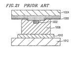
- As described in the above reports and shown in Figure 21, a vertical-cavity surface-emitting
laser 1002 obtained by interposing an emission thyrister having a p-n-p-n active layer between a pair of Bragg reflectors is formed on aGaAs substrate 1004, and asilicon nitride film 1006 is provided on the surface of theGaAs substrate 1004. AnAu layer 1008 with a thickness of 9 µm is formed on theGaAs substrate 1004 by a plating method so as to cover the entire portion of the vertical-cavity surface-emittinglaser 1002. The vertical-cavity surface-emittinglaser 1002 plated with Au is flip-chip mounted on anAlN heat sink 1012 including an Sn/Pb solder bump 1010. - In this structure, most of the heat generated in the vertical-cavity surface-emitting
laser 1002 is radiated from theAlN heat sink 1012 via theplated Au layer 1008 and the Sn/Pb solder bump 1010. Only a part of the heat is radiated directly from the Au into the air. The heat is further radiated directly from the active layer into theGaAs substrate 1004. - According to the conventional technique described above, the GaAs
substrate 1004 is bonded with theAlN heat sink 1012 by plastically molding the metal therebetween. Therefore, a load large enough to cause plastic to mold is required to be applied between theGaAs substrate 1004 and theAlN heat sink 1012. A part of the load is necessarily applied to the active layer of the vertical-cavity surface-emittinglaser 1002. However, the load applied to the active layer of the vertical-cavity surface-emittinglaser 1002 considerably degrades the emission efficiency of the laser. In a worst case, light can not be emitted from the laser at all. - In addition, the
solder bump 1010 made of Sn/Pb has a thermal conductivity one sixth as low as that of Au, so that the heat cannot be satisfactorily conducted in this portion. As a result, even if theAlN heat sink 1012 has a sufficiently high thermal conductivity, the heat cannot be satisfactorily radiated. - Furthermore, according to the conventional technique, the surface of the mesa of the vertical-cavity Surface-emitting
laser 1002 is required to be plated with Au. Therefore, an additional process must be performed. - The invention is defined in
claims - An optical module of a first aspect of this invention, includes : a first substrate; a vertical-cavity surface-emitting laser comprising an upper surface, a bottom surface and a semiconductor multi-layered structure including at least a light-emitting layer, the vertical-cavity surface-emitting laser being supported on the first substrate ; an electrode structure electrically connected with the bottom surface of the vertical-cavity surface-emitting laser, the electrode structure being supported on the first substrate ; and a second substrate comprising a first bump and a second bump, wherein an upper surface of the electrode structure and the upper surface of the vertical-cavity surface-emitting laser jut out from the first substrate, and the second substrate is positioned with respect to the first substrate so that the first bump and the second bump come into contact with an upper surface of the electrode structure and the upper surface of the vertical-cavity surface-emitting laser, respectively, wherein a principal portion of the electrode structure is made of the same material as the vertical-cavity surface-emitting laser, and the first substrate and the second substrate are adhered to each other, either by filling the gap therebetween with an adhesive or by forming an alloy between the bumps on the second substrate and the upper surface of structures on the first substrate.
- According to another embodiment of the first aspect of the invention, the principal portion of the electrode structure and the vertical-cavity surface-emitting laser is formed in the same crystal growth process.
- According to another embodiment of the first aspect of the invention, the optical module further comprises a transistor supported on the first substrate; and a third bump provided on the second substrate, wherein said third bump is partially in contact with the transistor.
- An optical module of a second aspect of the invention includes : a first substrate; a vertical-cavity surface-emitting laser comprising an upper surface, a bottom surface and a semiconductor multi-layered structure including at least a light-emitting layer, the vertical-cavity surface-emitting laser being supported on the first substrate; an electrode structure electrically connected with the bottom surface of the vertical-cavity surface-emitting laser, the electrode structure being supported on the first substrate; and a second substrate comprising a first bump and a second bump, wherein an upper surface of the electrode structure juts out from the first substrate, a first supporting structure comprising a conductive upper surface and being supported on the first substrate; and a first line for electrically connecting the upper surface of the vertical-cavity surface-emitting laser and the first supporting structure, the upper surface of the first supporting structure juts out from the first substrate, the second substrate is positioned with respect to the first substrate so that the first bump and the second bump come into contact with the upper surface of the electrode structure and the upper surface of the first supporting structure, respectively, and the first substrate and the second substrate are adhered to each other, either by filling the gap therebetween with an adhesive or by forming an alloy between the bumps on the second substrate and the upper surface of the structures on the first substrate.
- According to another embodiment of this aspect of the invention, a principal portion of the electrode structure is made of the same material as the vertical-cavity surface emitting laser.
- According to another embodiment of the invention, the first supporting structure is made of the same material as the vertical-cavity surface-emitting laser.
- According to another embodiment of this aspect of the invention the optical module further comprises : a transistor supported on the first substrate; a second supporting structure comprising a conductive upper surface and being formed on the first substrate; a second line for electrically connecting the transistor and the second supporting structure; and a third bump provided on the second substrate, wherein the third bump is in contact with the upper surface of the second supporting structure.
- An optical module of a third aspect of the invention comprises : a first substrate; a vertical-cavity surface-emitting laser comprising an upper surface, a bottom surface and a semiconductor multi-layered structure including at least a light-emitting layer, the vertical-cavity surface-emitting laser being supported on the first substrate; an electrode structure electrically connected with the bottom surface of the vertical-cavity surface-emitting laser, the electrode structure being supported on the first substrate; and a second substrate comprising a first bump and a second bump, wherein an upper surface of the electrode structure juts out from the first substrate; a principal portion of the electrode structure is made of the same material as the vertical-cavity surface-emitting laser, the optical module further includes a bipolar transistor formed on the upper surface of the vertical-cavity surface-emitting laser, the second substrate is positioned with respect to the first substrate so that the first bump and the second bump come into contact with an upper surface of the electrode structure and a portion of an upper surface of the bipolar transistor, respectively, and the first substrate and the second substrate are adhered to each other, either by filling the gap therebetween with an adhesive or by forming an alloy between the bumps on the second substrate and the upper surface of structures on the first substrate.
- An optical module of a fourth aspect of the invention comprises : a first substrate; a vertical-cavity surface-emitting laser comprising an upper surface, a bottom surface and a semiconductor multi-layer structure including at least a light-emitting layer, the vertical-cavity surface-emitting laser being supported on the first substrate; an electrode structure electrically connected with the bottom surface of the vertical-cavity surface-emitting laser, the electrode structure being supported on the first substrate; and a second substrate comprising a first bump and a second bump, wherein an upper surface of the electrode structure juts out from the first substrate, a bipolar transistor formed on the upper surface of the vertical-cavity surface-emitting laser; a first supporting structure comprising a conductive upper surface and being supported on the first substrate; and a first line for electrically connecting the bipolar transistor and the -upper surface of the first supporting structure, the upper surface of the first supporting structure juts out from the first substrate, the second substrate is positioned with respect to the first substrate so that the first bump and the second bump come into contact with the upper surface of the electrode structure and the upper surface of the first supporting structure, respectively, and the first substrate and the second substrate are adhered to each other, either by filling the gap therebetween with an adhesive or by forming an alloy between the bumps on the second substrate and the upper surface of structures on the first substrate.
- According to another embodiment of this aspect of the invention, a principal portion of the electrode structure is made of the same material as the vertical-cavity surface-emitting laser.
- According to another embodiment of the invention, the first supporting structure is formed close to the vertical-cavity surface-emitting laser.
- According to another embodiment of the invention, the first supporting structure comprises : semiconductor layers made of the same semiconductor materials as the semiconductor multi-layered structure; an insulating layer provided on the semiconductor layers; and an electrode provided on the insulating layer.
- According to another embodiment of the invention, the first supporting structure comprises : semiconductor layers made of the same semiconductor materials as the semiconductor multi-layered structure; and a metallic film provided on the semiconductor layers.
- According to another embodiment of the invention, a distance between the first substrate and the upper surface of the first supporting structure is longer than a distance between the first substrate and the upper surface of the vertical-cavity surface-emitting laser.
- According to another embodiment of the invention, the transistor is a field-effect transistor or a heterojunction bipolar transistor.
- According to another embodiment of the invention, a gap between the first substrate and the second substrate is filled with an adhesive. The adhesive is made of a thermosetting resin or an ultraviolet curable resin.
- According to another embodiment of the invention, the optical module comprises a plurality of electrode structures and a plurality of vertical-cavity surface-emitting lasers, wherein the plurality of electrode structures are disposed at respective vertexes of a polygon and the plurality of vertical-cavity surface-emitting lasers are disposed inside the polygon on the first substrate.
- According to another embodiment of the invention, the first bump and the second bump are made of a metal having a melting point of 350°c or lower.
- According to another embodiment of the invention, the upper surface of the electrode structure and the upper surface of the vertical-cavity surface-emitting laser are made of a metal having a melting point of 350°c or lower. The metal may be bismuth.
- According to another embodiment of the invention, the vertical-cavity surface-emitting laser further comprises a first distributed Bragg reflector and a second distributed Bragg reflector which are disposed so as to interpose the light-emitting layer therebetween.
- According to another embodiment of the invention, a guide groove to receive an optical fiber is provided in a reverse side of the first substrate in a portion corresponding to the position at which the vertical-cavity surface-emitting laser is provided.
- The present invention also concerns a method for fabricating such an optical module, comprising the steps of : growing, on a first substrate, a semiconductor multi-layered structure including a portion which is to function as a light-emitting layer of a vertical-cavity surface-emitting laser; forming an electrode structure on the first substrate; forming the vertical-cavity surface-emitting laser on the first substrate; forming a first bump and a second bump on a second substrate ; and positioning the second substrate with respect to the first substrate so that the first bump and the second bump come into contact with an upper surface of the electrode structure and an upper surface of the vertical-cavity surface-emitting laser, respectively, whereby the vertical-cavity surface-emitting laser and the electrode structure are both formed by etching the semiconductor multi-layered structure so that the upper surface of the electrode structure and the upper surface of the vertical-cavity surface-emitting laser jut out from the first substrate, a principal portion of the electrode structure is made of the same material as the vertical-cavity surface-emitting laser, and the first substrate and the second substrate are adhered to each other, either by filling the gap therebetween with an adhesive or by forming an alloy between the bumps on the second substrate and the upper surface of structures on the first substrate.
- Thus, the invention described herein makes possible the advantage of providing a surface-emitting laser device excellent in the radiation characteristics and the emission characteristics to be obtained by a mounting technique for bonding a vertical-cavity surface-emitting laser with a submount by applying a small load and eliminating the necessity of plating the laser with gold.
- This and other advantages of the present invention will become apparent to those skilled in the art upon reading and understanding the following detailed description with reference to the accompanying figures.
- Figure 1 is a cross-sectional view showing a configuration of an optical module according to a first example of the present invention.
- Figure 2 is a cross-sectional view showing a configuration of a vertical-cavity surface-emitting laser used for the optical module shown in Figure 1.
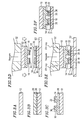
- Figures 3A to 3F are cross-sectional views illustrating a method for producing the optical module shown in Figure 1.
- Figures 4A and 4B are cross-sectional views showing a variant of the electrode structure used for the optical module of the first example.
- Figures 5A and 5B are perspective views showing the configurations of the first and the second substrates for constituting an optical module including a plurality of vertical-cavity surface-emitting lasers arranged in an array.
- Figures 6A and 6B are cross-sectional views showing a configuration of an optical module according to a second example of the present invention.
- Figure 7 is a graph showing an emission characteristic of the optical module shown in Figures 6A and 6B.
- Figure 8 is a cross-sectional view showing the interconnection between the optical module of the second example and an optical fiber.
- Figure 9 is a cross-sectional view showing a configuration of an optical module according to a third example of the present invention.
- Figure 10 is a cross-sectional view showing a configuration of another optical module according to the third example of the present invention.
- Figure 11 is a cross-sectional view showing a configuration of still another optical module according to the third example of the present invention.
- Figures 12A and 12B are cross-sectional views showing a configuration of an optical module according to a fourth example of the present invention.
- Figures 13A and 13B are cross-sectional views showing a configuration of another optical module according to the fourth example of the present invention.
- Figures 14A and 14B are cross-sectional views showing a configuration of still another optical module according to the fourth example of the present invention.
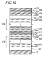
- Figure 15 is a cross-sectional view showing a configuration of the vertical-cavity surface-emitting laser used for the optical module shown in Figures 14A and 14B.
- Figures 16A to 16C are cross-sectional views illustrating a method for producing the optical module shown in Figure 15.
- Figure 17 is a cross-sectional view showing a configuration of an optical module according to a fifth example of the present invention.
- Figure 18 is a cross-sectional view showing a configuration of another optical module according to the fifth example of the present invention.
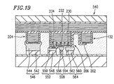
- Figure 19 is a cross-sectional view showing a configuration of still another optical module according to the fifth example of the present invention.
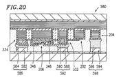
- Figure 20 is a cross-sectional view showing a configuration of still another optical module according to the fifth example of the present invention.
- Figure 21 is a cross-sectional view showing a configuration of a vertical-cavity surface-emitting laser obtaining by mounting a pair of substrates by a conventional method.
- Hereinafter, the present invention will be described by way of illustrative examples with reference to accompanying drawings.
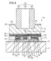
- Figure 1 is a cross-sectional view of an
optical module 10 according to an example of the present invention. Theoptical module 10 includes: afirst substrate 12 made of an n-type GaAs semiconductor; a vertical-cavity surface-emittinglaser 14 and anelectrode structure 16 which are supported by thefirst substrate 12; and asecond substrate 11 made of silicon. Thesecond substrate 11 functions as a submount. The surface of thesecond substrate 11 is covered with an insulatingfilm 21 made of silicon nitride, silicon oxide or the like, andmicro bumps second substrate 11 via the insulatingfilm 21. Though not shown in Figure 1, themicro bumps - The
upper surface 13 of the vertical-cavity surface-emittinglaser 14 and theupper surface 15 of theelectrode structure 16 jut out from thefirst substrate 12. The micro bumps 18 and 20 also jut out from thesecond substrate 11. As a result, thefirst substrate 12 and thesecond substrate 11 are positioned so that themicro bumps upper surface 13 of the vertical-cavity surface-emittinglaser 14 and theupper surface 15 of theelectrode structure 16, respectively. The gap between thefirst substrate 12 and thesecond substrate 11 is filled with an ultraviolet (UV)curable resin 22. - The vertical-cavity surface-emitting
laser 14 includes: a light-emittinglayer 24; a semiconductormulti-layered structure 30 including an n-type Bragg reflector 26 and a p-type Bragg reflector 28 which are provided so as to interpose the light-emittinglayer 24 therebetween; and anelectrode 32 provided on the semiconductormulti-layered structure 30. The light emitted from the light-emittinglayer 24 is preferably transparent to at least one of thefirst substrate 12 and thesecond substrate 11. In the case where the light emitted from the light-emittinglayer 24 is not transparent to thefirst substrate 12, agroove 90 can be provided at a region of the reverse surface of thefirst substrate 12 where the vertical-cavity surface-emittinglaser 14 is positioned. Thegroove 90 also enables emission of the light from the bottom thereof. - The
electrode structure 16 includes: a semiconductor multi-layered structure 34 consisting of the same semiconductor layers as those of the semiconductormulti-layered structure 30; and anelectrode 36 provided on the semiconductor multi-layered structure 34. The p-n junction formed in the semiconductor multi-layered structure 34 has been broken and theupper surface 15 and thebottom surface 19 of theelectrode structure 16 are connected with each other at a low resistance. The vertical-cavity surface-emittinglaser 14 and theelectrode structure 16 are provided on thefirst substrate 12 via abuffer layer 38 made of n-type GaAs with a low resistance. Therefore, thebottom surface 17 of the vertical-cavity surface-emittinglaser 14 and thebottom surface 19 of theelectrode structure 16 are in contact with thebuffer layer 38, and are electrically connected with each other. - The micro bumps 18 and 20 are preferably made of a material excellent in the thermal conductivity. More preferably, the material contains Au excellent in the thermal conductivity.
- Referring to Figure 2, a more detailed structure of the vertical-cavity surface-emitting
laser 14 will be described. As shown in Figure 2, the n-type Bragg reflector 26 includes 24.5 pairs of alternately stacked layers consisting of n-type AlAs layers 41 and n-type GaAs layers 42. In the same way, the p-type Bragg reflector 28 includes 24.5 pairs of alternately stacked layers consisting of p-type AlAs layers 43 and p-type GaAs layers 44. Anactive region 45 is provided between the n-type Bragg reflector 26 and the p-type Bragg reflector 28. - The
active region 45 includes: a light-emittinglayer 24; a pair of barrier layers 46 and 47; and spacer layers 48, 49, 50 and 51. The light-emittinglayer 24 is interposed between the pair of barrier layers 46 and 47, and the barrier layers 46 and 47 are interposed between two pairs of spacer layers 48 / 50 and 49 / 51. The light-emittinglayer 24 and the barrier layers 46 and 47 are made of undoped In0.2Ga0.8As and undoped GaAs, respectively. The spacer layers 48 and 49 are made of undoped Al0.5Ga0.5As and the spacer layers 50 and 51 are made of an n-type Al0.5Ga0.5As and p-type Al0.5Ga0.5As, respectively. The electrons and the holes are collected in the light-emittinglayer 24 by the barrier layers 46 and 47. The spacer layers 48, 49, 50 and 51 are provided in order to adjust the length of the vertical cavity of the laser and obtain a laser oscillation in a single longitudinal mode. The thicknesses of these semiconductor layers and the impurity concentrations thereof are shown in following Table 1.Layer Composition Thickness (nm) Impurity concentration (cm-3) p-type GaAs layer 44 p-GaAs 69.6 Be: 1x10¹⁸ p-type AlAs layer 43 p-AlAs 82.8 Be: 1x10¹⁸ spacer layer 51 p-Al0.5Ga0.5As 86 Be: 1.5x10¹⁸ spacer layer 49 u-Al0.5Ga0.5As 50 barrier layer 47u-GaAs 10 light-emitting layer 24u-In0.2Ga0.8As 8 barrier layer 46u-GaAs 10 spacer layer 48u-Al0.5Ga0.5As 50 spacer layer 50 n-Al0.5Ga0.5As 86 Si: 1.5x10¹⁸ n-type GaAs layer 42 n-GaAs 69.6 Si: 1x10¹⁸ n-type AlAs layer 41 n-AlAs 82.8 Si: 1x10¹⁸ - Referring to Figure 1 again, in the
optical module 10, a positive power supply and a negative power supply are connected with the lines connected with themicro bump 18 and the lines connected with themicro bump 20, respectively, so that a positive voltage is applied to theelectrode 32 of the vertical-cavity surface-emittinglaser 14 while a negative voltage is applied to theelectrode 36 of theelectrode structure 16. - Since the
electrode structure 16 is electrically connected with thebottom surface 17 of the vertical-cavity surface-emittinglaser 14 via thebuffer layer 38, a positive voltage and a negative voltage are applied to the p-type distributedBragg reflector 28 and the n-type distributedBragg reflector 26, respectively. As a result, the vertical-cavity surface-emittinglaser 14 can emit light. - The
optical module 10 is produced, for example, by the following method. - First, as shown in Figures 3A and 3B, a
buffer layer 38 and a semiconductormulti-layered structure 30 including the semiconductor layers 24 and 41 to 51 shown in Figure 2 are epitaxially grown on afirst substrate 12 made of n-type GaAs by a molecular beam epitaxy (MBE) method or the like. Next, as shown in Figure 3C, the semiconductormulti-layered structure 30 is partially etched by a dry etching method using a mixture gas containing chlorine until thebuffer layer 38 is exposed. Then,electrodes multi-layered structure 30, thereby forming a vertical-cavity surface-emittinglaser 14 and anelectrode structure 16. The p-n junction in the semiconductormulti-layered structure 30 forming theelectrode structure 16 is broken beforehand by applying a high electric field between thebuffer layer 38 and theelectrode 36. As a result, theelectrode structure 16 with a low resistance can be formed. - Next, as shown in Figure 3D, an insulating
film 21 made of silicon oxide is formed on thesecond substrate 11 made of silicon positioned on a supportingplate 53, andmicro bumps micro bumps curable resin 22 is applied onto the insulatingfilm 21 so as to cover themicro bumps first substrate 12 is stuck onto avacuum collet 52, and then positioned with respect to thesecond substrate 11 so that themicro bumps laser 14 and theelectrode structure 16, respectively. - Next, as indicated by the arrow shown in Figure 3D, the
first substrate 12 is pressed against thesecond substrate 11 so that theupper surface 13 of theelectrode 32 on the vertical-cavity surface-emittinglaser 14 and theupper surface 15 of theelectrode 36 on theelectrode structure 16 come into contact with themicro bumps curable resin 22 between themicro bump 18 and the vertical-cavity surface-emittinglaser 14 and between themicro bump 20 and theelectrode structure 16 is removed. While maintaining this state, the UVcurable resin 22 is irradiated with UV rays. The irradiation of the UV rays causes the shrinkage of the UVcurable resin 22 and attaches thefirst substrate 12 and thesecond substrate 11 with each other. Theelectrode 32 on the vertical-cavity surface-emittinglaser 14 and theelectrode 36 on theelectrode structure 16 securely come into contact with themicro bumps electrodes micro bumps electrodes micro bumps optical module 10 shown in Figure 3F is completed. - According to the present invention, the
first substrate 12 and thesecond substrate 11 are attached with the shrinkage force of the UVcurable resin 22 exerted to the entire portion of thefirst substrate 12 and thesecond substrate 11. Therefore, it is possible to reduce the load applied to the upper surface of the vertical-cavity surface-emitting laser, and reduce the distortion to be given to the light-emittinglayer 24 by the load during the mounting process, thereby preventing the decrease in the emission efficiency. In addition, the heat generated in the light-emitting layer can be radiated through the micro bumps into the second substrate, thereby realizing excellent radiation characteristics. - In the above-described example, the
electrode structure 16 consists of the semiconductor multi-layered structure 34 in which the p-n junction has been broken and the electrode formed on the semiconductor multi-layered structure 34. Alternatively, theelectrode structure 16 can be an other type of conductive structure. Hereinafter, another exemplary electrode structure will be described in detail. - An
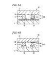
optical module 58 shown in Figure 4A includes an electrode structure 60 instead of theelectrode structure 16 shown in Figure 1. The electrode structure 60 includes: a body 61 constituted by a semiconductor multi-layered structure, an insulating layer or the like; and a conductive layer 62 provided at the surface of the body 61 so as to cover the upper and side surfaces thereof and electrically connected at least with thebuffer layer 38. In order to obtain a low-resistance electrical contact between the conductive layer 62 and thebuffer layer 38, the conductive layer 62 is preferably made of an ohmic electrode material such as AuGe/Ni or AuZn/Au. - An
optical module 59 shown in Figure 4B includes an electrode structure 63 instead of theelectrode structure 16 shown in Figure 1. The electrode structure 63 includes: anohmic electrode 64 formed on thebuffer layer 38 and anAu layer 65 formed on theohmic electrode 64 by a plating method. - In this example, an ultraviolet curable resin is used as an adhesive. Alternatively, a thermosetting resin can also be used.
- The optical module of this example includes one vertical-cavity surface-emitting laser and one electrode structure. However, the optical module can include two or more vertical-cavity surface-emitting lasers and electrode structures.
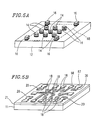
- Figures 5A and 5B are perspective views showing the configurations of the
first substrate 12 and thesecond substrate 11 for constituting an optical module including nine vertical-cavity surface-emittinglasers 14 and fourelectrode structures 16. - As shown in Figure 5A, nine vertical-cavity surface-emitting
lasers 14 arranged in the three rows and three columns are supported on thefirst substrate 12. The fourelectrode structures 16 are disposed at the four vertexes of therectangle 68 surrounding the array of the vertical-cavity surface-emittinglasers 14. - As shown in Figure 5B,
micro bumps second substrate 11 via the insulatingfilm 21 at the positions corresponding to those of the vertical-cavity surface-emittinglasers 14 and theelectrode structures 16 provided on thefirst substrate 12. Thelines micro bumps - By disposing the vertical-cavity surface-emitting
lasers 14 and theelectrode structures 16 as shown in Figure 5A, the load to be applied during the bonding of thefirst substrate 12 with thesecond substrate 11 is uniformly dispersed among the fourelectrode structures 16. Accordingly, when the vertical-cavity surface-emittinglasers 14 come into contact with themicro bumps 18, the vertical-cavity surface-emittinglasers 14 receive a uniform load, so that the degradation of the emission efficiency of the vertical-cavity surface-emittinglasers 14 can be suppressed as compared with the case of using the vertical-cavity surface-emittinglaser 14 shown in Figure 1. - Figures 6A and 6B are cross-sectional views of an
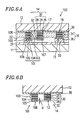
optical module 100 according to a second example of the present invention. In Figures 6A and 6B, the same components as those of theoptical module 10 shown in Figure 1 will be denoted by the same reference numerals. - The
optical module 100 includes: afirst substrate 12; a vertical-cavity surface-emittinglaser 14, anelectrode structure 16 and a supportingstructure 101 which are supported by thefirst substrate 12 via abuffer layer 38; and asecond substrate 11. The surface of thesecond substrate 11 is covered with an insulatingfilm 21 made of silicon nitride, silicon oxide or the like, andmicro bumps second substrate 11 via the insulatingfilm 21. Though not shown in Figure 6A, themicro bumps - The vertical-cavity surface-emitting
laser 14 includes: a light-emittinglayer 24; a semiconductormulti-layered structure 30 including an n-type distributedBragg reflector 26 and a p-type distributedBragg reflector 28 which are provided so as to interpose the light-emittinglayer 24 therebetween; and anelectrode 32 provided on the semiconductormulti-layered structure 30. - The
electrode structure 16 includes: a semiconductor multi-layered structure 34 consisting of the same semiconductor layers as those of the semiconductormulti-layered structure 30; and anelectrode 36 provided on the semiconductor multi-layered structure 34. The p-n junction formed in the semiconductor multi-layered structure 34 has been broken and theupper surface 15 and thelower surface 19 of theelectrode structure 16 are connected with each other at a low resistance. - The supporting
structure 101 includes a semiconductormulti-layered structure 103 consisting of the same semiconductor layers as those of the semiconductormulti-layered structure 30. An insulatinglayer 104 is provided between the semiconductormulti-layered structure 103 and theelectrode 105. The supportingstructure 101 can be made of any material other than the material of the semiconductormulti-layered structure 103 so long as theupper surface 108 of the supportingstructure 101 has a conductance and the portion between thebuffer layer 38 on which the supportingstructure 101 is formed and theupper surface 108 is electrically insulated. - A
polyimide film 106 is provided so as to cover thebuffer layer 38 on thefirst substrate 12. Aline 107 is provided on thepolyimide film 106 for electrically connecting theelectrode 32 of the vertical-cavity surface-emittinglaser 14 and theelectrode 105 of the supportingstructure 101. Thepolyimide film 106 is provided principally for retaining theline 107 at a predetermined distance from the surface of thefirst substrate 12, so that the difference in the height between theelectrodes line 107 caused by the discontinuity of theline 107 owing to the difference in the height between theelectrodes - The
upper surface 108 of the supportingstructure 101 and theupper surface 15 of theelectrode structure 16 jut out from thefirst substrate 12, and thefirst substrate 12 and thesecond substrate 11 are positioned so that themicro bumps upper surface 15 of theelectrode structure 16 and theupper surface 108 of the supportingstructure 101. The gap between thepolyimide film 106 and thesecond substrate 11 is filled with a UVcurable resin 22. - In the
optical module 100, a positive power supply and a negative power supply are connected with the lines connected with themicro bump 102 and the lines connected with themicro bump 20, respectively, so that a positive voltage is applied to theline 107 while a negative voltage is applied to theelectrode structure 16. - Since the
line 107 is electrically connected with theelectrode 32 of the vertical-cavity surface-emittinglaser 14, and theelectrode structure 16 is electrically connected with thebottom surface 17 of the vertical-cavity surface-emittinglaser 14 via thebuffer layer 38; a positive voltage and a negative voltage are applied to the p-type distributedBragg reflector 28 and the n-type distributedBragg reflector 26, respectively. As a result, the vertical-cavity surface-emittinglaser 14 can emit light. - A principal feature of the
optical module 100 lies in that theelectrode structure 16 and the supportingstructure 101 provided on thefirst substrate 12 are received by themicro bumps second substrate 11. By using such a configuration, thefirst substrate 12 can be bonded with thesecond substrate 11 without applying a load to the vertical-cavity surface-emittinglaser 14. Therefore, the vertical-cavity surface-emittinglaser 14 can be mounted on the submount without applying a load to the light-emittinglayer 24 of the vertical-cavity surface-emittinglaser 14 and degrading the emission efficiency of thelaser 14. In order to unfailingly not apply the load during the bonding to the vertical-cavity surface-emittinglaser 14, the supportingstructure 101 is preferably disposed close to the vertical-cavity surface-emittinglaser 14, e.g., at a distance of 20 µm or less from the vertical-cavity surface-emittinglaser 14. Theelectrodes micro bumps electrodes micro bumps - In addition, in order to unfailingly not apply a load to the vertical-cavity surface-emitting
laser 14, theupper surface 108 of the supportingstructure 101 is preferably higher than theupper surface 13 of the vertical-cavity surface-emittinglaser 14 with respect to thebuffer layer 38, as shown in Figure 6B. Such a configuration can be realized by making the sum of the thickness of the insulatinglayer 104 and that of theelectrode 105 larger than the thickness of theelectrode 32. The difference in the height between theupper surfaces structure 101 is engaged into themicro bump 102, it is possible to unfailingly prevent both the contact between theupper surface 13 of the vertical-cavity surface-emittinglaser 14 and the insulatingfilm 21, and the application of a load to the light-emittinglayer 24. - The
optical module 100 is produced by almost the same method as that for producing theoptical module 10 of the first example. - More specifically, when the semiconductor
multi-layered structure 30 of the vertical-cavity surface-emittinglaser 14 is formed by the D/E method, the semiconductor multi-layered structure 34 for theelectrode structure 16 and the semiconductormulti-layered structure 103 for the supportingstructure 101 are simultaneously formed. Thereafter, the insulatinglayer 104 is formed on the semiconductormulti-layered structure 103 and theelectrodes multi-layered structures 30 and 34 and the insulatinglayer 104, respectively. After thepolyimide film 106 is formed so as to cover thebuffer layer 38, theline 107 for connecting theelectrodes second substrate 11 is bonded with thefirst substrate 12 in the same way as in the first example. - In the
optical module 100, theelectrode structure 16 and the UVcurable resin 22 can be modified in various manners as described in the first example. - Figure 7 is a graph showing an exemplary output power characteristic of the
optical module 100 produced in the above-described manner. The output power characteristic of thelaser device 100 before bonding the second substrate is also shown in Figure 7 for comparison. As is apparent from Figure 7, the maximum output power is about 21 mW before bonding the second substrate. On the other hand, after the second substrate is bonded, the maximum output power increases up to about 32 mW. This is because the emission efficiency can be improved by bonding the second substrate with the first substrate via the micro bumps. That is to say, the heat generated in the vertical-cavity surface-emitting laser has been radiated through thepolyimide film 106 and the UVcurable resin 22 into thefirst substrate 12 and thesecond substrate 11. - The optical module having the above-described configuration can be suitably combined with an optical fiber. Figure 8 schematically shows the cross section of an
optical module 110 which can be connected with an optical fiber. - The
optical module 110 includes: afirst substrate 12; a vertical-cavity surface-emittinglaser 111, anelectrode structure 112 and a supportingstructure 113 which are supported by thefirst substrate 12; and asecond substrate 11. The surface of thesecond substrate 11 is covered with an insulatingfilm 21 made of silicon nitride, silicon oxide or the like, andmicro bumps second substrate 11 via the insulatingfilm 21. Though not shown in Figure 8, themicro bumps - The vertical-cavity surface-emitting
laser 111 includes: a light-emittinglayer 24; a semiconductormulti-layered structure 115 including an n-type distributedBragg reflector 26 and a part of a p-type distributedBragg reflector 114 which are provided so as to interpose the light-emittinglayer 24 therebetween; and anelectrode 32 provided on the semiconductormulti-layered structure 115. The p-type distributedBragg reflector 114 is formed so as to cover the entire surface of thefirst substrate 12. - The
electrode structure 112 includes: a semiconductormulti-layered structure 116 consisting of the same semiconductor layers as those of the semiconductormulti-layered structure 115; and anelectrode 36 provided on the semiconductormulti-layered structure 116. The semiconductormulti-layered structure 116 includes a part of the p-type distributedBragg reflector 114 and the p-n junction formed in the semiconductormulti-layered structure 116 has been broken. - The supporting
structure 113 includes: a semiconductormulti-layered structure 117 consisting of the same semiconductor layers as those of the semiconductormulti-layered structure 115; a part of an insulatinglayer 118 covering the semiconductormulti-layered structure 117; and a part of theline 119 provided on the insulatinglayer 118. The insulatinglayer 118 is further formed on the p-type distributedBragg reflector 114 so as to cover the sides of the vertical-cavity surface-emittinglaser 111 and theelectrode structure 112. Theline 119 is connected with theelectrode 32 of the vertical-cavity surface-emittinglaser 111. - The
upper surface 15 of theelectrode structure 112 and theupper surface 120 of the supportingstructure 113 jut out from thefirst substrate 12. Thefirst substrate 12 and thesecond substrate 11 are positioned so that themicro bumps upper surface 15 of theelectrode structure 112 and theupper surface 120 of the supportingstructure 113. The gap between thefirst substrate 12 and thesecond substrate 11 is filled with a UVcurable resin 22. - A guiding
groove 121 is provided in a reverse side 126 of thefirst substrate 12 in a portion corresponding to the position at which the vertical-cavity surface-emittinglaser 111 is provided, and asilicon oxide film 122 is formed around the guidinggroove 121. A multi-modeoptical fiber 123 including acore 124 and acladding layer 125, is inserted into the guidinggroove 121. The light 127 emitted from the vertical-cavity surface-emittinglaser 111 is transmitted through thefirst substrate 12 and then incident onto thecore 124. - By using such a configuration, all the lines required for driving the vertical-cavity surface-emitting
laser 111 can be formed on thesecond substrate 11, and a space for connecting the optical fiber can be secured in the reverse side 126 of thefirst substrate 12. In addition, it is easy to align the multi-modeoptical fiber 123 with the vertical-cavity surface-emittinglaser 111 since the guidinggroove 121 having a large depth can be provided in the reverse side 126 of thefirst substrate 12. Accordingly, even if a plurality of vertical-cavity surface-emittinglasers 111 are arranged in an array on thefirst substrate 12, a plurality of optical fibers can be easily connected with thelasers 111, thereby providing anoptical module 110 suitable for being interconnected with an optical fiber. - Figure 9 is a cross-sectional view of a an
optical module 130 according to a third example of the present invention. Theoptical module 130 includes: afirst substrate 12; a vertical-cavity surface-emittinglaser 132, anelectrode structure 136 and a field-effect transistor (hereinafter, simply referred to as an "FET") 134 which are supported by thefirst substrate 12; and asecond substrate 11. The surface of thesecond substrate 11 is covered with an insulatingfilm 21 made of silicon nitride, silicon oxide or the like, andmicro bumps second substrate 11 via the insulatingfilm 21. Though not shown in Figure 9, themicro bumps - The vertical-cavity surface-emitting
laser 132 includes: a light-emittinglayer 24; a semiconductormulti-layered structure 148 including a part of an n-type distributedBragg reflector 144 and a p-type distributedBragg reflector 146 which are provided so as to interpose the light-emittinglayer 24 therebetween; and anelectrode 150 provided on the semiconductormulti-layered structure 148. The n-type distributedBragg reflector 144 is formed so as to cover the entire surface of thefirst substrate 12. - The
FET 134 includes: an n-type channel layer 154; agate electrode 156 provided on the n-type channel layer 154; asource electrode 158; and adrain electrode 160. Thechannel layer 154 is formed on the semiconductormulti-layered structure 152 consisting of the same semiconductor layers as those of the semiconductormulti-layered structure 148. - The
electrode structure 136 includes: a semiconductormulti-layered structure 162 consisting of the same semiconductor layers as those of the semiconductormulti-layered structure 152 and thechannel layer 154; and anelectrode 164 provided on the semiconductormulti-layered structure 162. The semiconductormulti-layered structure 162 includes a part of the n-type distributedBragg reflector 144 and the p-n junction formed in the semiconductormulti-layered structure 162 has been broken. As a result, theupper surface 166 of theelectrode structure 136 is connected with the n-type distributedBragg reflector 144 of the vertical-cavity surface-emittinglaser 132 at a low resistance. - The sides of the vertical-cavity surface-emitting
laser 132, theFET 134 and theelectrode structure 136 and the surface of the n-type distributedBragg reflector 144 are covered with an insulatingfilm 168 made of silicon oxide, silicon nitride or the like. Aline 170 for electrically connecting theelectrode 150 of the vertical-cavity surface-emittinglaser 132 with thesource electrode 158 is provided on the insulatingfilm 168. - The
upper surface 166 of theelectrode structure 136 juts out from the n-type distributedBragg reflector 144 formed on thefirst substrate 12. Thefirst substrate 12 and thesecond substrate 11 are positioned so that themicro bumps upper surface 166 of theelectrode structure 136, thedrain electrode 160 and thegate electrode 156, respectively. The gap between thefirst substrate 12 and thesecond substrate 11 is filled with a UVcurable resin 22. - In the
optical module 130, a current flows between thedrain electrode 160 and thesource electrode 158 based on the voltage applied to thegate electrode 156, and a voltage is applied to the vertical-cavity surface-emittinglaser 132 via theline 170. On the other hand, a voltage is also applied to the n-type distributedBragg reflector 144 via theelectrode structure 136, so that the vertical-cavity surface-emittinglaser 132 can emit light. - In this configuration, since the
upper surface 172 of the vertical-cavity surface-emittinglaser 132 does not come into contact with the micro bumps, it is possible to bond thesecond substrate 11 with thefirst substrate 12 without applying a load to the light-emittinglayer 24. - In the above-described example, the optical module includes a field-effect transistor. As will be described below, a heterojunction bipolar transistor can be used instead of the field-effect transistor.
- Figure 10 is a cross-sectional view of a an
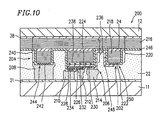
optical module 200. Theoptical module 200 includes: afirst substrate 12; a vertical-cavity surface-emittinglaser 202, anelectrode structure 204 and a heterojunctionbipolar transistor 206 which are supported by thefirst substrate 12 via abuffer layer 38; and asecond substrate 11. The surface of thesecond substrate 11 is covered with an insulatingfilm 21 made of silicon nitride, silicon oxide or the like, andmicro bumps second substrate 11 via the insulatingfilm 21. Though not shown in Figure 10, themicro bumps - The vertical-cavity surface-emitting
laser 202 includes: a light-emittinglayer 24; a semiconductormulti-layered structure 220 including a part of a p-type distributedBragg reflector 216 and an n-type distributedBragg reflector 218 which are provided so as to interpose the light-emittinglayer 24 therebetween; and anelectrode 222 provided on the semiconductormulti-layered structure 220. The p-type distributedBragg reflector 216 is formed so as to cover the entire surface of thebuffer layer 38. - The heterojunction
bipolar transistor 206 includes: acollector layer 224; abase layer 226; anemitter layer 228; and acollector electrode 230, abase electrode 232 and anemitter electrode 234 electrically connected with thesesemiconductor layers base layer 226 is interposed between theemitter layer 228 and thecollector layer 224. Thecollector layer 224 is formed on the semiconductormulti-layered structure 236 consisting of the same semiconductor layers as those of the semiconductormulti-layered structure 220 via abuffer layer 238. - The
electrode structure 204 includes: a semiconductormulti-layered structure 240 consisting of the same semiconductor layers as those of the semiconductormulti-layered structure 220; and anelectrode 242 provided on the semiconductormulti-layered structure 240. The semiconductormulti-layered structure 240 includes a part of the p-type distributedBragg reflector 216 and the p-n junction formed in the semiconductormulti-layered structure 240 has been broken. As a result, theupper surface 244 of theelectrode structure 204 is connected with the p-type distributedBragg reflector 216 of the vertical-cavity surface-emittinglaser 202 at a low resistance. - The sides of the vertical-cavity surface-emitting
laser 202, the heterojunctionbipolar transistor 206, and theelectrode structure 204 and the surface of the p-type distributedBragg reflector 216 are covered with an insulatingfilm 246 made of silicon oxide, silicon nitride or the like. Aline 248 for electrically connecting theelectrode 222 of the vertical-cavity surface-emittinglaser 202 with thecollector electrode 230 is provided on the insulatingfilm 246. - The
upper surface 244 of theelectrode structure 204 juts out from the p-type distributedBragg reflector 216 formed on thefirst substrate 12. Thefirst substrate 12 and thesecond substrate 11 are positioned so that themicro bumps upper surface 244 of theelectrode structure 204, theemitter electrode 234, thebase electrode 232 and thecollector electrode 230, respectively. The gap between thefirst substrate 12 and thesecond substrate 11 is filled with a UVcurable resin 22. - In the
optical module 200, a current flows between theemitter electrode 234 and thecollector electrode 230 based on the voltage or the current applied to thebase electrode 232 via the micro bump 212, and a voltage is applied to the n-type distributedBragg reflector 218 of the vertical-cavity surface-emittinglaser 202 via theline 248. On the other hand, a voltage is also applied to the p-type distributedBragg reflector 216 via theelectrode structure 204, so that the vertical-cavity surface-emittinglaser 202 can emit light. - In this configuration, since the
upper surface 250 of the vertical-cavity surface-emittinglaser 202 does not come into contact with the micro bumps, it is possible to bond thesecond substrate 11 with thefirst substrate 12 without applying a load to the light-emittinglayer 24. - In addition, as will be described below, the heterojunction bipolar transistor can be formed on the vertical-cavity surface-emitting laser.
- Figure 11 is a cross-sectional view of an
optical module 260. Theoptical module 260 includes: afirst substrate 12; a vertical-cavity surface-emittinglaser 262 and anelectrode structure 264 which are supported by thefirst substrate 12 via abuffer layer 38; a heterojunctionbipolar transistor 266 formed on the vertical-cavity surface-emittinglaser 262; and asecond substrate 11. The surface of thesecond substrate 11 is covered with an insulatingfilm 21 made of silicon nitride, silicon oxide or the like, andmicro bumps second substrate 11 via the insulatingfilm 21. Though not shown in Figure 11, themicro bumps - The vertical-cavity surface-emitting
laser 262 includes: a light-emittinglayer 24; and a part of a p-type distributedBragg reflector 276 and an n-type distributedBragg reflector 278 which are provided so as to interpose the light-emittinglayer 24 therebetween. The p-type distributedBragg reflector 276 is formed so as to cover the entire surface of thebuffer layer 38. - The heterojunction
bipolar transistor 266 includes: acollector layer 280; abase layer 282; anemitter layer 284;base electrodes base layer 282; and anemitter electrode 288 electrically connected with theemitter layer 284. Thebase layer 282 is interposed between theemitter layer 284 and thecollector layer 280. Thecollector layer 280 is formed on the n-type distributedBragg reflector 278 of the vertical-cavity surface-emittinglaser 262. - The
electrode structure 264 includes: a semiconductormulti-layered structure 290 consisting of the same semiconductor layers as those of the vertical-cavity surface-emittinglaser 262; and anelectrode 292 provided on the semiconductormulti-layered structure 290. The semiconductormulti-layered structure 290 includes a part of the p-type distributedBragg reflector 276 and the p-n junction formed in the semiconductormulti-layered structure 290 has been broken. As a result, theupper surface 294 of theelectrode structure 264 is connected with the p-type distributedBragg reflector 276 of the vertical-cavity surface-emittinglaser 262 at a low resistance. - The sides of the vertical-cavity surface-emitting
laser 262, the heterojunctionbipolar transistor 266, and theelectrode structure 264 and the surface of the p-type distributedBragg reflector 276 are covered with an insulatingfilm 296 made of silicon oxide, silicon nitride or the like. - The
upper surface 294 of theelectrode structure 264 juts out from thefirst substrate 12, and thefirst substrate 12 and thesecond substrate 11 are positioned so that themicro bumps base electrode 286, theemitter electrode 288, thebase electrode 287 and theupper surface 294 of theelectrode structure 264, respectively. The gap between thefirst substrate 12 and thesecond substrate 11 is filled with a UVcurable resin 22. - In the
optical module 260, negative charges are applied from themicro bump 270 to the n-type distributedBragg reflector 278 via theemitter layer 284, thebase layer 282 and thecollector layer 280 based on the voltage applied from themicro bumps base layer 282 via thebase electrodes micro bump 274 to the p-type distributedBragg reflector 276 via theelectrode structure 264, so that the vertical-cavity surface-emittinglaser 262 can emit light. - In the above-explained example, the optical module includes at least two micro bumps provided on the second substrate so as to receive at least two terminals of an FET or a bipolar transistor. However, it is not necessary to provide an optical module of the present invention with a micro bump which directly receives such a terminal of a transistor. For example, in the case where an optical module further includes an active element or passive element, the terminals of a transistor can connected with the active elements or the passive element and do not have to be directly connected with micro bumps formed on the second substrate.
- Figure 12A is a cross-sectional view of an
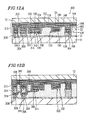
optical module 300 according to a fourth example of the present invention. Theoptical module 300 is different from theoptical module 130 shown in Figure 9 in that theoptical module 300 includes two supporting structures and that the micro bumps are not directly in contact with the field-effect transistor. In Figure 12A, the same components as those of theoptical module 130 shown in Figure 9 will be denoted by the same reference numerals. - The
optical module 300 includes: afirst substrate 12; a vertical-cavity surface-emittinglaser 132, anelectrode structure 136, a field-effect transistor 134, a first supportingstructure 302 and a second supportingstructure 304 which are supported by thefirst substrate 12; and asecond substrate 11. The surface of thesecond substrate 11 is covered with an insulatingfilm 21 made of silicon nitride, silicon oxide or the like, andmicro bumps second substrate 11 via the insulatingfilm 21. Though not shown in Figure 12A, themicro bumps - The vertical-cavity surface-emitting
laser 132 includes: a light-emittinglayer 24; a semiconductormulti-layered structure 148 including a part of an n-type distributedBragg reflector 144 and a p-type distributedBragg reflector 146 which are provided so as to interpose the light-emittinglayer 24 therebetween; and anelectrode 150 provided on the semiconductormulti-layered structure 148. The n-type distributedBragg reflector 144 is formed so as to cover the entire surface of thefirst substrate 12. - The
FET 134 includes: an n-type channel layer 154; and agate electrode 156, asource electrode 158 and adrain electrode 160 provided on the n-type channel layer 154. Thechannel layer 154 is formed on the semiconductormulti-layered structure 152 consisting of the same semiconductor layers as those of the semiconductormulti-layered structure 148. - The
electrode structure 136 includes: a semiconductormulti-layered structure 162 consisting of the same semiconductor layers as those of the semiconductormulti-layered structure 148 and thechannel layer 154; and anelectrode 164 provided on the semiconductormulti-layered structure 162. The semiconductormulti-layered structure 162 includes a part of the n-type distributedBragg reflector 144 and the p-n junction formed in the semiconductormulti-layered structure 162 has been broken. As a result, theupper surface 166 of theelectrode structure 136 is connected with the n-type distributedBragg reflector 144 of the vertical-cavity surface-emittinglaser 132 at a low resistance. - The first supporting
structure 302 and the second supportingstructure 304 include: semiconductormulti-layered structures multi-layered structure 148 and thechannel layer 154; a part of the insulatinglayer 168 covering the semiconductormulti-layered structures lines layer 168. Thelines drain electrode 160 and thegate electrode 156, respectively. - The sides of the vertical-cavity surface-emitting
laser 132, theFET 134, theelectrode structure 136, the first supportingstructure 302 and the second supportingstructure 304 and the surface of the n-type distributedBragg reflector 144 are covered with an insulatingfilm 168 made of silicon oxide, silicon nitride or the like. Aline 170 for electrically connecting theelectrode 150 of the vertical-cavity surface-emittinglaser 132 with thesource electrode 158 is provided on the insulatingfilm 168. - The upper surfaces of the
electrode structure 136, the first supportingstructure 302, and the second supportingstructure 304 jut out from thefirst substrate 12. Thefirst substrate 12 and thesecond substrate 11 are positioned so that themicro bumps upper surface 166 of theelectrode structure 136, the upper surface of the first supportingstructure 302, and the upper surface of the second supportingstructure 304, respectively. The gap between thefirst substrate 12 and thesecond substrate 11 is filled with a UVcurable resin 22. - In the
optical module 300, a voltage is applied from themicro bump 306 to the p-type distributedBragg reflector 146 of the vertical-cavity surface-emittinglaser 132 via theline 314, thedrain electrode 160, thesource electrode 158 and theline 170 based on the voltage applied from themicro bump 308 to theline 316 and thegate electrode 156. On the other hand, a voltage is also applied to the n-type distributedBragg reflector 144 via theelectrode structure 136, so that the vertical-cavity surface-emittinglaser 132 can emit light. - In this configuration, since the upper surface of the vertical-cavity surface-emitting
laser 132 does not come into contact with the micro bumps, it is possible to bond thesecond substrate 11 with thefirst substrate 12 without applying a load to the light-emittinglayer 24 or theFET 134. - In addition, in order to unfailingly not apply a load to the vertical-cavity surface-emitting
laser 132, theupper surfaces structures upper surface 322 of the vertical-cavity surface-emittinglaser 132, as shown in Figure 12B. Such a configuration can be realized by providing an insulatinglayer 324 made of silicon oxide, silicon nitride or the like with an appropriate thickness between the semiconductormulti-layered structure 310 and the insulatinglayer 168 and between the semiconductormulti-layered structure 312 and the insulatinglayer 168. The difference in the height between theupper surfaces upper surfaces lines polyimide resin 326 on the insulatinglayer 168 and reduce the difference in the heights. In this configuration, even when the first and the second supportingstructures micro bumps upper surface 322 of the vertical-cavity surface-emittinglaser 132 and thesecond substrate 11 and the application of a load to the light-emittinglayer 24. - In the above-described example, the optical module includes a field-effect transistor. Alternatively, the optical module can include a heterojunction bipolar transistor instead of the field-effect transistor as will be described below.
- Figure 13A is a cross-sectional view of an
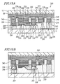
optical module 330. Theoptical module 330 is different from theoptical module 200 shown in Figure 10 in that theoptical module 330 includes two supporting structures and that the micro bumps are not in contact with the heterojunction bipolar transistor. In Figure 13A, the same components as those of theoptical module 200 shown in Figure 10 will be denoted by the same reference numerals. - The
optical module 330 includes: afirst substrate 12; a vertical-cavity surface-emittinglaser 202, anelectrode structure 204, a first supportingstructure 332, a second supportingstructure 334, and a heterojunctionbipolar transistor 206 which are supported by thefirst substrate 12 via abuffer layer 38; and asecond substrate 11. - The surface of the
second substrate 11 is covered with an insulatingfilm 21 made of silicon nitride, silicon oxide or the like, andmicro bumps second substrate 11 via the insulatingfilm 21. Though not shown in Figure 13A, themicro bumps - The vertical-cavity surface-emitting
laser 202 includes: a light-emittinglayer 24; a semiconductormulti-layered structure 220 including a part of a p-type distributedBragg reflector 216 and an n-type distributedBragg reflector 218 which are provided so as to interpose the light-emittinglayer 24 therebetween; and anelectrode 222 provided on the semiconductormulti-layered structure 220. The p-type distributedBragg reflector 216 is formed so as to cover the entire surface of thebuffer layer 38. - The heterojunction
bipolar transistor 206 includes: acollector layer 224; abase layer 226; anemitter layer 228; and acollector electrode 230, abase electrode 232 and anemitter electrode 234 electrically connected with thesesemiconductor layers base layer 226 is interposed between theemitter layer 228 and thecollector layer 224. Thecollector layer 224 is formed on the semiconductormulti-layered structure 236 consisting of the same semiconductor layers as those of the semiconductormulti-layered structure 220 via thebuffer layer 238. - The
electrode structure 204 includes: a semiconductormulti-layered structure 240 consisting of the same semiconductor layers as those of the semiconductormulti-layered structure 220; and anelectrode 242 provided on the semiconductormulti-layered structure 240. The semiconductormulti-layered structure 240 includes a part of the p-type distributedBragg reflector 216 and the p-n junction formed in the semiconductormulti-layered structure 240 has been broken. As a result, theupper surface 244 of theelectrode structure 204 is connected with the p-type distributedBragg reflector 216 of the vertical-cavity surface-emittinglaser 202 at a low resistance. - The first supporting
structure 332 and the second supportingstructure 334 include: semiconductormulti-layered structures multi-layered structure 236, thebuffer layer 238, thecollector layer 224, thebase layer 226, and theemitter layer 228; a part of the insulatinglayer 246 covering the semiconductormulti-layered structures lines layer 246. Thelines base electrode 232 and theemitter electrode 234, respectively. - The sides of the vertical-cavity surface-emitting
laser 202, the heterojunctionbipolar transistor 206, the first supportingstructure 332, the second supportingstructure 334, and theelectrode structure 204 and the surface of the p-type distributedBragg reflector 216 are covered with an insulatinglayer 246 made of silicon oxide, silicon nitride or the like. Aline 248 for electrically connecting theelectrode 222 of the vertical-cavity surface-emittinglaser 202 with thecollector electrode 230 is provided on the insulatingfilm 246. Thelines polyimide film 350 provided on the insulatinglayer 246. - The
upper surface 244 of theelectrode structure 204, theupper surface 352 of the first supportingstructure 332, and theupper surface 354 of the second supportingstructure 334 jut out from thefirst substrate 12. Thefirst substrate 12 and thesecond substrate 11 are positioned so that themicro bumps upper surface 244 of theelectrode structure 204, theupper surface 352 of the first supportingstructure 332, and theupper surface 354 of the second supportingstructure 334, respectively. The gap between thefirst substrate 12 and thesecond substrate 11 is filled with a UVcurable resin 22. - In the
optical module 330, a voltage is applied from themicro bump 338 to the n-type distributedBragg reflector 218 of the vertical-cavity surface-emittinglaser 202 via theline 348, theemitter electrode 234, thecollector electrode 230 and theline 248 based on the voltage applied from themicro bump 336 to thebase electrode 232 via theline 346. On the other hand, a voltage is also applied to the p-type distributedBragg reflector 216 via theelectrode structure 204, so that the vertical-cavity surface-emittinglaser 202 can emit light. - In this configuration, since the upper surface of the vertical-cavity surface-emitting
laser 202 does not come into contact with the micro bumps, it is possible to bond thesecond substrate 11 with thefirst substrate 12 without applying a load to the light-emittinglayer 24 and the heterojunctionbipolar transistor 206. - In addition, in order to unfailingly not apply a load to the vertical-cavity surface-emitting
laser 202, theupper surfaces structures upper surface 250 of the vertical-cavity surface-emittinglaser 202 with respect to thefirst substrate 12, as shown in Figure 13B. Such a configuration can be realized by providing an insulatinglayer 358 made of silicon oxide, silicon nitride or the like with an appropriate thickness between the semiconductormulti-layered structure 340 and the insulatinglayer 246 and between the semiconductormulti-layered structure 342 and the insulatinglayer 246. The difference in the height between theupper surfaces upper surfaces structures micro bumps upper surface 250 of the vertical-cavity surface-emittinglaser 202 and thesecond substrate 11 and the application of a load to the light-emittinglayer 24. - On the other hand, as will be described below, a heterojunction bipolar transistor can be formed on the vertical-cavity surface-emitting laser.
- Figure 14A is a cross-sectional view of an
optical module 360. Theoptical module 360 is different from theoptical module 260 shown in Figure 11 in that theoptical module 360 includes two supporting structures and that the micro bumps are not in contact with the heterojunction bipolar transistor. In Figure 14A, the same components as those of theoptical module 260 shown in Figure 11 will be denoted by the same reference numerals. - The
optical module 360 includes: afirst substrate 12; a vertical-cavity surface-emittinglaser 262, anelectrode structure 362, a first supportingstructure 364, and a second supportingstructure 366 which are supported by thefirst substrate 12 via thebuffer layer 38; a heterojunctionbipolar transistor 266 formed on the vertical-cavity surface-emittinglaser 262; and asecond substrate 11. The surface of thesecond substrate 11 is covered with an insulatingfilm 21 made of silicon nitride, silicon oxide or the like, andmicro bumps second substrate 11 via the insulatingfilm 21. Though not shown in Figure 14A, themicro bumps - The vertical-cavity surface-emitting
laser 262 includes: a light-emittinglayer 24; and a part of a p-type distributedBragg reflector 276 and an n-type distributedBragg reflector 278 which are provided so as to interpose the light-emittinglayer 24 therebetween. The p-type distributedBragg reflector 276 is formed so as to cover the entire surface of thebuffer layer 38. - The heterojunction
bipolar transistor 266 includes: acollector layer 280; abase layer 282; anemitter layer 284; and abase electrode 286 and anemitter electrode 288 electrically connected with thebase layer 282 and theemitter layer 284, respectively. Thebase layer 282 is interposed between theemitter layer 284 and thecollector layer 280. Thecollector layer 280 is formed on the n-type distributedBragg reflector 278 of the vertical-cavity surface-emittinglaser 262. - The
electrode structure 362 includes: a semiconductormulti-layered structure 374 consisting of the same semiconductor layers as those of the vertical-cavity surface-emittinglaser 262 and thecollector layer 280, thebase layer 282, and theemitter layer 284; and anelectrode 376 provided on the semiconductormulti-layered structure 374. The semiconductormulti-layered structure 374 includes a part of the p-type distributedBragg reflector 276 and the p-n junction formed in the semiconductormulti-layered structure 374 has been broken. As a result, theupper surface 378 of theelectrode structure 362 is connected with the p-type distributedBragg reflector 276 of the vertical-cavity surface-emittinglaser 262 at a low resistance. - The first supporting
structure 364 and the second supportingstructure 366 include: semiconductormulti-layered structures multi-layered structure 374; a part of the insulatinglayer 296 covering the semiconductormulti-layered structures lines layer 296. Thelines polyimide film 392 formed on the insulatinglayer 296, and electrically connected with thebase electrode 286 and theemitter electrode 288, respectively. - The sides of the vertical-cavity surface-emitting
laser 262, the heterojunctionbipolar transistor 266, the first supportingstructure 364, the second supportingstructure 366, and theelectrode structure 362 and the surface of the p-type distributedBragg reflector 276 are covered with an insulatinglayer 296 made of silicon oxide, silicon nitride or the like. - The
upper surface 378 of theelectrode structure 362, theupper surface 388 of the first supportingstructure 364, and theupper surface 390 of the second supportingstructure 366 jut out from thefirst substrate 12. Thefirst substrate 12 and thesecond substrate 11 are positioned so that themicro bumps upper surface 378 of theelectrode structure 362, theupper surface 388 of the first supportingstructure 364, and theupper surface 390 of the second supportingstructure 366, respectively. The gap between thefirst substrate 12 and thesecond substrate 11 is filled with a UVcurable resin 22. - In the
optical module 360, negative charges are applied from themicro bump 372 to the n-type distributedBragg reflector 278 via theline 386, theemitter layer 284, thebase layer 282, and thecollector layer 280 based on the voltage applied from themicro bump 370 to thebase layer 282 via theline 384 and thebase electrode 286. On the other hand, a positive voltage is applied from themicro bump 368 to the p-type distributedBragg reflector 276 via theelectrode structure 362, so that the vertical-cavity surface-emittinglaser 262 can emit light. - In this configuration, since the heterojunction
bipolar transistor 266 formed on the vertical-cavity surface-emittinglaser 262 does not come into contact with the micro bumps, it is possible to bond thesecond substrate 11 with thefirst substrate 12 without applying a load to the light-emittinglayer 24. - In addition, in order unfailingly not apply a load to the vertical-cavity surface-emitting
laser 262, theupper surfaces structures upper surface 394 of the heterojunctionbipolar transistor 266 with respect to thefirst substrate 12, as shown in Figure 14B. Such a configuration can be realized by providing an insulatinglayer 396 made of silicon oxide, silicon nitride or the like with an appropriate thickness between the semiconductormulti-layered structure 380 and the insulatinglayer 296 and between the semiconductormulti-layered structure 382 and the insulatinglayer 296. The difference in the height between theupper surfaces upper surfaces structures micro bumps upper surface 394 of the heterojunctionbipolar transistor 266 and thesecond substrate 11 and the application of a load to the light-emittinglayer 24. - Hereinafter, as an exemplary method for producing the optical modules described in this example, a method for producing the
optical module 360 will be described. - First, as shown in Figure 15, the
buffer layer 38, a plurality of semiconductor layers constituting the vertical-cavity surface-emitting laser 262 (Figure 14A), and a plurality of semiconductor layers constituting the heterojunction bipolar transistor 266 (Figure 14A) are epitaxially grown on thefirst substrate 12 made of n+-type GaAs by an MBE method or the like. - More specifically, the p-type distributed
Bragg reflector 276 is formed of 24.5 pairs of alternately stacked lasers consisting of p-type AlAs layers 402 and p-type GaAs layers 404. In the same way, the n-type distributedBragg reflector 278 is formed of 24.5 pairs of alternately stacked lasers consisting of n-type AlAs layers 422 and n-type GaAs layers 420. - In addition, in order to form a quantum well layer, barrier layers 410 and 412 are provided so as to interpose the light-emitting
layer 24. In order to adjust the length of a laser resonator, spacer layers 406, 408, 414 and 418 are provided. Furthermore, aGaAs layer 424 is provided between thebase layer 282 and theemitter layer 284, and a gradedlayer 426 and acap layer 428 are provided on theemitter layer 284. The thicknesses of the respective semiconductor layers and the concentration of the impurity thereof are shown in the following Table 2.Layer Composition Thickness (nm) Impurity concentration (cm-3) cap layer 428 n-GaAs 190 Si: 1x10¹⁸ graded layer 426 n- AlGaAs 30 Si: 1x10¹⁸ emitter layer 284 n-Al0.3Ga0.7As 150 Si: 1x10¹⁸ GaAs layer 424u-GaAs 10 base layer 282 p- GaAs 100 Be: 5x10¹⁸ collector layer 280 n- GaAs 500 Si: 1x10¹⁸ n-type AlAs layer 422 n-GaAs 82.8 Si: 1x10¹⁸ n-type GaAs layer 420 n-AlAs 69.6 Si: 1x10¹⁸ spacer layer 418 n-Al0.5Ga0.5As 86 Si: 1.5x10¹⁸ spacer layer 414 u-Al0.5Ga0.5As 50 barrier layer 412u-GaAs 10 light-emitting layer 24u-In0.2Ga0.8As 8 barrier layer 410u-GaAs 10 spacer layer 408u-Al0.5Ga0.5As 50 spacer layer 406 p-Al0.5Ga0.5As 86 Be: 1.5x10¹⁸ p-type GaAs layer 404 p-GaAs 69.6 Be: 1x10¹⁸ p-type AlAs layer 402 p-AlAs 82.8 Be: 1x10¹⁸ buffer layer 38 p+- GaAs 100 Be: 5x10¹⁸ - Next, as shown in Figure 16A, a metallic film made of AuGe/Ni is formed on the
cap layer 428, i.e., the uppermost layer of the semiconductor multi-layered structure formed on thefirst substrate 12 shown in Figure 15. The metallic film is then patterned so as to form theelectrode 376 for theelectrode structure 362 and theemitter electrode 288.Electrodes structures electrodes cap layer 428, the gradedlayer 426 and theemitter layer 284 are etched by using a mixed solution of a sulfuric acid solution and a hydrogen peroxide solution until thebase layer 282 is exposed. - Subsequently, a
base electrode 286 made of Cr/Pt/Au is formed. Then, a heat treatment is performed so as to form an ohmic contact between these electrodes and the semiconductor layers. - Next, as shown in Figure 16B, by using these
electrodes Bragg reflector 276 are exposed. Thereafter, a voltage is applied between theelectrode 376 and the surface of the p-type distributedBragg reflector 276, thereby breaking the p-n junction formed in the semiconductor layers in theelectrode structure 362. - Then, as shown in Figure 16C, an insulating
layer 296 is formed so as to cover the entire surface of thefirst substrate 12, and apolyimide film 22 is further formed. Thereafter, contact holes are formed so as to partially expose theelectrodes line 384 to be electrically connected with thebase electrode 286 and reach the upper portion of the first supportingstructure 364, and theline 386 to be electrically connected with theemitter electrode 288 and reach the upper portion of the second supportingstructure 366 are formed. - Then, the
first substrate 12 is bonded with thesecond substrate 11 in the same way as in the first example. As a result, theoptical module 360 shown in Figures 14A and 14B is completed. - Figure 17 is a cross-sectional view of an
optical module 500 according to a fifth example of the present invention. Theoptical module 500 is different from theoptical module 10 of the first example in that theoptical module 500 includes micro bumps made of a metal with a low melting point and that the first and the second substrates are bonded by making an alloy between the micro bump and a metal for receiving the micro bump. In Figure 17, the same components as those of theoptical module 10 shown in Figure 1 will be denoted by the same reference numerals. - In the
optical module 500, themicro bump 506 consists of anAu layer 502 formed on an insulatinglayer 21 and abismuth layer 504 formed on theAu layer 502. In the same way, themicro bump 512 also consists of anAu layer 508 and abismuth layer 510. In the interface between thebismuth layer 504 and theelectrode 32 and in the interface between thebismuth layer 510 and theelectrode 36, an alloy layer made from bismuth and the metal forming theelectrodes 32 and an alloy layer made from bismuth and the metal forming theelectrodes 36 are formed, respectively. - After the structures on the
first substrate 12 are formed, themicro bumps electrodes electrodes micro bumps electrodes first substrate 12 is bonded with thesecond substrate 11. - In such a configuration, since the two substrates are bonded by forming alloys therebetween, no load is required to be applied to realize the bonding. Accordingly, substantially no load is applied to the light-emitting
layer 24 and the emission efficiency of the vertical-cavity surface-emittinglaser 14 is hardly degraded. - As is apparent from the foregoing description, it is not necessary to employ a thermosetting resin used in the first example in order to bond the first and the
second substrate second substrate second substrate - A micro bump including bismuth is applicable to the optical modules having various configurations described in the first to fourth examples.
- Figure 18 shows an exemplary configuration of the optical module including a supporting structure to which such a micro bump is applied. The
optical module 520 shown in Figure 18 is different from theoptical module 100 shown in Figure 6 in that theoptical module 520 includes a micro bump 526 consisting of an Au layer 522 and bismuth layer 524 and a micro bump 532 consisting of anAu layer 528 and bismuth layer 530 on thesecond substrate 11. In such a configuration, the micro bump 526 is in contact with the metal forming aline 108, and an alloy layer is formed in the interface therebetween. - Figure 19 shows an exemplary configuration of the optical module including a heterojunction bipolar transistor to which such a micro bump is applied. The
optical module 540 shown in Figure 19 is different from theoptical module 200 shown in Figure 10 in that theoptical module 540 includesmicro bumps bismuth layers second substrate 11, respectively. In such a configuration, themicro bumps emitter electrode 234, thebase electrode 232 and thecollector electrode 230, respectively, and an alloy layer is formed in each of the interfaces between these micro bumps and electrodes. - Figure 20 shows an exemplary configuration of the optical module including a supporting structure and a heterojunction bipolar transistor to which such a micro bump is applied. The
optical module 580 shown in Figure 20 is different from theoptical module 330 shown in Figure 13A in that theoptical module 580 includesmicro bumps bismuth layers second substrate 11, respectively. In such a configuration, themicro bumps lines - Although, an optical module which has micro bumps including a bismuth layer is explained with reference to Figures 17 to 20, it is also possible to provide an optical module with an electrode structure, a supporting structure, or a vertical-cavity surface-emitting laser whose upper surface is made of bismuth while micro bumps are composed of material other than bismuth.
- Preferred embodiments of the present invention have been described in the first to fifth examples. It is noted that an exemplary configuration described in one example can be appropriately combined with another configuration described in any other example.
- For example, the electrode structure shown in Figures 4A and 4B is applicable to any of the optical module of the second to fifth examples. The optical modules of the second to fifth examples include only one vertical-cavity surface-emitting laser. Alternatively, each of the optical modules may include a plurality of vertical-cavity surface-emitting lasers arranged in an array as shown in Figures 5A and 5B. The interconnection of the optical module and an optical fiber was described with reference to Figure 8. The configuration of an optical module of any of the first, third, fourth and fifth examples can be modified into the configuration shown in Figure 8.
- In all the first to fifth examples, the
first substrate 12 can be a semiconductor substrate made of a material other than n-type GaAs. That is to say, a substrate suitable for forming the semiconductormulti-layered structure 30 constituting the vertical-cavity surface-emittinglaser 14 can be used. For example, in the case of forming a vertical-cavity surface-emitting laser including an InP based active layer, an InP substrate can be used. - As is obvious to those skilled in the art, a vertical-cavity surface-emitting laser can include a light-emitting layer made of a semiconductor other than InGaAs. Either the n-type distributed Bragg reflector or the p-type distributed Bragg reflector can be provided close to the first substrate. However, if the p-type distributed Bragg reflector is provided so as to be close to the first substrate and cover the entire surface of the first substrate, then the resistance of the p-type distributed Bragg reflector can be reduced.
- Various substrates such as a conductive substrate or an insulating substrate can be used as the
second substrate 11. However, the second substrate is preferably made of a material having a satisfactory thermal conductivity. In the case of using a conductive substrate, an insulating film is preferably formed on the surface on which a micro bump is formed. An AlN substrate, a substrate which is made of glass, silicon or Al2O3 and has a diamond film thereon or the like can be used as the second substrate. - According to the present invention, it is possible to provide an optical module realizing an excellent emission efficiency in which a substrate including a vertical-cavity optical module thereon can be mounted on a submount substrate without applying an excessive load causing the degradation of the emission efficiency to the light-emitting layer.
Claims (24)
- An optical module (10) comprising :a first substrate (12);a vertical-cavity surface-emitting laser (14) comprising an upper surface (13), a bottom surface (17) and a semiconductor multi-layered structure (30) including at least a light-emitting layer (24), the vertical-cavity surface-emitting laser (14) being supported on the first substrate (12);an electrode structure (16) electrically connected with the bottom surface (17) of the vertical-cavity surface-emitting laser (14), the electrode structure (16) being supported on the first substrate (12) ; anda second substrate (11) comprising a first bump (18) and a second bump (20),wherein an upper surface (15) of the electrode structure (16) and the upper surface (13) of the vertical-cavity surface-emitting laser (14) jut out from the first substrate (12), andthe second substrate (11) is positioned with respect to the first substrate (12) so that the first bump (18) and the second bump (20) come into contact with an upper surface (15) of the electrode structure (16) and the upper surface (13) of the vertical-cavity surface-emitting laser (14), respectively, whereina principal portion of the electrode structure (16) is made of the same material as the vertical-cavity surface-emitting laser (14), andthe first substrate (12) and the second substrate (11) are adhered to each other, either by filling the gap therebetween with an adhesive or by forming an alloy between the bumps (18,20) on the second substrate (11) and the upper surface (15,13) of structures (14,16) on the first substrate (12).
- An optical module according to claim 1, wherein the principal portion of the electrode structure (16) and the vertical-cavity surface-emitting laser (14) is formed in the same crystal growth process.
- An optical module (100) comprising :a first substrate (12);a vertical-cavity surface-emitting laser (14) comprising an upper surface, a bottom surface and a semiconductor multi-layered structure (30) including at least a light-emitting layer (24), the vertical-cavity surface-emitting laser being supported on the first substrate (12) ;an electrode structure (16) electrically connected with the bottom surface of the vertical-cavity surface-emitting laser (14), the electrode structure (16) being supported on the first substrate (12); anda second substrate (11) comprising a first bump (102) and a second bump (20),wherein an upper surface (15) of the electrode structure (16) juts out from the first substrate,a first supporting structure (101) comprising a conductive upper surface (105) and being supported on the first substrate (12) ; anda first line (107) for electrically connecting the upper surface (32) of the vertical-cavity surface-emitting laser (14) and the first supporting structure (101), whereinthe upper surface (108) of the first supporting structure (101) juts out from the first substrate (12),the second substrate (11) is positioned with respect to the first substrate (12) so that the first bump (102) and the second bump (20) come into contact with the upper surface (15) of the electrode structure (16) and the upper surface (108) of the first supporting structure (101), respectively, andthe first substrate (12) and the second substrate (11) are adhered to each other, either by filling the gap therebetween (106,22) with an adhesive or by forming an alloy between the bumps (102,22) on the second substrate (11) and the upper surface (108,13) of the structures on the first substrate (12).
- An optical module according to claim 3, wherein a principal portion of the electrode structure (16) is made of the same material as the vertical-cavity surface emitting laser (14).
- An optical module according to claim 3, wherein the first supporting structure (101) is made of the same material as the vertical-cavity surface-emitting laser (14).
- An optical module according to claim 1, further comprising :wherein said third bump is partially in contact with the transistor.a transistor supported on the first substrate ; anda third bump provided on the second substrate,
- An optical module according to claim 3, further comprising :wherein the third bump is in contact with the upper surface of the second supporting structure.a transistor supported on the first substrate ;a second supporting structure comprising a conductive upper surface and being formed on the first substrate ;a second line for electrically connecting the transistor and the second supporting structure ; anda third bump provided on the second substrate,
- An optical module (260) comprising :wherein an upper surface of the electrode structure (264) juts out from the first substrate (12),a first substrate (12) ;a vertical-cavity surface-emitting laser (262) comprising an upper surface (13), a bottom surface and a semiconductor multi-layered structure (30) including at least a light-emitting layer (24), the vertical-cavity surface-emitting laser (262) being supported on the first substrate (12) ;an electrode structure (264) electrically connected with the bottom surface (17) of the vertical-cavity surface-emitting laser (262), the electrode structure (264) being supported on the first substrate (12) ; anda second substrate (11) comprising a first bump (274) and a second bump (268,270,272),a principal portion of the electrode structure (264) is made of the same material as the vertical-cavity surface-emitting laser (262),the optical module (260) further includes a bipolar transistor (266) formed on the upper surface of the vertical-cavity surface-emitting laser (262),the second substrate (11) is positioned with respect to the first substrate (12) so that the first bump (274) and the second bump (268,270,272) come into contact with an upper surface of the electrode structure (264) and a portion of an upper surface of the bipolar transistor (266), respectively, andthe first substrate (12) and the second substrate (11) are adhered to each other, either by filling the gap therebetween (22) with an adhesive or by forming an alloy between the bumps (274,268,270,272) on the second substrate (11) and the upper surface of structures (262,264,266) on the first substrate (12).
- An optical module (360) comprising :wherein an upper surface of the electrode structure (362) juts out from the first substrate (12),a first substrate (12) ;a vertical-cavity surface-emitting laser (262) comprising an upper surface, a bottom surface and a semiconductor multi-layer structure including at least a light-emitting layer (24), the vertical-cavity surface-emitting laser (262) being supported on the first substrate (12) ;an electrode structure (362) electrically connected with the bottom surface of the vertical-cavity surface-emitting laser (262), the electrode structure being supported on the first substrate (12) ; anda second substrate (11) comprising a first bump (368) and a second bump (370),a bipolar transistor (266) formed on the upper surface of the vertical-cavity surface-emitting laser (262) ;a first supporting structure (364) comprising a conductive upper surface and being supported on the first substrate (12) ; anda first line (384) for electrically connecting the bipolar transistor (266) and the upper surface of the first supporting structure (364),the upper surface of the first supporting structure (364) juts out from the first substrate,the second substrate (11) is positioned with respect to the first substrate (12) so that the first bump (368) and the second bump (370) come into contact with the upper surface of the electrode structure (362) and the upper surface of the first supporting structure (364), respectively, andthe first substrate (12) and the second substrate (11) are adhered to each other, either by filling the gap therebetween (22) with an adhesive or by forming an alloy between the bumps on the second substrate (11) and the upper surface of structures (262,362,364) on the first substrate (12).
- An optical module according to claim 9, wherein a principal portion of the electrode structure (362) is made of the same material as the vertical-cavity surface-emitting laser (262).
- An optical module according to claim 3 or 9, wherein the first supporting structure is formed close to the vertical-cavity surface-emitting laser.
- An optical module according to claim 3 or 9, wherein the first supporting structure comprises :semiconductor layers made of the same semiconductor materials as the semiconductor multi-layered structure ;an insulating layer provided on the semiconductor layers ; andan electrode provided on the insulating layer.
- An optical module according to claim 3 or 9, wherein the first supporting structure comprises :semiconductor layers made of the same semiconductor materials as the semiconductor multi-layered structure ; anda metallic film provided on the semiconductor layers.
- An optical module according to claim 3 or 9, wherein a distance between the first substrate and the upper surface of the first supporting structure is longer than a distance between the first substrate and the upper surface of the vertical-cavity surface-emitting laser.
- An optical module according to claim 6 or 7, wherein the transistor is a field-effect transistor or a heterojunction bipolar transistor.
- An optical module according to any one of claims 1 to 15, wherein a gap between the first substrate and the second substrate is filled with an adhesive.
- An optical module according to claim 16, wherein the adhesive is made of a thermosetting resin or an ultraviolet curable resin.
- An optical module according to any one of claims 1 to 9, comprising a plurality of electrode structures and a plurality of vertical-cavity surface-emitting lasers, wherein the plurality of electrode structures are disposed at respective vertexes of a polygon and the plurality of vertical-cavity surface-emitting lasers are disposed inside the polygon on the first substrate.
- An optical module according to any one of claims 1 to 9, wherein the first bump and the second bump are made of a metal having a melting point of 350°c or lower.
- An optical module according to any one of claims 1 to 9, wherein the upper surface of the electrode structure and the upper surface of the vertical-cavity surface-emitting laser are made of a metal having a melting point of 350°c or lower.
- An optical module according to claim 18 or 20, wherein the metal is bismuth.
- An optical module according to any one of claims 1 to 9, wherein the vertical-cavity surface-emitting laser further comprises a first distributed Bragg reflector and a second distributed Bragg reflector which are disposed so as to interpose the light-emitting layer therebetween.
- An optical module according to any one of claims 1 to 9, wherein a guide groove to receive an optical fiber is provided in a reverse side of the first substrate in a portion corresponding to the position at which the vertical-cavity surface-emitting laser is provided.
- A method for fabricating an optical module (10), comprising the steps of :growing, on a first substrate (12), a semiconductor multi-layered structure including a portion (30) which is to function as a light-emitting layer of a vertical-cavity surface-emitting laser (14) ;forming an electrode structure (16) on the first substrate (12) ;forming the vertical-cavity surface-emitting laser (14) on the first substrate (12) ;forming a first bump (18) and a second bump (20) on a second substrate (11) ; andpositioning the second substrate (11) with respect to the first substrate (12) so that the first bump (18) and the second bump (20) come into contact with an upper surface (15) of the electrode structure (16) and an upper surface (13) of the vertical-cavity surface-emitting laser (14), respectively, wherebythe vertical-cavity surface-emitting laser (14) and the electrode structure (16) are both formed by etching the semiconductor multi-layered structure so that the upper surface (15) of the electrode structure (16) and the upper surface (13) of the vertical-cavity surface-emitting laser (14) jut out from the first substrate (12),a principal portion (34) of the electrode structure (16) is made of the same material as the vertical-cavity surface-emitting laser (14), andthe first substrate (12) and the second substrate (11) are adhered to each other, either by filling the gap therebetween (22) with an adhesive or by forming an alloy between the bumps (18,20) on the second substrate (11) and the upper surface of structures (14,16) on the first substrate (12).
Applications Claiming Priority (2)
| Application Number | Priority Date | Filing Date | Title |
|---|---|---|---|
| JP233834/94 | 1994-09-28 | ||
| JP23383494 | 1994-09-28 |
Publications (2)
| Publication Number | Publication Date |
|---|---|
| EP0704947A1 EP0704947A1 (en) | 1996-04-03 |
| EP0704947B1 true EP0704947B1 (en) | 1999-04-21 |
Family
ID=16961301
Family Applications (1)
| Application Number | Title | Priority Date | Filing Date |
|---|---|---|---|
| EP95115103A Expired - Lifetime EP0704947B1 (en) | 1994-09-28 | 1995-09-26 | Optical module having a vertical-cavity surface-emitting laser |
Country Status (3)
| Country | Link |
|---|---|
| US (1) | US5796714A (en) |
| EP (1) | EP0704947B1 (en) |
| DE (1) | DE69509184T2 (en) |
Families Citing this family (65)
| Publication number | Priority date | Publication date | Assignee | Title |
|---|---|---|---|---|
| JPH10335383A (en) * | 1997-05-28 | 1998-12-18 | Matsushita Electric Ind Co Ltd | Producing method for semiconductor device |
| JPH1131751A (en) * | 1997-07-10 | 1999-02-02 | Sony Corp | Hollow package and manufacture thereof |
| US6531334B2 (en) | 1997-07-10 | 2003-03-11 | Sony Corporation | Method for fabricating hollow package with a solid-state image device |
| JP3139423B2 (en) * | 1997-09-02 | 2001-02-26 | 日本電気株式会社 | Optical device mounting structure |
| JPH11168262A (en) * | 1997-09-30 | 1999-06-22 | Canon Inc | Planar optical device, manufacture thereof, and display device |
| JPH11168263A (en) * | 1997-09-30 | 1999-06-22 | Canon Inc | Optical device and manufacture thereof |
| US6198168B1 (en) | 1998-01-20 | 2001-03-06 | Micron Technologies, Inc. | Integrated circuits using high aspect ratio vias through a semiconductor wafer and method for forming same |
| US6090636A (en) * | 1998-02-26 | 2000-07-18 | Micron Technology, Inc. | Integrated circuits using optical waveguide interconnects formed through a semiconductor wafer and methods for forming same |
| US6150188A (en) | 1998-02-26 | 2000-11-21 | Micron Technology Inc. | Integrated circuits using optical fiber interconnects formed through a semiconductor wafer and methods for forming same |
| FR2784795B1 (en) * | 1998-10-16 | 2000-12-01 | Commissariat Energie Atomique | STRUCTURE COMPRISING A THIN LAYER OF MATERIAL COMPOSED OF CONDUCTIVE ZONES AND INSULATING ZONES AND METHOD FOR MANUFACTURING SUCH A STRUCTURE |
| JP3512669B2 (en) * | 1999-03-18 | 2004-03-31 | 富士通カンタムデバイス株式会社 | Electrode structure, manufacturing method thereof, and semiconductor light emitting device |
| JP3959662B2 (en) * | 1999-03-23 | 2007-08-15 | セイコーエプソン株式会社 | Optical signal transmission device and manufacturing method thereof |
| JP4441014B2 (en) * | 1999-07-26 | 2010-03-31 | 富士ゼロックス株式会社 | Photoelectric conversion element for wireless communication |
| US6234687B1 (en) | 1999-08-27 | 2001-05-22 | International Business Machines Corporation | Self-aligning method and interlocking assembly for attaching an optoelectronic device to a coupler |
| US6249627B1 (en) * | 1999-09-13 | 2001-06-19 | Lucent Technologies, Inc. | Arrangement for self-aligning optical fibers to an array of surface emitting lasers |
| EP1100123A1 (en) | 1999-11-09 | 2001-05-16 | Corning Incorporated | Dip formation of flip-chip solder bumps |
| US6337513B1 (en) * | 1999-11-30 | 2002-01-08 | International Business Machines Corporation | Chip packaging system and method using deposited diamond film |
| CA2298158C (en) * | 2000-02-07 | 2008-04-15 | Itf Optical Technologies Inc.-Technologies Optiques Itf Inc. | Bonding optical fibers to substrates |
| US6569754B2 (en) | 2000-08-24 | 2003-05-27 | The Regents Of The University Of Michigan | Method for making a module including a microplatform |
| US6905260B2 (en) * | 2000-12-26 | 2005-06-14 | Emcore Corporation | Method and apparatus for coupling optical elements to optoelectronic devices for manufacturing optical transceiver modules |
| US6799902B2 (en) | 2000-12-26 | 2004-10-05 | Emcore Corporation | Optoelectronic mounting structure |
| US7021836B2 (en) * | 2000-12-26 | 2006-04-04 | Emcore Corporation | Attenuator and conditioner |
| US20020122637A1 (en) * | 2000-12-26 | 2002-09-05 | Anderson Gene R. | Optical transmitter, receiver or transceiver module |
| US20030057363A1 (en) * | 2000-12-26 | 2003-03-27 | Anderson Gene R. | Optical power control system |
| US6838689B1 (en) | 2002-02-14 | 2005-01-04 | Finisar Corporation | Backside alignment and packaging of opto-electronic devices |
| JP3966067B2 (en) * | 2002-04-26 | 2007-08-29 | 富士ゼロックス株式会社 | Surface emitting semiconductor laser device and method for manufacturing the same |
| JP2004006498A (en) * | 2002-05-31 | 2004-01-08 | Toyoda Gosei Co Ltd | Group iii nitride based compound semiconductor light emitting element |
| JP4373063B2 (en) | 2002-09-02 | 2009-11-25 | 株式会社半導体エネルギー研究所 | Electronic circuit equipment |
| JP2004235190A (en) * | 2003-01-28 | 2004-08-19 | Sony Corp | Optical semiconductor device |
| US8283679B2 (en) * | 2003-06-30 | 2012-10-09 | Semiconductor Energy Laboratory Co., Ltd. | Semiconductor device having light-emitting element and light-receiving element for transmitting among circuits formed over the plurality of substrates |
| US7354780B2 (en) * | 2003-08-22 | 2008-04-08 | The Board Of Trustees Of The University Of Illinois | Semiconductor light emitting devices and methods |
| US7696536B1 (en) * | 2003-08-22 | 2010-04-13 | The Board Of Trustees Of The University Of Illinois | Semiconductor method and device |
| US7286583B2 (en) * | 2003-08-22 | 2007-10-23 | The Board Of Trustees Of The University Of Illinois | Semiconductor laser devices and methods |
| JP4996463B2 (en) | 2004-06-30 | 2012-08-08 | クリー インコーポレイテッド | Chip scale method for packaging light emitting device and light emitting device packaged on chip scale |
| US8916966B2 (en) * | 2004-09-28 | 2014-12-23 | Triquint Semiconductor, Inc. | Integrated circuit including a heat dissipation structure |
| TWI352437B (en) * | 2007-08-27 | 2011-11-11 | Epistar Corp | Optoelectronic semiconductor device |
| US7492803B2 (en) * | 2005-06-10 | 2009-02-17 | Hewlett-Packard Development Company, L.P. | Fiber-coupled single photon source |
| JP4470819B2 (en) * | 2005-06-17 | 2010-06-02 | セイコーエプソン株式会社 | Optical element |
| TWI422044B (en) | 2005-06-30 | 2014-01-01 | Cree Inc | Chip-scale methods for packaging light emitting devices and chip-scale packaged light emitting devices |
| EP1968122A4 (en) * | 2005-12-26 | 2010-02-24 | Nec Corp | Semiconductor optical device |
| US7535034B2 (en) * | 2006-02-27 | 2009-05-19 | The Board Of Trustees Of The University Of Illinois | PNP light emitting transistor and method |
| US7711015B2 (en) * | 2007-04-02 | 2010-05-04 | The Board Of Trustees Of The University Of Illinois | Method for controlling operation of light emitting transistors and laser transistors |
| US9190810B2 (en) | 2008-07-28 | 2015-11-17 | Avago Technologies General Ip (Singapore) Pte. Ltd. | Three-terminal vertical cavity surface emitting laser (VCSEL) and a method for operating a three-terminal VCSEL |
| US8179937B2 (en) * | 2009-01-08 | 2012-05-15 | Quantum Electro Opto Systems Sdn. Bhd. | High speed light emitting semiconductor methods and devices |
| US8509274B2 (en) * | 2009-01-08 | 2013-08-13 | Quantum Electro Opto Systems Sdn. Bhd. | Light emitting and lasing semiconductor methods and devices |
| JP5789597B2 (en) * | 2009-04-17 | 2015-10-07 | ザ ボード オブ トラスティース オブ ザ ユニバーシティ オブ イリノイ | Light emitting semiconductor method and device |
| WO2011056233A2 (en) | 2009-11-09 | 2011-05-12 | Quantum Electro Opto Systems Sdn. Bhd. | High speed communication |
| US8406266B2 (en) * | 2011-08-31 | 2013-03-26 | Avago Technologies Fiber Ip (Singapore) Pte. Ltd | Three-terminal vertical cavity surface emitting laser (VCSEL) and a method for operating a three-terminal VCSEL |
| EP2752096A4 (en) | 2011-09-02 | 2015-07-29 | Quantum Electro Opto Sys Sdn | Opto-electronic circuits and techniques |
| US8842706B2 (en) | 2011-10-07 | 2014-09-23 | The Board Of Trustees Of The University Of Illinois | Opto-electronic oscillator and method |
| US8970126B2 (en) | 2011-10-07 | 2015-03-03 | The Board Of Trustees Of The University Of Illinois | Opto-electronic devices and methods |
| US9159873B2 (en) | 2011-11-14 | 2015-10-13 | Quantum Electro Opto Systems Sdn. Bhd. | High speed optical tilted charge devices and methods |
| WO2013074122A1 (en) * | 2011-11-18 | 2013-05-23 | Intel Corporation | Thermal management in packaged vcsels |
| US8891573B2 (en) * | 2012-05-14 | 2014-11-18 | Arizona Board Of Regents | 6.1 angstrom III-V and II-VI semiconductor platform |
| US9971970B1 (en) | 2015-04-27 | 2018-05-15 | Rigetti & Co, Inc. | Microwave integrated quantum circuits with VIAS and methods for making the same |
| EP3633807B1 (en) * | 2017-05-31 | 2021-12-29 | Sony Group Corporation | Light-emitting element and light-emitting element manufacturing method |
| US11121301B1 (en) | 2017-06-19 | 2021-09-14 | Rigetti & Co, Inc. | Microwave integrated quantum circuits with cap wafers and their methods of manufacture |
| US11276727B1 (en) | 2017-06-19 | 2022-03-15 | Rigetti & Co, Llc | Superconducting vias for routing electrical signals through substrates and their methods of manufacture |
| WO2019017044A1 (en) * | 2017-07-18 | 2019-01-24 | ソニー株式会社 | Light emitting device and light emitting device array |
| US10833483B2 (en) * | 2017-12-07 | 2020-11-10 | Lumentum Operations Llc | Emitter array having structure for submount attachment |
| US11233377B2 (en) * | 2018-01-26 | 2022-01-25 | Oepic Semiconductors Inc. | Planarization of backside emitting VCSEL and method of manufacturing the same for array application |
| JP2020088020A (en) * | 2018-11-16 | 2020-06-04 | ソニーセミコンダクタソリューションズ株式会社 | Detection circuit, drive circuit, and light-emitting device |
| JP7414729B2 (en) * | 2018-11-27 | 2024-01-16 | ソニーセミコンダクタソリューションズ株式会社 | Drive device and light emitting device |
| DE102019111816A1 (en) * | 2019-05-07 | 2020-11-12 | OSRAM Opto Semiconductors Gesellschaft mit beschränkter Haftung | METHOD OF MANUFACTURING A COMPONENT AND COMPONENT |
| US11002926B1 (en) | 2019-11-07 | 2021-05-11 | Hewlett Packard Enterprise Development Lp | Wavelength division multiplexing optical module |
Family Cites Families (11)
| Publication number | Priority date | Publication date | Assignee | Title |
|---|---|---|---|---|
| JPS5448493A (en) * | 1977-03-23 | 1979-04-17 | Toshiba Corp | Semiconductor optical device |
| JPS63192279A (en) * | 1987-02-03 | 1988-08-09 | Matsushita Electric Works Ltd | Photocoupler package |
| JPH0287584A (en) * | 1988-09-22 | 1990-03-28 | Nec Corp | Surface-emitting array device |
| US5132982A (en) * | 1991-05-09 | 1992-07-21 | Bell Communications Research, Inc. | Optically controlled surface-emitting lasers |
| JPH0534743A (en) * | 1991-07-27 | 1993-02-12 | Mitsubishi Kasei Corp | Nonlinear optical high-polymer material |
| US5357122A (en) * | 1991-09-05 | 1994-10-18 | Sony Corporation | Three-dimensional optical-electronic integrated circuit device with raised sections |
| US5283447A (en) * | 1992-01-21 | 1994-02-01 | Bandgap Technology Corporation | Integration of transistors with vertical cavity surface emitting lasers |
| US5408105A (en) * | 1992-02-19 | 1995-04-18 | Matsushita Electric Industrial Co., Ltd. | Optoelectronic semiconductor device with mesa |
| JP2830591B2 (en) * | 1992-03-12 | 1998-12-02 | 日本電気株式会社 | Semiconductor optical function device |
| US5311404A (en) * | 1992-06-30 | 1994-05-10 | Hughes Aircraft Company | Electrical interconnection substrate with both wire bond and solder contacts |
| JPH0793419B2 (en) * | 1992-11-04 | 1995-10-09 | 日本電気株式会社 | Light receiving and emitting integrated device |
-
1995
- 1995-09-25 US US08/533,364 patent/US5796714A/en not_active Expired - Lifetime
- 1995-09-26 DE DE69509184T patent/DE69509184T2/en not_active Expired - Fee Related
- 1995-09-26 EP EP95115103A patent/EP0704947B1/en not_active Expired - Lifetime
Also Published As
| Publication number | Publication date |
|---|---|
| DE69509184D1 (en) | 1999-05-27 |
| US5796714A (en) | 1998-08-18 |
| EP0704947A1 (en) | 1996-04-03 |
| DE69509184T2 (en) | 1999-10-28 |
Similar Documents
| Publication | Publication Date | Title |
|---|---|---|
| EP0704947B1 (en) | Optical module having a vertical-cavity surface-emitting laser | |
| CN106505410B (en) | Vertical cavity surface emitting laser array and method of manufacturing the same | |
| JP4160597B2 (en) | Semiconductor light emitting device and manufacturing method thereof | |
| US6222868B1 (en) | Surface-type optical device, fabrication method therefor and display device | |
| EP0896405B1 (en) | Method for fabricating surface-emitting semiconductor device | |
| JP4116587B2 (en) | Semiconductor light emitting device and manufacturing method thereof | |
| US6597713B2 (en) | Apparatus with an optical functional device having a special wiring electrode and method for fabricating the same | |
| JP4460473B2 (en) | Manufacturing method of semiconductor laser device | |
| WO2021124968A1 (en) | Vertical cavity surface emitting laser element, vertical cavity surface emitting laser element array, vertical cavity surface emitting laser module, and method for manufacturing vertical cavity surface emitting laser element | |
| JP4359354B2 (en) | VCSEL assembly and manufacturing method thereof | |
| JP2000196189A (en) | Surface-emission semiconductor laser | |
| US7221693B2 (en) | Surface-emitting type semiconductor laser, optical module, and optical transmission device | |
| JP4583058B2 (en) | Semiconductor laser element | |
| JP2795627B2 (en) | Optical module having vertical cavity surface emitting laser and method of manufacturing the same | |
| JP2002353561A (en) | Surface-emitting laser and manufacturing method therefor | |
| JP2002232068A (en) | Semiconductor light emitting device | |
| JP6308319B2 (en) | Surface emitting semiconductor laser array | |
| US7492801B2 (en) | Semiconductor laser element, manufacturing method thereof, optical disk apparatus and optical transmission system | |
| US6859476B2 (en) | Surface-emitting semiconductor laser and method of manufacturing the same | |
| JP2005197468A (en) | Optical semiconductor element and method for manufacturing the same | |
| JPS61184889A (en) | Semiconductor light emitting device | |
| JP2018049869A (en) | Optical module and optical module system | |
| JPH0284785A (en) | Semiconductor light-emitting device | |
| JPH10335741A (en) | Semiconductor laser element and its manufacture | |
| JP2005203746A (en) | Semiconductor laser device and manufacturing method thereof and optical disk device and light transmission system |
Legal Events
| Date | Code | Title | Description |
|---|---|---|---|
| PUAI | Public reference made under article 153(3) epc to a published international application that has entered the european phase |
Free format text: ORIGINAL CODE: 0009012 |
|
| 17P | Request for examination filed |
Effective date: 19951012 |
|
| AK | Designated contracting states |
Kind code of ref document: A1 Designated state(s): DE FR GB NL |
|
| 17Q | First examination report despatched |
Effective date: 19970124 |
|
| GRAG | Despatch of communication of intention to grant |
Free format text: ORIGINAL CODE: EPIDOS AGRA |
|
| GRAG | Despatch of communication of intention to grant |
Free format text: ORIGINAL CODE: EPIDOS AGRA |
|
| GRAG | Despatch of communication of intention to grant |
Free format text: ORIGINAL CODE: EPIDOS AGRA |
|
| GRAH | Despatch of communication of intention to grant a patent |
Free format text: ORIGINAL CODE: EPIDOS IGRA |
|
| GRAH | Despatch of communication of intention to grant a patent |
Free format text: ORIGINAL CODE: EPIDOS IGRA |
|
| GRAA | (expected) grant |
Free format text: ORIGINAL CODE: 0009210 |
|
| AK | Designated contracting states |
Kind code of ref document: B1 Designated state(s): DE FR GB NL |
|
| REF | Corresponds to: |
Ref document number: 69509184 Country of ref document: DE Date of ref document: 19990527 |
|
| ET | Fr: translation filed | ||
| PLBE | No opposition filed within time limit |
Free format text: ORIGINAL CODE: 0009261 |
|
| STAA | Information on the status of an ep patent application or granted ep patent |
Free format text: STATUS: NO OPPOSITION FILED WITHIN TIME LIMIT |
|
| 26N | No opposition filed | ||
| REG | Reference to a national code |
Ref country code: GB Ref legal event code: IF02 |
|
| PGFP | Annual fee paid to national office [announced via postgrant information from national office to epo] |
Ref country code: NL Payment date: 20060917 Year of fee payment: 12 |
|
| PG25 | Lapsed in a contracting state [announced via postgrant information from national office to epo] |
Ref country code: NL Free format text: LAPSE BECAUSE OF NON-PAYMENT OF DUE FEES Effective date: 20080401 |
|
| NLV4 | Nl: lapsed or anulled due to non-payment of the annual fee |
Effective date: 20080401 |
|
| PGFP | Annual fee paid to national office [announced via postgrant information from national office to epo] |
Ref country code: FR Payment date: 20080915 Year of fee payment: 14 |
|
| PGFP | Annual fee paid to national office [announced via postgrant information from national office to epo] |
Ref country code: DE Payment date: 20081002 Year of fee payment: 14 |
|
| PGFP | Annual fee paid to national office [announced via postgrant information from national office to epo] |
Ref country code: GB Payment date: 20081001 Year of fee payment: 14 |
|
| GBPC | Gb: european patent ceased through non-payment of renewal fee |
Effective date: 20090926 |
|
| REG | Reference to a national code |
Ref country code: FR Ref legal event code: ST Effective date: 20100531 |
|
| PG25 | Lapsed in a contracting state [announced via postgrant information from national office to epo] |
Ref country code: FR Free format text: LAPSE BECAUSE OF NON-PAYMENT OF DUE FEES Effective date: 20090930 Ref country code: DE Free format text: LAPSE BECAUSE OF NON-PAYMENT OF DUE FEES Effective date: 20100401 |
|
| PG25 | Lapsed in a contracting state [announced via postgrant information from national office to epo] |
Ref country code: GB Free format text: LAPSE BECAUSE OF NON-PAYMENT OF DUE FEES Effective date: 20090926 |