EP0676873A2 - Device for recovering a plesiochronous digital signal - Google Patents
Device for recovering a plesiochronous digital signal Download PDFInfo
- Publication number
- EP0676873A2 EP0676873A2 EP95104589A EP95104589A EP0676873A2 EP 0676873 A2 EP0676873 A2 EP 0676873A2 EP 95104589 A EP95104589 A EP 95104589A EP 95104589 A EP95104589 A EP 95104589A EP 0676873 A2 EP0676873 A2 EP 0676873A2
- Authority
- EP
- European Patent Office
- Prior art keywords
- divider
- arrangement according
- clock
- frequency divider
- ramp generator
- Prior art date
- Legal status (The legal status is an assumption and is not a legal conclusion. Google has not performed a legal analysis and makes no representation as to the accuracy of the status listed.)
- Ceased
Links
Images

Classifications
-
- H—ELECTRICITY
- H04—ELECTRIC COMMUNICATION TECHNIQUE
- H04J—MULTIPLEX COMMUNICATION
- H04J3/00—Time-division multiplex systems
- H04J3/02—Details
- H04J3/06—Synchronising arrangements
- H04J3/07—Synchronising arrangements using pulse stuffing for systems with different or fluctuating information rates or bit rates
- H04J3/076—Bit and byte stuffing, e.g. SDH/PDH desynchronisers, bit-leaking
Definitions
- the invention relates to an arrangement for recovering a plesiochronous digital signal
- bit rates are adjusted by stuffing.
- the transmitted signal contains the data signal and, at regular intervals, justification points, which contain either bits of the data signal or empty bits as required. If the bit rate of the data signal remains behind the reserved transmission bit rate, empty bits must be inserted; this is called positive plug.
- the bit rate of the data signal exceeds the reserved transmission bit rate, then at least one data bit is additionally inserted into the justification point (s); this is called a negative plug.
- Tamping processes that use both types of tamping are referred to as positive-zero-negative tamping processes. These processes are applied even when multiple digital signals are combined into a multiplex signal, or if multiplex signals are combined a lower hierarchy level to a multiplex signal of a higher hierarchical level, as for example in the usual PCM multiplexing method or the s ynchronen d igitalen H ierarchie (SDH ) he follows.
- the stuffing operations each include one bit or more bits or one or more bytes.
- Each tamping process creates a phase jump in the outgoing digital signal.
- the digital signal is on the receiving side written into a buffer memory with a gap clock signal and read out with a continuous clock signal.
- the phase jumps of the digital signal or the associated output clock signal are smoothed at the receiving location by an analog or digital phase locked loop (PLL).
- PLL phase locked loop
- the phase-locked loop acts like a low-pass filter.
- the amplitude of the phase jumps (jitter) caused by plugging is greatly reduced by the phase-locked loop if the time interval between the phase jumps is very small compared to the time constant of the phase-locked loop.
- phase jumps With the positive-zero-negative stuffing method, the time intervals of the phase jumps can be very large. In this case, the phase jumps are damped little by the phase locked loop without additional measures.
- a method and an arrangement for clock recovery are known from international patent application WO 91/12678. Abrupt changes in the correction variable for the control loop are initially suppressed, in order to then pass them on continuously or in small steps to a digitally executed phase control loop within a longer compensation time.
- the phase locked loop is controlled depending on the fill level of a ramp counter, in which the initial values are loaded during tamping processes. Only in the end position of the ramp counter is a PLL counter, which determines the frequency of the output clock, controlled by the fill level of the buffer memory.
- the control loop is designed in such a way that a phase correction is carried out continuously even with a synchronous clock signal. Numerous counters and a relatively complicated arithmetic are required for implementation. As a result, there is only a slow change in the phase of the clock signal.
- the object of the invention is to provide a simpler digitally working arrangement for the receiving part, which generates only a minimal jitter with a high frequency. It should be easy to adapt to the different data rates.
- This object is achieved by the arrangement for recovering a digital signal.
- phase correction is controlled only by the stuffing information and is not made dependent on the memory content as before.
- the fill level of the memory is also used as a control criterion for phase correction only in the switch-on phase and in the event of faults.
- An auxiliary oscillator is not required with this arrangement.
- the speed of the phase correction can also depend on the size and the frequency of the required phase correction specified by the stuffing information.
- One of the greatest advantages of the invention is the use of programmable dividers. This is the arrangement adaptable to the most varied data rates and to all requirements for the tamping processes.
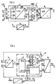
- the basic circuit diagram shown in FIG. 1 contains a clock regenerator 2, to which a synchronous multiplex signal MS is fed via input 1.
- the output of the clock regenerator is connected to a 'frame detection and clock supply' 3 which supplies the gap clocks TL1 to TLN assigned to the individual digital signals and the corresponding stuffing information SI1 to SIN.
- Circuits for a clock regenerator 2 and a 'frame recognition and clock supply' 3 are familiar to any person skilled in the art and are described, for example, in "Digital Transmission Technology" by Peter Kahl, Decker's Verlag, Volume 1 under 2.1.2.3.10, pages 22 to 25.
- the received multiplex signal MS is fed to the data inputs, for example the data input 61, from N buffer memories, of which only the buffer memory 6 is shown for the first data signal DS1.
- the stuffing information signals SI1 to SIN are each fed to a ramp counter 5 via an encoder 4. Its outputs 53 and 54 are via a logic circuit 7 with the control inputs 81 and 82 of a frequency divider 8 connected, the clock input E8 of the system clock TS is supplied.
- the clock output 11 of the frequency divider 8 is connected to the read clock input 64 of the buffer memory 6.
- a timer 9 supplies a memory clock signal TE derived from the system clock TS to the logic circuit 7.
- the buffer memory 6, the ramp counter 5 and the frequency divider 8 are provided separately for each digital signal.
- the encoder 4 and the timer 9 (or parts thereof) can be used in common for all digital signals.
- the system clock TS is derived in the clock regenerator 2 from the multiplex signal MS present at the input 1.
- the 'frame detection and clock supply' 3 recognizes the beginning of the frame by means of a frame password or corresponding defined bit sequences and assigns the individual digital signals, e.g. to the digital signal DS1, a corresponding gap clock, the write clock TL1, with which the digital signal DS1 is written into the buffer memory 6.
- the task of the ramp counter 5, the timer 9 and the frequency divider 8 is to generate an output clock TA1 which is as uniform as possible, with which the digital signal TS1 is read out from the buffer memory 6 and is output at the data output 62 of the memory or at the digital signal output 10, while the associated clock signal TA1 is present at the clock output 11.
- the data rate of the digital signal received and the digital signal read out must match.
- the output clock signal TA1 is not controlled by the filling level of the buffer memory but only by the stuffing information SI1 (if one disregards interference on the transmission path and the switch-on phase).
- the frequency divider 8 allows the aperiodic quasi-periodic frequency synthesis or frequency division, as described in the magazine Frequency 27, (1973) 9, pages 249 to 254 and Frequency 27 (1973) 10, pages 279 to 283. It consists of a first switchable A / B divider 86, the clock input E8 of which is supplied with the system clock signal TS and which outputs the output clock signal TA1 at the clock output 11.
- This divider is followed by a further C divider 87 which counts the subperiods and whose counter reading ZC specifies the current subperiod - A or B - of the A / B divider 86 and control signals SAP and SEP for determining the next subperiod via a decoder 88.
- the outputs of the decoder are routed to synchronization inputs 83 and 84 of a synchronization circuit 89. This is fed via the control inputs 81 and 82 phase correction commands EB and AB.
- the control output A89 leads to the control input of the C-divider 87.
- the frequency of the system clock is 129.6 MHz and the clock frequency of the output clock TA is 2.048 MHz.
- a suitable subperiod distribution for this is: BAAA BAA BAAA BAA BAAA BAA BAAA BAA BAAA BAA BAAA BAAA BAAA BAAA After each sub-period A or B, a pulse of the output clock signal TA1 is output, with which the digital signal DS1 is read out. These pulses of the output clock signal and the steps (bits) of the digital signal have a minimal jitter due to the frequency division, which need not be further reduced.
- a sub-period A or B is faded in or out via the synchronizing circuit by means of the synchronizing signal SY which intervenes in the C-divider.
- the fading in or out of a sub-period can take place at the same time intervals defined by the timer 9, which correspond to a normal over-period with 32 sub-periods. If this happens to be an unsuitable B sub-period, the next A sub-period is shown or hidden.
- the timer 9 can also be replaced by the dividers 86, 87 and the decoder 88.
- a modified store-in clock signal TEC is generated, the clocks of which have slightly different distances when fading in and out, but always occur at the same position of an overperiod - as in the following example - and via the dashed connection from the decoder to the synchronization circuit 89.
- a correction step should be carried out in every line. This is explained in more detail in the following Table 1. For example, a short A sub-period should be shown; this is sub-period A.
- the first line a00) shows the regular over-period of the frequency divider 8.
- an A sub-period z. B. in the sixth position there is an extended over-period a01), which has a short A-sub-period more, ie the average duration of the sub-period decreases slightly.
- the period pattern shifts to the right after each insertion of an A subperiod from the inserted A subperiod.
- the next line b01) in the table shows only the 32 sub-periods that belong to one over-period.
- the last A sub-period identified by a preceding space becomes the first sub-period of the next over-period b02) with 32 sub-periods.
- Some of the resulting over-periods are shown in Table 1, based on the original time frame.
- the original over-period is restored.
- a total of 9 B subperiods were replaced by 9 A subperiods and as a result the phase was corrected by 9 periods of the system clock signal (overperiod b00) without correction counted in).
- N 225 of these A sub-periods must be faded in in order to achieve a phase correction by one UI overall.
- the circuits for the A / B divider 86, the C divider 87 and the decoder 88 can be implemented in various ways by a person skilled in the art. It is also sufficient to feed back a line for controlling the A or B period if the correct times for switching between the periods are realized in the A / B divider 86 itself.
- Periods are faded in and faded out via control inputs 81 and 82.
- An 'insert command' EB causes a further A period to be faded in at a suitable point determined by decoder 88 and synchronization circuit 89 by fading out one of C divider 87 supplied clock (or a switchover of the period) by a corresponding synchronization command SY.
- a 'hide command' AB causes an additional pulse so that the C counter reaches its end position faster, so it only requires C-1 counting cycles.
- FIG. 1 An exemplary embodiment of the ramp generator 5 is shown in FIG.
- This contains a logic unit LE5, which may include the encoder 4, and an up-down counter VR5 with a counting range of +/- Zm.
- the logic unit LE5 is used to set the up-down counter VR5, at its output 53 a counter reading> 0 and at its output 54 a counter reading ⁇ 0.
- the frequency divider 8 is controlled, ie an A period (or B period) is faded in at the times at which a memory pulse TE is emitted by the timer 9 or is hidden.
- the function description is based on the counter reading zero of the up-down counter VR5, i.e. the frequency divider 8 works with its target division ratio (in the example 2025/32).
- the insert command EB is fed back via the logic unit LE 5 and causes the up-down counter to be counted down by 1. This process is repeated 224 more times until the numerical value corresponding to the phase shift of 1 bit has been processed and the zero position has been reached again .
- the numerical value 225 is added to the current counter reading in the logic unit LE5.
- a corresponding negative numerical value - N is entered into the counter and added to the counter reading and - in this example - a correspondingly large number of A periods are faded out, which have an effect on the output 85 of the frequency divider 8 as minimal negative phase jumps .
- a first OR gate OR1 can be used, or if the memory is empty, a second OR gate OR2 can be used by appropriate phase correction signals + SF and -SF, ie by entering a numerical value or several numerical values, an additional phase correction of the output clock TA and thus a normalization of the degree of filling.
- Some systems work with a variable number of stuff bits or stuff bytes. This only means that the input number value N is increased accordingly if more than one bit has to be corrected. If a new stuffing command is pending before the old stuffing command has been processed, the new numerical value N (or -N) to be stored is added or subtracted to the counter reading Z and the counter is loaded again with the result.
- This control loop always works with the correction speed specified by the timer 9.
- this can also be made variable by making the period of the store cycle TE dependent on the size of the stuffing criterion. Numerous circuit variants are again conceivable for this.
- FIG. 4 shows one possibility for realizing different phase correction speeds.
- the logic circuit 7 * connected between the ramp generator 5 and the frequency divider 8 contains a so-called segment 71, at whose outputs two distributor circuits 72 and 73 are connected.
- the timer 9 * delivers four different pulse sequences with the same phase spacing.
- the segment 71 now switches through one, two or four store cycles TE1 ... TE4 during a period of the timer 9 *, as a result of which the fade-in or fade-out during a period Sub-periods are possible several times.
- memory pulses with a correspondingly higher pulse repetition frequency (this corresponds to the combination of the pulses TE1 to TE4 via an OR circuit) are transmitted to the individual distributor circuits and the pulse trains are generated with frequency pulse frequencies that are sometimes lower by frequency dividers.
- the segment 71 can also be part of the synchronization circuit 89 in FIG. 2, to which the counter reading Z of the ramp counter is then also supplied via a further control input E89.
Abstract
Description
Um plesiochrone Digitalsignale in einem Datenkanal mit konstanter Bitrate übertragen zu können, erfolgt eine Anpassung der Bitraten durch Stopfen. Das übertragene Signal enthält das Datensignal und in periodischen Anständen Stopfstellen, die je nach Bedarf entweder Bits des Datensignals oder Leerbits enthalten.
Wenn die Bitrate des Datensignals hinter der reservierten Übertragungsbitrate zurückbleibt, müssen Leerbits eingefügt werden; dies wird als Positiv-Stopfen bezeichnet.In order to be able to transmit plesiochronous digital signals in a data channel with a constant bit rate, the bit rates are adjusted by stuffing. The transmitted signal contains the data signal and, at regular intervals, justification points, which contain either bits of the data signal or empty bits as required.
If the bit rate of the data signal remains behind the reserved transmission bit rate, empty bits must be inserted; this is called positive plug.
Überschreitet dagegen die Bitrate des Datensignals die reservierte Übertragungsbitrate, dann wird zusätzlich mindestens ein Datenbit in die Stopfstelle(n) eingefügt; dies wird als Negativ-Stopfen bezeichnet.
Stopfverfahren, die beide Stopfarten nutzen, werden als Positiv-Null-Negativ-Stopfverfahren bezeichnet.
Diese Verfahren werden auch dann angewendet, wenn mehrere Digitalsignale zu einem Multiplexsignal zusammengefügt werden oder wenn Multiplexsignale einer unteren Hierarchieebene zu einem Multiplexsignal einer höheren Hierarchieebene zusammengefaßt werden, wie dies beispielsweise bei den gebräuchlichen PCM-Multiplexverfahren oder bei der synchronen digitalen Hierarchie (SDH) erfolgt.If, on the other hand, the bit rate of the data signal exceeds the reserved transmission bit rate, then at least one data bit is additionally inserted into the justification point (s); this is called a negative plug.
Tamping processes that use both types of tamping are referred to as positive-zero-negative tamping processes.
These processes are applied even when multiple digital signals are combined into a multiplex signal, or if multiplex signals are combined a lower hierarchy level to a multiplex signal of a higher hierarchical level, as for example in the usual PCM multiplexing method or the s ynchronen d igitalen H ierarchie (SDH ) he follows.
Die Stopfvorgange umfassen jeweils ein Bit oder mehrere Bits oder auch ein oder mehrere Bytes.
Jeder Stopfvorgang erzeugt einen Phasensprung des abgehenden Digitalsignals. Auf der Empfangsseite wird das Digitalsignal mit einem Lückentaktsignal in einen Pufferspeicher eingeschrieben und mit einem kontinuierlichen Taktsignal ausgelesen. Die Phasensprünge des Digitalsignals bzw. des zugehörigen Ausgabetaktsignals werden am Empfangsort durch eine analoge oder digitale Phasenregelschleife (PLL) geglättet. Entsprechend ihrer Dimensionierung wirkt die Phasenregelschleife wie ein Tiefpaß. Die Amplitude der durch Stopfen verursachten Phasensprünge (Jitter) wird durch die Phasenregelschleife stark reduziert, falls der zeitliche Abstand der Phasensprünge sehr klein gegenüber der Zeitkonstante der Phasenregelschleife ist.The stuffing operations each include one bit or more bits or one or more bytes.
Each tamping process creates a phase jump in the outgoing digital signal. The digital signal is on the receiving side written into a buffer memory with a gap clock signal and read out with a continuous clock signal. The phase jumps of the digital signal or the associated output clock signal are smoothed at the receiving location by an analog or digital phase locked loop (PLL). Depending on its dimensions, the phase-locked loop acts like a low-pass filter. The amplitude of the phase jumps (jitter) caused by plugging is greatly reduced by the phase-locked loop if the time interval between the phase jumps is very small compared to the time constant of the phase-locked loop.
Beim Positiv-Null-Negativ-Stopfverfahren können die zeitlichen Abstände der Phasensprünge jedoch sehr groß sein. In diesem Fall werden ohne zusätzliche Maßnahmen die Phasensprünge durch die Phasenregelschleife wenig gedämpft. Aus der internationalen Patentanmeldung WO 91/12678 ist ein Verfahren und eine Anordnung zur Taktrückgewinnung bekannt. Sprunghafte Änderung der Korrekturgröße für die Regelschleife werden zunächst unterdrückt, um sie dann innerhalb einer längeren Ausgleichszeit kontinuierlich oder in kleinen Schritten an eine digital ausgeführte Phasenregelschleife weiterzugeben.
Die Steuerung der Phasenregelschleife erfolgt abhängig vom Füllstand eines Rampenzählers, in den Anfangswerte bei Stopfvorgängen geladen werden. Nur in der Endstellung des Rampenzählers erfolgt eine Steuerung eines PLL-Zählers, der die Frequenz des Ausgabetaktes bestimmt, durch den Füllstand des Pufferspeichers. Die Regelschleife ist so konzipiert, daß auch bei einem synchronen Taktsignal ständig eine Phasenkorrektur erfolgt. Zur Realisierung werden zahlreiche Zähler und eine relativ komplizierte Aritbmetik benötigt.
Hierdurch erfolgt nur eine langsame Änderung der Phase des Taktsignals.With the positive-zero-negative stuffing method, the time intervals of the phase jumps can be very large. In this case, the phase jumps are damped little by the phase locked loop without additional measures. A method and an arrangement for clock recovery are known from international patent application WO 91/12678. Abrupt changes in the correction variable for the control loop are initially suppressed, in order to then pass them on continuously or in small steps to a digitally executed phase control loop within a longer compensation time.
The phase locked loop is controlled depending on the fill level of a ramp counter, in which the initial values are loaded during tamping processes. Only in the end position of the ramp counter is a PLL counter, which determines the frequency of the output clock, controlled by the fill level of the buffer memory. The control loop is designed in such a way that a phase correction is carried out continuously even with a synchronous clock signal. Numerous counters and a relatively complicated arithmetic are required for implementation.
As a result, there is only a slow change in the phase of the clock signal.
Durch die geringe Geschwindigkeit der Phasenkorrektur wird aus einem sonst erzeugten Jitter eine als Wander bezeichnete allmählichen Änderung der Phase.Due to the low speed of the phase correction, an otherwise generated jitter becomes a gradual change in the phase, known as wander.
Aufgabe der Erfindung ist es, eine einfachere digital arbeitende Anordnung für den Empfangsteil anzugeben, die nur einen minimalen Jitter mit hoher Frequenz erzeugt. Diese sollte einfach an die unterschiedlichen Datenraten angepaßt werden können.The object of the invention is to provide a simpler digitally working arrangement for the receiving part, which generates only a minimal jitter with a high frequency. It should be easy to adapt to the different data rates.
Diese Aufgabe wird durch die im Anspruch 1 angegebene Anordnung zur Rückgewinnung eines Digitalsignals gelöst.This object is achieved by the arrangement for recovering a digital signal.
Vorteilhafte Ausbildungen sind in den Unteransprüchen angegeben.Advantageous designs are specified in the subclaims.
Besonders vorteilhaft bei der Anordnung ist, daß die Steuerung der Phasenkorrektur nur durch die Stopfinformation erfolgt und nicht wie bisher vom Speicherinhalt abhängig gemacht wird. Lediglich in der Einschaltphase und bei Störungen wird der Füllgrad des Speichers ebenfalls als Steuerkriterium zur Phasenkorrektur verwendet.
Ein Hilfsoszillator ist bei dieser Anordnung nicht erforderlich.It is particularly advantageous in the arrangement that the phase correction is controlled only by the stuffing information and is not made dependent on the memory content as before. The fill level of the memory is also used as a control criterion for phase correction only in the switch-on phase and in the event of faults.
An auxiliary oscillator is not required with this arrangement.
Besonders vorteilhaft ist die Verwendung eines aperiodischquasiperiodischen Teilers, durch den sich alle rationalen Teilungsverhältnisse realisieren lassen. Durch Einfügen oder Ausblenden von Unterperioden dieses Teilers wird nur ein minimaler Jitter bewirkt.It is particularly advantageous to use an aperiodic-quasi-periodic divider, by means of which all rational division ratios can be realized. By inserting or hiding sub-periods of this divider, there is only minimal jitter.
Zweckmäßig ist die Verwendung eines Rampengenerators zur Steuerung der Stopfvorgänge. Bei jedem Stopfvorgang wird ein Zahlenwert geladen, der in zahlreichen Phasenkorrekturen wieder auf seinen Nullwert reduziert wird.It is advisable to use a ramp generator to control the tamping processes. A numerical value is loaded with each tamping process, which is reduced to its zero value in numerous phase corrections.
Die Geschwindigkeit der Phasenkorrektur kann auch von der Größe und der Häufigkeit der erforderlichen durch die Stopfinformation vorgegebene Phasenkorrektur abhängig erfolgen.
Einer der größten Vorteile der Erfindung besteht in der Verwendung von programmierbaren Teilern. Hierdurch ist die Anordnung an die unterschiedlichsten Datenraten und an alle Erfordernisse bei den Stopfvorgängen anpaßbar.The speed of the phase correction can also depend on the size and the frequency of the required phase correction specified by the stuffing information.
One of the greatest advantages of the invention is the use of programmable dividers. This is the arrangement adaptable to the most varied data rates and to all requirements for the tamping processes.
Die Erfindung wird anhand von Figuren näher erläutert.
Es zeigen:
- Fig. 1
- ein Prinzipschaltbild der Anordnung,
- Fig. 2
- ein Blockschaltbild eines steuerbaren A/B-Frequenzteilers,
- Fig. 3
- ein Blockschaltbild eines Rampengenerators und
- Fig. 4
- eine Variante des Rampengenerators für unterschiedliche Zeitkonstanten.
Show it:
- Fig. 1
- a schematic diagram of the arrangement,
- Fig. 2
- a block diagram of a controllable A / B frequency divider,
- Fig. 3
- a block diagram of a ramp generator and
- Fig. 4
- a variant of the ramp generator for different time constants.
Das in Figur 1 dargestellte Prinzipschaltbild enthält einen Taktregenerator 2, dem über den Eingang 1 ein synchrones Multiplexsignal MS zugeführt wird. Der Ausgang des Taktregenerators ist mit einer 'Rahmenerkennung und Taktversorgung' 3 verbunden, die den einzelnen Digitalsignalen zugeordnete Lückentakte TL1 bis TLN und die entsprechende Stopfinformation SI1 bis SIN liefert. Schaltungen für einen Taktregenerator 2 und eine 'Rahmenerkennung und Taktversorgung' 3 sind jedem Fachmann geläufig und beispielsweise in "Digitale Übertragungstechnik" von Peter Kahl, Decker's Verlag, Band 1 unter 2.1.2.3.10, Seite 22 bis 25 beschrieben.The basic circuit diagram shown in FIG. 1 contains a
Das empfangene Multiplexsignal MS wird den Dateneingängen, z.B. dem Dateneingang 61, von N Pufferspeichern zugeführt, von denen nur der Pufferspeicher 6 für das erste Datensignal DS1 dargestellt ist. Ein Ausgang der 'Rahmenerkennung und Taktversorgung' 3 , an dem ein Lücken aufweisender Schreibtakt abgegeben wird, ist mit einem Schreibtakt-Eingang 63 des Pufferspeichers verbunden. Von der 'Rahmenerkennung und der Taktversorgung' 3 werden die Stopfinformationssignale SI1 bis SIN über einen Codierer 4 jeweils einem Rampenzähler 5 zugeführt. Dessen Ausgänge 53 und 54 sind über eine Logikschaltung 7 mit den Steuereingängen 81 bzw. 82 eines Frequenzteilers 8 verbunden, dessen Takteingang E8 der Systemtakt TS zugeführt ist.The received multiplex signal MS is fed to the data inputs, for example the
Der Taktausgang 11 des Frequenzteilers 8 ist mit dem Lesetakt-Eingang 64 des Pufferspeichers 6 verbunden. Ein Zeitgeber 9 liefert ein vom Systemtakt TS abgeleitetes Speichertaktsignal TE an die Logikschaltung 7.
Der Pufferspeicher 6, der Rampenzähler 5 und der Frequenzteiler 8 sind für jedes Digitalsignal seperat vorgesehen. Der Codierer 4 und der Zeitgeber 9 (oder Teile von diesen) können gemeinsam für alle Digitalsignale genutzt werden.The
The
Von dem am Eingang 1 anliegenden Multiplexsignal MS wird in dem Taktregenerator 2 der Systemtakt TS abgeleitet. Die 'Rahmenerkennung und Taktversorgung' 3 erkennt durch ein Rahmenkennwort oder entsprechende festgelegte Bitfolgen den Rahmenanfang und ordnet den einzelnen Digitalsignalen, z.B. dem Digitalsignal DS1, einen entsprechenden Lückentakt, den Schreibtakt TL1 zu, mit dem das Digitalsignal DS1 in den Pufferspeicher 6 eingeschrieben wird.The system clock TS is derived in the
Die Aufgabe des Rampenzählers 5, des Zeitgebers 9 und des Frequenzteilers 8 besteht darin, einen möglichst gleichmäßigen Ausgabetakt TA1 zu erzeugen, mit dem das Digitalsignal TS1 aus dem Pufferspeicher 6 ausgelesen und am Datenausgang 62 des Speicher bzw. am Digitalsignal-Ausgang 10 abgegeben wird, während das zugehörige Taktsignal TA1 am Taktausgang 11 anliegt.
Im Mittel muß die Datenrate des empfangenen Digitalsignals und des ausgelesenen Digitalsignals übereinstimmen.The task of the
On average, the data rate of the digital signal received and the digital signal read out must match.
Im Gegensatz zu den bekannten Schaltungen zur Taktanpassung auf der Empfangsseite wird das Ausgabetaktsignal TA1 nicht vom Füllgrad des Pufferspeichers sondern nur von der Stopfinformation SI1 gesteuert (wenn man von Störungen auf dem Übertragungsweg und der Einschaltphase absieht).In contrast to the known circuits for clock adaptation on the receiving side, the output clock signal TA1 is not controlled by the filling level of the buffer memory but only by the stuffing information SI1 (if one disregards interference on the transmission path and the switch-on phase).
Zunächst soll die Funktion des in FIGUR 2 genauer dargestellten Frequenzteilers 8 näher erläutert werden. Der Frequenzteiler 8 gestattet die aperiodisch quasiperiodische Frequenzsynthese bzw. Frequenzteilung, wie sie in der Zeitschrift Frequenz 27, (1973) 9, Seite 249 bis 254 und Frequenz 27 (1973) 10, Seite 279 bis 283 beschrieben ist. Er besteht aus einem ersten umschaltbaren A/B-Teiler 86, dessen Takteingang E8 das Systemtaktsignal TS zugeführt wird und der am Taktausgang 11 das Ausgabetaktsignal TA1 abgibt. Diesem Teiler ist ein weiterer C-Teiler 87 nachgeschaltet, der die Unterperioden zählt und dessen Zählerstand ZC über einen Decoder 88 die aktuelle Unterperiode - A oder B -des A/B-Teilers 86 und Steuersignale SAP und SEP zur Festlegung der nächsten Unterperiode angibt.First, the function of the
Die Ausgänge des Decoders sind an Synchronisiereingänge 83 und 84 einer Synchronisierschaltung 89 geführt. Dieser werden über die Steuereingänge 81 und 82 Phasenkorrekturbefehle EB und AB zugeführt. Der Steuerausgang A89 ist auf den Steuereingang des C-Teilers 87 geführt.The outputs of the decoder are routed to
Mit Hilfe dieser Teileranordnung kann zunächst jedes rationale Teilungsverhältnis realisiert werden.With the help of this divider arrangement, every rational division ratio can be realized first.
Die Frequenz des Systemtaktes beträgt 129,6 MHz und die Taktfrequenz des Ausgabetaktes TA beträgt 2,048 MHz. Dies ergibt ein Teilungsverhältnis von
Mit einem A/B-Teiler 86, der die Unterperiode A = 63 und die Unterperiode B = 64 erzeugen kann, und einem C-Teiler, der einen Zählumfang von 32 A- und B-Unterperioden aufweist, kann mit n = 23 A-Unterperioden und m = 9 B-Unterperioden dieses Teilungsverhältnis realisiert werden.The frequency of the system clock is 129.6 MHz and the clock frequency of the output clock TA is 2.048 MHz. This gives a division ratio of
With an A /
Eine geeignete Unterperiodenverteilung hierzu ist:
BAAA BAA BAAA BAA BAAA BAA BAAA BAA BAAA
Nach jeder Unterperiode A oder B wird ein Impuls des Ausgabetaktsignals TA1 abgegeben, mit dem das Digitalsignal DS1 ausgelesen wird. Diese Impulse des Ausgabetaktsignals und die Schritte (Bits) des Digitalsignals weisen einen durch die Frequenzteilung bedingten minimalen Jitter auf, der nicht weiter reduziert zu werden braucht.A suitable subperiod distribution for this is:
BAAA BAA BAAA BAA BAAA BAA BAAA BAA BAAA
After each sub-period A or B, a pulse of the output clock signal TA1 is output, with which the digital signal DS1 is read out. These pulses of the output clock signal and the steps (bits) of the digital signal have a minimal jitter due to the frequency division, which need not be further reduced.
Dieses exakte Teilungsverhältnis macht Stopfvorgänge dann überflüssig, wenn synchrone Digitalsignale übertragen werden.
Da es sich hier in der Regel jedoch um plesiochrone Signale handelt, muß die Phase des A/B-Teilers verstellt werden. Bei den bisherigen Lösungen geschieht dies durch Ein- oder Ausblenden eines oder mehrerer Impulse des Eingangstaktsignals (Systemtaktsignals TS), so daß der Frequenzteiler eine kürzere oder längere Periodendauer aufweist.This exact division ratio makes stuffing operations superfluous when synchronous digital signals are transmitted.
However, since these are usually plesiochronous signals, the phase of the A / B divider must be adjusted. In the previous solutions, this is done by showing or hiding one or more pulses of the input clock signal (system clock signal TS), so that the frequency divider has a shorter or longer period.
Um den Jitter weiter zu verringern, wird hier eine andere Korrekturmethode gewählt. Über die Synchronisierschaltung wird durch in den C-Teiler eingreifendes Synchronisiersignal SY eine Unterperiode A oder B ein- oder ausgeblendet.In order to further reduce the jitter, another correction method is chosen here. A sub-period A or B is faded in or out via the synchronizing circuit by means of the synchronizing signal SY which intervenes in the C-divider.
Das Einblenden oder Ausblenden einer Unterperiode kann in gleichen, durch den Zeitgeber 9 festgelegten Zeitabständen erfolgen, die einer normalen Überperiode mit 32 Unterperioden entsprechen. Ist dies zufällig eine ungeeignete B-Unterperiode wird die nächste A-Unterperiode ein- oder ausgeblendet.
Der Zeitgeber 9 kann auch durch die Teiler 86, 87 und den Decoder 88 ersetzt werden. Es wird ein modifiziertes Einspeichertaktsignal TEC erzeugt, dessen Takte zwar beim Ein- und Ausblenden geringfügig unterschiedliche Abstände aufweisen, dafür jedoch stets an derselben Position einer Überperiode auftreten - wie im folgenden Beispiel - und über die strichlierte Verbindung von Decoder zur Synchronisierschaltung 89 gelangen.The fading in or out of a sub-period can take place at the same time intervals defined by the timer 9, which correspond to a normal over-period with 32 sub-periods. If this happens to be an unsuitable B sub-period, the next A sub-period is shown or hidden.
The timer 9 can also be replaced by the
Bei den geringen Frequenzunterschieden erfolgen Korrekturvorgänge in größeren Zeitabständen. In dem foldenden Beispiel, das lediglich zur Ermittlung der Größe eines Korrekturschrittes dient, soll dagegen in jeder Zeile ein Korrekturschritt erfolgen. Dies wird anhand der folgenden Tabelle 1 näher erläutert.Beispielsweise soll eine kurze A-Unterperiode eingeblendet werden; dies ist die Unterperiode A .

Die erste Zeile a00) zeigt die reguläre Überperiode des Frequenzteilers 8.
Durch das Einfügen einer A -Unterperiode z. B. in der sechsten Position ergibt sich eine verlängerte Überperiode a01), die eine kurze A-Unterperiode mehr aufweist, d. h. die durchschnittliche Unterperiodendauer verkleinert sich geringfügig.The first line a00) shows the regular over-period of the
By inserting an A sub-period z. B. in the sixth position there is an extended over-period a01), which has a short A-sub-period more, ie the average duration of the sub-period decreases slightly.
Bezogen auf die ursprünliche Überperiodendauer verschiebt sich ab der eingefügten A -Unterperiode das Periodenmuster nach jeder Einfügung einer A-Unterperiode nach rechts. Die nächste Zeile b01) in der Tabelle zeigt nur die 32 Unterperioden, die zu einer Überperiode gehören. Die letzte durch einen vorausgehenden Zwischenraum gekennzeichnete A-Unterperiode wird die erste Unterperiode der nächsten Überperiode b02) mit 32 Unterperioden. Um die Phase des Ausgangstaktes um ein zusätzlich eingefügtes Stopfbit korrigieren zu können, sind viele dieser Korrekturschritte notwendig. Einige der hieraus resultierenden Überperioden sind - bezogen auf den ursprünglichen Zeitrahmen - in der Tabelle 1 dargestellt.Based on the original overperiod, the period pattern shifts to the right after each insertion of an A subperiod from the inserted A subperiod. The next line b01) in the table shows only the 32 sub-periods that belong to one over-period. The last A sub-period identified by a preceding space becomes the first sub-period of the next over-period b02) with 32 sub-periods. In order to be able to correct the phase of the output clock by an additional stuff bit, many of these correction steps are necessary. Some of the resulting over-periods are shown in Table 1, based on the original time frame.
Nach 32 Korrekturschritten ist die ursprüngliche Überperiode wieder hergestellt. Während der 32 Korrekturschritte (d. h. in der Tabelle nach 32 aufeinanderfolgenden Überperioden mit jeweils 32 Unterperioden) wurden insgesamt 9 B-Unterperioden durch 9 A-Unterperioden erstetzt und hierdurch wurde die Phase um 9 Perioden des Sytemtaktsignals korrigiert (Die Überperiode b00) ohne Korrektur wurde nicht mitgezählt).
Die so erzielte Phasenkorrektur beträgt im Mittel je Korrekturschritt (je eingefügter A-Periode):
(mit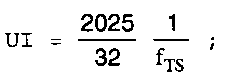
UI = Bitdauer des ausgegebenen Digitalsignals von 2,048 Mbit/s).After 32 correction steps, the original over-period is restored. During the 32 correction steps (i.e. in the table after 32 consecutive overperiods with 32 subperiods each) a total of 9 B subperiods were replaced by 9 A subperiods and as a result the phase was corrected by 9 periods of the system clock signal (overperiod b00) without correction counted in).
The phase correction achieved in this way is on average per correction step (per inserted A period):
(With
UI = bit duration of the output digital signal of 2.048 Mbit / s).
Es müssen folglich N = 225 dieser A-Unterperioden eingeblendet werden, um insgesamt eine Phasenkorrektur von einem UI zu erreichen.Consequently, N = 225 of these A sub-periods must be faded in in order to achieve a phase correction by one UI overall.
Mit dem Einfügen (oder Ausblenden)von Unterperioden wird somit eine äußerst feine Phaseneinstellung des Arbeitstaktes möglich, wobei die Jitterfrequenz praktisch nicht verändert wird und eine Phasenkorrektur nur Bruchteile einer Periode des Systemtaktsignals TS ausmacht.With the insertion (or fading out) of sub-periods, an extremely fine phase adjustment of the operating cycle is possible, the jitter frequency being practically unchanged and a phase correction making up only a fraction of a period of the system clock signal TS.
Die Schaltungen für den A/B-Teiler 86, den C-Teiler 87 und den Decoder 88 können auf unterschiedlichste Weise vom Fachmann realisiert werden. Es ist auch ausreichend, eine Leitung zur Steuerung der A- oder B-Periode rückzukoppeln, wenn die korrekten Zeitpunkte zum Umschalten zwischen den Perioden im A/B-Teiler 86 selbst realisiert werden.The circuits for the A /
Das Ein- und Ausblenden von Perioden erfolgt über die Steuereingänge 81 und 82. Ein 'Einfügen-Befehl' EB bewirkt an geeigneter durch den Decoder 88 und die Synchronisierschaltung 89 festgelegter Stelle das Einblenden einer weiteren A-Periode durch Ausblenden eines dem C-Teiler 87 zugeführten Taktes (oder einer Umschaltung der Periodendauer) durch einen entsprechenden Synchronisierbefehl SY. Ein 'Ausblenden-Befehl' AB bewirkt dagegen einen Zusatzimpuls, so daß der C-Zähler schneller seine Endstellung erreicht, also nur C-1 Zähltakte benötigt.Periods are faded in and faded out via
In Figur 3 ist ein Ausführungsbeispiel des Rampengenerators 5 dargestellt. Dieser enthält eine Logikeinheit LE5, die gegebenenfalls den Codierer 4 beinhaltet, und einen Vorwärts-Rückwärts-Zähler VR5 mit einem Zählbereich von +/- Zm. Der Logikeinheit wird entweder die Stopfinformation SI zugeführt, die sie dann in einen Zahlenwert umsetzt, oder bereits der entsprechende Zahlenwert zugeführt, in diesem Beispiel +N (= +225) oder -N , der die Anzahl der durchzuführenden Korrekturvorgänge (der ein- oder auszublendenden A-Perioden) beinhaltet. Die Logikeinheit LE5 dient zum Einstellen des Vorwärts-Rückwärts-Zählers VR5, an dessen Ausgang 53 ein Zählerstand >0 und an dessen Ausgang 54 ein Zählerstand <0 abgegeben wird. Über die Logikschaltung 7, die hier zwei UND-Gatter N1 und N2 enthält, wird zu den Zeitpunkten, an denen jeweils vom Zeitgeber 9 ein Einspeicherimpuls TE abgegeben wird, der Frequenzteiler 8 angesteuert, d.h. eine A-Periode (oder B-Periode) eingeblendet oder ausgeblendet wird.An exemplary embodiment of the
Zur Funktionsbeschreibung wird von dem Zählerstand Null des Vorwärts-Rückwärts-Zählers VR5 ausgegangen , d.h. der Frequenzteiler 8 arbeitet mit seinem Sollteilungsverhältnis (im Beispiel 2025/32).The function description is based on the counter reading zero of the up-down counter VR5, i.e. the
Soll eine Phasenkorrektur um ein Bit erfolgen, so muß ein bestimmter Zahlenwert +N = 225 in den Vorwärts-Rückwärts-Zähler VR5 geladen werden. Hierdurch wird der Zählerstand Z > 0 und somit das erste UND-Gatter AND1 zum Zeitpunkt des Einspeicherimpulses TE freigegeben. Folglich wird dem Frequenzteiler 8 ein erster Einfügen-Befehl EB zugeführt, der - in diesem Beispiel - eine A-Periode einfügt. Hierdurch ergibt sich am Taktausgang 85 ein minimaler positiver Phasensprung.
Der Einfügen-Befehl EB wird über die Logik-Einheit LE 5 zurückgekoppelt und bewirkt das Rückwärtszählen des Vorwärts-Rückwärts-Zählers um 1. Dieser Vorgang wiederholt sich noch 224mal bis der dem Phasensprung von 1 Bit entsprechende Zahlenwert abgearbeitet ist und die Nullstellung wieder erreicht ist.If a phase correction by one bit is to be carried out, a specific numerical value + N = 225 must be loaded into the up-down counter VR5. This releases the counter reading Z> 0 and thus the first AND gate AND1 at the time of the store pulse TE. Consequently, the
The insert command EB is fed back via the
Ist dagegen der Zählerstand bei einen anliegende Einblenden Befehl ungleich Null, dann wird der Zahlenwert 225 zu dem aktuellen Zählerstand in der Logikeinheit LE5 hinzuaddiert.
Bei einem entgegengesetzt gerichteten Ausblenden-Befehl AB wird ein entsprechender negativer Zahlenwert - N in den Zähler eingegebenund zum Zählerstand addiert und es werden - in diesem Beispiel - entsprechend viele A-Perioden ausgeblendet, die sich am Ausgang 85 des Frequenzteilers 8 als minimale negative Phasensprünge auswirken.If, on the other hand, the counter reading is not zero when a fade-in command is present, then the numerical value 225 is added to the current counter reading in the logic unit LE5.
In the case of an oppositely directed fade-out command AB, a corresponding negative numerical value - N is entered into the counter and added to the counter reading and - in this example - a correspondingly large number of A periods are faded out, which have an effect on the output 85 of the
Im 'eingeschwungenen' Zustand der Anordnung muß eine Überwachung des Speicherinhalts nicht mehr erfolgen. Während der Einschaltphase und bei Übertragungsfehlern der Stopfinformation usw. kann es jedoch zu einer Fehlsteuerung bei der Speicherbelegung kommen. Bei einem zu vollen Speicher kann daher über ein erstes OR-Gatter OR1 oder bei zu leeren Speicher über ein zweites OR-Gatter OR2 durch entsprechende Phasenkorrektursignale +SF und -SF , also durch Eingabe eines Zahlenwertes oder mehrerer Zahlenwerte, eine zusätzliche Phasenkorrektur des Ausgabetaktes TA und damit eine Normalisierung des Füllgrades erfolgen.In the 'steady' state of the arrangement, the memory content no longer has to be monitored. During the switch-on phase and in the event of transmission errors in the stuffing information etc., incorrect control of the memory allocation can occur. If the memory is too full, a first OR gate OR1 can be used, or if the memory is empty, a second OR gate OR2 can be used by appropriate phase correction signals + SF and -SF, ie by entering a numerical value or several numerical values, an additional phase correction of the output clock TA and thus a normalization of the degree of filling.
Bei einigen Systemen wird mit einer variablen Anzahl von Stopfbits oder Stopfbytes gearbeitet. Dies bedeutet lediglich, daß der Eingangszahlenwert N entsprechend heraufgesetzt wird, wenn um mehr als ein Bit korrigiert werden muß. Wenn ein neuer Stopfbefehl anliegt, bevor der alte Stopfbefehl abgearbeitet ist, dann wird zu dem Zählerstand Z der neue einzuspeichernde Zahlenwert N (oder -N) addiert bzw. subtrahiert und der Zähler mit dem Ergebnis erneut geladen.Some systems work with a variable number of stuff bits or stuff bytes. This only means that the input number value N is increased accordingly if more than one bit has to be corrected. If a new stuffing command is pending before the old stuffing command has been processed, the new numerical value N (or -N) to be stored is added or subtracted to the counter reading Z and the counter is loaded again with the result.
Diese Regelschleife arbeitet stets mit der vom Zeitgeber 9 vorgegebenen Korrekturgeschwindigkeit. Diese kann natürlich auch variabel gestaltet werden, indem die Periodendauer des Einspeichertaktes TE von der Größe des Stopfkriteriums abhängig gemacht wird. Hierzu sind wieder zahlreiche Schaltungsvarianten denkbar.This control loop always works with the correction speed specified by the timer 9. Of course, this can also be made variable by making the period of the store cycle TE dependent on the size of the stuffing criterion. Numerous circuit variants are again conceivable for this.
In Figur 4 ist eine Möglichkeit zur Realisierung unterschiedlicher Phasenkorrekturgeschwindigkeiten dargestellt.
Die zwischen dem Rampengenerator 5 und dem Frequenzteiler 8 eingeschaltete Logikschaltung 7* enthält einen sogenannten Segmenter 71, an dessen Ausgänge zwei Verteilerschaltungen 72 bzw. 73 angeschaltet sind. Der Zeitgeber 9* liefert vier unterschiedliche Impulsfolgen mit gleichen Phasenabständen. Der Segmenter 71 schaltet nun in Abhängigkeit der aus dem Zählerstand Z des Rampenzählers 5 ermittelten Korrektursignale KS einen, zwei oder vier Einspeichertakte TE1...TE4 während einer Periode des Zeitgebers 9* durch, wodurch während einer Periode das dann Ein- bzw. Ausblenden von Unterperioden mehrmals möglich ist.
Um Verbindungsleitungen zu sparen, können Einspeicherimpulse mit entsprechend höherer Pulsfolgefrequenz (dies entspricht der Zusammenfassung der Impulse TE1 bis TE4 über eine ODER-Schaltung) zu den einzelnen Verteilerschaltungen übertragen werden und die Impulsfolgen mit teilweise niedrigeren Pulsfolgefrequenzen durch Frequenzteiler erzeugt werden.FIG. 4 shows one possibility for realizing different phase correction speeds.
The
In order to save connecting lines, memory pulses with a correspondingly higher pulse repetition frequency (this corresponds to the combination of the pulses TE1 to TE4 via an OR circuit) are transmitted to the individual distributor circuits and the pulse trains are generated with frequency pulse frequencies that are sometimes lower by frequency dividers.
Der Segmenter 71 kann auch Teil der Synchronisierschaltung 89 in Figur 2 sein, der dann auch der Zählerstand Z des Rampenzählers über einen weiteren Steuereingang E89 zugeführt wird.The segment 71 can also be part of the
Eine weitere Möglichkeit zur Realisierung einer vom Zählerstand Z abhängigen Phasenkorrekturgeschwindigkeit besteht darin, den Zählerstand Z in einen weiteren Zähler mit einer längeren Zählperiode zu laden (oder vorher von einer Konstanten zu subtrahieren), bei dessen Endstand ein Korrekturimpuls abgegeben wird, wie dies beim eingangs beschriebenen Stand der Technik der Fall ist.Another possibility for realizing a phase correction speed dependent on the counter reading Z is to load the counter reading Z into another counter with a longer counting period (or to subtract it beforehand from a constant), at the final reading of which a correction pulse is emitted, as described in the introduction State of the art is the case.
Claims (10)
mit einem empfangsseitigen Pufferspeicher (6), in den das Digitalsignal (DS1) mit einem Schreibtakt(TL1) eingeschrieben und mit einem Ausgabetakt (TA1) ausgelesen wird,
dadurch gekennzeichnet,
daß ein Rampengenerator (5; LE5, VR5) vorgesehen ist, in den ein der Größe des Stopfvorganges entsprechender Zahlenwert (z.B. +N) eingespeichert wird,
daß ein Frequenzteiler (8) zum Erzeugen des Ausgabetaktes (TA1) vorgesehen ist, an dessen Steuereingänge (81, 82) die Steuerausgänge (53, 54) des Rampengenerators (5; LE5, VR5) geführt sind, und
daß ein Zeitgeber (9, 9*) vorgesehen ist, der in vorbestimmten Zeitabständen ein Einspeichertaktsignal (TE, TEC) abgibt, das aufgrund des Zählstandes (Z) des Rampengenerators (5; LE5, VR5) eine Änderung der Überperiodendauer (BAAABAA......BAAA) des Frequenzteilers (8) steuert und gleichzeitig eine Verringerung des Zählerstandes (Z) in Richtung der Nullage des Rampengenerators (5; LE5, VR5) bewirkt.Arrangement for recovering at least one plesiochronous digital signal (DS1), which is transmitted in time slots of a synchronous signal (MS), frequency differences being compensated for by plugging,
with a buffer memory (6) on the reception side, into which the digital signal (DS1) is written with a write clock (TL1) and read out with an output clock (TA1),
characterized by
that a ramp generator (5; LE5, VR5) is provided, in which a numerical value corresponding to the size of the tamping process (for example + N) is stored,
that a frequency divider (8) is provided for generating the output clock (TA1), at whose control inputs (81, 82) the control outputs (53, 54) of the ramp generator (5; LE5, VR5) are guided, and
that a timer (9, 9 *) is provided which, at predetermined time intervals, emits a store clock signal (TE, TEC) which, due to the count (Z) of the ramp generator (5; LE5, VR5), changes the overperiod (BAAABAA ... ... BAAA) controls the frequency divider (8) and at the same time causes a reduction in the counter reading (Z) in the direction of the zero position of the ramp generator (5; LE5, VR5).
dadurch gekennzeichnet,
daß der Frequenzteiler (8) als aperiodisch-quasiperiodischer Teiler (86, 87, 88) ausgebildet ist, der mindestens zwei unterschiedliche Unterperioden (A, B) aufweist.Arrangement according to claim 1,
characterized by
that the frequency divider (8) is designed as an aperiodic-quasi-periodic divider (86, 87, 88) which has at least two different subperiods (A, B).
dadurch gekennzeichnet,
daß der Frequenzteiler (8) eine Synchronisierschaltung (89) aufweist, die durch Ein- und Ausblenden von Unterperioden (z.B. A) die Phasenkorrektur des Ausgabetaktes (TA1) steuert.Arrangement according to claim 2,
characterized by
that the frequency divider (8) has a synchronizing circuit (89) which controls the phase correction of the output clock (TA1) by showing and hiding sub-periods (eg A).
daß der Frequenzteiler (8) einen steuerbaren A/B-Teiler (86) enthält, der den Ausgabetakt (TA1) abgibt,
daß an den Ausgang des A/B-Teilers (86) ein C-Teiler (87) angeschaltet ist, der die Anzahl (C = 32) der Unterperioden (A, B) je Überperiode zählt,
daß dem C-Teiler (87) ein Decoder (88) nachgeschaltet ist, der aus dem aktuellen Zählerstand (Z) die zugehörige Unterperiode (A, B) decodert und entsprechende Steuersignale (SAP, SBP) für den A/B-Teiler (86) abgibt, und
daß die Synchronisierschaltung (89) Korrektureingänge (E83, E84) für Phasenkorrekturbefehle (EB, AB) und Steuereingänge (E81, E82), über die ihr vom Decoder (88) die aktuelle Unterperiode (A, B) signalisiert wird, aufweist, und über einen Steuerausgang (A89) die Zählperiode des C-Teilers (87) steuert.Arrangement according to claim 2 or 3,
that the frequency divider (8) contains a controllable A / B divider (86) which outputs the output clock (TA1),
that a C-divider (87) is connected to the output of the A / B divider (86) and counts the number (C = 32) of sub-periods (A, B) per over-period,
that the C-divider (87) is followed by a decoder (88) which decodes the associated sub-period (A, B) from the current counter reading (Z) and corresponding control signals (SAP, SBP) for the A / B divider (86 ) and
that the synchronization circuit (89) has correction inputs (E83, E84) for phase correction commands (EB, AB) and control inputs (E81, E82), via which the decoder (88) signals the current sub-period (A, B), and has a control output (A89) controls the counting period of the C-divider (87).
dadurch gekennzeichnet,
daß der Rampengenerator (5) einen Vorwärts-Rückwärts-Zähler (VR5) enthält, der bei Auftreten eines Stopfinformationssignals (SI1) mit einem Zahlenwert (z.B. +N) geladen wird, dessen Betrag mit jedem von ihm veranlaßten Phasenkorrekturbefehl (EB, AB) reduziert wird.Arrangement according to one of the preceding claims,
characterized by
that the ramp generator (5) contains an up-down counter (VR5) which is loaded with a numerical value (eg + N) when a stuffing information signal (SI1) occurs, the amount of which is reduced with each phase correction command (EB, AB) which it initiates becomes.
dadurch gekennzeichnet,
daß ein Zeitgeber (7) vorgesehen ist, der ein Einspeichertaktsignal (TE, TEC) abgibt, das gemeinsam mit einem Phasenkorrekturbefehl (EB, AB) Frequenzteiler (85, 86, 87) steuert.Arrangement according to one of the preceding claims,
characterized by
that a timer (7) is provided which emits a store clock signal (TE, TEC) which, together with a phase correction command (EB, AB), controls frequency dividers (85, 86, 87).
dadurch gekennzeichnet,
daß nur ein Zeitgeber (7) für mehrere Digitalsignale (DS1, ...DSn) vorgesehen ist und
daß eine Logikschaltung (7) zwischen Rampengenerator (5) und Frequenzteiler (8) eingeschaltet ist, die eine vom Zählerstand (Z) frequenzabhängige Folge von Korrekturbefehlen (EB, AB) erzeugt.Arrangement according to claim 6,
characterized by
that only one timer (7) is provided for several digital signals (DS1, ... DSn) and
that a logic circuit (7) between the ramp generator (5) and frequency divider (8) is switched on, one of the counter reading (Z) frequency-dependent sequence of correction commands (EB, AB) generated.
dadurch gekennzeichnet,
daß vom Decoder (88) ein modifiziertes Einspeichertaktsignal (TEC) abgegeben wird, das gemeinsam mit einem Phasenkorrekturbefehl (EB, AB) den Frequenzteiler (8; 86, 87) in Abhängigkeit des Zählerstandes (Z) des Rampengenerator (5) steuert.Arrangement according to one of claims 1 to 5,
characterized by
that the decoder (88) emits a modified memory clock signal (TEC) which, together with a phase correction command (EB, AB), controls the frequency divider (8; 86, 87) as a function of the counter reading (Z) of the ramp generator (5).
dadurch gekennzeichnet,
daß ein vom Füllgrad des Pufferspeichers (6) abhängiges Phasenkorrektursignal (+SF, -SF) dem Rampengenerator (5) zugeführt wird.Arrangement according to one of claims 5 to 8,
characterized by
that a phase correction signal (+ SF, -SF) dependent on the filling level of the buffer memory (6) is fed to the ramp generator (5).
dadurch gekennzeichnet,
daß ein programmierbarer Rampenzähler (5) und/oder ein programmierbarer Frequenzteiler (8) vorgesehen ist.Arrangement according to one of the preceding claims,
characterized by
that a programmable ramp counter (5) and / or a programmable frequency divider (8) is provided.
Applications Claiming Priority (2)
| Application Number | Priority Date | Filing Date | Title |
|---|---|---|---|
| DE4412060 | 1994-04-07 | ||
| DE19944412060 DE4412060C1 (en) | 1994-04-07 | 1994-04-07 | Arrangement for recovering a plesiochronous digital signal |
Publications (2)
| Publication Number | Publication Date |
|---|---|
| EP0676873A2 true EP0676873A2 (en) | 1995-10-11 |
| EP0676873A3 EP0676873A3 (en) | 1997-01-08 |
Family
ID=6514871
Family Applications (1)
| Application Number | Title | Priority Date | Filing Date |
|---|---|---|---|
| EP95104589A Ceased EP0676873A3 (en) | 1994-04-07 | 1995-03-28 | Device for recovering a plesiochronous digital signal. |
Country Status (4)
| Country | Link |
|---|---|
| EP (1) | EP0676873A3 (en) |
| AU (1) | AU669315B2 (en) |
| DE (1) | DE4412060C1 (en) |
| TW (1) | TW280971B (en) |
Citations (4)
| Publication number | Priority date | Publication date | Assignee | Title |
|---|---|---|---|---|
| EP0422443A2 (en) * | 1989-10-13 | 1991-04-17 | Alcatel SEL Aktiengesellschaft | Multiplexer and demultiplexer, especially for information transmission networks with a synchronous hierarchy of digital signals |
| WO1991007830A1 (en) * | 1989-11-17 | 1991-05-30 | Transwitch Corporation | Clock dejitter circuits for regenerating jittered clock signals |
| WO1991012678A1 (en) * | 1990-02-16 | 1991-08-22 | Siemens Aktiengesellschaft | Process and device for beat recovery |
| EP0549125A1 (en) * | 1991-12-20 | 1993-06-30 | AT&T Corp. | Synchronous digital signal to asynchronous digital signal desynchronizer |
Family Cites Families (1)
| Publication number | Priority date | Publication date | Assignee | Title |
|---|---|---|---|---|
| DE4035438A1 (en) * | 1990-11-08 | 1992-05-14 | Philips Patentverwaltung | CIRCUIT ARRANGEMENT FOR REMOVING STOPBITS |
-
1994
- 1994-04-07 DE DE19944412060 patent/DE4412060C1/en not_active Expired - Fee Related
-
1995
- 1995-03-28 EP EP95104589A patent/EP0676873A3/en not_active Ceased
- 1995-04-06 AU AU16309/95A patent/AU669315B2/en not_active Ceased
- 1995-04-07 TW TW84103296A patent/TW280971B/zh active
Patent Citations (4)
| Publication number | Priority date | Publication date | Assignee | Title |
|---|---|---|---|---|
| EP0422443A2 (en) * | 1989-10-13 | 1991-04-17 | Alcatel SEL Aktiengesellschaft | Multiplexer and demultiplexer, especially for information transmission networks with a synchronous hierarchy of digital signals |
| WO1991007830A1 (en) * | 1989-11-17 | 1991-05-30 | Transwitch Corporation | Clock dejitter circuits for regenerating jittered clock signals |
| WO1991012678A1 (en) * | 1990-02-16 | 1991-08-22 | Siemens Aktiengesellschaft | Process and device for beat recovery |
| EP0549125A1 (en) * | 1991-12-20 | 1993-06-30 | AT&T Corp. | Synchronous digital signal to asynchronous digital signal desynchronizer |
Also Published As
| Publication number | Publication date |
|---|---|
| EP0676873A3 (en) | 1997-01-08 |
| AU1630995A (en) | 1995-11-16 |
| DE4412060C1 (en) | 1995-02-23 |
| AU669315B2 (en) | 1996-05-30 |
| TW280971B (en) | 1996-07-11 |
Similar Documents
| Publication | Publication Date | Title |
|---|---|---|
| EP0507385B1 (en) | Transmission system for synchronous digital hierarchy | |
| DE3151207C2 (en) | Memory arrangement for a PCM telecommunications switching system | |
| EP0429888B1 (en) | Method for transmitting a digital wide-band signal in a tributary group system over a network of a synchronous digital multiplex hierarchy | |
| EP0503732B1 (en) | Transmission method and system for synchronous digital hierarchy | |
| EP0475498B1 (en) | Circuit for bit-rate adaption of two digital signals | |
| EP0639903A2 (en) | Transmission system | |
| EP0435383B1 (en) | Circuit for bit adaptation | |
| EP0708541A1 (en) | Transmission system with a controlling loop | |
| DE60309747T2 (en) | FRAME SYNCHRONIZATION DEVICE AND METHOD | |
| EP0416291A2 (en) | Method for intermediate amplification of digital signals and intermediate repeater for digital signals | |
| DE3140683A1 (en) | MEMORY CONTROL CIRCUIT | |
| EP0567517B1 (en) | Process and device for transmitting digital signals | |
| DE69531320T2 (en) | System for reducing jitter in a digital demultiplexer | |
| EP0023331A1 (en) | Circuit arrangement for the synchronization of a subordinate device, in particular a digital subscriber station, by a higher order device, in particular a digital switching exchange of a PCM telecommunication network | |
| EP1223698B1 (en) | Method and compensation module for phase compensation of clock signals | |
| EP0515376B1 (en) | Process and device for beat recovery | |
| DE19820658C2 (en) | Digital phase locked loop for low speed signal switching system with plesiochronous digital hierarchy | |
| DE4412060C1 (en) | Arrangement for recovering a plesiochronous digital signal | |
| EP0558136B1 (en) | Transmission system with a circuit for correcting frequency and/or phase jitter between an incoming and an outgoing signal | |
| EP0455963B2 (en) | Arrangement and method for transforming a first useful signal from the frame of a first digital signal by pulse stuffing techniques to the frame of a second digital signal | |
| EP0103076A1 (en) | Digital transmission system for video signals or picture telephone signals | |
| DE3227848A1 (en) | CIRCUIT FOR CLOCK GENERATION IN TELECOMMUNICATION SYSTEMS, IN PARTICULAR TIME MULTIPLEX-DIGITAL SWITCHING SYSTEMS | |
| DE2853058A1 (en) | DEVICE FOR CYCLE RECOVERY IN A RECEIVING STATION OF A DIGITAL DATA TRANSFER SYSTEM | |
| DE4431023C2 (en) | Method for resynchronizing a data receiving device | |
| DE2744245C2 (en) | Circuit arrangement for fading in and out of pulses in a pulse train |
Legal Events
| Date | Code | Title | Description |
|---|---|---|---|
| PUAI | Public reference made under article 153(3) epc to a published international application that has entered the european phase |
Free format text: ORIGINAL CODE: 0009012 |
|
| AK | Designated contracting states |
Kind code of ref document: A2 Designated state(s): DE FR GB IT |
|
| PUAL | Search report despatched |
Free format text: ORIGINAL CODE: 0009013 |
|
| AK | Designated contracting states |
Kind code of ref document: A3 Designated state(s): DE FR GB IT |
|
| 17P | Request for examination filed |
Effective date: 19970206 |
|
| 17Q | First examination report despatched |
Effective date: 20010807 |
|
| GRAG | Despatch of communication of intention to grant |
Free format text: ORIGINAL CODE: EPIDOS AGRA |
|
| STAA | Information on the status of an ep patent application or granted ep patent |
Free format text: STATUS: THE APPLICATION HAS BEEN REFUSED |
|
| 18R | Application refused |
Effective date: 20020831 |