EP0671820A2 - Spread spectrum data demodulation with phase correction - Google Patents
Spread spectrum data demodulation with phase correction Download PDFInfo
- Publication number
- EP0671820A2 EP0671820A2 EP19950102529 EP95102529A EP0671820A2 EP 0671820 A2 EP0671820 A2 EP 0671820A2 EP 19950102529 EP19950102529 EP 19950102529 EP 95102529 A EP95102529 A EP 95102529A EP 0671820 A2 EP0671820 A2 EP 0671820A2
- Authority
- EP
- European Patent Office
- Prior art keywords
- phase
- received signal
- data
- axis
- difference information
- Prior art date
- Legal status (The legal status is an assumption and is not a legal conclusion. Google has not performed a legal analysis and makes no representation as to the accuracy of the status listed.)
- Granted
Links
Images


Classifications
-
- H—ELECTRICITY
- H04—ELECTRIC COMMUNICATION TECHNIQUE
- H04B—TRANSMISSION
- H04B1/00—Details of transmission systems, not covered by a single one of groups H04B3/00 - H04B13/00; Details of transmission systems not characterised by the medium used for transmission
- H04B1/69—Spread spectrum techniques
- H04B1/707—Spread spectrum techniques using direct sequence modulation
- H04B1/7097—Interference-related aspects
- H04B1/7103—Interference-related aspects the interference being multiple access interference
- H04B1/7107—Subtractive interference cancellation
-
- H—ELECTRICITY
- H04—ELECTRIC COMMUNICATION TECHNIQUE
- H04B—TRANSMISSION
- H04B7/00—Radio transmission systems, i.e. using radiation field
- H04B7/01—Reducing phase shift
Abstract
Description
- The present invention relates generally to a data demodulation circuit and method for spread spectrum communication and, more particularly, to a data demodulation circuit and method capable of eliminating the influence of a carrir offset remaining after detection by use of pilot signals whose data are unmodulated transmitted from a cell-site. The present invention is also directed to a data are demodulation circuit and method designed to remove the interference caused by pilot signals of different timings, and further to a data demodulation circuit and method allowing a diversity reception through a plurality of such data demodulation circuits and methods.
- Direct sequence (DS) spread spectrum communication systems (hereinafter referred to as SS system) has various advantages such as immunity to interference and frequency selective fading, multiple accessibility, and hence is being developed as one of the communication systems for mobile communications including mobile phones, cellular phones, cordless phones and wireless LANs. In the following description, a term "symbol" will represent one of the information alphabets to be decided by the data modulation scheme. In the case of BPSK (binary shift keying) modulation, the symbol can be considered to be data.
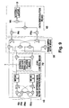
- Fig. 31 depicts a schematic configuration of a mobile unit telephone of CDMA (code division multiple access) cellular telephone system disclosed in US Patent No. 5103459. This mobile CDMD telephone system includes an
antenna 1 being connected via adiplexer 2 to ananalog receiver 3 and apower amplifier 4. Theantenna 1 receives SS (spread spectrum) signals from a cell-site to provide received signals to theanalog receiver 3 through thediplexer 2. Theanalog receiver 3 includes a down converter that converts the input received signals to baseband signals which are in turn converted to digital signals by an A/D (analog to digital) converter. Thus digitised baseband signals are fed to asearcher receiver 5 and digital data receivers (or data demodulator circuits) 6 and 7. - When the SS signals arrive at the receiver via a plurality of paths, there will arise timing differences for each signal of respective paths. The
data demodulator circuits - On the contrary, in response to a control signal from a
control processor 8, thesearcher receiver 5 scans a time domain in the vicinity of the reference timing of a received pilot signal, so as to detect respective pilot signals contained in the received multipath signals (signals received by way of a plurality of paths) from the cell-site. Then, thesearcher receiver 5 compares the strength of the received pilot signals, and outputs an strength signal to thecontrol processor 8 to indicate the strongest signals. - Then, the
control processor 8 provides control signals to thedata demodulator circuits - The function of the
data demodulator circuits data demodulator circuits PN generators data demodulator circuits function generator 520 for generating a Walsh function appropriate for the cell-site to communicate with this mobile unit. The Walshfunction generator 520 generates a code sequence corresponding to Walsh function allocated in response to the select signal from the control processor. As a part of a call set-up message, the select signal are transmitted from a cell-site to the mobile unit. PN codes PN,(t) and PNQ(t) output from thePN generators EX-OR gates function generator 520 provides its output to theEX-OR gates - The sequences PN1,(t) and PNα(t)are input to PN QPSK (quadrature phase shift keying)
correlator 526 for processing, and outputs ofcorrelator corresponding accumulators QPSK correlator 526 and the respective accumulators. The outputs of the accumulators are provided to aphase rotator 532. Thephase rotator 532 also receives the phase of a pilot signal from thecontrol processor 8. The phase of a received symbol is rotated in response to the phase of the pilot signal. The phase of the pilot signal is decided by the searcher receiver and the control processor. The output of thephase rotator 532 is in-phase axis data 23 to be fed into a combiner-decoder circuit 9. - The combiner-decoder circuit 9 consists of a diversity combiner circuit and an FEC decoder circuit.
- The diversity combiner circuit adjusts the timing of two received symbols into alignment, multiplies the two symbols by values corresponding to their respective relative signal strength, and simultaneously adds them together. This operation results in a maximal ratio combining diversity reception. Reference is to be made to PCT/US90/06417 disclosing a form of the diversity reception in the CDMA cellular system.
- As described hereinbefore, the conventional receiver has a configuration in which all the path signals are processed in common by the single analog receiver acting to down convert the received signals to base band digital signals. It is to be noted that the each received path signals has independent carrier phases respectively. For a single path signal, for example, COHERENT SPREAD SPECTRUM SYSTEMS, by J.K.Holmes, John Wi- ley & Son discloses a manner of controlling the phase of the received signal in the
analog receiver 3 with the aid of a carrier recovery circuit such as a Costas loop. However, in the case of a plurality path signals, it is difficult to simultaneously control the different phases of a plurality of received path signals. Therefore, any input signals to the data demodulators will inevitably contain a phase difference (or a residual phase difference after down converting) between a received path carrier and a local carrier used for down converting. - More specifically, where the modulation by the data and by the Walsh function for user identification are both BPSK (bi-phase shift keying) and the modulation for spreading is QPSK (quadrature phase shift keying), in the same manner as the modulation disclosed in the US Patent No. 5103459, then a complex envelope of transmission signal S(t) can be given as

where W(t) is a multiplexing signal being multiplexed of SS signals transmitting to each user and a pilot signal, and let d;(t), W;(t) and αi be modulation data, a Walsh function, and a constant corresponding to power allocation, to i-th user, respectively, and N be a number of multiplexing, then W-(t) is
(E represents the sum of i = 0 to N, and i = 0 corresponds to a pilot signal) - Next, let p be a received amplitude of a received path signal; and 0 be a phase difference (or a phase difference after down converting) between a received path signal carrier and local carrier used in down converting, then the complex envelope RX(t) of one of the received path signal to be demodulated at the output of the analog receiver can be expressed as

- Namely, the in-phase axis received signal RX1-(t) is a real part of RX(t), resulting in

and the quadrature axis received signal is an imaginary part of RX(t), resulting in
- These in-phase axis received signal and quadrature axis received signal are provided as input to the PN QPSK correlator.
- In Fig. 32 the
phase rotator 532 is used to eliminate the influence of a phase difference. Although the US Patent No. 5103459 does not disclose in detail a way of deciding a pilot signal phase as the reference phase of the phase rotator, the searcher receiver also includes a PN QPSK correlator and accumulators associated with the pilot signal, whereby that phase is supposedly determined through the execution of an arithmetic tan-1(sinθ / cose). Further, the phase rotation operation may be considered as a product operation of the phase compensation term exp (- je) = cose - jsine. Such phase rotation operation will adversely result in a complicated processing in which it is necessary to execute tan-1 arithmetic for finding 0 and to again find cose and sine from thus obtained e. - Further, owing to the scanning of a plurality of received paths, the searcher receiver entailed a problem that the reference phase is sensitive to the influence of noise since the averaging time for reducing the influence of noise is shortened in proportion to time period to be scanned, as compared with the case where the phase is determined by a single path signal. (In other words, as the noise is random, a longer averaging time will reduce the influence of noise, noise influence reducing effect will not be expected sufficiently with a shorter averaging time). Disadvantageously, a longer averaging time for ensuring a sufficient reduction of noise effect would elongate the time required to obtain the results of scanning over the entire time domains, resulting that a true phase difference may not be found due to a variation of link condition depending on the movement of the mobile during the elongated time.
- While on the contrary, Japanese Patent Application No. 149369/93 discloses a data demodulator circuit in which a pilot signal, contained in a specific received path signal demodulated by the data demodulator circuit, is subjected to a correlating process to extract phase difference information for compensating the influence of a phase difference. Fig. 33 depicts a phase difference information extracting section and a phase compensating section constituting the data demodulator circuit disclosed in the Japanese Patent Application No. 149369/93. In Fig. 33,
reference numerals - ao represents a constant related to a power allocation of the pilot signal. It is to be appreciated that time averaging operations exceeding one symbol time performed by the averaging sections ensure a sufficiently suppressed influence of the cross-correlation between PN and PNQ contained in the outputs of
multipliers - Since a received signal in the presence of a phase difference is defined as RX(t) = pS(t) exp-[je] as described earlier, the influence of the phase difference can be cleared by multiplying RX(t) by a phase compensation term exp[-je], which yields
-

Here, if the received signal is separated into an in-phase axis received signal and a quadrature axis received signal previous to the multiplication of the phase compensation term, the above expression can be written as
- Namely, taking notice of the right side of the above expression, a first term is in the form of the sum of a term obtained by multiplying the in-phase axis received signal by cose and a term obtained by multiplying the quadrature axis received signal by sine, whereas a second term is comprised of the sum of a product of the in-phase axis received signal and -sine and a product of the quadrature axis received signal and cose. On the other hand, the outputs of the averaging sections mean 20a, 20b, 20c and 20d are respectively p a ocose, - p a osine, p a osine and p a o cose. Accordingly, without the coefficient p a o signal processing equivalent to the above expression will be implemented by multiplying the outputs of the averaging sections mean 20a, 20b, 20c and 20d, and RX1 and RXx together in such a combination as depicted in Fig. 33 and then taking addition or subtraction on the products.
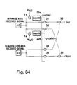
- In Fig. 33, two components on cose are respectively derived from the averaging sections mean 20a and 20d, and two components on sine are respectively derived from the averaging sections mean 20b and 20c. Fig. 34 depicts a phase compensating section of the data demodulator circuit also disclosed in the Japanese Patent Application 149369/93. Aiming at simplifying the circuitry, the phase compensating section is provided with a single multiplier and a single averaging section intended to extract in cooperation the components on cose and sine.
- In this manner, Fig. 32 configuration inconveniently necessitated such complicated processing as tan-1 arithmetic and phase rotation operation, or the reference phase was sensitive to the noise effect due to the use of a pilot phase presented by the searcher receiver scanning a plurality of received pilot signals. The circuit of Fig. 33 still remained redundant structure regardless of its intention to overcome these problems. Although the configuration depicted in Fig. 34 contrives to remove the redundancy of the Fig. 33 configuration, it has left unsolved the problem of being sensitive to the influence of the noise, due to its use of only half of the components associated with the phase difference information contained in the received signals.
- Also, the use of a plurality of data demodulator circuits for diversity reception may bring about a problem that the complexity of the receiver as a whole is increased accordingly as the configurations and processing of individual data demodulator circuits become more complicated.
- Moreover, increased influence of the noise of the phase compensation means constituting the data demodulator circuit will cause a deterioration in the demodulation characteristics of the data demodulator circuit. Thus, there arises a problem of improving the demodulation characteristics of the individual data demodulator circuits to ensure further improved demodulation characteristics in the diversity reception.
- Furthermore, in order to get the maximum performance of the maximal ratio combining diversity reception, it is necessary for the phases of the outputs of respective data demodulator circuits to adjust the phases accurately and weighted by values in response to the signal strength. However, the use of a pilot signal phase and a pilot signal level obtained by the searcher receiver would be difficult to get the maximum performance of the diversity reception due to larger influence of noise. "To adjust the phases" means herein that the phase compensation is carried out accurately.
- Also, there may be a frequency deviation generally between a transmission carrier frequency for use in a cell-site transmitter and a local oscillator output frequency used in down converting within the mobile.
- The above-described
phase difference 0 remaining after down converting can be considered to have no time variation, while if there is the frequency deviation between the received path signal carrier and the local oscillator output used in down converting, it can be expressed as

where 6 = 2πδf, and Of is a frequency deviation. Hereinafter, φ represented in the above expression will be referred to as a carrier offset. - Due to the random behavior of the noise, an elongated averaging time in the averaging sections would reduce the influence of the noise but adversely prevent the compensation of carrier offset (frequency and phase compensation) owing to the time variation for δω. A shorter time T would result in less influence of δω but also in a shortened averaging time which will in turn suppress the noise reduction effect by averaging. Thus, the conventional phase compensation means allows the problem of increased influence of noise to remain unsolved.
- Besides, as the phase compensation means of the data demodulator circuit is increasingly influenced by the noise, the demodulation characteristics of the data demodulator circuit will be degraded. Thus, there remains the problem of improving the demodulation characteristics of individual data demodulator circuit to get the further improvement of the demodulation characteristics of the diversity reception. Also there remains the problem of adjusting the phase of the outputs of the respective data demodulator circuits to get the sufficient performance of the diversity reception.
- A means of compensating the carrier offset has been, for example, reported by Takahashi, Takeishi and Onishi (IEICE, Spring National Conference A-
204, 1993) (although its modulation method differs from that of the US Patent No. 5103459). To obtain a fixed phase difference, this method comprises the steps of performing a tan-1 arithmetic for each despreading symbol to find a phase for each symbol and the differences between the successive phases, averaging the differences to find the amount of phase rotation corresponding to the frequency offset, and subtracting therefrom the amount of phase rotation corresponding to the phase found for each symbol, in order to finally average the results. - Namely, let q, (n) be a phase derived from an n-th despreading symbol, T be a symbol duration, N be an averaging number, and δφ = δωT, then δφ and 0 are obtained by an operation


where ∑ represents the sum of N = 1 to N. Then, the despreading symbols (which correspond to the outputs of theaccumulators - Also, in the case of a diversity reception using a plurality of data demodulator circuits, complicated processing required for the individual data demodulator circuit will inconveniently bring about a further increased complexity in the receiver as a whole.
- Besides, the use of the communication system disclosed in the US Patent No. 5103459 will allow a problem that the received multipath signals cause mutual interferences to degrade the receiving characteristics. More specifically, when signals transmitted from the cell-site are received through a plurality of paths, there will arise differences in the timing of the reception of the respective path signals. S(t) being orthogonal multiplexed signals based on a Walsh function, the orthogonality of the orthogonal multiplexed signals is permitted to be established only when respective receive timings coincide, whereas if the receive timings are individually different, they will become interference components to degrade the demodulation characteristics. Accordingly, there remains a problem of improving the degradation in the demodulation characteristics of the data demodulator circuit by the interference components.
- There also remains the problem of reducing the degradation in the demodulation characteristics of the individual data demodulator circuit by the interference components to further improve the demodulation characteristics of the diversity reception.
- The present invention was conceived in view of the problems involved in the prior art described above.
- It is therefore one object of the present invention to provide a data demodulator circuit for spread spectrum communication having a simpler configuration capable of eliminating a carrier offset remaining after down converting to thereby improve its demodulation characteristics.
- Another object of the present invention is to provide a data demodulator circuit for spread spectrum communication ensuring improved demodulation characteristics by removing the interference caused by pilot signals with different timing.
- Still another object of the present invention is to provide a data demodulator circuit for spread spectrum communication having a simple configuration capable of a diversity reception with the aid of a plurality of the data demodulation circuits to thereby further improve its demodulation characteristics.
- According to a first aspect of the present invention, in order to accomplish the above object, a data demodulator circuit for spread spectrum communication, demodulating data from received signal which is spread spectrum modulated with respect to the in-phase axis and the quadrature axis by a direct sequence techniques with an in-phase axis pseudo noise code and a quadrature axis pseudo noise code, respectively, said data demodulator circuit comprises a phase difference information extraction means for extracting information of phase differences, by multiplying in-phase axis received signal and quadrature axis received signal with respective pseudo noise codes used on the transmitter side, taking addition or subtraction on two of the products in a predetermined combination, and averaging the results of the addition or subtraction a phase compensation means for compensating the effect of phase differences remaining in the in-phase axis received signal and the quadrature axis received signal, by use of the phase difference information obtained by said phase difference information extraction means; and a data demodulation means for demodulating transmitted data from the outputs of said phase compensation means.
- According to a second aspect of the present invention, in order to accomplish the above object, a data demodulator circuit for spread spectrum communication, demodulating data from received signal which is spread spectrum modulated with respect to the in-phase axis and the quadrature axis by a direct sequence techniques with an in-phase axis pseudo noise code and a quadrature axis pseudo noise code, respectively, said data demodulator circuit comprises a plurality of data demodulator circuits with independent timing for spread spectrum communication according to
claim 1; a timing adjustment means adjusting the timing of the outputs of a plurality of said data demodulator circuits; an adder means for adding the outputs of said timing adjustment means; and a data decision means for deciding the transmitted data from the output of said adder means. - According to a third aspect of the present invention, in order to achieve the above object, a data demodulator circuit for spread spectrum communication, demodulating data from received signal which is spread spectrum modulated with respect to the in-phase axis and the quadrature axis by a direct sequence techniques with an in-phase axis pseudo noise code and a quadrature axis pseudo noise code, respectively, said data demodulator circuit comprises a phase difference information extraction means for extracting information of phase differences, by multiplying in-phase axis received signal and quadrature axis received signal by respective pseudo noise codes used on the transmitter side, taking addition or subtraction on two of the products in a predetermined combination, and averaging the results of the addition or subtraction; a delay means for delaying the in-phase axis received signal and the quadrature axis received signal for a suitable period of time; a frequency and phase compensation means for compensating the effect of frequency and phase offset remaining in the in-phase axis received signal and the quadrature axis received signal with time delayed by said delay means, by use of the phase difference information obtained by said phase difference information extraction means; and a data demodulation means for demodulating transmitted data from the outputs of said frequency and phase compensation means.
- According to a fourth aspect of the present invention, in order to attain the above object, a data demodulator circuit for spread spectrum communication, demodulating data from received signal which is spread spectrum modulated with respect to the in-phase axis and the quadrature axis by a direct sequence techniques with an in-phase axis pseudo noise code and a quadrature axis pseudo noise code, respectively, said data demodulator circuit comprises a plurality of data demodulator circuits with independent timing for spread spectrum communication according to
claim 3; a timing adjustment means adjusting the timing of the outputs of a plurality of said data demodulator circuits; an adder means for adding the outputs of said timing adjustment means; and a data decision means for deciding the transmitted data from the output of said adder means. - According to a fifth aspect of the present invention, provided in order to accomplish the above object, a data demodulator circuit for spread spectrum communication, demodulating data from received signal which is spread spectrum modulated with respect to the in-phase axis and the quadrature axis by a direct sequence techniques with an in-phase axis pseudo noise code and a quadrature axis pseudo noise code, respectively, said data demodulator circuit comprises a phase difference information extraction means for extracting information of phase differences, by multiplying in-phase axis received signal and quadrature axis received signal by respective pseudo noise codes used on the transmitter side, taking addition or subtract on two of the products in a predetermined combination, and averaging the results of the ddition or subtraction; a delay means for delaying the in-phase axis received signal and the quadrature axis received signal for a suitable period of time; a level control means for controlling the levels of the phase difference information obtained by said phase difference information extraction means; a frequency and phase compensation means for compensating the effect of frequency and phase offset remaining in said time delayed in-phase axis received signal and quadrature axis received signal, by use of the phase difference information whose level has been controlled by said level control means; and a data demodulation means for demodulating transmitted data from the outputs of said frequency and phase compensation means.
- According to a sixth aspect of the present invention, provided in order to accomplish the above object is a data demodulator circuit for spread spectrum communication, demodulating data from received signal which is spread spectrum modulated with respect to the in-phase axis and the quadrature axis by a direct sequence techniques with an in-phase axis pseudo noise code and a quadrature axis pseudo noise code, respectively, said data demodulator circuit comprises a plurality of data demodulator circuits with independent timing for spread spectrum communication according to
claim 5; a timing adjustment means adjusting the timing of the outputs of a plurality of said data demodulator circuits; a level adjustment means for adjusting the levels of said outputs of said plurality of data demodulator circuits with timing adjusted by said timing adjustment means; an adder means for adding the outputs of said level adjustment means; and a data decision means for deciding the transmitted data from output of said adder means. - According to a seventh aspect of the present invention, provided in order to attain the above object is a data demodulator circuit for spread spectrum communication, demodulating data from received signal which is spread spectrum modulated with respect to the in-phase axis and the quadrature axis by a direct sequence techniques with an in-phase axis pseudo noise code and a quadrature axis pseudo noise code, respectively, said data demodulator circuit comprises a phase difference information extraction means for extracting information of phase differences, by multiplying in-phase axis received signal and quadrature axis received signal by respective pseudo noise codes used on the transmitter side, taking addition or subtraction on two of the products in a predetermined combination, and averaging the results of the addition or subtraction; a delay means for delaying the in-phase axis received signal and the quadrature axis received signal for a suitable period of time; a frequency and phase compensation means for compensating the effect of frequency and phase offset remaining in said time delayed the in-phase axis received signal and the quadrature axis received signal with time delayed by said delay means, by use of the phase difference information obtained by said phase difference information extraction means; an interference amount calculation means for calculating the amounts of interference effecting on the outputs of said frequency and phase compensation means due to pilot signals with different timing; and a data demodulation means with canceler for demodulating transmitted data from the outputs of said frequency and phase compensation means, while subtracting the interference amounts calculated by said interference amount calculation means.
- According to a eighth aspect of the present invention, provided in order to attain the above object is a data demodulator circuit for spread spectrum communication, demodulating data from received signal which is spread spectrum modulated with respect to the in-phase axis and the quadrature axis by a direct sequence techniques with an in-phase axis pseudo noise code and a quadrature axis pseudo noise code, respectively, said data demodulator circuit comprises a plurality of data demodulator circuits with independent timing for spread spectrum communication according to
claim 7; a timing adjustment means adjusting the timing of the outputs of a plurality of said data demodulator circuits; an adder means for adding the outputs of said timing adjustment means; and a data decision means for deciding the transmitted data from the output of said adder means. - According to a ninth aspect of the present invention, provided in order to attain the above object is a data demodulator circuit for spread spectrum communication, demodulating data from received signal which is spread spectrum modulated with respect to the in-phase axis and the quadrature axis by a direct sequence techniques with an in-phase axis pseudo noise code and a quadrature axis pseudo noise code, respectively, said data demodulator circuit comprises a phase difference information extraction means for extracting information of phase differences, by multiplying in-phase axis received signal and quadrature axis received signal by respective pseudo noise codes used on the transmitter side, taking addition or subtraction on two of the products in a predetermined combination, and averaging the results of the addition or subtraction; a delay means for delaying the in-phase axis received signal and the quadrature axis received signal for suitable period of time; a frequency and phase compensation means for compensating the effect of frequency and phase offset remaining in the in-phase axis received signal and the quadrature axis received signal with time delayed by said delay means, by use of the phase difference information obtained by said phase difference information extraction means; a level detection means for detecting the levels of the phase difference information extracted by said phase difference information extraction means; a selective interference amount calculation means for calculating the amounts of interference effecting on the outputs of said frequency and phase compensation means due to pilot signals with different timing, controlling the results of said calculation in response to the levels detected by said level detection means, and selectively outputting the amounts of interference according to the results of said control; and a data demodulation means with canceler for demodulating transmitted data from the outputs of said frequency and phase compensation means, while subtracting the interference amounts calculated by said selective interference amount calculation means. According to a tenth aspect of the present invention, provided in order to attain the above object is a data demodulator circuit for spread spectrum communication, demodulating data from received signal which is spread spectrum modulated with respect to the in-phase axis and the quadrature axis by a direct sequence techniques with an in-phase axis pseudo noise code and a quadrature axis pseudo noise code, respectively, said data demodulator circuit comprises a plurality of data demodulator circuits with independent timing for spread spectrum communication according to claim 9; a timing adjustment means adjusting the timing of the outputs of a plurality of said data demodulator circuits; an adder means for adding the outputs of said timing adjustment means; and a data decision means for deciding the transmitted data from the output of said adder means. According to a eleventh aspect of the present invention, provided in order to attain the above object is 11. A data demodulator circuit for spread spectrum communication, demodulating data from received signal which is spread spectrum modulated with respect to the in-phase axis and the quadrature axis by a direct sequence techniques with an in-phase axis pseudo noise code and a quadrature axis pseudo noise code, respectively, said data demodulator circuit comprises a phase difference information extraction means for extracting information of phase differences, by multiplying in-phase axis received signal and quadrature axis received signal by respective pseudo noise codes used on the transmitter side, taking addition or subtraction on two of the products in a predetermined combination, and averaging the results of the addition and subtract; a delay means for delaying the in-phase axis received signal and the quadrature axis received signal for suitable period of time; a level control means for controlling the levels of the phase difference information obtained by said phase difference information extraction means; a frequency and phase compensation means for compensating the effect of frequency and phase offset remaining in the in-phase axis received signal and the quadrature axis received signal with time delayed by said delay means, by use of the phase difference information obtained by said phase difference information extraction means; an interference amount calculation means for calculating the amount of interference effecting on said level controlled outputs of said frequency and phase compensation means due to pilot signals with different timing due to signals with different timing; and a data demodulation means with canceler for demodulating transmitted data from the outputs of said frequency and phase compensation means, while subtracting the interference amounts calculated by said interference amount calculation means.
- According to a twelfth aspect of the present invention, provided in order to attain the above object is a data demodulator circuit for spread spectrum communication, demodulating data from received signal which is spread spectrum modulated with respect to the in-phase axis and the quadrature axis by a direct sequence techniques with an in-phase axis pseudo noise code and a quadrature axis pseudo noise code, respectively, said data demodulator circuit comprises a plurality of data demodulator circuits with independent timing for spread spectrum communication according to
claim 11; a timing adjustment means adjusting the timing of the outputs of a plurality of said data demodulator circuits; a level adjustment means for adjusting the levels of said outputs of said plurality of data demodulator circuits with timing adjusted by said timing adjustment means; an adder means for adding the outputs of said level adjustment means; and a data decision means for deciding the transmitted data by the output of said adder means. - According to a thirteenth aspect of the present invention, provided in order to attain the above object is a data demodulator circuit for spread spectrum communication, demodulating data from received signal which is spread spectrum modulated with respect to the in-phase axis and the quadrature axis by a direct sequence techniques with an in-phase axis pseudo noise code and a quadrature axis pseudo noise code, respectively, said data demodulator circuit comprises a phase difference information extraction means for extracting information of phase differences, by multiplying in-phase axis received signal and quadrature axis received signal by respective pseudo noise codes used on the transmitter side, taking addition or subtraction on two of the products in a predetermined combination, and averaging the results of the addition or subtraction; a delay means for delaying the in-phase axis received signal and the quadrature axis received signal for suitable period of time; a level control means for controlling the levels of the phase difference information obtained by said phase difference information extraction means; a frequency and phase compensation means for compensating the effect of frequency and phase offset remaining in the in-phase axis received signal and the quadrature axis received signal with time delayed by said delay means, by use of the phase difference information obtained by said phase difference information extraction means; a selective interference amount calculation means for calculating the amounts of interference effecting on the outputs of said frequency and phase compensation means due to pilot signals with different timing, controlling the results of said calculation in response to the levels detected through a controlled variable calculation process by said level detection means, and selectively outputting the amounts of interference in compliance with the results of said control; and a data demodulation means with canceler for demodulating transmitted data from the outputs of said selective frequency and phase compensation means, while subtracting the interference amounts calculated by said interference amount calculation means.
- According to a fourteenth aspect of the present invention, provided in order to attain the above object is a data demodulator circuit for spread spectrum communication, demodulating data from received signal which is spread spectrum modulated with respect to the in-phase axis and the quadrature axis by a direct sequence techniques with an in-phase axis pseudo noise code and a quadrature axis pseudo noise code, respectively, said data demodulator circuit comprises a plurality of data demodulator circuits with independent timing for spread spectrum communication according to
claim 13; a timing adjustment means adjusting the timing of the outputs of a plurality of said data demodulator circuits; a level adjustment means for adjusting the levels of said outputs of said plurality of data demodulator circuits with timing adjusted by said timing adjustment means; an adder means for adding the outputs of said level adjustment means; and a data decision means for deciding the transmitted data from the output of said adder means. According to a fifteenth aspect of the present invention, provided in order to attain the above object is a method for data demodulation in a demodulation apparatus for spread spectrum communication which demodulates data from received signal which is spread spectrum modulated with respect to the in-phase axis and the quadrature axis by a direct sequence technique with an in-phase axis pseudo noise code and a quadrature axis pseudo noise code, respectively, said method comprises the steps of multiplying in-phase axis received signal and quadrature axis received signal with respective pseudo noise codes used on the transmitter side; taking addition or subtraction on two of the products in predetermined combination; extracting information of phase differences by averaging the results of the addition or subtraction; and compensating the effect of phase differences remaining in the in-phase axis received signal and the quadrature axis received signal by use of the phase difference information. - According to a sixteenth aspect of the present invention, provided in order to attain the above object is the method of data demodulation of
claim 15, further comprising before the compensating step, the step of: delaying the in-phase axis received signal and the quadrature axis received signal for a suitable period of time; and wherein the compensating step compensates the effect of frequency and phase offset remaining in the in-phase axis received signal and the quadrature axis received signal with time delayed by the quadrature axis received signal with time delayed by the delaying step, by use of the phase difference information. - According to a seventeenth aspect of the present invention, provided in order to attain the above object is the method of data demodulation of claim 16, further comprising before the compensating step, the step of: controlling the levels of the phase difference information.
- According to a eighteenth aspect of the present invention, provided in order to attain the above object is the methods of data demodulation of claim 16, further comprising the steps of: calculating the amounts of interference effecting on the frequency and phase compensation due to pilot signals with different timing; and demodulating transmitted data by subtracting the interference amounts.
- According to a nineteenth aspect of the present invention, provided in order to attain the above object is the method of data demodulation of claim 18, further comprising before the calculating step, the step of: detecting the levels of the phase difference information; selecting the amounts of interference according to the levels of the phase difference information.
- According to a twelfth aspect of the present invention, provided in order to attain the above object is the method of data demodulation of claim 18, further comprising before the compensating step, the step of: controlling the levels of the phase difference information.
- According to a twenty-first aspect of the present invention, provided in order to attain the above object is the method of data demodulation of
claim 20, further comprising before the demodulating step, the step of: selecting the amounts of interference according to the levels of the phase difference information. - According to a twenty-second aspect of the present invention, provided in order to attain the above object is the method of data demodulation of
claim 15, further comprising the steps of: adjusting the timing of outputs of a plurality of the demodulation apparatus; adding the outputs of a plurality of the demodulation apparatus; and deciding the transmitted data. - These and other objects and advantages of the present invention will become more apparent, when viewed in conjunction with the following drawings, in which
- Fig. 1 is a configurational diagram of a data demodulator circuit in accordance with an embodiment of the present invention;
- Fig. 2 is a configurational diagram of an averaging section;
- Fig. 3 depicts a configuration of a data demodulator circuit in accordance with another embodiment;
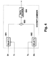
- Fig. 4 depicts a configuration of a diversity combiner circuit;
- Fig. 5 illustrates a data demodulator circuit configured in accordance with a further embodiment;
- Fig. 6 illustrates a data demodulator circuit configured in accordance with still another embodiment;
- Fig. 7 is a configurational diagram of a data demodulator circuit in accordance with a still further embodiment;
- Fig. 8 is a configurational diagram of a controlled variable calculating section;
- Fig. 9 depicts a configuration of a data demodulator circuit in accordance with yet another embodiment;
- Fig. 10 depicts a configuration of a data demodulator circuit in accordance with a yet further embodiment;
- Fig. 11 illustrates a data demodulator circuit configured in accordance with yet still another embodiment;
- Fig. 12 illustrates a data demodulator circuit configured in accordance with a yet still further embodiment;
- Fig. 13 is a configurational diagram of an interference amount calculating section;
- Fig. 14 is a configurational diagram of a data demodulator circuit in accordance with another embodiment of the present invention;
- Fig. 15 depicts a configuration of a data demodulator in accordance with still another embodiment;
- Fig. 16 depicts a configuration of a data demodulator in accordance with yet another embodiment;
- Fig. 17 illustrates a data demodulator circuit configured in accordance with yet still another embodiment;
- Fig. 18 illustrates a configuration of a level detector;
- Fig. 19 is a configurational diagram of another interference amount calculating section;
- Fig. 20 is a configurational diagram of a data demodulator circuit in accordance with a further embodiment;
- Fig. 21 depicts a configuration of a data demodulator circuit in accordance with a still further embodiment;
- Fig. 22 depicts a configuration of a data demodulator circuit in accordance with a yet further embodiment;
- Fig. 23 illustrates a data demodulator circuit configured in accordance with a yet still further embodiment;
- Fig. 24 illustrates a configuration of a further interference amount calculating section;
- Fig. 25 is a configurational diagram of a data demodulator circuit in accordance with another embodiment of the present invention;
- Fig. 26 is a configurational diagram of a data demodulator circuit in accordance with a further embodiment;
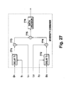
- Fig. 27 depicts a configuration of another diversity combiner circuit;
- Fig. 28 depicts a configuration of a data demodulator circuit in accordance with still another embodiment;
- Fig. 29 illustrates a configuration of still another interference amount calculating section;
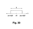
- Fig. 30 is a diagram for illustrating a symbol timing;
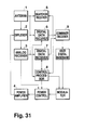
- Fig. 31 is a block diagram of a conventional transmitter-receiver;
- Fig. 32 is a configurational diagram of a data demodulator circuit employed in the conventional transmitter-receiver;
- Fig. 33 shows a configuration of a phase difference information extracting section and a phase compensating circuit constituting another conventional apparatus; and
- Fig. 34 shows a configuration of a phase difference information extracting section and a phase compensating circuit contained within a further conventional apparatus.
- Exemplary embodiments of a data demodulator circuit for spread spectrum communication in accordance with the present invention will now be described with reference to the accompanying drawings.
- Referring first to Fig. 1 of the drawings, depicted is a data demodulator circuit configured in accordance with the present invention. In Fig. 1, input to a phase difference information extraction means generally designated at 10 are an in-phase axis received signal RX1 and quadrature axis received signal RXQ along with an in-phase axis pseudo noise code PN and an quadrature axis pseudo noise code PNQ, from which is extracted information of phase difference by averaging sections meanC 20 and
meanS 25. A phase compensation means 30 makes use of the thus extracted phase difference information to compensate for the influence of the phase difference remaining on RX(t) and RXQ(t) after down converting, and outputs phase compensated in-phase axis component and quadrature axis component. In a data demodulation means generally designated at 40, the in-phase axis component and quadrature axis component are respectively multiplied by the in-phase pseudo noise code PN and quadrature pseudo noise code PNQ, and the respective products are added together through anadder 43. Then, the output of theadder 43 is multiplied by a Walsh function assigned to a mobile, and the product is accumulated for a symbol duration through anaccumulator 45. It is to be noted throughout this specification that the output of theaccumulator 45 is provided to a data decision means for deciding the data, or alternatively provided to a diversity combiner circuit and, after the diversity reception, further to the data decision means. - A more detailed action of the data demodulator circuit depicted in Fig. 1 will be described below. It is to be appreciated that since among the previously mentioned objects of the present invention the object to be achieved herein lies in conveniently compensating the
phase difference 0 remaining after the detection with a simple configuration, description is made of a case where δω is sufficiently small (φ = 0). Consideration will be given only to a path signal which the data demodulator circuit is tracking and receiving although a plurality of received path signal are contained in the in-phase axis received signal and the quadrature axis received signal. It is reported that the interference caused by the received path signals having different timing behaves like a Gaussian noise (at the accumulator output) upon demodulation (written by Allen Salmasi and Klein S. Gil- housen, entitled ON THE SYSTEM DESIGN ASPECTS OF CODE DIVISION MULTIPLE ACCESS (CDMA) APPLIED TO DIGITAL CELLULAR AND PRESONAL COMMUNICATIONS NETWORKS, 41st IEEE Vehicular Technology Conference). - As discussed earlier in the related arts, the in-phase axis received signal RX(t) and quadrature axis received signal RXQ(t) are respectively written as:


- The outputs of
multipliers adder 15 is

- Similarly, the outputs of the
multipliers 

- The outputs of the
adder 15 and 16 are provided as inputs to the averaging sections meanC 20 andmeanS 25 respectively. As compared with the conventional configurations depicted in Fig. 33 and 34, cose extracted components and sine extracted components are respectively added coherently (or in the same direction on vectror) by the adders prior to inputting to the averaging sections. On the contrary, noise input to the respective adders are added at random due to their mutual independence. Thus, the same averaging time would allow an extraction of the phase difference information to be less influenced by the noise. - Fig. 2 depicts a detailed configuration of the averaging sections meanC 20 and
meanS 25. The output of theadder 15 or 16 is input to anaccumulator 21 included within theaveraging section meanC 20 ormeanS 20, and is integrated (accumulated) over one symbol duration T. The integral for the averaging section mean C20 can be written as
(where f represents the integral over one symbol duration). If the integral time is a symbol duration T, then the integral result becomes zero without Wo (t) [ = 1 ] by virtue of the orthogonality of the Walsh function. Inasmuch as i = 0 leads to a Walsh function assigned to a pilot signal which is unmodulated (do = 1), theaveraging section meanC 20 yields the output of 2Tpao cose. In the same manner, the output of themeanS 25 results in 2Tpao sine. - The outputs of the
accumulator 21 also include other multipath signals or noise components arising from, e.g., thermal noise, so that the accumulator outputs are provided to shiftregisters adder 24 to decrease the influence of the noise. The shift register acts to shift in sequence the accumulator outputs which are to be input at intervals of T. Although a two-stage shift register is shown employed in this embodiment, the number of stages should be set optimally depending on the signal strength, phase jitter in the received signal arising from the movements of mobiles, and so on. Interposed between theaccumulator 21 and theshift register 23a is amultiplier 22 serving as a weighting circuit for normalization in which a coefficient is set to 1/(2T.m) with m being the number of inputs to the adder 24 (the number of steps in the register = m - 1). The outputs of theadder 24 less influenced by the noise are outputs pao cose, pao sine of the averaging sections meanC 20 andmeanS 25, in other words, the outputs of the phase difference information extracting means. - As in the conventional examples depicted in Figs. 33 and 34, there is an action compensating for the influence of a residual phase after down converting contained in a received signal, by use of the phase difference information extracted by the phase difference information extraction means. The
adder 35 outputs p2aoS,(t) obtained by adding to pS,(t) a coefficient pao, while theadder 36 outputs p2aoSQ(t), as discussed previously. The outputs of theadders - In the data demodulation means, the in-phase axis components are multiplied by PNI(T) whereas the quadrature axis components are multiplied by PNQ(t), and the thus obtained products are added together to derive the following output.

- Then, the
multiplier 44 acts to multiply the output of theadder 43 by the Walsh function W;(t) assigned to the mobile, resulting in
which is in turn output to theaccumulator 45. Theaccumulator 45 executes the accumulation of outputs of themultiplier 44. Due to the orthogonality of the Walsh function, αIdI(t)WI(t) is only extracted from among the multiplexed signal at the accumulator output, with the result that 2ρ2α0aIdI(t) is the output of the data demodulation means. - Although disclosed herein is a manner of executing the normalization by the
multiplier 22 between the accumulator and the shift register, the normalization may be carried out at the accumulator input or the adder output, or separately at a plurality of points. The normalization can be performed at the most appropriate point such as a point least influenced by the quantization error, depending on the number of quantization bits in the digital data or the number of stages in the shift register. - Referring next to Fig. 3, depicted is a configuration of a data demodulator in accordance with another embodiment of the present invention. First and second data demodulator circuits generally designated at 600 and 610, respectively, whose actions are substantially the same as the
embodiment 1, are allowed to act on first and second received path signal, respectively. PNµ, PNQ1 and Wi1 denote pseudo noise codes and a Walsh function, respectively, associated with the first received path signal. PN12, PNQ2 and W;2 denote pseudo noise codes and a Walsh function, respectively, associated with the second received path signal. The first and second received path signals transmitted from the same cell-site are provided with the same pseudo noise codes and Walsh function, but differ in timing from each other. Some positional relationship between the mobile and the cell-site may permit a simultaneous transmission of signals from a plurality of cell-sites to the same mobile. In such a case, however, PN,I1, PNQ1 and Wi1 will signify pseudo noise codes and a Walsh function used in a first cell-site, whereas PNI2, PNQ2 and Wi2 will signify pseudo noise codes and a Walsh function used in a second cell-site. These relationships apply to other embodiments which will be described later. - Outputs D1 and D2, respectively, of the
data demodulator circuits searcher receiver 5 or thedata demodulator circuits control processor 8, etc within the same receiver. The delay circuit outputs, after the addition by anadder 603, are provided to a data decision means 604 for data decision. In this diversity combiner circuit, the coefficients p1ai and p2ao are simultaneously multiplied when phase compensated by the phase compensation means 30 of thedata demodulator circuits - Fig. 5 is a diagram showing a configuration of a data demodulator circuit in accordance with a further embodiment of the present invention, which differs from the
embodiment 1 in the provision of delay means 50 and 51. A phase difference information extraction means 10 and a data demodulation means 40 are substantially the same as those inembodiment 1. A frequency and phase compensation means 60 is also configured in exactly the same manner as the phase compensation means 30, but differently referenced since the former enables frequency deviation to be compensated. The object of this embodiment, among the objects previously set forth, is to advantageously eliminate with a simple configuration, the influence of a carrier offset which may remain after the detection. The principle of embodiment of the Fig. 5 will be described hereinbelow. - With a carrier offset present, an in-phase axis received signal and a quadrature axis received signal are respectively given as


where φ = δωt + 0 represents a time function. As seen in Fig. 30, if an n-th symbol is present over a period of time (n - 1/2)T to (n + 1/2)T, then an average phase angle φ (n) of the n-th symbol can be written as
- The
accumulator 21 will take an operation time T with the result that there is a phase difference of only δφ between carrier offsets φ (n + 1) contained in RX1 (t) and RXQ(t) even if theaccumulator 21 directly output to frequency and phase compensation means 60 without averaging by theadder 24 in Fig. 2. Theadder 24 is intended to decrease the influence of noise, when the two-stage shift register is used which will average the phases of φ(n), φ(n-1), and φ(n -2) tends to cause a further increase in the phase difference with respect to the residual carrier offset φ (n + 1) contained in RX(t) and RXQ(t). However, if phase compensation is applied to an in-phase axis received signal and a quadrature axis received signal obtained by 2 symbol time delaying RX1(t) and RXQ(t), instead of RX,(t) and RXQ(t), based on the phase difference information extracted from the phase difference information extraction means, then the residual carrier offset of 2 symbols ago, when it is q) (n-1), will coincide with the carrier offset derived from the output of theadder 24. In consequence, if the delay time Td of the delaying means 50 and 51 is equal to 2T, then the influence of the carrier offset can be eliminated even if there may be a phase rotation δφ arising from the frequency deviation. All that is required in this embodiment against the frequency departure, is to provide the delay means, not to execute a tan-1 operation, which will lead to a simple configuration and decrease the amount of operation. It is to be noted that the delay means which is comprised of, e.g., a shift register must be shifted every at least one chip time and provided with the number of steps corresponding to the chip time duration and the delay time. - The action of the embodiment of Fig. 5 will be described hereinbelow. In the case where the shift register 23 includes two stages, by using a relationship

the output of theadder 24 located within theaveraging section meanC 20 can be expressed as
- Similarly, using a relationship

and the output of theadder 24 lying within the averaging section means 25 can be given as
- Accordingly, let the time delay Td of the delay means 50 and 51 be 2T (2 symbol time), then the carrier offset remaining after down converting, when it is φ (n-1), will coincide with the outputs derived from the
adder 24. Hence, in the same manner as theembodiment 1, the influence of the carrier offset can be removed through the frequency and phase compensation means, exclusive of the coefficient pao (1 /3) [1 + 2 cos (δφ)]. - A component (1 /3)[1 + 2 cos (δφ)] of the coefficient can be considered as a loss depending on δφ and caused by an averaging operation. With δφ = 0 (q) = 0) the coefficient will result in pao (no loss), and a carrier offset including only a
phase difference 0 will lead to just the same effects as in the case of theembodiment 1. With the increase of δφ the value of the coefficient will be decreased, and finally becomes zero at δφ = + 2π/3, when no phase difference information is extracted. Therefore, in the case of a two-stage shift register, the compensation limit is defined as δφ (the amount of phase rotation per symbol) = 2π/3 rad. - The compensation limit varies depending on the number of steps of the shift register. In the case where the number of steps in the shift register is, for example, four (that is, the number of times of addition in the adder is five), the outputs of the averaging sections meanC 20 and
meanS 25 will be respectively given as

- This will lead to the necessity of setting the delay time Td of the delay means 50 and 51 to 4T. In this instance, an increase in the number of averaging steps will allow the influence of the noise to be further reduced. It is to be appreciated that δ φ at the compensation limit is 0.4π rad so that the maximum frequency offset amount to be compensated for will decrease. On the contrary, in the case where the number of stages in the shift register is one, the outputs of the
averaging section meanC 20 andmeanS 25 can be respectively given as

- This will lead to the necessity of setting the delay time Td of the delay means 50 and 51 to 1.5T. In this instance, a decrease in the number of averaging steps will allow the influence of the noise to be increased, but δ φ at the compensation limit is π so that the maximum frequency offset amount to be compensated for will increase. The output of the phase difference information extraction means 10 can be derived from the formula for summation of trigonometric functions, in the same manner as in the case of the two-stage shift register.
- Although the above description has been made with the compensation limit being δ φ where the output of the phase difference information extraction means 10 can be zero, it will be apparent that the phase difference information extraction means 10 is gradually decreasing output values accordingly as the compensation limit is approached. Also when the carrier offset becomes greater, the outputs (correlative values) of the
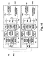
accumulators 21 within the averaging sections meanC 20 andmeanS 25 decrease. The amounts of decreasing in the outputs are reported in, for example, Transaction of IEICE, Vol. J69 - B No. 11, pp. 1540 - 1547. On the contrary, the influence of the noise will be gradually increased due to loss incidental to the averaging operation and to reduction in the accumulator outputs, since noise components contained in the outputs of theaccumulators 21 are independent of the carrier offset. For the mobile, care must be taken of the above when deciding the number of stages in the shift register. To this end, it is preferable that the decision be so made as to fit the actual system, taking into consideration the degree of loss, the lowered accumulator outputs (correlative values), noise influence reduction effects attendant on the increase of the number of stages in the shift register, compensation limit of the carrier offset, and so on. When delay means such as 50 and 51 are introduced, it should be noted that pseudo noise codes used in data demodulation means such as 40 must be time delayed corresponding to delay time Td throughout this specification. - Fig. 6 depicts a configuration of a data demodulator circuit in accordance with still another embodiment of the present invention. Shown are first and second data demodulator circuits generally designated at 620 and 630, respectively, whose actions are substantially the same as those of
embodiment 3. By virtue of delay means 50 and 51 provided in each of thedata demodulator circuits embodiment 2, the same effects irrespective of the presence of any frequency deviation, thereby eliminating the influence of the carrier offset with a simple configuration and implementing a preferred maximal ratio combining diversity action. - Fig. 7 illustrates a configuration of a data demodulator circuit in accordance with a still further embodiment of the present invention, which differs from
embodiment 3 in the interposition of a level control means 70 between a phase difference information extraction means 10 and a frequency and phase compensation means 60, although otherwise coincident withembodiment 3. In the description ofembodiment 3, the outputs of the averaging sections meanC 20 andmeanS 25, if the number of stages in the shift register is two, have been respectively given as -


embodiment 5 is so configured as to ensure substantially the same effects asembodiment 3 with respect to the compensation for the carrier offset and to prevent any amplitude conversion at the time of compensation. - The level control means 70 was provided to cope with a lower number of bits than described above, which includes a control
variable calculating section 80 for calculating a control variable from the output of the phase difference information extraction means and includesmultipliers variable calculating section 80 is shown in Fig. 8. The outputs of the phase difference information extraction means are respectively fed to squaring means 81 and 82 which find a sum-square with the aid of anadder 83. By finding the sum-square, a square value of the coefficients is provided as the adder output, due to the identity of the coefficients associated with cosine and sine terms which carry phase difference information in the outputs of the averaging sections meanC 20 andmeanS 25. Then a square root calculating means 84 calculates a square root of the square value of the coefficients to thereby obtain a magnitude of the coefficients. The square root calculation means may be used as a level monitor. Afterwards, aninverse circuit 85 finds the inverse of the magnitude of the coefficients to calculate a control variable. Thus, the output of the control variable calculating section which is the inverse of the magnitude of the coefficients is multiplied through themultipliers - Fig. 9 depicts a configuration of a data demodulator circuit in accordance with yet another embodiment of the present invention, which differs from
embodiment 5 in the point that the delay means 50 and 51 are absent. Such an arrangement can be taken in the case where the carrier offset is regarded as a phase offset 0 with a sufficiently minute δφ. - A sufficiently minute oq, would be the case, for example, where the accuracy of the local oscillator is good enough or where δφ is corrected by other means. In this instance, there is no need to provide any delay means, which will lead to a reduction in the dimensions of the circuit.
Embodiment 7 Fig. 10 depicts a configuration of a data demodulator circuit in accordance with a further embodiment of the present invention, in which generally designated at 640 and 650 are respectively first and second data demodulator circuits whose actions are substantially the same as in theembodiment 5. The data demodulatorcircuits data demodulator circuits multipliers adder 775 and intended to execute the multiplication of the coefficient proportional to the amplitude. The coefficient proportional to the amplitude is derived from the square root calculation means 84 of the controlled variable calculating section depicted in Fig. 8, so that the maximal ratio combining diversity action can be easily implemented without any additional means and processes. It will be understood that the positional relationship may be reversed between the delay means 771 and themultiplier 773. The same can be said of that between the delay means 772 and themultiplier 774. - Fig. 11 depicts yet another embodiment of a data demodulator circuit configured in accordance with the present invention, differing from
embodiment 7 in the point that it excludes the delay means 50 and 51. Such an arrangement can be taken insofar as the carrier offset is regarded as a phase offset 0 with a sufficiently minute δφ. A sufficiently minute δφ would be the case, for example, where the accuracy of the local oscillator is good enough or where oq, is corrected by other means. This will require no delay means and accomplish the reduction in size of the circuit. - Fig. 12 depicts a still further embodiment of a data demodulator circuit configured in accordance with the present invention.
- Although in the
embodiments 1 to 8 notice has been exclusively taken of received path signal, actually there also exist path signals with different timing, or signals transmitted from other cell-sites. These can be regarded as random noises causing a deterioration of the data demodulation characteristics. It is however difficult to calculate a noise quantity at the time of demodulation due to the necessity of processing enormous operations. Nevertheless, the mobile continues to constantly monitor pilot signals contained in the received path signals so as to obtain information on reception timing, phases, etc., of at least pilot signals having higher levels. Among the objects set forth previously, the object of this embodiment is to provide a demodulator circuit allowing, based on the information on reception timing, phases, etc., of the pilot signals, a calculation of the amount of interference caused by pilot signals with different timing, and including a demodulation means capable of eliminating the interference amount. Besides from Fig. 5 indicative ofembodiment 3, Fig. 12 shows an interference amount calculation means as well as a data demodulation means with canceler having acanceler 91 for eliminating the interference amount. Substantially the same asembodiment 3 are the other constituent elements such as a phase difference information extraction means 10, frequency and phase compensation means 60, and delay means 50 and 51. - Description will be first made of the interference due to the pilot signals having different timing.
- Now consider a case where a receiver receives two path signals with different timing. An earlier timing signal and a later timing signal are referred to as an forward wave and a delay wave, respectively.
- A complex envelope RX(t) of a signal provided as the input to the data demodulator circuit can be expressed as

where pi and φ1 denote a received amplitude and a carrier offset, respectively, of the forward wave; p2 and φ2 denote a received amplitude and a carrier offset, respectively, of the delay wave; and denotes a difference in timing between the forward wave and the delay wave. In the event that the demodulator circuit of Fig. 12 is acting on the forward wave, the frequency and phase compensation means 10, as previously explained inembodiment 3, will execute an operation RX(t) * pi ao exp(- jφ1,) with respect to RX(t), with result that the output of the frequency and phase compensation means 10 is provided as
where a first term of the above expression represents a desired component, and a second term represents an interference factor arising from path signal with different timing. Description will be given of a behavior of the second term which is an interference factor, because the desired component having been explained inembodiment 1. - The second term can be arranged as

In the above expression, the real component signifies an input of amultiplier 41, and the imaginary component signifies an input of amultiplier 42, with △ φ = φ 2 - φ1. In the data demodulation means with canceler, themultiplier 41 serves to multiply the multiplier input by PNI(t) with respect to the interference factor, to thereby provide an output

- Similarly, the
multiplier 42 will provide an output
- Hereinafter, such representations will be available as Wi(t) = Wi1, Wi(t + τ) = Wi2, PNI1 = PN-(t), PNQ1 = PNQ(t),PNI2 = PNI(t +τ), and PNQ2 = PNQ(t + T). The pilot signal being unmodulated, the pilot signal Wo2 contained herein W(t + τ) is all 1, and a power distribution coefficient is a o. Hence, among the interference factors contained in the outputs of the
multipliers -


adder 43, the amount of interference IDF1 caused by the delay wave pilot signal will be expressed in terms of the sum of the two expressions:
- Similarly derived is the amount of interference IDF2 caused by the delay wave pilot signal among the interference factors contained in the output of the
adder 43 within the data demodulator circuit acting on the delay wave.
- Consequently, upon condition that the mobile is capable of calculating IpF (= IDF1 = IDF2) therewithin, then the interference associated with the delay wave pilot signal can be eliminated by subtracting IpF from the output of the
adder 43 of the data demodulator circuit acting on the advance wave, whereas the interference associated with the advance wave pilot signal can be eliminated by subtracting IpF from the output of theadder 43 of the data demodulator circuit acting on the delay wave, thus accomplishing the improvement in demodulating characteristics. - Incidentally, p1ao cosφ1 and p1ao sinφ1 are derived from the averaging sections meanC 20 and
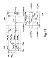
meanS 25, respectively, constituting the phase difference information extraction means 10 within the data demodulator circuit operating on the forward wave, while p2ao cosφ2 and p2ao sinφ2 are derived from the averaging sections meanC 20 andmeanS 25, respectively, constituting the phase difference information extraction means 10 within the data demodulator circuit operating on the delay wave. It is to be noted that the description herein has been made of a case, as previously explained inembodiment 3, where the averaging step attendant loss depending on the carrier offset is sufficiently small. Without direct representations in the diagrams, PNI1 and PNQ1 are delivered from a timing regenerating system of the data demodulator circuit acting on the forward wave, whereas PN12 and PNQZ are delivered from the timing regenerating system of the data demodulator circuit acting on the delay wave, where all of them should be reflected the delay time Td. - It is thus possible from the above to find IpF by the interference amount calculation means depicted in Fig. 13. Although Fig. 13 illustrates a mathematical operation for deriving IpF from the respective components described above, the same effects may be presented by a software calculation.
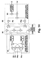
- Fig. 14 depicts another embodiment of a data demodulator circuit configured in accordance with the present invention, differing from embodiment 9 in the point that it lacks the delay means 50 and 51. This is an arrangement taken when the carrier offset can be regarded as a phase offset 0 with a sufficiently minute δφ. The sufficiently minute δφ would occur in the case, for example, where the local oscillator has a good enough accuracy or δφ is corrected by other measures, leading to a reduction in size of the circuit.
- Fig. 15 depicts a configuration of still another embodiment of a data demodulator circuit in accordance with the present invention. Generally designated at 680 and 690 are respectively first and second data demodulator circuits acting on, respectively, forward wave and delay wave. The actions of the
data demodulator circuits circuit 680, whereas p2ao cosφ2 and p2ao sinφ2 are given by a phase difference information extraction means of thecircuit 690. In the same manner, PNI1 and PNQ1 are delivered from a timing regenerating system of thecircuit 680 while PN12 and PNQ2 are delivered from a timing regenerating system of thecircuit 690. Output D1 and D2, respectively, of thedata demodulator circuits embodiment 4, in response to powers of the pilot signals contained in the received path signals having different timing. - Fig. 16 depicts yet another embodiment of a data demodulator circuit configured in accordance with the present invention, differing from
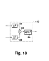
embodiment 11 in the exclusion of delay means 50 and 51. This is an arrangement available when the carrier offset can be regarded as a phase offset 0 with a sufficiently minute δφ. The sufficiently minute δφ would occur in the case, for example, where the local oscillator has a good enough accuracy or δφ is corrected by other measures, leading to a reduction in size of the circuit. - Fig. 17 is a diagram showing yet another embodiment of a data demodulator circuit in accordance with the present invention, which differs from Fig. 12 depicting embodiment 9 in the point that it includes a level detection means 140 between a phase difference extraction means 10 and a frequency and phase compensation means 60. An interference amount calculation means in this embodiment has a configuration depicted in Fig. 19, being different from Fig. 13 illustrating embodiment 9 in the point that it further includes a
control section 160 and aselector 200. Although the elimination of interference can be accomplished when the influence of noise has been satisfactorily reduced at the output of the phase difference extraction means 10, a lower signal level, for example, would increase the influence of the noise and the output of the phase difference information extraction means 10 may be more greatly affected by the noise. Since, in such an instance, an interference amount obtained by the interference amount calculation means is also being greater influenced by the noise, a subtraction of IDF in an adder 92 of Fig. 17 might possibly cause a deterioration in the receiving characteristics. - In order to prevent such deterioration in the receiving characteristics, input to the
control section 160 of Fig. 19 is a level detected by thelevel detecting means 140. Then, if either one of detection levels piao and p2ao of the data demodulator circuits acting on the forward wave and the delay wave, respectively, drops below a threshold level (Lo) simultaneously input to the control section, control signals are issued from the control section to multipliers and adder/subtracters ofsections selector 200 receives a select signal, thereby permitting the interference amount calculation means to output IpF = 0. If IpF = 0 is provided as input to theadder 91, then the canceling action will be effectively ceased to allow a prevention of deterioration in characteristics. Referring to Fig. 18, shown is a detailed configuration of alevel detector 150 devoted to level detection and including only a sum-squaring means and a square root calculation means. - Fig. 20 depicts a further embodiment of a data demodulator circuit in accordance with the present invention, differing from the
embodiment 13 in the point that the delay means 50 and 51 are excluded therefrom. This arrangement is available when the carrier offset can be regarded as a phase offset 0 with a sufficiently minute δφ. The sufficiently minute δφ would occur, for example, when the local oscillator has a good enough accuracy or when δφ is corrected by other measures, leading to a reduction in size of the circuit. - Fig. 21 depicts a still further embodiment of a data demodulator circuit configured with the present invention. Generally designated at 720 and 730 are data demodulator circuits which operate on forward wave and delay wave, respectively, and whose actions are substantially the same as the
embodiment 13. More specifically, piao cosφ1 and piao sinφ1 of Fig. 19 are supplied from a phase difference information extraction means constituting thecircuit 720, while p2ao cosφ2 and p2ao sinφ2 are supplied from a phase difference information extraction means constituting thecircuit 730. Similarly, PNI1 and PNQ1 are delivered from a timing regenerating system associated with thecircuit 720, while PN12 and PNQ2 are delivered from a timing regenerating system associated with thecircuit 730. piao and p2ao are respectively fed from level detecting means of thecircuits data demodulator circuits - Fig. 22 depicts a yet further embodiment of a data demodulator circuit configured in accordance with the present invention, which differs from the
embodiment 15 in the point that it includes no delay means 50 and 51. This arrangement is available when the carrier offset can be regarded as a phase offset 0 with a sufficiently minute δφ. The sufficiently minute δφ would occur in the case, for example, where the local oscillator has a good enough accuracy or δφ is corrected by other measures, leading to a reduction in size of the circuit. - Fig. 23 is a diagram depicting a configuration of a still further embodiment of a data demodulator circuit in accordance with the present invention. In addition to the configuration depicted in Fig. 7 indicative of the
embodiment 5, this embodiment is arranged to include an interference amount calculation means illustrated in Fig. 24 by which the amounts IDF1 or IDF2 of interference are eliminated through anadder 91 constituting a data demodulation means 90 with canceler. IDF1 is input when the circuit shown in Fig. 23 acts on forward wave, whereas IDF2 is input when it acts on delay wave. Namely, when the data demodulator circuit includes a level control means, the Interference amount IDF1 and IDF2 may result in different values from those in Fig. 12 depicting the embodiment 9 not including level control means. Nevertheless, as long as it is noted that the outputs of the level control means with respect to RX (t) are not p 1 a o exp (- jφ 1) and p 2 a o exp (-jφ2), respectively, m but exp (-jφ1) and exp (- jφ2), respectively, IDF1 and IDF2 will simply obtained from the method illustrated in the embodiment 9 -


- It is thus possible to find IDF1 and IDF2 by the interference amount calculation means depicted in Fig. 24. Although Fig. 24 illustrates a mathematical operation for deriving IDF1 and IDF2 from the respective components described above, the same effects may be presented by a software calculation.
- Fig. 25 depicts another embodiment of a data demodulator circuit in accordance with the present invention, differing from embodiment 17 in the point that it does not include the delay means 50 and 51. This is an arrangement available when the carrier offset can be regarded as a phase offset 0 with a sufficiently minute δφ. The sufficiently minute δφ would occur in the case, for example, where the local oscillator has a good enough accuracy or δφ is corrected by other measures, leading to a reduction in size of the circuit.
- Fig. 26 depicts a configuration of a further embodiment of a data demodulator circuit in accordance with the present invention. This embodiment includes
data demodulator circuits circuit 760 issues cos φ1 and sin φ1 of Fig. 24, while a level control means of thecircuit 770 issues cos φ2 and sin φ2. In the same manner, a timing regenerating system associated with thedemodulator circuit 760 issues PNI1 and PNQ1, while a timing regenerating system associated with thecircuit 770 issues PN12 and PNQ2. Also, piao and p2ao are respectively obtained by controlled variable calculating sections within the level control means constituting thecircuits - Thus, the configuration of Fig. 23 or Fig. 26 will ensure for the use of a level controlled frequency and phase compensation means that demodulating characteristics are improved by finding the amount of interference caused by pilot signals with different timing and canceling it within the data demodulator means with a canceler. Consequently, with a lower number of quantized bits, effective action will be ensured on the carrier offset and on the interference arising from the pilot signals with different timing, resulting in the implementation of a preferred maximal ratio combining diversity reception.
- Fig. 28 depicts still another embodiment of a data demodulator circuit in accordance with the present invention, differing from the embodiment 19 in the point that the delay means 50 and 51 are excluded therefrom. This arrangement is permitted to be employed when the carrier offset can be regarded as a phase offset 0 with a sufficiently minute δφ. The sufficiently minute δφ would occur when, for example, the local oscillator has a good enough accuracy or δφ is corrected by other measures, contributing to a reduction in size of the circuit.
- Fig. 23 depicts a configuration of a still further embodiment of a data demodulator circuit in accordance with the present invention. The relationship between the
embodiments 17 and 21 will be similar to that established between theembodiments 9 and 13. Namely, theembodiment 21 aims to provide a data demodulator circuit allowing a prevention of degradation in characteristics, by effectively ceasing a canceling action in the case where the canceling action may adversely degrade the reception characteristics, in response to a level obtained by the level control means of the embodiment 19. Thus, an interference amount calculation means depicted in Fig. 29 is used. The interference amount calculation means of Fig. 29 is comprised of the interference amount calculation means of Fig. 24 with anadditional control section 160 andselector 230. Thecontrol section 160 issues control signals to multiplier-adder-subtracter sections control section 160 issues a select signal to theselector 230, allowing IOF1, IOF2 = 0 to be output for the effective stop of the canceling action, to thereby prevent a degradation in characteristics. - A threshold level Lo is appropriately determined from a received S/N ratio, the magnitude of ao, etc., in consideration of a value that may not be expected the removal of interference.
- Figs. 25 and 29 depict yet another embodiment of a data demodulator circuit configured in accordance with the present invention and differing from the
embodiment 21 in the point that delay means 50 and 51 are not included. This is an arrangement available when the carrier offset can be regarded as a phase offset 0 with a sufficiently minute δφ. The sufficiently minute δφ would occur in the case, for example, where the local oscillator has a good enough accuracy or δφ is corrected by other means, leading to a reduction in size of the circuit. Embodiment 23 - Fig. 26 is a configurative diagram depicting a yet further embodiment of a data demodulator circuit in accordance with the present invention. The configuration of interference amount calculation means used in first and second
data demodulator circuits embodiment 21. Thus, the outputs of the data demodulator circuits are provided to the diversity combiner circuit depicted in Fig. 27 so as to eliminate the influence of the carrier offset irrespective of a lower number of bits and to cancel the influence of the interference arising from pilot signals with different timing and further to prevent the canceling action from causing a degradation in characteristics when the received path signal is a low level. - Fig. 28 also depicts a yet further embodiment of a data demodulator circuit configured with the present invention, which differs from the embodiment 23 in the point that it does not include the delay means 50 and 51. This arrangement is available if the carrier offset can be regarded as a phase offset 0 with a sufficiently minute bq). The sufficiently minute oq, would occur when, for example, the local oscillator has a good enough accuracy or δφ is corrected by other means, leading to a reduction in size of the circuit.
- Although in the above-described embodiments describes for only two received paths, associated with forward wave and delay wave, the same configuration is applicable when there are three or more paths having a greater strength by calculating the amount of interference to remove the influence of interference caused by pilot signals with different timing. More specifically, it is possible for the data demodulator circuit acting on a first path signal to eliminate the interference, by calculating the amount of interference arising from a pilot signal contained in a second path signal and the amount of interference arising from a pilot signal contained in a third path signal individually with the respective interference amount calculation means, in the same manner as the methods disclosed in the above embodiments, and then providing the results as input to the
adder 91 of the demodulator circuit acting on the first path signal. - The same can be said of the data demodulator circuits acting on second and third path signals, respectively.
- In the case of that the total number of the data demodulator circuits is limited, it is possible for data demodulator circuits to remove the interference due to the pilot signals contained in the received path signal without allocating demodulator circuits, by calculating the amount of interference, and providing the result, as input to the adder 19, by use of the interference amount calculation means corresponding to the respective embodiments. Because it is possible to obtain components necessary for the calculation of the interference amount, by setting up such as a pseudo noise code timing regenerating means (the
embodiments 5 to 12), a phase difference information extraction means 10 (embodiments 5 to 12), a level detecting means 140 (embodiments 7 and 8), and a level control means 70 (embodiments 9 to 12). - Although disclosed in this specification is a data demodulator circuit for spread spectrum modulated signals with respect to two axes consisting of the in-phase axis and the quadrature axis (QPSK spread spectrum signals), the omission of a processing system associated with the quadrature axis spread symbols would allow the data demodulator circuit to present substantially the same effects for spread spectrum modulated signals only with respect to the in-phase axis. The action in this case will be easy to understand, assuming that PNQ, PNQ1 and PNQ2 equal to be zero over the contents disclosed in the specification.
- According to a data demodulator circuit for spread spectrum communication of the present invention, as detailed in the above embodiments, an in-phase axis received signal and a quadrature axis received signal are respectively multiplied by an in-phase axis pseudo noise code and a quadrature axis pseudo noise code, the products being subjected to an addition or subtraction and then averaged, whereby a simple configuration will ensure an extraction of phase difference information having increased immunity to noise.
- Also, as a frequency and phase compensation is operated on received signals delayed by a suitable period of time so as to allow the amount of phase rotation arising from a relative frequency deviation to be identical, thereby eliminating the influence arising from the frequency deviation by only use of the delay means without requiring any execution of such complicated processing as tan-1 arithmetic and phase rotation operations.
- Further, the level control means allows the frequency and phase compensation to be carried out at a constant level, which will ensure an effective action in the case of a restricted number of quantized bits.
- Furthermore, the interference amount calculation means and the data demodulation means with canceler serve in cooperation to remove the amount of interference caused by the pilot signals with different timing to improve the demodulating characteristics.
- Also, the action of the interference amount calculation means is allowed to be controlled in response to the amount of the detection level, thereby preventing the degradation in characteristics which may be attendant on the removal of interference when the level is small.
- Moreover, the maximal ratio combining diversity reception is performed by a diversity combiner circuit through a plurality of data demodulator circuits so as to ensure by a simple configuration a maximum ratio diversity receive action superior in characteristics including the above effects.
Claims (22)
Applications Claiming Priority (3)
| Application Number | Priority Date | Filing Date | Title |
|---|---|---|---|
| JP3870294 | 1994-03-09 | ||
| JP3870294A JP2938337B2 (en) | 1994-03-09 | 1994-03-09 | Data demodulation circuit for spread spectrum communication |
| JP38702/94 | 1994-03-09 |
Publications (3)
| Publication Number | Publication Date |
|---|---|
| EP0671820A2 true EP0671820A2 (en) | 1995-09-13 |
| EP0671820A3 EP0671820A3 (en) | 1999-06-09 |
| EP0671820B1 EP0671820B1 (en) | 2002-09-25 |
Family
ID=12532652
Family Applications (1)
| Application Number | Title | Priority Date | Filing Date |
|---|---|---|---|
| EP19950102529 Expired - Lifetime EP0671820B1 (en) | 1994-03-09 | 1995-02-22 | Spread spectrum data demodulation with phase correction |
Country Status (9)
| Country | Link |
|---|---|
| US (1) | US5787112A (en) |
| EP (1) | EP0671820B1 (en) |
| JP (1) | JP2938337B2 (en) |
| KR (1) | KR0169021B1 (en) |
| CN (1) | CN1071965C (en) |
| CA (1) | CA2141654C (en) |
| DE (1) | DE69528301T2 (en) |
| FI (1) | FI951102A (en) |
| NO (1) | NO950745L (en) |
Cited By (2)
| Publication number | Priority date | Publication date | Assignee | Title |
|---|---|---|---|---|
| GB2347324A (en) * | 1999-02-25 | 2000-08-30 | Fujitsu Ltd | Code-division multiplex using phase modulation |
| WO2001005052A1 (en) * | 1999-07-09 | 2001-01-18 | Nokia Mobile Phones | Interference suppression in a cdma receiver |
Families Citing this family (27)
| Publication number | Priority date | Publication date | Assignee | Title |
|---|---|---|---|---|
| EP0776105B1 (en) * | 1995-06-13 | 2004-08-25 | NTT DoCoMo, Inc. | Cdma demodulator |
| US5978413A (en) * | 1995-08-28 | 1999-11-02 | Bender; Paul E. | Method and system for processing a plurality of multiple access transmissions |
| JP3200547B2 (en) * | 1995-09-11 | 2001-08-20 | 株式会社日立製作所 | CDMA mobile communication system |
| JP3452735B2 (en) * | 1996-08-09 | 2003-09-29 | 株式会社鷹山 | Path diversity receiving method and apparatus for spread spectrum communication |
| JPH1070497A (en) * | 1996-08-27 | 1998-03-10 | Saitama Nippon Denki Kk | Method for synthesizing reception signal from diversity system radio equipment |
| US6335954B1 (en) * | 1996-12-27 | 2002-01-01 | Ericsson Inc. | Method and apparatus for joint synchronization of multiple receive channels |
| US5982809A (en) * | 1997-01-23 | 1999-11-09 | Cwill Telecommunications, Inc. | Method and apparatus for carrier recovery and compensation in spread spectrum communications |
| US6125136A (en) * | 1997-12-31 | 2000-09-26 | Sony Corporation | Method and apparatus for demodulating trellis coded direct sequence spread spectrum communication signals |
| US6389085B1 (en) * | 1998-01-14 | 2002-05-14 | Wavecom Electronics Inc. | Receiver combiner for spatial diversity digital communications |
| US6498784B1 (en) | 1998-10-20 | 2002-12-24 | Interdigital Technology Corporation | Cancellation of pilot and traffic signals |
| CA2282800C (en) * | 1998-11-09 | 2007-07-31 | Lucent Technologies Inc. | A coherent combining/noncoherent detection (ccnd) method and apparatus for detecting a pilot signal in a wireless communication system |
| US6470005B1 (en) * | 1998-12-29 | 2002-10-22 | Thomson Licensing Sa | Transceiver prerotation based on carrier offset |
| IL128262A0 (en) * | 1999-01-28 | 1999-11-30 | Israel State | Dsss receiver |
| US6480528B1 (en) * | 1999-06-11 | 2002-11-12 | Qualcomm Incorporated | Automatic gain control for improved decoding of multi-carrier signal |
| DE60011566T2 (en) * | 2000-04-07 | 2005-08-18 | Alcatel | Receiver for a CDMA mobile communication system |
| US7346135B1 (en) | 2002-02-13 | 2008-03-18 | Marvell International, Ltd. | Compensation for residual frequency offset, phase noise and sampling phase offset in wireless networks |
| US7263153B2 (en) | 2002-10-09 | 2007-08-28 | Marvell International, Ltd. | Clock offset compensator |
| US7246192B1 (en) | 2003-01-10 | 2007-07-17 | Marvell International Ltd. | Serial/parallel ATA controller and converter |
| KR100575938B1 (en) * | 2003-03-13 | 2006-05-02 | 한국과학기술원 | Apparatus and method for compensating frequence offset in mobile communication system |
| US8930583B1 (en) | 2003-09-18 | 2015-01-06 | Marvell Israel (M.I.S.L) Ltd. | Method and apparatus for controlling data transfer in a serial-ATA system |
| US20060200510A1 (en) * | 2005-01-31 | 2006-09-07 | Wang Cindy C | Precision cordic processor |
| CN1333533C (en) * | 2005-05-16 | 2007-08-22 | 北京北方烽火科技有限公司 | Method of frequency compensation for Direct Sequence Spread Spectrum (DSSS) mobile communication system |
| US20070111111A1 (en) * | 2005-11-15 | 2007-05-17 | Yokogawa Electric Corporation | Light measurement apparatus and light measurement method |
| CN101779509A (en) * | 2007-08-14 | 2010-07-14 | 松下电器产业株式会社 | Radio communication system, scheduling method, radio base station device, and radio terminal |
| WO2009137957A1 (en) | 2008-05-16 | 2009-11-19 | Yang Shitong | Exact spot welder for resistance welding |
| CN101610108B (en) * | 2009-07-15 | 2012-07-04 | 电信科学技术第一研究所 | Method for improving carrier phase jitter and waveform distortion of digital spread spectrum receiver |
| CN115567169A (en) * | 2022-12-06 | 2023-01-03 | 成都航天通信设备有限责任公司 | Demodulation and decoding method, system, equipment and storage medium under low coding rate |
Citations (2)
| Publication number | Priority date | Publication date | Assignee | Title |
|---|---|---|---|---|
| US5224122A (en) * | 1992-06-29 | 1993-06-29 | Motorola, Inc. | Method and apparatus for canceling spread-spectrum noise |
| EP0577044A1 (en) * | 1992-06-29 | 1994-01-05 | Mitsubishi Denki Kabushiki Kaisha | Phase difference correcting demodulator for a receiver for spread spectrum communication |
Family Cites Families (6)
| Publication number | Priority date | Publication date | Assignee | Title |
|---|---|---|---|---|
| US4901307A (en) * | 1986-10-17 | 1990-02-13 | Qualcomm, Inc. | Spread spectrum multiple access communication system using satellite or terrestrial repeaters |
| JPH03145833A (en) * | 1989-10-31 | 1991-06-21 | Mitsubishi Electric Corp | Demodulator for spread spectrum signal |
| GB2240240A (en) * | 1990-01-19 | 1991-07-24 | Philips Electronic Associated | Radio receiver for direct sequence spread spectrum signals |
| US5103459B1 (en) * | 1990-06-25 | 1999-07-06 | Qualcomm Inc | System and method for generating signal waveforms in a cdma cellular telephone system |
| DE4127501A1 (en) * | 1990-09-07 | 1992-03-12 | Telefunken Systemtechnik | METHOD FOR DETECTING THE FREQUENCY STORAGE IN DIGITAL MESSAGE TRANSMISSIONS |
| US5276705A (en) * | 1993-01-06 | 1994-01-04 | The Boeing Company | CCD demodulator/correlator |
-
1994
- 1994-03-09 JP JP3870294A patent/JP2938337B2/en not_active Expired - Fee Related
-
1995
- 1995-02-01 CA CA002141654A patent/CA2141654C/en not_active Expired - Fee Related
- 1995-02-08 US US08/385,284 patent/US5787112A/en not_active Expired - Fee Related
- 1995-02-22 DE DE1995628301 patent/DE69528301T2/en not_active Expired - Fee Related
- 1995-02-22 EP EP19950102529 patent/EP0671820B1/en not_active Expired - Lifetime
- 1995-02-27 NO NO950745A patent/NO950745L/en unknown
- 1995-03-02 CN CN95102472A patent/CN1071965C/en not_active Expired - Fee Related
- 1995-03-08 KR KR1019950004672A patent/KR0169021B1/en not_active IP Right Cessation
- 1995-03-09 FI FI951102A patent/FI951102A/en unknown
Patent Citations (2)
| Publication number | Priority date | Publication date | Assignee | Title |
|---|---|---|---|---|
| US5224122A (en) * | 1992-06-29 | 1993-06-29 | Motorola, Inc. | Method and apparatus for canceling spread-spectrum noise |
| EP0577044A1 (en) * | 1992-06-29 | 1994-01-05 | Mitsubishi Denki Kabushiki Kaisha | Phase difference correcting demodulator for a receiver for spread spectrum communication |
Non-Patent Citations (1)
| Title |
|---|
| PATENT ABSTRACTS OF JAPAN vol. 015, no. 367 (E-1112), 17 September 1991 & JP 03 145833 A (MITSUBISHI ELECTRIC CORP), 21 June 1991 * |
Cited By (5)
| Publication number | Priority date | Publication date | Assignee | Title |
|---|---|---|---|---|
| GB2347324A (en) * | 1999-02-25 | 2000-08-30 | Fujitsu Ltd | Code-division multiplex using phase modulation |
| GB2347324B (en) * | 1999-02-25 | 2004-01-21 | Fujitsu Ltd | Code-division multiplex communication transmitting apparatuses, methods and systems |
| US6853631B1 (en) | 1999-02-25 | 2005-02-08 | Fujitsu Limited | Code-division multiplex communication transmitting apparatus and receiving apparatus and method thereof |
| WO2001005052A1 (en) * | 1999-07-09 | 2001-01-18 | Nokia Mobile Phones | Interference suppression in a cdma receiver |
| US6570909B1 (en) | 1999-07-09 | 2003-05-27 | Nokia Mobile Phones | Interference suppression in a CDMA receiver |
Also Published As
| Publication number | Publication date |
|---|---|
| DE69528301T2 (en) | 2003-05-22 |
| CN1114808A (en) | 1996-01-10 |
| EP0671820A3 (en) | 1999-06-09 |
| CA2141654C (en) | 1999-08-24 |
| KR0169021B1 (en) | 1999-02-01 |
| JP2938337B2 (en) | 1999-08-23 |
| FI951102A (en) | 1995-09-10 |
| JPH07250008A (en) | 1995-09-26 |
| NO950745L (en) | 1995-09-11 |
| CA2141654A1 (en) | 1995-09-10 |
| DE69528301D1 (en) | 2002-10-31 |
| NO950745D0 (en) | 1995-02-27 |
| EP0671820B1 (en) | 2002-09-25 |
| US5787112A (en) | 1998-07-28 |
| CN1071965C (en) | 2001-09-26 |
| FI951102A0 (en) | 1995-03-09 |
Similar Documents
| Publication | Publication Date | Title |
|---|---|---|
| EP0671820B1 (en) | Spread spectrum data demodulation with phase correction | |
| US5383220A (en) | Data demodulator of a receiving apparatus for spread spectrum communication | |
| US6005887A (en) | Despreading of direct sequence spread spectrum communications signals | |
| US7167456B2 (en) | Apparatus for estimating propagation path characteristics | |
| US5694388A (en) | CDMA demodulator and demodulation method | |
| US5978413A (en) | Method and system for processing a plurality of multiple access transmissions | |
| US6222498B1 (en) | CDMA multiuser receiver featuring a combination of array antenna and multiuser cancelers | |
| EP0886385B1 (en) | Reception apparatus for CDMA communication system | |
| US7167716B2 (en) | Synchronous demodulation apparatus of base transceiver station in interim standard-2000 system | |
| EP1605601B1 (en) | Interference eliminating apparatus and method | |
| US6853631B1 (en) | Code-division multiplex communication transmitting apparatus and receiving apparatus and method thereof | |
| EP1563621A1 (en) | Method and apparatus for rake combining based upon signal to interference noise ratio | |
| US20020159505A1 (en) | Receiver and receiving method fro spread spectrum communication | |
| US7577186B2 (en) | Interference matrix construction | |
| US7170925B2 (en) | CDMA receiver | |
| US7526012B2 (en) | Interference reduction apparatus and method | |
| KR100259195B1 (en) | Coherent receiver for code division multiple access cellular system | |
| JPH0888589A (en) | Mobile station and detection method for cdma mobile communication system | |
| JPH08307384A (en) | Device for estimating interference quantity and device for removing interference | |
| WO2006028453A1 (en) | Interference matrix construction | |
| JP2000252860A (en) | Interference canceller and its processing method |
Legal Events
| Date | Code | Title | Description |
|---|---|---|---|
| PUAI | Public reference made under article 153(3) epc to a published international application that has entered the european phase |
Free format text: ORIGINAL CODE: 0009012 |
|
| AK | Designated contracting states |
Kind code of ref document: A2 Designated state(s): DE FR GB |
|
| PUAL | Search report despatched |
Free format text: ORIGINAL CODE: 0009013 |
|
| AK | Designated contracting states |
Kind code of ref document: A3 Designated state(s): DE FR GB |
|
| 17P | Request for examination filed |
Effective date: 19990701 |
|
| 17Q | First examination report despatched |
Effective date: 20000706 |
|
| GRAG | Despatch of communication of intention to grant |
Free format text: ORIGINAL CODE: EPIDOS AGRA |
|
| GRAG | Despatch of communication of intention to grant |
Free format text: ORIGINAL CODE: EPIDOS AGRA |
|
| GRAH | Despatch of communication of intention to grant a patent |
Free format text: ORIGINAL CODE: EPIDOS IGRA |
|
| GRAH | Despatch of communication of intention to grant a patent |
Free format text: ORIGINAL CODE: EPIDOS IGRA |
|
| GRAA | (expected) grant |
Free format text: ORIGINAL CODE: 0009210 |
|
| AK | Designated contracting states |
Kind code of ref document: B1 Designated state(s): DE FR GB |
|
| REG | Reference to a national code |
Ref country code: GB Ref legal event code: FG4D |
|
| REF | Corresponds to: |
Ref document number: 69528301 Country of ref document: DE Date of ref document: 20021031 |
|
| ET | Fr: translation filed | ||
| PLBE | No opposition filed within time limit |
Free format text: ORIGINAL CODE: 0009261 |
|
| STAA | Information on the status of an ep patent application or granted ep patent |
Free format text: STATUS: NO OPPOSITION FILED WITHIN TIME LIMIT |
|
| 26N | No opposition filed |
Effective date: 20030626 |
|
| PGFP | Annual fee paid to national office [announced via postgrant information from national office to epo] |
Ref country code: FR Payment date: 20050208 Year of fee payment: 11 |
|
| PGFP | Annual fee paid to national office [announced via postgrant information from national office to epo] |
Ref country code: GB Payment date: 20050216 Year of fee payment: 11 |
|
| PGFP | Annual fee paid to national office [announced via postgrant information from national office to epo] |
Ref country code: DE Payment date: 20050217 Year of fee payment: 11 |
|
| PG25 | Lapsed in a contracting state [announced via postgrant information from national office to epo] |
Ref country code: GB Free format text: LAPSE BECAUSE OF NON-PAYMENT OF DUE FEES Effective date: 20060222 |
|
| PG25 | Lapsed in a contracting state [announced via postgrant information from national office to epo] |
Ref country code: DE Free format text: LAPSE BECAUSE OF NON-PAYMENT OF DUE FEES Effective date: 20060901 |
|
| GBPC | Gb: european patent ceased through non-payment of renewal fee |
Effective date: 20060222 |
|
| REG | Reference to a national code |
Ref country code: FR Ref legal event code: ST Effective date: 20061031 |
|
| PG25 | Lapsed in a contracting state [announced via postgrant information from national office to epo] |
Ref country code: FR Free format text: LAPSE BECAUSE OF NON-PAYMENT OF DUE FEES Effective date: 20060228 |