EP0664666A1 - Method and mounting device for mounting components at specific positions - Google Patents
Method and mounting device for mounting components at specific positions Download PDFInfo
- Publication number
- EP0664666A1 EP0664666A1 EP95100775A EP95100775A EP0664666A1 EP 0664666 A1 EP0664666 A1 EP 0664666A1 EP 95100775 A EP95100775 A EP 95100775A EP 95100775 A EP95100775 A EP 95100775A EP 0664666 A1 EP0664666 A1 EP 0664666A1
- Authority
- EP
- European Patent Office
- Prior art keywords
- components
- component
- attracting
- recognition process
- recognition
- Prior art date
- Legal status (The legal status is an assumption and is not a legal conclusion. Google has not performed a legal analysis and makes no representation as to the accuracy of the status listed.)
- Granted
Links
Images


Classifications
-
- H—ELECTRICITY
- H05—ELECTRIC TECHNIQUES NOT OTHERWISE PROVIDED FOR
- H05K—PRINTED CIRCUITS; CASINGS OR CONSTRUCTIONAL DETAILS OF ELECTRIC APPARATUS; MANUFACTURE OF ASSEMBLAGES OF ELECTRICAL COMPONENTS
- H05K13/00—Apparatus or processes specially adapted for manufacturing or adjusting assemblages of electric components
- H05K13/04—Mounting of components, e.g. of leadless components
- H05K13/0404—Pick-and-place heads or apparatus, e.g. with jaws
- H05K13/0408—Incorporating a pick-up tool
- H05K13/041—Incorporating a pick-up tool having multiple pick-up tools
-
- H—ELECTRICITY
- H05—ELECTRIC TECHNIQUES NOT OTHERWISE PROVIDED FOR
- H05K—PRINTED CIRCUITS; CASINGS OR CONSTRUCTIONAL DETAILS OF ELECTRIC APPARATUS; MANUFACTURE OF ASSEMBLAGES OF ELECTRICAL COMPONENTS
- H05K13/00—Apparatus or processes specially adapted for manufacturing or adjusting assemblages of electric components
- H05K13/08—Monitoring manufacture of assemblages
- H05K13/081—Integration of optical monitoring devices in assembly lines; Processes using optical monitoring devices specially adapted for controlling devices or machines in assembly lines
- H05K13/0812—Integration of optical monitoring devices in assembly lines; Processes using optical monitoring devices specially adapted for controlling devices or machines in assembly lines the monitoring devices being integrated in the mounting machine, e.g. for monitoring components, leads, component placement
Definitions
- the present invention relates to a method for mounting components at specific positions, especially chip components onto a substrate such as a printed circuit board, comprising the steps of picking up the components through attracting nozzle units, transferring the components and placing the same in a detection area of an optical detecting means emitting light beams for detecting a projected width of the component, subjecting the components to a recognition process each, for recognizing the components and/or their positions relative to the attracting nozzle units, said recognition process including a preliminary rotation of the components and a main recognition process wherein projected width data are obtained under rotation of the component, and mounting the components at the desired positions.
- the present invention relates also to a mounting device for mounting components at specific positions, especially chip components onto a substrate such as a printed circuit board, comprising a moveable mounting head unit having a plurality of attracting nozzle units for picking up components from a component supply unit, an optical detecting means emitting light beams for detecting a projected width of said components, a control unit for controlling the mounting head unit including recognition control means for controlling recognition processes for recognizing the components and/or the positions thereof relative to the attracting nozzle units.
- a chip component mounting machine on which a chip component such as electronic component like IC, etc., is attracted from the component feeding section by a chip component mounting head unit, transferred to a positioned printed substrate and mounted at a predetermined position on the printed substrate.
- This mounting machine usually has a head unit adapted for moving in the X axis and Y axis directions and an attracting nozzle adapted for moving in the Z axis direction and rotatable, and is provided with driving means for movement in various directions and for rotation.
- the position of the component as attracted to the attracting nozzle has some degree of dispersion, and it is required to correct the mounting position acccording to the positional deviation of the component.
- an apparatus has been known in which the head unit is provided with an optical detecting means composed of a parallel light beam emitting section and a light receiving section located opposite to each other on both sides of a domain through which the attracting nozzles are raised and lowered so that the projection of the chip component attracted to the attracting nozzle is detected and the chip component attracting state is recognized on the basis of this detection.
- this apparatus detects the projection of the chip component (the range in which the parallel light beams are intercepted by the chip component) attracted to the attracting nozzle and positioned between the light beam emitting section and the light receiving section of the optical detecting means while rotating the attracting nozzle, and, on the basis of this detection data, obtains the values corresponding to the widths of the shorter side and the longer side of the chip component by examining the rotational position at which the projection width becomes a minimum and calculating the minimum value.
- the chip component attracting state is judged to be normal or not on the basis of the comparison of this value with the actual chip size, and, if normal, the positional deviation of the chip component center position is calculated and the mounting position correction is obtained from the detection data above.
- the head unit for the apparatus disclosed in the patent publication above is provided with only one attracting nozzle
- apparatus has been proposed, to improve the mounting efficiency, whose head unit is provided with a plurality of attracting nozzles so that each attracting nozzle can attract and mount the respective component.
- This process is shown in Fig.12 as a time chart for the case where the head unit is provided with two attracting nozzles.
- the attraction of a chip component, the component recognition by means of the optical detecting means above, and the mounting of the component are carried out successively.
- the attraction by the second attracting nozzle is started after the completion of the attraction by the first attracting nozzle, and the component attraction and component recognition are carried out successively also on the second attracting nozzle side.
- the component recognition on the second attracting nozzle side is started with a time lag after the completion of component recognition on the first attracting nozzle side; that is, in the case where the component is still being recognized on the first attracting nozzle side when the attraction on the second attracting nozzle side is completed, the start of the component recognition on the second attracting nozzle side is retarded until the component recognition is completed on the first attracting nozzle side.
- a waiting period for time adjustment is produced between the attracting motion and the component recognition on the second attracting nozzle side, and, as the component recognition becomes longer on the first attracting nozzle side, this waiting period also becomes longer, which produces a time loss during the mouting time from attraction to mounting preventing desirable reduction of the mounting time.
- the afore-mentioned objective is performed, according to the present invention, in that the timing of the recognition processes for a plurality of components is adjusted by a timing adjusting means in response to each other, such that a recognition process for a first component overlaps at least partly a recognition process for another component.
- the time lag between component recognitions at the respective attracting nozzles becomes smaller and the waiting time for time adjustments becomes shorter.
- the timing is adjusted in such a manner that while the recognition process for said first component is carried out, the preliminary rotation of at least another component is performed.
- the timing of the main recognition processes for a plurality of components is adjusted such that said main recognition processes are performed in succession, said main recognition processes are not overlapping each other.
- a main recognition process of a first component merely overlaps the preliminary rotation of one or several other components and does not overlap other main recognition processes of other components, the time lag between component recognitions can be reduced, but the processing capacity of the calculating mean for calculating the projection width data can be relatively small, as the main recognition processes are performed in succession.
- control unit includes timing adjusting means for adjusting the timing of the recognition processes for a plurality of components in response to each other such that said recognition processes overlap each other at least partially.
- said timing adjusting means is adapted to adjust the timing of the recognition processes such that while the recognition process for a first component is performed, the preliminary rotation of at least another component is carried out.
- the timing adjusting means is adapted to adjust the timing of a plurality of main recognition processes for a plurality of components such that the same are performed in succession.
- the mounting device is therefore advantageous in that it can considerably reduce the component recognition period with a relatively small processing capacity of the control unit.
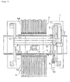
- Fig.1 and Fig.2 show the overall structure of a component mounting machine, an embodiment of this invention.
- a conveyer 2 for conveying printed substrates is installed on the base 1, the printed substrate is conveyed on the conveyer 2, and is brought to a stop at a predetermined component mounting position.
- Each tape feeder 4a is adapted for sending out a tape holding and containing chip components 20 such as ICs, transisters, condensers, etc., at regular intervals from a reel, and is provided with a ratchet type feeder mechanism incorporated at the tape send-out end so that the feeder tape 4a may be intermittently sent out as chip components are picked up by a head unit 5 to be described later.
- chip components 20 such as ICs, transisters, condensers, etc.
- the head unit 5 adapted for moving both in the X axis direction (direction of the conveyer 2) and in the Y axis direction (direction perpendiclar to the X axis direction on a horizontal plane) is installed above the base 1.
- a head unit support member 11 is supported on the fixed rails 7, and a nut portion 12 provided on the support member 11 is in screw-engagement with the call screw 8.
- the supporting member 11 is provided with a guide member 13 extended in the X-axis direction and a ball screw 14 to be rotated by an X axis servomotor 15, a head unit 5 is movably supported by the guide member 13, and a nut portion (not shown) provided in this head unit 5 is in screw-engagement with the ball screw 14.
- the ball screw 8 is rotated by the operation of the Y axis servomotor 9 and the support member 11 is moved in the Y axis direction
- the ball screw 14 is rotated by the operation of the X axis servomotor 15 and the head unit 5 is moved in the X axis direction relative to the support member 11.
- the Y axis servomotor 9 and X axis servomotor 15 are respectively provided with position detecting means 10 and 16 each constituted of an encoder.
- the head unit 5 is provided with a plurality of attracting nozzles and driving means for vertically transferring and rotating each attracting nozzle. As shown also in Fig. 3, this embodiment is provided, on the head unit 5, with first and second attracting nozzles 21 and 22, two Z-axis servomotors as driving means for vertically transferring each attracting nozzle 21,22, and two R-axis servomotors as driving means for rotating each attracting nozzle 21,22.
- the attracting nozzles 221,22 are installed on the lower ends of their hollow nozzle shafts 21a,22a, the nozzle shafts 21a,22a are mounted on their respective housings (not shown) in a state capable of vertically sliding but incapable of rotating relative to each other, and each housing is rotatably held on the frame of the head unit 5; thus, each attracting nozzle 21,22 is made capable of transferring in the Z-axis (vertical) direction and rotating about the R-axis (nozzle axis). Further, each nozzle shaft 21a,22a is driven in the Z-axis direction by each Z-axis servomotor 23,24 through transmission means (not shown), and each housing above is driven for rotation by each R-axis servomotor through transmission means (not shown).
- the servomotors above 23 through 26 are provided with position detecting means 27 through 30, respectively.
- Each nozzle shaft 21a,22a is connected to negative pressure supplying means (not shown) through valves, etc., so that the negative pressure for component attraction is supplied when required.
- a laser unit 31 As optical detecting means for detecting the projections of the chip components K1,K2 attracted to the attracting nozzles 21,22.
- This laser unit 31 has a laser generating section (parallel light beam emitting section) 31a and a detector (light receiving section) 31b, and this laser generating section 31a and the detector 31b are disposed opposite to each other on both sides of a space in which the chip components K1 and K2 attracted to the attracting nozzles 21 and 22 are located while being recognized.
- the detector 31b is constituted of a CCD.
- the attracting nozzles 21 and 22 are disposed aslant relative to the laser emitting direction and are spaced apart by a predetermined distance, so that the projections of the chip components K1 and K2 attracted to the attracting nozzles 21 and 22 do not overlap with each other.
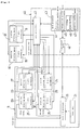
- Fig.5 shows an embodiment of the control system.
- the component mounting machine is provided with a main controller 40, which is provided with an axis controller (driver) 41, input/output means 42, and a main processor 43.
- axis controller driver
- main processor 43 main processor
- the Y-axis servomotor 9, X-axis servomotor 15, Z-axis servomotors 23,24 for attracting nozzles 21,22 of the head unit 5, R-axis servomotors 25,26, and position detecting means 10,16,27 through 30 provided for these servomotors are electrically connected to the axis controller 41 of the main controller 40.
- the operations of the servomotors 9, 15 and 23 through 26 are controlled by this axis controller 41.
- the laser unit 31 is electrically connected to the laser unit processor (calculation processing means) 35 so that the calculation process of the component recognizing informations such as the component projection width, nozzle rotation angle, etc., are carried out by this laser unit processor 35 on the basis of outputs of the laser unit 31 and position detecting means 29,30.
- This laser unit processor 35 is connected to the main processor 43 through the input/output means 42 of the main processor 40.
- it is difficult for the laser unit processor 35 because of its capability, to start calculation of the projection width of another chip component while calculating the projection width, etc., of a component (that is, to carry out respective calculations partly in overlap with each other), and it is required to carry out calculations for respective chip components in their perfectly lagged period.
- Such a laser unit processor 35 is what is generally used in this kind of recognizing system.
- the main processor 43 controls the operations of the servomotors 9, 15, 23 through 26 through the axis controller 41 so that the chip component is automatically attracted, recognized and mounted, and carries out processes such as reading the informations from the laser unit processor 35 through the input/output means 42. Since this main processor 43 controls according to such a program as shown in the flow chart (to be described later), it will functionally include the attraction control means 44, recognition control means 45, timing adjusting means 46 and mounting control means 47.
- the attraction control means 44 controls the operations of the head unit 5 and the attracting nozzles 21 and 22 so that they attract chip components from the tape feeder 4a of the component feeding section 4, and, in this embodiment, makes the attracting nozzles 21 and 22 attract chip compoents successively.
- the recognition control means 45 carries out, for each of the components K1 and K2 attracted to each attracting nozzle 21 and 22, the component recognition process including the process of actuating the R-axis servomotors 25 and 26 to rotate the attracting nozzles 21 and 22 after the components are attracted and the process of recognizing the chip component attracting state on the basis of the informations obtained from the laser unit processor 35 while rotating the attracting nozzles.
- the process of recognizing the chip component attracting state on the basis of the informations obtained from the laser unit 35 is carried out while rotating the attracting nozzles in the sense for recognition after the preliminary rotation process in which the attracting nozzles are rotated in a sense contrary to that for recognition is carried out.
- the timing adjusting means 46 adjust the timing of the component recognition process so that the period of the component recognition process for the component attracted to one attracting nozzle at least partly overlap with the period of the component recognition process for the component attracted to the other attracting nozzle; in this embodiment, while the component recognition process is being carried out for the component attracted to the first attracting nozzle 21, the preliminary rotation of the component already attracted to the second attracting nozzle 22 is started.
- the mounting control means 37 controls the operations of the head unit 5 and attracting nozzles 21 and 22 so that chip component is mounted at the predetermined position on the printed substrate.
- each attracting nozzle 21,22 is supplied with attracting negative pressure at the step S1, and a chip component K1 is attracted to the first attracting nozzle 21 at the step S2.
- the head unit 5 is transferred to above the component feeding section 4; when the head unit 5 reaches the position where the attracting nozzle 21 corresponds to the tape feeder 4a, the attacting nozzle 21 is lowered and attracts the chip component K1.
- the first attracting nozzle 21 is raised up to a predetermined recognition height corresponding to the laser unit 31, and the preliminary rotation of the first attracting nozzle 21 is started.
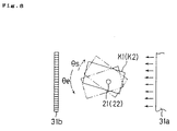
- the attracting nozzle 21 attracting a chip component K1 is rotated by a definite angle ⁇ s in a sense contrary to that for recognition rotation (clockwise in Fig.8) as shown with dash-and-single-dotted lines.
- a state of the chip component K1 is securely obtained in which its longer side is inclined toward a definite side relative to the laser beam direction, and this state is taken as the initial position for carrying out the main recognition process.
- step S4 it is judged whether the preliminary rotation of the first attracting nozzle 21 is completed or not.
- the operation proceeds to the step S5, and the main recognition process for the chip component K1 atttracted to the first attracting nozzle 21 is carried out as described in detail later.
- the attracting operation by the second attracting nozzle 22 is carried out at the step S7 in the same manner as the attracting operation by the first attracting nozzle 21, and, when this attracting operation is completed, at the step S8, the second attracting nozzle 22 is raised up to a predetermined recognition height corresponding to the laser unit 31, and the preliminary rotation of the second attracting nozzle 22 (the same as the preliminary rotation of the first attracting nozzle 21) is started.
- the attracting operation and the preliminary rotation of the second attracting nozzle 22 are carried out in parallel with the steps S3 through S5 on the first attracting nozzle 21 side.
- step S9 it is judged whether the preliminary rotation of the second attracting nozzle 22 is completed or not.
- step S10 it is judged whether the recognition of the chip component K1 attracted to the attracting nozzle 21 (process at the step S4 above) is completed or not.
- the operation proceeds to the step S11, and the main recognition process for the chip component K2 atttracted to the second attracting nozzle 22 is carried out as described in detail later.
- the chip component K1 is mounted at the step S6. Practically, by transferring the head unit 5 to the target position above the printed substrate 3, lowering the first attracting nozzle 21 and intercepting the negative pressure supply, the chip component K1 is mounted on the printed substrate 3.
- step S12 it is judged whether the mounting operation of the chip component K1 by the attracting nozzle 21 is completed or not, then, when completed, the operation proceeds to the step S13, and the mounting operation of the chip component K2 by the second attracting nozzle 22 (the same as the mounting operation by the first attracting nozzle 21) is carried out.
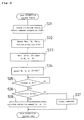
- Fig.7 is a flow chart showing the routine of the main recognition process to be carried out at each of the steps S5 and S11 above.
- the projection width Ws, center position Cs and rotation angle ⁇ s of the chip component at the instance when the preliminary rotation above is completed are detected.
- the attracting nozzle is rotated from its initial position shown in Fig.8 with dash-and-double-dotted lines in the predetermined direction for the recognition rotation (anticlockwise in Fig.8) by a definite angle ⁇ e, and, while the attracting nozzle is being thus rotated, the projection width W of the chip component is detected repeatedly (steps S22, S23).
- This chip component projection width W is given by the calculation at the laser unit processor 35 on the basis of the output of the laser unit 31.
- the center position Cm and the rotation angle ⁇ m (rotation angle referred to the position before the preliminary rotation) are detected. That is, while the chip component attracted to the attracting nozzle is being rotated, the projection width becomes minimum when the longer side of the chip component is directed in the same direction as the laser beam direction, and the projection width Wmin (corresponding to the length of the shorter side of the chip component), center position Cm and the rotation angle ⁇ m at this instance are detected.
- the attraction is judged to be normal if, for example, the value corresponding to the component shorter side length obtained from the projection width Wmin above and the value corresponding to the component longer side length obtained by calculation from the above or other data are sufficiently approximate to the actual lengths of the shorter and longer sides of the chip component and the rotation angle ⁇ m is in the predetermined range, and is judged to be defective if not.
- the operation proceeds to the step S26 and the chip component concerned is disused; when the attraction is normal, the operation proceeds to the step S27.
- the length of the chip component shorter side, the deviation of the component center from the nozzle center in the shorter side direction and the rotation angle deviation are obtained from the projection width Wmin above, center position Cm and the rotation angle ⁇ m. Further, from these and other data, the length of the component longer side and the deviation of the component center from the nozzle center in the longer side direction are obtained by calculation, and from these are calculated the mounting position correction amounts Xc, Yc and ⁇ c.
- the target mounting position is corrected by these correction amounts Xc, Yc and ⁇ c.
- the length of one side (shorter side) of the attracted component is obtained from the minumum projection width Wmin while the length of the other side (longer side) is obtained by calculation in an example of the main recognition process shown in Fig.7
- the lengths of the longer and shorter sides may be obtained both from the detected projection width as shown in Fig.9 as another example of the main recognition process.
- the projection width W of the chip component is detected. Then, the rotational position at which the projection width becomes minimum is obtained, the projection width Wmin, component center position Cm and the rotation angle ⁇ m (rotation angle referred to the position before the preliminary rotation) at that instance are detected at the step S32, and the projection width Wmin above, the difference (Cm-Cn) between the component center position Cm and the nozzle center position Cn above, and the rotation angle ⁇ m above are taken as the projection width Wy corresponding to the component shorter side length, positional deviation Yc in the Y axis direction and the rotation angle deviation ⁇ c, respectively, at the step S33.
- the projection width and the component center position at the instance when the attracting nozzle is rotated up to the rotation angle of ( ⁇ c + 90° ) are detected, and the projection width above and the difference between the component center position and the nozzle center position are taken as the projection width Wx corresponding to the component longer side length, and the positional deviation Xc in the X-axis direction, respectively, at the step S34.
- the attraction is judged to be normal or not at the step S36 in the same manner as at the step S25 in Fig.7, and, if not normal, the chip component is disused at the step S37.
- correction amounts are obtained with the Y-axis direction positional deviation Yc, rotational angle deviation ⁇ c and the X axis direction positional deviation Xc above at the step S38.
- the time chart for the attracting operation using the attracting nozzles 21 and 22, component recognition process and mounting operation is as shown in Fig.10.
- A, B, B1, B2, C, and W indicate the period for attracting operation, component recognition process, preliminary rotation in the component recognition process, main recognition precess in the component recognition process, and mounting operation, respectively.
- the attracting operation for the chip component K1, the recognition process B of the chip component K1 including the preliminary rotation B1 and the main recognition process B2, and the mounting operation C1 for the chip component K1 are carried out in succession.
- the attracting operation A is started after the attracting operation on the first nozzle side is completed.
- the attracting operation A and preliminary rotation B1, main recognition process B2 and mounting operation C for the chip component K2 are carried out in succession also on this second nozzle side, the attracting operation A and the preliminary rotation B1 among them are carried out in time overlap with the recognition process on the first nozzle side. Further, if the recognition process B on the first nozzle side is not yet completed when the preliminary rotation B1 on the second nozzle side is completed, the main recognition process B2 and the mounting operation C on the second nozzle side are carried out after a lapse of waiting period W until the recognition process B on the first nozzle side is completed.
- the chip component K1 at the start of the main recognition process is surely in a state inclined toward a definite side relative to the laser beam. Therefore, the minimum projection width Wmin can be surely detected while the attracting nozzle is rotated by a definite angle ⁇ e during the main recognition process, and the component attracting state can be recognized rapidly and accurately.
- the laser unit processor 35 is not capable of calculating the projection widths, etc., for a plurality of components in partial overlap with each other, since it is not required to calculate the projection widths, etc., during the preliminary rotation above, even if the period of preliminary rotation on the second attracting nozzle side overlaps with that of the recognition process on the first attracting nozzle side, there is no trouble for the calculation at the laser unit processor 35 if the main recognition processes does not overlap with each other.
- the period of waiting W on the second nozzle side becomes shorter than that in the former case (see Fig.12), the time loss during the mounting operation from attraction to mounting is reduced and the mounting time is shortened.
- the attracting operations of the attracting nozzles 21 and 22 in the embodiment above are so controlled, as an example for the case where simultaneous attractions are difficult, that the attraction by the second nozzle 22 is carried out after the attraction by the first nozzle 21 is completed, simultaneous attractions may be possible according the the positional relation between the attracting nozzles 21,22 and the tape feeder 4a of the component feeder section 4. In such a case, the attracting operation may be controlled as shown in the flow chart of Fig.11.
- both attracting nozzles 21,22 are supplied with attracting negative pressure at the step S101, the attraction of the component K1 by the first attracting nozzle 21 (step S102) and the attraction of the component K2 by the second attracting nozzle 22 (step S107) are simultaneously carried out in parallel, and both attracting nozzles are raised and preliminarily rotated in parallel (steps S103 and S108).
- step S104 the judgement of completion of the preliminary rotation on the first nozzle side (step S104), and the main recognition process (step S105) and mounting operation (step S106) of the chip component K1
- step S109 the judgement of completion of recogintion process of the chip component K1
- step S111 the main recognition process of the chip component K2
- step S112 judgement of completion of mounting operation of the chip component K1
- step S113 the mounting operation of the chip component K2
- This embodiment also, since the preliminary rotation in the recognition process on the second attracting nozzle is carried out while the recognition process on the second attracting nozzle side is being carried out, the time loss is reduced.
- This embodiment is further advantageous for shortening the mounting time because attractions are carried out simultaneously by a plurality of attracting nozzles.
- both component recognition processes on the first nozzle side and on the second nozzle side may be overlapped with each other with their main recognition processes included.
- the number of attracting nozzles equipped on the head unit 5 may be three or more.
- a chip component mounting machine having a head unit provided with a plurality of attracting nozzles, since it is provided with optical detecting means for detecting the projections of the chip components attracted to the attracting nozzles,calculatig means for calculating the projection width of the chip component attracted to the attracting nozzle on the basis of the output of the optical detecting means,recognition control means for rotating the attracting nozzle attracting a chip component and carrying out the chip component recognition process for the chip component attracted to each attracting nozzle on the basis of the information obtained from the calculating means during the rotation of the attracting nozzle, and timing adjusting means for adjusting the timings of component recognition processes so that the periods of the component recognition processes for components attracted to respective attracting nozzles at least partly overlap with each other, the time lag between the component recognition processes for the components of respective attracting nozzles becomes smaller. Therefore, the time loss during the mounting operation can be reduced and the mounting time can be shortened.
- the main recognition process for recognizing the chip component attracting state is carried out while rotating the attracting nozzle in the sense for recognition after carrying out the preliminary rotation in which the attracting nozzle is rotated by a predetermined angle in a sense contrary to the predetermined sense for recognition rotation, and the timing is so adjusted by the timing adjusting means above that, while the component recognition process for one attracting nozzle is being carried out, the preliminary rotation in the component recognition process for the attracting component of the other attracting nozzle is carried out.
- the main recognition process can be carried out rapidly and accurately due to the preliminary rotation above.
- the time lag between the component recognition processes for attracting components of the resp ective attracting nozzles can be made smaller and the mounting time can be shortened within a range not causing a trouble.
Abstract
Description
- The present invention relates to a method for mounting components at specific positions, especially chip components onto a substrate such as a printed circuit board, comprising the steps of picking up the components through attracting nozzle units, transferring the components and placing the same in a detection area of an optical detecting means emitting light beams for detecting a projected width of the component, subjecting the components to a recognition process each, for recognizing the components and/or their positions relative to the attracting nozzle units, said recognition process including a preliminary rotation of the components and a main recognition process wherein projected width data are obtained under rotation of the component, and mounting the components at the desired positions.
- The present invention relates also to a mounting device for mounting components at specific positions, especially chip components onto a substrate such as a printed circuit board, comprising a moveable mounting head unit having a plurality of attracting nozzle units for picking up components from a component supply unit, an optical detecting means emitting light beams for detecting a projected width of said components, a control unit for controlling the mounting head unit including recognition control means for controlling recognition processes for recognizing the components and/or the positions thereof relative to the attracting nozzle units.
- So far has been generally known a chip component mounting machine on which a chip component such as electronic component like IC, etc., is attracted from the component feeding section by a chip component mounting head unit, transferred to a positioned printed substrate and mounted at a predetermined position on the printed substrate. This mounting machine usually has a head unit adapted for moving in the X axis and Y axis directions and an attracting nozzle adapted for moving in the Z axis direction and rotatable, and is provided with driving means for movement in various directions and for rotation. By controlling these driving means and negative pressure supplying means for the attacting nozzle by the controller section, the chip component is automatically attracted and mounted.
- On such a mounting machine, the position of the component as attracted to the attracting nozzle has some degree of dispersion, and it is required to correct the mounting position acccording to the positional deviation of the component.
- Therefore, as disclosed in Japanese Unexamined Patent Publication Hei4-322924, an apparatus has been known in which the head unit is provided with an optical detecting means composed of a parallel light beam emitting section and a light receiving section located opposite to each other on both sides of a domain through which the attracting nozzles are raised and lowered so that the projection of the chip component attracted to the attracting nozzle is detected and the chip component attracting state is recognized on the basis of this detection.
- That is, as the component recognizing process, this apparatus detects the projection of the chip component (the range in which the parallel light beams are intercepted by the chip component) attracted to the attracting nozzle and positioned between the light beam emitting section and the light receiving section of the optical detecting means while rotating the attracting nozzle, and, on the basis of this detection data, obtains the values corresponding to the widths of the shorter side and the longer side of the chip component by examining the rotational position at which the projection width becomes a minimum and calculating the minimum value. The chip component attracting state is judged to be normal or not on the basis of the comparison of this value with the actual chip size, and, if normal, the positional deviation of the chip component center position is calculated and the mounting position correction is obtained from the detection data above.
- Hereupon, although the head unit for the apparatus disclosed in the patent publication above is provided with only one attracting nozzle, apparatus has been proposed, to improve the mounting efficiency, whose head unit is provided with a plurality of attracting nozzles so that each attracting nozzle can attract and mount the respective component.
- When a plurality of attracting nozzles are provided as described above and the chip component attracting state of each attracting nozzle is examined by the component recognition using the optical detecting means above, the component recognition process for each attracted component has been so far started with some time lag so that the projection widths, etc., above can be easily calculated.
- This process is shown in Fig.12 as a time chart for the case where the head unit is provided with two attracting nozzles. On the first attracting nozzle side, the attraction of a chip component, the component recognition by means of the optical detecting means above, and the mounting of the component are carried out successively. On the other hand, the attraction by the second attracting nozzle is started after the completion of the attraction by the first attracting nozzle, and the component attraction and component recognition are carried out successively also on the second attracting nozzle side. However, the component recognition on the second attracting nozzle side is started with a time lag after the completion of component recognition on the first attracting nozzle side; that is, in the case where the component is still being recognized on the first attracting nozzle side when the attraction on the second attracting nozzle side is completed, the start of the component recognition on the second attracting nozzle side is retarded until the component recognition is completed on the first attracting nozzle side.
- Therefore, a waiting period for time adjustment is produced between the attracting motion and the component recognition on the second attracting nozzle side, and, as the component recognition becomes longer on the first attracting nozzle side, this waiting period also becomes longer, which produces a time loss during the mouting time from attraction to mounting preventing desirable reduction of the mounting time.
- It is therefore an objective of the present invention to provide an improved method and an improved mounting device of the afore-indicated type which allow an improved component recognition so as to shorten the components mounting time by reducing the time lag between the recognition processes of respective attracted components.
- As regards the method, the afore-mentioned objective is performed, according to the present invention, in that the timing of the recognition processes for a plurality of components is adjusted by a timing adjusting means in response to each other, such that a recognition process for a first component overlaps at least partly a recognition process for another component.
- Accordingly, the time lag between component recognitions at the respective attracting nozzles becomes smaller and the waiting time for time adjustments becomes shorter.
- According to a preferred embodiment of the invention, the timing is adjusted in such a manner that while the recognition process for said first component is carried out, the preliminary rotation of at least another component is performed.
- According to a further preferred embodiment, the timing of the main recognition processes for a plurality of components is adjusted such that said main recognition processes are performed in succession, said main recognition processes are not overlapping each other.
- Accordingly, since a main recognition process of a first component merely overlaps the preliminary rotation of one or several other components and does not overlap other main recognition processes of other components, the time lag between component recognitions can be reduced, but the processing capacity of the calculating mean for calculating the projection width data can be relatively small, as the main recognition processes are performed in succession.
- As regards the apparatus, the afore-mentioned objective is performed, according to the present invention, in that the control unit includes timing adjusting means for adjusting the timing of the recognition processes for a plurality of components in response to each other such that said recognition processes overlap each other at least partially.
- According to a preferred embodiment, said timing adjusting means is adapted to adjust the timing of the recognition processes such that while the recognition process for a first component is performed, the preliminary rotation of at least another component is carried out.
- According to a further preferred embodiment, the timing adjusting means is adapted to adjust the timing of a plurality of main recognition processes for a plurality of components such that the same are performed in succession.
- The mounting device is therefore advantageous in that it can considerably reduce the component recognition period with a relatively small processing capacity of the control unit.
- Further preferred embodiments of the present invention are laid down in further dependent claims.
- Hereinafter, the present invention is illustrated and explained in greater detail by means of a preferred embodiment thereof in connection with accompanying drawings, wherein:
- Figure 1 is a schematic plan view showing a chip component mounting machine having a component recognizing apparatus according to a preferred embodiment of this invention,
- Figure 2 is a schematic front view of the chip component mounting machine according to figure 1,
- Figure 3 is a front view showing the principal portions of a head unit of the component mounting machine according to figure 1, said head unit including two attracting nozzles for attracting components,
- Figure 4 is a schematic plan view of a laser unit for detecting components, said laser unit being provided on the head unit shown in figure 1,
- Figure 5 is a block diagram showing the control system of the chip component mounting machine according to figure 1,
- Figure 6 is a flow chart showing an example of the control of the mounting operation performed by the mounting machine according to figure 1,
- Figure 7 is a flow chart showing the routine of a main recognition process in the control of the mounting operation carried out by the component mounting machine according to figure 1,
- Figure 8 is an explanatory view showing the rotating operation of the chip component during the component recognition process, said component being placed in a detection area of the laser unit shown in figure 4,
- Figure 9 is a flow chart showing another example of the routine of the main recognition process in the control of the mounting operation carried out by the mounting machine according to figure 1,
- Figure 10 is a time chart showing the timing of the mounting operations including an attracting operation and the recognition process for two components attracted to two attracting nozzles,
- Figure 11 is a flow chart showing an example of the control of the mounting operation,
- Figure 12 is a time chart showing the time relation of the attracting operation, component recognition process and mounting operation based on the prior art.
- Fig.1 and Fig.2 show the overall structure of a component mounting machine, an embodiment of this invention. As shown, a
conveyer 2 for conveying printed substrates is installed on the base 1, the printed substrate is conveyed on theconveyer 2, and is brought to a stop at a predetermined component mounting position. - On the sides of the
conveyer 2 are disposed component feeding sections 4 each provided with many rows oftape feeders 4a. Eachtape feeder 4a is adapted for sending out a tape holding and containing chip components 20 such as ICs, transisters, condensers, etc., at regular intervals from a reel, and is provided with a ratchet type feeder mechanism incorporated at the tape send-out end so that thefeeder tape 4a may be intermittently sent out as chip components are picked up by ahead unit 5 to be described later. - The
head unit 5 adapted for moving both in the X axis direction (direction of the conveyer 2) and in the Y axis direction (direction perpendiclar to the X axis direction on a horizontal plane) is installed above the base 1. - That is, while a pair of
fixed rails 7 extended in the Y axis direction and a ball screw 8 to be rotated by aY axis servomotor 9 are disposed on the base 1, a headunit support member 11 is supported on thefixed rails 7, and anut portion 12 provided on thesupport member 11 is in screw-engagement with the call screw 8. The supportingmember 11 is provided with aguide member 13 extended in the X-axis direction and aball screw 14 to be rotated by anX axis servomotor 15, ahead unit 5 is movably supported by theguide member 13, and a nut portion (not shown) provided in thishead unit 5 is in screw-engagement with theball screw 14. While the ball screw 8 is rotated by the operation of theY axis servomotor 9 and thesupport member 11 is moved in the Y axis direction, theball screw 14 is rotated by the operation of theX axis servomotor 15 and thehead unit 5 is moved in the X axis direction relative to thesupport member 11. - The
Y axis servomotor 9 andX axis servomotor 15 are respectively provided with position detecting means 10 and 16 each constituted of an encoder. - The
head unit 5 is provided with a plurality of attracting nozzles and driving means for vertically transferring and rotating each attracting nozzle. As shown also in Fig. 3, this embodiment is provided, on thehead unit 5, with first and second attractingnozzles nozzle nozzle - The attracting
nozzles 221,22 are installed on the lower ends of theirhollow nozzle shafts nozzle shafts head unit 5; thus, each attractingnozzle nozzle shaft axis servomotor - The servomotors above 23 through 26 are provided with position detecting means 27 through 30, respectively. Each
nozzle shaft - On the lower end portion of the
head unit 5 is disposed alaser unit 31 as optical detecting means for detecting the projections of the chip components K1,K2 attracted to the attractingnozzles laser unit 31 has a laser generating section (parallel light beam emitting section) 31a and a detector (light receiving section) 31b, and thislaser generating section 31a and thedetector 31b are disposed opposite to each other on both sides of a space in which the chip components K1 and K2 attracted to the attractingnozzles detector 31b is constituted of a CCD. - The attracting
nozzles nozzles - Fig.5 shows an embodiment of the control system. In this diagram, the component mounting machine is provided with a
main controller 40, which is provided with an axis controller (driver) 41, input/output means 42, and amain processor 43. - The Y-
axis servomotor 9,X-axis servomotor 15, Z-axis servomotors nozzles head unit 5, R-axis servomotors axis controller 41 of themain controller 40. The operations of theservomotors axis controller 41. - The
laser unit 31 is electrically connected to the laser unit processor (calculation processing means) 35 so that the calculation process of the component recognizing informations such as the component projection width, nozzle rotation angle, etc., are carried out by thislaser unit processor 35 on the basis of outputs of thelaser unit 31 and position detecting means 29,30. Thislaser unit processor 35 is connected to themain processor 43 through the input/output means 42 of themain processor 40. In this embodiment, it is difficult for thelaser unit processor 35, because of its capability, to start calculation of the projection width of another chip component while calculating the projection width, etc., of a component (that is, to carry out respective calculations partly in overlap with each other), and it is required to carry out calculations for respective chip components in their perfectly lagged period. Such alaser unit processor 35 is what is generally used in this kind of recognizing system. - The
main processor 43 controls the operations of theservomotors axis controller 41 so that the chip component is automatically attracted, recognized and mounted, and carries out processes such as reading the informations from thelaser unit processor 35 through the input/output means 42. Since thismain processor 43 controls according to such a program as shown in the flow chart (to be described later), it will functionally include the attraction control means 44, recognition control means 45, timing adjusting means 46 and mounting control means 47. - That is, the attraction control means 44 controls the operations of the
head unit 5 and the attractingnozzles tape feeder 4a of the component feeding section 4, and, in this embodiment, makes the attractingnozzles - The recognition control means 45 carries out, for each of the components K1 and K2 attracted to each attracting
nozzle axis servomotors nozzles laser unit processor 35 while rotating the attracting nozzles. In this embodiment, as the component recognition process, the process of recognizing the chip component attracting state on the basis of the informations obtained from thelaser unit 35 is carried out while rotating the attracting nozzles in the sense for recognition after the preliminary rotation process in which the attracting nozzles are rotated in a sense contrary to that for recognition is carried out. - The timing adjusting means 46 adjust the timing of the component recognition process so that the period of the component recognition process for the component attracted to one attracting nozzle at least partly overlap with the period of the component recognition process for the component attracted to the other attracting nozzle; in this embodiment, while the component recognition process is being carried out for the component attracted to the first attracting
nozzle 21, the preliminary rotation of the component already attracted to the second attractingnozzle 22 is started. - The mounting control means 37 controls the operations of the
head unit 5 and attractingnozzles - An example of controls by the
main controller 40 is described practically referring to the flow charts shown in Figs.6 and 7. In the following description for the flow charts, the preliminary rotation and the main recognition operation are described assuming that the chip component is oblong, and the chip component as attracted and the laser unit are in a positional relation that the longer side of the chip component is generally parallel to the laser beam within a definite rotation angle error. However, the shorter side and the longer side of the chip component may be positioned contrariwise, or may be two sides of a generally square chip component. - As seen in Fig.6, when the mounting operation is started, each attracting
nozzle nozzle 21 at the step S2. Describing more practically, in this attracting operation, thehead unit 5 is transferred to above the component feeding section 4; when thehead unit 5 reaches the position where the attractingnozzle 21 corresponds to thetape feeder 4a, theattacting nozzle 21 is lowered and attracts the chip component K1. - When the attracting operation by the first attracting
nizzle 21 is completed, at the step S3, the first attractingnozzle 21 is raised up to a predetermined recognition height corresponding to thelaser unit 31, and the preliminary rotation of the first attractingnozzle 21 is started. Practically saying, by this preliminary rotation, as shown in Fig.8, the attractingnozzle 21 attracting a chip component K1 is rotated by a definite angle ϑs in a sense contrary to that for recognition rotation (clockwise in Fig.8) as shown with dash-and-single-dotted lines. By this preliminary rotation, a state of the chip component K1 is securely obtained in which its longer side is inclined toward a definite side relative to the laser beam direction, and this state is taken as the initial position for carrying out the main recognition process. - In succession, at the step S4, it is judged whether the preliminary rotation of the first attracting
nozzle 21 is completed or not. When the preliminary rotation is completed, the operation proceeds to the step S5, and the main recognition process for the chip component K1 atttracted to the first attractingnozzle 21 is carried out as described in detail later. - On the other hand, after the completion of the attracting operation by the first attracting
nozzle 21, the attracting operation by the second attractingnozzle 22 is carried out at the step S7 in the same manner as the attracting operation by the first attractingnozzle 21, and, when this attracting operation is completed, at the step S8, the second attractingnozzle 22 is raised up to a predetermined recognition height corresponding to thelaser unit 31, and the preliminary rotation of the second attracting nozzle 22 (the same as the preliminary rotation of the first attracting nozzle 21) is started. The attracting operation and the preliminary rotation of the second attractingnozzle 22 are carried out in parallel with the steps S3 through S5 on the first attractingnozzle 21 side. - Then, at the step S9, it is judged whether the preliminary rotation of the second attracting
nozzle 22 is completed or not. When this preliminary rotation is completed, at the step S10, it is judged whether the recognition of the chip component K1 attracted to the attracting nozzle 21 (process at the step S4 above) is completed or not. When it is judged that the recognition of the chip component K1 is completed, the operation proceeds to the step S11, and the main recognition process for the chip component K2 atttracted to the second attractingnozzle 22 is carried out as described in detail later. - As the process after the main recognition process (step S5) on the first attracting
nozzle 21 side, the chip component K1 is mounted at the step S6. Practically, by transferring thehead unit 5 to the target position above the printedsubstrate 3, lowering the first attractingnozzle 21 and intercepting the negative pressure supply, the chip component K1 is mounted on the printedsubstrate 3. On the other hand, as the processes after the main recognition process (step S11) on the second attractingnozzle 22 side, at the step S12, it is judged whether the mounting operation of the chip component K1 by the attractingnozzle 21 is completed or not, then, when completed, the operation proceeds to the step S13, and the mounting operation of the chip component K2 by the second attracting nozzle 22 (the same as the mounting operation by the first attracting nozzle 21) is carried out. - Fig.7 is a flow chart showing the routine of the main recognition process to be carried out at each of the steps S5 and S11 above. At the step S21 in this routine, the projection width Ws, center position Cs and rotation angle ϑs of the chip component at the instance when the preliminary rotation above is completed are detected. In succession, the attracting nozzle is rotated from its initial position shown in Fig.8 with dash-and-double-dotted lines in the predetermined direction for the recognition rotation (anticlockwise in Fig.8) by a definite angle ϑe, and, while the attracting nozzle is being thus rotated, the projection width W of the chip component is detected repeatedly (steps S22, S23). This chip component projection width W is given by the calculation at the
laser unit processor 35 on the basis of the output of thelaser unit 31. - At the step S24, while the minimum projection width Wmin is obtained from the data of the projection width W above, the center position Cm and the rotation angle ϑm (rotation angle referred to the position before the preliminary rotation) are detected. That is, while the chip component attracted to the attracting nozzle is being rotated, the projection width becomes minimum when the longer side of the chip component is directed in the same direction as the laser beam direction, and the projection width Wmin (corresponding to the length of the shorter side of the chip component), center position Cm and the rotation angle ϑm at this instance are detected.
- In succession, at the step S25, it is judged on the basis of the data above, etc., whether the component attraction is normal or not. Here, the attraction is judged to be normal if, for example, the value corresponding to the component shorter side length obtained from the projection width Wmin above and the value corresponding to the component longer side length obtained by calculation from the above or other data are sufficiently approximate to the actual lengths of the shorter and longer sides of the chip component and the rotation angle ϑm is in the predetermined range, and is judged to be defective if not. When not normal (when the attraction is defective), the operation proceeds to the step S26 and the chip component concerned is disused; when the attraction is normal, the operation proceeds to the step S27. At the step S27, the length of the chip component shorter side, the deviation of the component center from the nozzle center in the shorter side direction and the rotation angle deviation are obtained from the projection width Wmin above, center position Cm and the rotation angle ϑm. Further, from these and other data, the length of the component longer side and the deviation of the component center from the nozzle center in the longer side direction are obtained by calculation, and from these are calculated the mounting position correction amounts Xc, Yc and ϑc. When the chip component is mounted at the step S6 or S13 in Fig.6, the target mounting position is corrected by these correction amounts Xc, Yc and ϑc.
- Although the length of one side (shorter side) of the attracted component is obtained from the minumum projection width Wmin while the length of the other side (longer side) is obtained by calculation in an example of the main recognition process shown in Fig.7, the lengths of the longer and shorter sides may be obtained both from the detected projection width as shown in Fig.9 as another example of the main recognition process.
- The process of Fig.9 is described hereafter. After the preliminary rotation, while the attracting nozzle is being rotated in the component recognition direction at the step S31, the projection width W of the chip component is detected. Then, the rotational position at which the projection width becomes minimum is obtained, the projection width Wmin, component center position Cm and the rotation angle ϑm (rotation angle referred to the position before the preliminary rotation) at that instance are detected at the step S32, and the projection width Wmin above, the difference (Cm-Cn) between the component center position Cm and the nozzle center position Cn above, and the rotation angle ϑm above are taken as the projection width Wy corresponding to the component shorter side length, positional deviation Yc in the Y axis direction and the rotation angle deviation ϑc, respectively, at the step S33.
- Next, the projection width and the component center position at the instance when the attracting nozzle is rotated up to the rotation angle of ( ϑc + 90° ) are detected, and the projection width above and the difference between the component center position and the nozzle center position are taken as the projection width Wx corresponding to the component longer side length, and the positional deviation Xc in the X-axis direction, respectively, at the step S34. Then, after the attracting nozzle is rotated at the step S35 up to a set rotation angle ϑf which makes such detections possible, the attraction is judged to be normal or not at the step S36 in the same manner as at the step S25 in Fig.7, and, if not normal, the chip component is disused at the step S37. When the attraction is normal, correction amounts are obtained with the Y-axis direction positional deviation Yc, rotational angle deviation ϑc and the X axis direction positional deviation Xc above at the step S38.
- Comparing the case according to the example of Fig.7 with the case according to the example of Fig.9, when the chip component is smaller, since the error of the calculated value may become larger when the chip component longer side length is obtained by calculation as in Fig.7 due to errors included in the data for the calculation, higher accuracy is obtained when both side lengths are obtained by projection width detection as shown in Fig.9. On the other hand, when the chip component is larger, since a larger positional deviation of the component may happen during its rotation if the component is rapidly rotated through a large rotation angle, the method in which the attracting nozzle rotation angle for the projection width detection is made smaller and the chip component longer side length is obtained by calculation as shown in Fig.7 is advantageous for the accuracy. Therefore, it is effective to selectively employ the process as shown in Fig.7 or the process as shown in Fig.9 according to the kind of chip components.
- When employing such apparatus as described above, the time chart for the attracting operation using the attracting
nozzles - As shown in this time chart, on the first nozzle side, the attracting operation for the chip component K1, the recognition process B of the chip component K1 including the preliminary rotation B1 and the main recognition process B2, and the mounting operation C1 for the chip component K1 are carried out in succession.
- On the second nozzle side, the attracting operation A is started after the attracting operation on the first nozzle side is completed. Although the attracting operation A and preliminary rotation B1, main recognition process B2 and mounting operation C for the chip component K2 are carried out in succession also on this second nozzle side, the attracting operation A and the preliminary rotation B1 among them are carried out in time overlap with the recognition process on the first nozzle side. Further, if the recognition process B on the first nozzle side is not yet completed when the preliminary rotation B1 on the second nozzle side is completed, the main recognition process B2 and the mounting operation C on the second nozzle side are carried out after a lapse of waiting period W until the recognition process B on the first nozzle side is completed.
- Hereupon, in the recognition process for the chip components K1 and K2, since preliminary rotation B1 is carried out before the main recognition process B2, the chip component K1 at the start of the main recognition process is surely in a state inclined toward a definite side relative to the laser beam. Therefore, the minimum projection width Wmin can be surely detected while the attracting nozzle is rotated by a definite angle ϑe during the main recognition process, and the component attracting state can be recognized rapidly and accurately.
- Further, although the
laser unit processor 35 is not capable of calculating the projection widths, etc., for a plurality of components in partial overlap with each other, since it is not required to calculate the projection widths, etc., during the preliminary rotation above, even if the period of preliminary rotation on the second attracting nozzle side overlaps with that of the recognition process on the first attracting nozzle side, there is no trouble for the calculation at thelaser unit processor 35 if the main recognition processes does not overlap with each other. Thus, since the preliminary rotation in the recognition process on the second attracting nozzle side is carried out during the recognition process on the first attracting nozzle side, the period of waiting W on the second nozzle side becomes shorter than that in the former case (see Fig.12), the time loss during the mounting operation from attraction to mounting is reduced and the mounting time is shortened. - Although the attracting operations of the attracting
nozzles second nozzle 22 is carried out after the attraction by thefirst nozzle 21 is completed, simultaneous attractions may be possible according the the positional relation between the attractingnozzles tape feeder 4a of the component feeder section 4. In such a case, the attracting operation may be controlled as shown in the flow chart of Fig.11. - In the example shown in Fig.11, after both attracting
nozzles - With this embodiment also, since the preliminary rotation in the recognition process on the second attracting nozzle is carried out while the recognition process on the second attracting nozzle side is being carried out, the time loss is reduced. This embodiment is further advantageous for shortening the mounting time because attractions are carried out simultaneously by a plurality of attracting nozzles.
- The embodiments above can be modified without changing the purport of this invention.
- For example, although the embodiment above is adapted to the case where the
laser unit processor 35 is not capable of calculating the projection widths, etc., for a plurality of components in partial overlap with each other, when thelaser unit processor 35 is capable of calculating the projection widths, etc., for a plurality of components in overlap with each other, both component recognition processes on the first nozzle side and on the second nozzle side may be overlapped with each other with their main recognition processes included. - Further, the number of attracting nozzles equipped on the
head unit 5 may be three or more. - According to the described embodiment , on a chip component mounting machine having a head unit provided with a plurality of attracting nozzles, since it is provided with optical detecting means for detecting the projections of the chip components attracted to the attracting nozzles,calculatig means for calculating the projection width of the chip component attracted to the attracting nozzle on the basis of the output of the optical detecting means,recognition control means for rotating the attracting nozzle attracting a chip component and carrying out the chip component recognition process for the chip component attracted to each attracting nozzle on the basis of the information obtained from the calculating means during the rotation of the attracting nozzle, and timing adjusting means for adjusting the timings of component recognition processes so that the periods of the component recognition processes for components attracted to respective attracting nozzles at least partly overlap with each other, the time lag between the component recognition processes for the components of respective attracting nozzles becomes smaller. Therefore, the time loss during the mounting operation can be reduced and the mounting time can be shortened.
- According to the described embodiment of this invention, as the component recognition process by the recognition control means especially on this mounting machine, the main recognition process for recognizing the chip component attracting state is carried out while rotating the attracting nozzle in the sense for recognition after carrying out the preliminary rotation in which the attracting nozzle is rotated by a predetermined angle in a sense contrary to the predetermined sense for recognition rotation, and the timing is so adjusted by the timing adjusting means above that, while the component recognition process for one attracting nozzle is being carried out, the preliminary rotation in the component recognition process for the attracting component of the other attracting nozzle is carried out. Thus, the main recognition process can be carried out rapidly and accurately due to the preliminary rotation above. Further, even when it is difficult to carry out the projection width calculation, etc., simultaneously for a plurality of chip components because of the capacity of the calculating means, the time lag between the component recognition processes for attracting components of the resp ective attracting nozzles can be made smaller and the mounting time can be shortened within a range not causing a trouble.
- Further, when the components are successively attracted to the respective attracting nozzles it is possible, in succession to the chip component attraction by a first attracting nozzle, while the component recognition process for the attracting component of the first attracting nozzle is being carried out, to carry out the chip component attraction by the second attracting nozzle and also part of component recognition process continuing to the attraction above, which is effective for reducing the time loss.
- To make the components be attracted simultaneously to a plurality of attracting nozzles is more advantageous for shortening the mounting time.
Claims (15)
- Method for mounting components (K1,K2) at specific positions, especially chip components onto a substrate such as a printed circuit board, comprising the steps of picking up the components (K1,K2) through attracting nozzle units (21,22), transferring the components (K1,K2) and placing the same in a detection area of an optical detecting means (31) emitting light beams for detecting a projected width (W) of the component (K1,K2), subjecting the components (K1,K2) to a recognition process each, for recognising the components and/or their positions relative to the attracting nozzle units (21,22), said recognition process (B) including a preliminary rotation (B1) of the components (K1,K2) and a main recognition process (B2) wherein projected width data (Wm, Cm, ϑm) are obtained under rotation of the component (K1,K2), and mounting the components (K1,K2) at the desired positions characterised in that the timing of the recognition processes (B) for a plurality of components (K1,K2) is adjusted by a timing adjusting means (46) in response to each other, such that a recognition process (B) for a first component (K1) overlaps at least partly a recognition process (B) for another component (K2).
- Method according to claim 1, characterised in that said timing is adjusted in such a manner that while the recognition process (B) for said first component (K1) is carried out, the preliminary rotation (B1) of at least another component (K2) is performed.
- Method according to claim 1 or 2, characterised in that the timing of the preliminary rotation (B1) and the main recognition process (B2) of said other component (K2) is adjusted to have a waiting period (W) between each other, said waiting period (W) corresponding to the period between the end of the preliminary rotation (B1) of said other component (K2) and the end of the main recognition process (B1) of said first component (K1).
- Method according to at least one of claims 1 to 3, characterised in that the timing of the main recognition processes (B2) for a plurality of components (K1,K2) is adjusted such that said main recognition processes (B2) are performed in succession, said main recognition processes (B2) are not overlapping each other.
- Method according to at least one of claims 1 to 4, characterised in that the pick up process A of the components (K1,K2) is controlled by an attraction control means (44), such that the components (K1,K2) are picked up in succession.
- Method according to at least one of claims 1 to 4, characterised in that the pick up process of the components (K1,K2) is controlled by an attraction control means (44), such that the components (K1,K2) are picked up simultaneously.
- Method according to at least one of claims 1 to 6, characterised in that the timing of the preliminary rotation (B1) is adjusted to be carried out substantially immediately after the pick up process (A) of the respective component (K1,K2).
- Mounting device for mounting components (K1,K2) at specific positions, especially chip components onto a substrate such as a printed circuit board, comprising a moveable mounting head unit (5) having a plurality of attracting nozzle units (21,22) for picking up components (K1,K2) from a component supply unit (4), an optical detecting means (31) emitting light beams for detecting a projected width (W) of said components (K1,K2), a control unit (40) for controlling the mounting head unit (5) including recognition control means (45) for controlling recognition processes (B) for recognising the components (K1,K2) and/or the positions thereof relative to the attracting nozzle units (21,22) characterised in that said control unit (40) includes timing adjusting means (46) for adjusting the timing of the recognition processes (B) for a plurality of components (K1,K2) in response to each other such that said recognition processes (B) overlap each other at least partly.
- Mounting device according to claim 8, characterised in that the recognition control means (45) is adapted to preliminarily rotate the attracting nozzle units (21,22) with the components (K1,K2) attracted thereto from their initial positions by a certain angle (ϑs) about a rotational axis (R) into preliminary positions, and, in a main recognition process (B2), from said preliminary positions about said axis (R) by a certain angle (ϑe) in the direction contrary to the preliminary rotation (B1), for recognising the components (K1,K2) and/or the positions thereof on the basis of projected width data (Wm, Cm,ϑm) obtained during rotation.
- Mounting device according to claim 8 or 9, characterised in that said timing adjusting means (46) is adapted to adjust the timing of the recognition processes (B) such that, while the recognition process (B) for a first component (K1) is performed, the preliminary rotation (B1) of at least another component (K2) is carried out.
- Mounting device according to at least one of claims 8 to 10, characterised in that the timing adjusting means (46) is adapted to adjust the timing of a plurality of main recognition processes (B2) for a plurality of components (K1,K2) such that the same are performed in succession.
- Mounting device according to at least one of claims 8 to 11, characterised in that the control unit (40) includes attraction control means (44) for controlling the attracting nozzle units (21,22).
- Mounting device according to claim 12, characterised in that said attraction control means (44) is adapted to control the attracting nozzle units (21,22) such that a plurality of components (K1,K2) are picked up in succession.
- Mounting device according to claim 12, characterised in that said attraction control means (44) is adapted to control the attracting nozzle units (21,22) such that a plurality of components (K1,K2) are picked up simultaneously.
- Mounting device according to at least one of claims 8 to 14, characterised in that the timing adjusting means (46) is adapted to adjust the timing of the preliminary rotation (B1) and the main recognition process (B2) of said other component (K2) such that a waiting period (W) lies between said preliminary rotation (B1) and said main recognition process (B2), said waiting period (W) corresponding to the period between the end of said preliminary rotation (B1) of the other component (K2) and the main recognition process (B2) of said first component (K1).
Applications Claiming Priority (2)
| Application Number | Priority Date | Filing Date | Title |
|---|---|---|---|
| JP6005436A JPH07212096A (en) | 1994-01-21 | 1994-01-21 | Component recognition apparatus for mounting machine |
| JP5436/94 | 1994-01-21 |
Publications (2)
| Publication Number | Publication Date |
|---|---|
| EP0664666A1 true EP0664666A1 (en) | 1995-07-26 |
| EP0664666B1 EP0664666B1 (en) | 1997-08-06 |
Family
ID=11611153
Family Applications (1)
| Application Number | Title | Priority Date | Filing Date |
|---|---|---|---|
| EP95100775A Expired - Lifetime EP0664666B1 (en) | 1994-01-21 | 1995-01-20 | Method and mounting device for mounting components at specific positions |
Country Status (3)
| Country | Link |
|---|---|
| EP (1) | EP0664666B1 (en) |
| JP (1) | JPH07212096A (en) |
| DE (1) | DE69500499T2 (en) |
Cited By (8)
| Publication number | Priority date | Publication date | Assignee | Title |
|---|---|---|---|---|
| EP0946087A2 (en) * | 1998-03-03 | 1999-09-29 | Matsushita Electric Industrial Co., Ltd. | Apparatus for mounting electronic components on circuit boards |
| US6346988B1 (en) | 1997-08-01 | 2002-02-12 | Hama Sensors, Inc. | Laser position array optical measuring system and method |
| US6535291B1 (en) | 2000-06-07 | 2003-03-18 | Cyberoptics Corporation | Calibration methods for placement machines incorporating on-head linescan sensing |
| US6538244B1 (en) | 1999-11-03 | 2003-03-25 | Cyberoptics Corporation | Pick and place machine with improved vision system including a linescan sensor |
| US6608320B1 (en) | 1998-11-05 | 2003-08-19 | Cyberoptics Corporation | Electronics assembly apparatus with height sensing sensor |
| CN112349630A (en) * | 2020-11-03 | 2021-02-09 | 武汉智汇芯科技有限公司 | Method and device for identifying high-repeatability positions of laser diode chips |
| CN114603335A (en) * | 2022-05-12 | 2022-06-10 | 深圳市国天电子股份有限公司 | Production line and method for automobile radar processing |
| CN112349630B (en) * | 2020-11-03 | 2024-04-16 | 武汉智汇芯科技有限公司 | Method and device for identifying high-repeatability position of laser diode chip |
Families Citing this family (9)
| Publication number | Priority date | Publication date | Assignee | Title |
|---|---|---|---|---|
| JP2001044696A (en) * | 1999-08-03 | 2001-02-16 | Matsushita Electric Ind Co Ltd | Electronic component-mounting method |
| JP4538952B2 (en) * | 2000-12-25 | 2010-09-08 | パナソニック株式会社 | Electronic component mounting method |
| US7555831B2 (en) | 2001-11-13 | 2009-07-07 | Cyberoptics Corporation | Method of validating component feeder exchanges |
| US7813559B2 (en) | 2001-11-13 | 2010-10-12 | Cyberoptics Corporation | Image analysis for pick and place machines with in situ component placement inspection |
| US7239399B2 (en) | 2001-11-13 | 2007-07-03 | Cyberoptics Corporation | Pick and place machine with component placement inspection |
| US7706595B2 (en) | 2003-11-07 | 2010-04-27 | Cyberoptics Corporation | Pick and place machine with workpiece motion inspection |
| JP5535152B2 (en) * | 2011-08-25 | 2014-07-02 | 株式会社コスモネット | Crimp terminal inspection apparatus and crimp terminal inspection method |
| JP6756467B2 (en) * | 2015-09-10 | 2020-09-16 | ヤマハ発動機株式会社 | Imaging method in component mounting device and component mounting device |
| CN111377217B (en) * | 2020-03-24 | 2021-10-08 | 合肥芯碁微电子装备股份有限公司 | Deviation correcting device, conveying device and deviation correcting method for automatic connection of exposure machine |
Citations (2)
| Publication number | Priority date | Publication date | Assignee | Title |
|---|---|---|---|---|
| JPH04322924A (en) * | 1991-04-19 | 1992-11-12 | Tokico Ltd | Part attaching device |
| EP0578136A1 (en) * | 1992-07-01 | 1994-01-12 | Yamaha Hatsudoki Kabushiki Kaisha | Method for mounting components and an apparatus therefor |
-
1994
- 1994-01-21 JP JP6005436A patent/JPH07212096A/en active Pending
-
1995
- 1995-01-20 DE DE69500499T patent/DE69500499T2/en not_active Expired - Lifetime
- 1995-01-20 EP EP95100775A patent/EP0664666B1/en not_active Expired - Lifetime
Patent Citations (2)
| Publication number | Priority date | Publication date | Assignee | Title |
|---|---|---|---|---|
| JPH04322924A (en) * | 1991-04-19 | 1992-11-12 | Tokico Ltd | Part attaching device |
| EP0578136A1 (en) * | 1992-07-01 | 1994-01-12 | Yamaha Hatsudoki Kabushiki Kaisha | Method for mounting components and an apparatus therefor |
Non-Patent Citations (1)
| Title |
|---|
| PATENT ABSTRACTS OF JAPAN vol. 17, no. 155 (M - 1388) 26 March 1993 (1993-03-26) * |
Cited By (13)
| Publication number | Priority date | Publication date | Assignee | Title |
|---|---|---|---|---|
| US6346988B1 (en) | 1997-08-01 | 2002-02-12 | Hama Sensors, Inc. | Laser position array optical measuring system and method |
| EP0946087A2 (en) * | 1998-03-03 | 1999-09-29 | Matsushita Electric Industrial Co., Ltd. | Apparatus for mounting electronic components on circuit boards |
| EP0946087A3 (en) * | 1998-03-03 | 1999-10-13 | Matsushita Electric Industrial Co., Ltd. | Apparatus for mounting electronic components on circuit boards |
| US6370764B1 (en) | 1998-03-03 | 2002-04-16 | Matsushita Electric Industrial Co., Ltd. | Electronic-parts mounting apparatus |
| US6608320B1 (en) | 1998-11-05 | 2003-08-19 | Cyberoptics Corporation | Electronics assembly apparatus with height sensing sensor |
| US6610991B1 (en) | 1998-11-05 | 2003-08-26 | Cyberoptics Corporation | Electronics assembly apparatus with stereo vision linescan sensor |
| US6538244B1 (en) | 1999-11-03 | 2003-03-25 | Cyberoptics Corporation | Pick and place machine with improved vision system including a linescan sensor |
| US6535291B1 (en) | 2000-06-07 | 2003-03-18 | Cyberoptics Corporation | Calibration methods for placement machines incorporating on-head linescan sensing |
| US6744499B2 (en) | 2000-06-07 | 2004-06-01 | Cyberoptics Corporation | Calibration methods for placement machines incorporating on-head linescan sensing |
| CN112349630A (en) * | 2020-11-03 | 2021-02-09 | 武汉智汇芯科技有限公司 | Method and device for identifying high-repeatability positions of laser diode chips |
| CN112349630B (en) * | 2020-11-03 | 2024-04-16 | 武汉智汇芯科技有限公司 | Method and device for identifying high-repeatability position of laser diode chip |
| CN114603335A (en) * | 2022-05-12 | 2022-06-10 | 深圳市国天电子股份有限公司 | Production line and method for automobile radar processing |
| CN114603335B (en) * | 2022-05-12 | 2022-08-16 | 深圳市国天电子股份有限公司 | Production line for automobile radar processing and production method thereof |
Also Published As
| Publication number | Publication date |
|---|---|
| DE69500499D1 (en) | 1997-09-11 |
| DE69500499T2 (en) | 1997-12-04 |
| JPH07212096A (en) | 1995-08-11 |
| EP0664666B1 (en) | 1997-08-06 |
Similar Documents
| Publication | Publication Date | Title |
|---|---|---|
| EP0664666B1 (en) | Method and mounting device for mounting components at specific positions | |
| EP0715493B1 (en) | Method for mounting chip components and apparatus therefor | |
| US6729018B1 (en) | Apparatus for mounting components | |
| EP0725560B1 (en) | Mounting device for mounting electric and/or electronic parts | |
| EP0597447B1 (en) | Method for mounting components on a substrate and component mounting machine therefor | |
| EP0660657B1 (en) | Method and mounting device for mounting a component at a specific position | |
| EP0708587B1 (en) | Method and apparatus for mounting a part at a specific position | |
| EP0582086B1 (en) | Method for mounting components and an apparatus therefor | |
| EP0596533B1 (en) | Method for mounting components on a substrate and component mounting machine therefor | |
| US7581310B2 (en) | Electronic component mounting apparatus | |
| EP1622442A1 (en) | Method and device for mounting electronic component | |
| US6918176B2 (en) | Mounting apparatus of electronic parts and mounting methods of the same | |
| US7315766B2 (en) | Component mounting apparatus and component mounting method | |
| US20070094868A1 (en) | Electronic component mounting apparatus | |
| KR100559729B1 (en) | Placement system apparatus and method | |
| JP4467776B2 (en) | Electronic component mounting method and surface mounter | |
| JP2006310647A (en) | Surface-mounting device and component mounting method | |
| JP4252134B2 (en) | Method and apparatus for detecting misalignment of component recognition reference in mounting machine | |
| JP4684867B2 (en) | Component mounting method | |
| JPH10113826A (en) | Part feed device | |
| JP2001144496A (en) | Part placing method and system | |
| JPH08255996A (en) | Chip mounter | |
| JPH0846396A (en) | Method and apparatus for correcting position of mounter | |
| JP2683513B2 (en) | Chip component mounting device | |
| JP2001102797A (en) | Electronic component mounting apparatus |
Legal Events
| Date | Code | Title | Description |
|---|---|---|---|
| PUAI | Public reference made under article 153(3) epc to a published international application that has entered the european phase |
Free format text: ORIGINAL CODE: 0009012 |
|
| AK | Designated contracting states |
Kind code of ref document: A1 Designated state(s): DE NL |
|
| 17P | Request for examination filed |
Effective date: 19950919 |
|
| 17Q | First examination report despatched |
Effective date: 19960130 |
|
| GRAG | Despatch of communication of intention to grant |
Free format text: ORIGINAL CODE: EPIDOS AGRA |
|
| GRAH | Despatch of communication of intention to grant a patent |
Free format text: ORIGINAL CODE: EPIDOS IGRA |
|
| GRAH | Despatch of communication of intention to grant a patent |
Free format text: ORIGINAL CODE: EPIDOS IGRA |
|
| GRAA | (expected) grant |
Free format text: ORIGINAL CODE: 0009210 |
|
| AK | Designated contracting states |
Kind code of ref document: B1 Designated state(s): DE NL |
|
| REF | Corresponds to: |
Ref document number: 69500499 Country of ref document: DE Date of ref document: 19970911 |
|
| PLBE | No opposition filed within time limit |
Free format text: ORIGINAL CODE: 0009261 |
|
| STAA | Information on the status of an ep patent application or granted ep patent |
Free format text: STATUS: NO OPPOSITION FILED WITHIN TIME LIMIT |
|
| 26N | No opposition filed | ||
| PGFP | Annual fee paid to national office [announced via postgrant information from national office to epo] |
Ref country code: NL Payment date: 20140121 Year of fee payment: 20 Ref country code: DE Payment date: 20140122 Year of fee payment: 20 |
|
| REG | Reference to a national code |
Ref country code: DE Ref legal event code: R071 Ref document number: 69500499 Country of ref document: DE |
|
| REG | Reference to a national code |
Ref country code: NL Ref legal event code: V4 Effective date: 20150120 |