EP0663724A2 - Automatic antenna tuning method - Google Patents
Automatic antenna tuning method Download PDFInfo
- Publication number
- EP0663724A2 EP0663724A2 EP94109995A EP94109995A EP0663724A2 EP 0663724 A2 EP0663724 A2 EP 0663724A2 EP 94109995 A EP94109995 A EP 94109995A EP 94109995 A EP94109995 A EP 94109995A EP 0663724 A2 EP0663724 A2 EP 0663724A2
- Authority
- EP
- European Patent Office
- Prior art keywords
- frequency
- circuit
- signal
- antenna
- tuning
- Prior art date
- Legal status (The legal status is an assumption and is not a legal conclusion. Google has not performed a legal analysis and makes no representation as to the accuracy of the status listed.)
- Granted
Links
- 238000000034 method Methods 0.000 title claims abstract description 82
- 239000003990 capacitor Substances 0.000 claims description 55
- 230000005540 biological transmission Effects 0.000 claims description 11
- 230000003247 decreasing effect Effects 0.000 claims description 6
- 230000004044 response Effects 0.000 claims description 6
- 230000010363 phase shift Effects 0.000 claims description 4
- 230000000630 rising effect Effects 0.000 claims description 4
- 230000001419 dependent effect Effects 0.000 claims description 3
- 238000004804 winding Methods 0.000 claims 3
- 230000003044 adaptive effect Effects 0.000 claims 2
- 230000003750 conditioning effect Effects 0.000 claims 1
- 238000010586 diagram Methods 0.000 description 17
- 238000005259 measurement Methods 0.000 description 13
- 230000015654 memory Effects 0.000 description 6
- 230000007423 decrease Effects 0.000 description 5
- 230000010355 oscillation Effects 0.000 description 5
- 238000004891 communication Methods 0.000 description 3
- 230000006870 function Effects 0.000 description 3
- 230000008569 process Effects 0.000 description 3
- 230000007704 transition Effects 0.000 description 3
- 101150103583 ATC1 gene Proteins 0.000 description 2
- 101000726374 Arabidopsis thaliana Cytochrome c6, chloroplastic Proteins 0.000 description 2
- 102100037293 Atrial natriuretic peptide-converting enzyme Human genes 0.000 description 2
- 101000952934 Homo sapiens Atrial natriuretic peptide-converting enzyme Proteins 0.000 description 2
- 238000013459 approach Methods 0.000 description 2
- 230000008901 benefit Effects 0.000 description 2
- 238000006243 chemical reaction Methods 0.000 description 2
- 238000013016 damping Methods 0.000 description 2
- 238000012986 modification Methods 0.000 description 2
- 230000004048 modification Effects 0.000 description 2
- 238000012546 transfer Methods 0.000 description 2
- JBRZTFJDHDCESZ-UHFFFAOYSA-N AsGa Chemical compound [As]#[Ga] JBRZTFJDHDCESZ-UHFFFAOYSA-N 0.000 description 1
- 229910001218 Gallium arsenide Inorganic materials 0.000 description 1
- 238000003491 array Methods 0.000 description 1
- 238000010420 art technique Methods 0.000 description 1
- 239000000872 buffer Substances 0.000 description 1
- 239000013078 crystal Substances 0.000 description 1
- 230000000694 effects Effects 0.000 description 1
- 239000012776 electronic material Substances 0.000 description 1
- 238000005516 engineering process Methods 0.000 description 1
- 238000002955 isolation Methods 0.000 description 1
- 238000004519 manufacturing process Methods 0.000 description 1
- 229910052751 metal Inorganic materials 0.000 description 1
- 239000002184 metal Substances 0.000 description 1
- 230000003287 optical effect Effects 0.000 description 1
- 238000012545 processing Methods 0.000 description 1
- 229910052710 silicon Inorganic materials 0.000 description 1
- 239000010703 silicon Substances 0.000 description 1
- 230000003068 static effect Effects 0.000 description 1
Images


Classifications
-
- H—ELECTRICITY
- H03—ELECTRONIC CIRCUITRY
- H03H—IMPEDANCE NETWORKS, e.g. RESONANT CIRCUITS; RESONATORS
- H03H7/00—Multiple-port networks comprising only passive electrical elements as network components
- H03H7/01—Frequency selective two-port networks
-
- G—PHYSICS
- G06—COMPUTING; CALCULATING OR COUNTING
- G06K—GRAPHICAL DATA READING; PRESENTATION OF DATA; RECORD CARRIERS; HANDLING RECORD CARRIERS
- G06K7/00—Methods or arrangements for sensing record carriers, e.g. for reading patterns
- G06K7/0008—General problems related to the reading of electronic memory record carriers, independent of its reading method, e.g. power transfer
-
- H—ELECTRICITY
- H03—ELECTRONIC CIRCUITRY
- H03H—IMPEDANCE NETWORKS, e.g. RESONANT CIRCUITS; RESONATORS
- H03H7/00—Multiple-port networks comprising only passive electrical elements as network components
- H03H7/38—Impedance-matching networks
- H03H7/40—Automatic matching of load impedance to source impedance
-
- H—ELECTRICITY
- H03—ELECTRONIC CIRCUITRY
- H03J—TUNING RESONANT CIRCUITS; SELECTING RESONANT CIRCUITS
- H03J1/00—Details of adjusting, driving, indicating, or mechanical control arrangements for resonant circuits in general
- H03J1/0008—Details of adjusting, driving, indicating, or mechanical control arrangements for resonant circuits in general using a central processing unit, e.g. a microprocessor
-
- H—ELECTRICITY
- H03—ELECTRONIC CIRCUITRY
- H03J—TUNING RESONANT CIRCUITS; SELECTING RESONANT CIRCUITS
- H03J2200/00—Indexing scheme relating to tuning resonant circuits and selecting resonant circuits
- H03J2200/10—Tuning of a resonator by means of digitally controlled capacitor bank
Definitions
- Fig.4 is a block diagram of the preferred embodiment interrogator tuning arrangement.
- An RF module 20b is provided which is in electrical communication with an antenna 18 .
- the antenna 18 is coupled to osc/xmit circuitry 44 and receiver circuitry 45 through a transformer 42 .
- the osc/xmit circuitry 44 is powered at its V SP input, which provides power for the oscillator to continue to oscillate and for a transmitter to drive the antenna 18 .
- the voltage for the V SP input is provided by transmitter power supply 24 .
- the V SL inputs to osc/xmit 44 and receiver 45 circuitry provide power for the receive and transmit logic. Voltage for the V SL input is provided by logic power supply 22 .
- the method preferably adjusts the resonant frequency of the resonant circuit 18 , 46 using the tuning circuit 48 until the phase lead/lag is reduced to within a pre-defined tuning error.
- the phase difference between these two signals is now an absolute measurement, which can be used to great advantage in the present invention.
- the tuning method will be described in greater detail herein, but generally provides a less expensive, faster technique.
- Fig. 6 is a block diagram of a preferred embodiment interrogator 10 .
- the interrogator 10 receives operating power at inputs V SP and V SL .
- the RF module 20b has built-in supply voltage regulators 22 , 24 for the transmit logic 30 and the receive logic 34 . These regulators 22 , 24 regulate the voltage between V SL and GND.
- the osc/xmit stage 26 receives its supply voltage over lines V SP and GNDP. Inside the RF module 20b , the power ground line GNDP is decoupled from GND by the resistor 28 .
- the transmitter control logic 30 generates a transmitter clock signal "osz" of frequency, f osz , from a crystal controlled oscillator (not shown). The transmitter clock signal is amplified by the osc/xmit stage 26 and is provided to the antenna circuit 32 of the RF module 20b .
- the transmitter logic 30 is active since the transmitter control line TXCT_is "low".
- the selective receiver 34 amplifies and demodulates the FSK signal received from the antenna 18 .
- the receiver interface 36 converts the demodulated signal to LS-TTL and HCMOS-logic compatible data signals RXCK and RXDT, which contain the data, control and check bits. Conversion of the demodulated signal to logic levels occurs only after the TXCT_signal is active for a minimum time of TX min . After the TXCT_signal has become inactive, the conversion occurs for a minimum time of TRX min .
- the signal RXCK is a reference clock signal used to decode the RXDT data stream. The RXCK signal changes from "low" to "high” level in the middle of each data bit.
- the osc/xmit circuitry 44 provides a first signal to the input of transformer 42 that in turn provides a second signal as its output to antenna resonance circuit 18 , 46 .
- a signal, "osz,” is provided from the osc/xmit circuitry 44 to a phase shifter 56 and a control unit 50 .
- the signal "osz” is a reference signal that has the same phase and frequency as the first signal provided to the transformer 42 .
- the antenna resonant circuit 18 , 46 is tuned to the output of the osc/xmit stage 44 by providing the output of the transformer 42 as a second signal in response to the first signal.
- the magnitude of the phase difference between the apex of the sine wave and the falling edge of the first signal is called the phase difference.
- the phase difference monotonically decreases as the resonant frequency, f res , of the antenna tuned circuit 18 , 46 approaches that of the first signal.
- a zero crossing detector 56 receives the correlation signal, "res," and conditions this signal to be substantially a square wave for compatibility with digital logic circuitry.
- a phase shifter 58 that induces a phase shift in the first signal to correspond to the phase shift that is inherently induced in the zero crossing detector 56 .
- a comparator 60 then receives the outputs of the zero crossing detector 56 and the phase detector 58 . Comparator 60 then provides an output of a first logic level when the output of the zero crossing detector 56 is of lesser amplitude than the output of the phase shifter 58 or of a second logic level when the output of the zero crossing detector 56 is of greater amplitude than the output of the phase shifter 58 .
- a control circuit 50 is provided for adjusting the resonant frequency, f res , of the resonant circuit 18 , 46 by controlling tuning circuit 48 in response to the signals received from the comparator 60 . The details of how the comparator 60 and tuning circuit 58 respond to the signals received from phase shifter 58 and from zero crossing detector 56 to effect automatic tuning of the antenna resonant circuit 18 , 46 will be described in greater detail hereinbelow.
- Inputs ATC4, ATC5 and ATC6 act in a similar manner for capacitors 72 , 74 , 76 having binarily increasing weighted values of 8,16, and 32, respectively.
- another capacitor 64 is provided in series with the switch 65 controlled by input ATCX. The procedures for controlling these switches will be described in greater detail during discussion of Figs. 13-15.
- Fig. 9 is a waveform graph for an antenna circuit having a resonant frequency, f res , less than the frequency, f osz , of the reference signal received from the RF module.
- Signal 1 of Fig. 9 shows the reference signal from the RF module transmitter. Markings showing a half oscillation period (T/2) and a quarter oscillation period (T/4) are shown.
- Signal 2 of Fig. 9 shows the voltage at the antenna circuit 18 , 46 .
- Signal 3 is generated from Signal 2 by the zero-crossing circuit 56 .
- Signal 4 is generated by the phase shifter 58 from Signal 1.
- the zero-crossing circuit 56 receives Signal 2 and converts the signal into a digital format for compatible operation with the logic circuitry.
- Arrows “A” and “B” show the correspondence between the zero crossings of Signal 2 and the transitions of Signal 3.
- Arrow “C” shows the raw resonance criteria between V osz and V at .
- the falling edge of the oscillator reference signal, Signal 1 leads the peak of the voltage at the antenna circuit 18 , 46 in this condition.
- Fig. 10 is a waveform graph for an antenna circuit 18 , 46 having a resonant frequency greater than that of the reference signal received from the RF module.
- This figure shows the usable resonance criteria similarly to Fig. 9, but in this instance the falling edge of Signal 4 lags the rising edge of Signal 3, indicating that the resonant frequency of the antenna circuit 18 , 46 is greater than the received reference signal.
- the weighting increments might be in binary steps for a set of binarily-weighted capacitors. Depending on the method, however, another step size might be used.
- the field strength is measured again.
- decision block 92 the new field strength is compared to the old field strength. If this new field strength is greater than the old field strength, then the method returns to block 88 and blocks 88 and 90 are repeated.
- a new decision is then made at 92 using the newest field strength measurement at block 90 and the previously-measured field strength from block 90 . If, however, at block 92 the new field strength is less than the old field strength, the procedure moves to block 94 where the tuning capacitance is increased by another tuning step.
- Fig.13 illustrates the improved tuning procedure using the phase correlation criterion.
- This procedure continues from the start block 110 and block 112 in which the antenna is enabled by a low assertion of TXCT_.
- the procedure continues at block 114 at which all switches are closed to set the frequency of the tuned circuit to its minimum, f min .
- a phase difference is calculated between a signal measured directly at the antenna resonance circuit, "res,” and a reference signal, "osz,” received directly from the osc/xmit stage 26 .
- a simple criterion is used to determine if the tuning procedure should continue. It the phase difference between "res" and "osc" is greater than zero, the tuning procedure continues.
- the procedure continues to block 120 where the tuning capacitance of the tuning circuit is increased by one binary step.
- the frequency difference is measured again at block 116 and the decision at block 118 is repeated until the phase difference changes signs from positive to negative.
- the phase difference will gradually decrease in magnitude until it changes sign when f res becomes greater than f osz .
- the procedure ends at stop block 122 .
- a step 120 or 120a is then executed, before the dynamic tuning circuit returns to step 116 .
- the "Dynamic Auto Tuning" method is very useful in instances where the antenna 18 is subject to detuning at any time such as from a metal object in close proximity to the antenna 18 .
- Fig.13-15 The three procedures detailed in Fig.13-15 are but examples of procedures that can be used advantageously with the phase correlation criterion. Many other methods are foreseen by the applicant. For example, successive approximation adjustments could be used to more quickly tune the resonant circuit. Successive approximation can not be used in the prior art circuit because an absolute criterion must be used to determine if and how much the capacity of the resonant circuit must be increased or decreased. As mentioned, the tuning steps might be binary steps or they might be logarithmic or other weightings could be used.
- tuning can be accomplished with each transmit burst if desired.
- the simplicity of this method allows the tuning to be accomplished with a hardware implementation.
- the prior art methods require more sophisticated, more complex circuitry in which a new strength measurement must be compared to an old measurement. Thus, memory must be used with the prior art methods.
- the phase correlation criterion is less dependent on temperature than the magnitude of the oscillation within the antenna resonance circuit 18,46 .
- the tuning of the preferred embodiment resonant circuit 18,46 is less dependent on temperature than prior art methods.
- Fig. 16 applies the same principles used hereinabove for use as an FSK data demodulator 300 .
- a resonant circuit is formed from the parallel combination of coil 302 and capacitor 304 .
- the resonant frequency, f res of resonant circuit 302,304 is selected to be between the two modulated FSK frequencies, f1 and f2.
- the buffers 308 provide isolation in the normal fashion.
- the output of the comparator or flip-flop 306 has a first value.
- the output of the comparator 306 will have another value.
- microcomputer in some contexts is used to mean that microcomputer requires a memory and "microprocessor” does not.
- processing circuitry or “control circuitry” comprehends ASICs (application specific integrated circuits), PAL (programmable array logic), PLAs (programmable logic arrays), decoders, memories, non-software based processors, or other circuitry, or digital computers including microprocessors and microcomputers of any architecture, or combinations thereof.
- Memory devices include SRAM (static random access memory), DRAM (dynamic random access memory), pseudo-static RAM, latches, EEPROM (electrically-erasable programmable read-only memory), EPROM (erasable programmable read-only memory), registers, or any other memory device known in the art. Words of inclusion are to be interpreted as nonexhaustive in considering the scope of the invention.
Abstract
Description
- This invention generally relates to a method of matching the resonant frequency of an antenna resonant circuit to the output frequency of a transmitter output stage.
- Without limiting the scope of the invention, its background is described in connection with Radio Frequency Identification Systems (RFID), as an example.
- One such RFID system is disclosed in U.S. Patent No. 5,053,774 by Schuermann et al. and assigned to Texas Instruments Incorporated. Another such system is described in U.S. Patent Application Serial No. 07/981,635 by Meier et al., also assigned to Texas Instruments. These systems have interrogators that communicate with transponders. This communication is accomplished in a wireless fashion between an antenna of the interrogator and an antenna of the transponder. The interrogator RF module comprises transmit and receive circuitry for communicating with the transponder through the interrogator antenna. In order for the interrogator to transmit with maximum field strength, the interrogator antenna must be tuned to have a resonant frequency equal to the frequency input from the RF module. Several prior art methods for tuning the antenna to resonance are known.
- One prior art method is to measure the power supply current into the supply voltage pin for the transmitter power stage of the RF module. The supply current into this pin will be at a maximum when the resonant frequency of the antenna is equal to the input frequenzy from the RF module.
- Another prior art tuning method is to measure the field stength generated by the RF module into the antenna. In this method, a pickup coil is placed in proximity to the antenna. In the pickup coil an RF voltage is induced by the RF transmissions from the antenna. When the antenna is tuned to resonance, the induced voltage at the pickup coil will reach its maximum value. The difficulty with these prior art methods is the fact that to find the maximum current or measured field strength one must sweep the frequency of the antenna over a known frequency range then select the frequency at which the peak occurred.
- The heretofore unrecognized problem in the art is the fact that prior art systems have no absolute measurement by which a decision whether to increase or decrease the tuned frequency of the antenna can be made. The preferred embodiment of the present invention solves this problem and others by providing a signal that when compared to the signal input from the RF module provides an absolute indication of whether the resonant frequency of the antenna circuit is less than, greater than, or approximately equal to, the input signal from the RF module.
- In the drawings:
- Fig. 1 is a block diagram of an RFID system comprising an interrogator and a transponder;
- Fig. 2 is a block diagram of a prior art interrogator tuning arrangement;
- Fig. 3 is a magnitude plot of the output of the resonant circuit v. the decimal value of the tuning step;
- Fig. 4 is a block diagram of the preferred embodiment interrogator tuning arrangement;
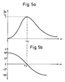
- Figs.5a and 5b are Bode plots of the magnitude and phase characteristics, respectively, for a resonant circuit about its resonant frequency;
- Fig. 6 is a block diagram of the preferred embodiment interrogator;
- Fig. 7 is a block diagram of the antenna circuit of the preferred embodiment interrogator;
- Fig. 8 is a schematic diagram of the preferred embodiment tuning circuit;
- Fig. 9 is a waveform graph for an antenna circuit having a resonant frequency less than that of the input signal received from the RF module;
- Fig. 10 is a waveform graph for an antenna circuit having a resonant frequency greater than that of the input signal received from the RF module;
- Fig. 11 is a waveform graph for an antenna circuit having a resonant frequency approximately equal to that of the input signal received from the RF module;
- Fig. 12 is a flow diagram for a prior art method of tuning the interrogator antenna;
- Fig. 13 is a flow diagram for a first method of tuning the interrogator antenna;
- Fig. 14 is a flow diagram for a second method of tuning the interrogator antenna;
- Fig. 15 is a flow diagram for a third method of tuning the interrogrator antenna; and
- Fig. 16 is a block diagram of a preferred embodiment demodulation circuit employing the phase correlation criterion.
- Corresponding numerals and symbols in the different figures refer to corresponding parts unless otherwise indicated.
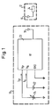
- Fig.1 shows a block diagram of an RFID system. In this system an
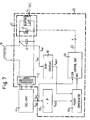
interrogator 10 is operable to send RF interrogations to a transponder 12. The transponder 12 has anantenna 16 and control circuitry 14. Theinterrogator 10 has anantenna 18 and anRF module 20. Theinterrogator 10 is preferably constructed to be held in the hand of an operator and to transmit an RF interrogation pulse. The transponder 12 is preferably a small, self-contained unit having no power source of its own.Interrogator 10 also can receive RF signals from the transponder 12 and detecting information contained in the RF signals. According to this embodiment transponder 12 replies to the transmission of an RF interrogation pulse by sending back the RF signal having the same frequency as the interrogation pulse. Preferably the RF signal is modulated with data by the transponder 12 using frequency shift keying (FSK) modulation. Operating power is supplied to theRF module 10 by alogic power supply 22 and atransmitter power supply 24. The current, ISL, fromlogic power supply 22 is supplied to the VSL input of theRF module 20. The transmitter operating current, ISP, is provided by thetransmitter power supply 24 to the input VSP input of theRF module 20. - Fig. 2 is a block diagram of a prior art interrogator tuning arrangement. In this prior art embodiment, an RF module 20a is provided which is in electrical communication with an
antenna 18. Theantenna 18 is coupled to osc/xmit circuitry 44 andreceiver circuitry 45 through atransformer 42. The osc/xmit circuitry 44 is powered at its VSP input that provides power for the oscillator to continue to oscillate and for a transmitter to drive theantenna 18. The voltage for the VSP input is provided bytransmitter power supply 24. The VSL inputs to osc/xmit circuitry 44 andreceiver circuitry 45 and provides power for the receive and transmit logic. Voltage for the VSL input is provided bylogic power supply 22.Antenna 18 andcapacitor 46 makeup the antennaresonant circuit tuning circuit 48 in the RF module 20a via connection 208. - Still referring to Fig.2, one prior art method of measuring the degree of tuning between the antenna
resonant circuit xmit circuitry 44 is to measure the power supply current into the supply voltage pin, VSP, for the osc/xmit circuitry 44 of theinterrogator 10. The supply current into this pin will be at a maximum when the resonant frequency, fres, of the antennaresonant circuit resonant circuit tuning circuit 48 not to monotonically increase in capacitance as the input frequency, fosz, is approached. Because of this difficulty, it is necessary to check at least one other measurement after the measured amplitudes have stopped increasing and began decreasing to ensure the true peak has been passed. The other difficulties with this method come with making connections from the ammeter 202 to the prior art RF module 20a. Further, a connection 208 from the microprocessor 200 to thetuning circuit 48 of the prior art RF module 20a must be made. Additionally, connections 210,212,214 must be made to connect the ammeter 202 and aswitch 206 in series with the ISP supply line. It is of course possible to embed all the extraneous tuning circuitry including the microprocessor 200 and the ammeter 202 in the RF module 20a to avoid having external connections. Embedding this circuitry, however, increases the difficulty of making changes to the tuning procedure by changing the microprocessor programming. Further, the cost, size, and power consumption of the prior art RF module 20a may be increased by embedding this circuitry therein. - Also shown in Fig.2 is an alternative embodiment for measuring the degree of tuning between the prior art RF module 20a and the antenna
resonant circuit antenna 18 to measure the field strength generated by the prior art RF module 20a driving theantenna 18. An RF voltage is induced in the pickup coil 204 by theantenna 18. The pickup coil 204 may then transmit the field strength information to the microprocessor 200 through the external connection 208, just as the ammeter 202 transmitted the current, ISP, information. This embodiment from this point has the same disadvantages of not having absolute measurements with which to determine a peak and of having false peaks as shown in Fig. 3. Further this embodiment also requires an external connection from the microprocessor 200 to the prior art RF module 20a. - Fig.4 is a block diagram of the preferred embodiment interrogator tuning arrangement. An
RF module 20b is provided which is in electrical communication with anantenna 18. Theantenna 18 is coupled to osc/xmit circuitry 44 andreceiver circuitry 45 through atransformer 42. The osc/xmit circuitry 44 is powered at its VSP input, which provides power for the oscillator to continue to oscillate and for a transmitter to drive theantenna 18. The voltage for the VSP input is provided bytransmitter power supply 24. The VSL inputs to osc/xmit 44 andreceiver 45 circuitry provide power for the receive and transmit logic. Voltage for the VSL input is provided bylogic power supply 22.Antenna 18 andcapacitor 46 makeup the antennaresonant circuit control circuit 220, which receives a reference signal "osz" from the osc/xmit stage 44. The control circuit compares the phase of the signal "osz" to the "res" signal. The preferred embodiment makes use of a characteristic of resonant circuits that is illustrated in Figs. 5a -5b. This characteristic is the transfer function of aresonant circuit resonant circuit resonant circuit resonant circuit tuning circuit 48 until the phase lead/lag is reduced to within a pre-defined tuning error. The phase difference between these two signals is now an absolute measurement, which can be used to great advantage in the present invention. The tuning method will be described in greater detail herein, but generally provides a less expensive, faster technique. - Fig. 6 is a block diagram of a
preferred embodiment interrogator 10. Theinterrogator 10 receives operating power at inputs VSP and VSL. TheRF module 20b has built-insupply voltage regulators logic 30 and the receivelogic 34. Theseregulators xmit stage 26 receives its supply voltage over lines VSP and GNDP. Inside theRF module 20b, the power ground line GNDP is decoupled from GND by theresistor 28. Thetransmitter control logic 30 generates a transmitter clock signal "osz" of frequency, fosz, from a crystal controlled oscillator (not shown). The transmitter clock signal is amplified by the osc/xmit stage 26 and is provided to theantenna circuit 32 of theRF module 20b. Thetransmitter logic 30 is active since the transmitter control line TXCT_is "low". - The
selective receiver 34 amplifies and demodulates the FSK signal received from theantenna 18. Thereceiver interface 36 converts the demodulated signal to LS-TTL and HCMOS-logic compatible data signals RXCK and RXDT, which contain the data, control and check bits. Conversion of the demodulated signal to logic levels occurs only after the TXCT_signal is active for a minimum time of TXmin. After the TXCT_signal has become inactive, the conversion occurs for a minimum time of TRXmin. The signal RXCK is a reference clock signal used to decode the RXDT data stream. The RXCK signal changes from "low" to "high" level in the middle of each data bit. - The signal RXSS_ switches to "low," if the received RF signal strength exceeds a predefined level, which can be adjusted with
potentiometer 38 in the RF module. - The
interrogator antenna 18 is preferably a coil, which is driven by the antenna circuit 32 (see also Fig. 7). As mentioned, for optimal operation of the transmit and receive function, theantenna resonance circuit - The
interrogator antenna 18 should have a high quality factor. In the preferred embodiment this antenna uses an RF litz-wire with a maximum single wire diameter of 0.1 mm. Preferably the litz wire will have at least 120 single insulated wires. - Fig. 7 is a block diagram showing the
antenna circuit 32 and the osc/xmit stage 26 in greater detail. The osc/xmit stage has osc/xmit circuitry 44 that is connected toantenna resonance circuit transformer 42. With acapacitor 46,coil 18 forms anantenna resonance circuit Tuning circuit 48 is provided in parallel tocapacitor 46 so that the resonance frequency of the antennaresonant circuit control circuit 50 is provided to control thetuning circuit 48 over a tuningbus 52.Tuning bus 52 has a predetermined number of connections depending on the number of tuning capacitors within thetuning circuit 48. A dampingcircuit 54 is provided to enable fast reception from the transponder 12 after TXCT_has been low (active). The osc/xmit circuitry 44 provides a first signal to the input oftransformer 42 that in turn provides a second signal as its output toantenna resonance circuit xmit circuitry 44 to aphase shifter 56 and acontrol unit 50. The signal "osz" is a reference signal that has the same phase and frequency as the first signal provided to thetransformer 42. The antennaresonant circuit xmit stage 44 by providing the output of thetransformer 42 as a second signal in response to the first signal. In the antenna circuitry 32 atuning circuit 48 is provided in parallel with thecapacitor 46, thetuning circuit 48 being selectable to variably modify the resonance frequency of theresonant circuit coil 18 and thecapacitor 46. At the antennaresonant circuit 18,46 a phase correlation signal, "res," is provided, the form of "res" being substantially a sine wave having an apex that lags the falling edge of the first signal when the resonance frequency, fres, of theantenna circuit antenna circuit antenna circuit - In the preferred embodiment of the invention, the magnitude of the phase difference between the apex of the sine wave and the falling edge of the first signal is called the phase difference. The phase difference monotonically decreases as the resonant frequency, fres, of the antenna tuned
circuit crossing detector 56 receives the correlation signal, "res," and conditions this signal to be substantially a square wave for compatibility with digital logic circuitry. Still further included in the exemplary embodiment is aphase shifter 58 that induces a phase shift in the first signal to correspond to the phase shift that is inherently induced in the zerocrossing detector 56. - A
comparator 60 then receives the outputs of the zerocrossing detector 56 and thephase detector 58.Comparator 60 then provides an output of a first logic level when the output of the zerocrossing detector 56 is of lesser amplitude than the output of thephase shifter 58 or of a second logic level when the output of the zerocrossing detector 56 is of greater amplitude than the output of thephase shifter 58. Acontrol circuit 50 is provided for adjusting the resonant frequency, fres, of theresonant circuit tuning circuit 48 in response to the signals received from thecomparator 60. The details of how thecomparator 60 andtuning circuit 58 respond to the signals received fromphase shifter 58 and from zerocrossing detector 56 to effect automatic tuning of the antennaresonant circuit - Fig. 8 is a schematic diagram of the
tuning circuit 48. It receives inputs ATC1, ATC2, ATC3, ATC4 ATC5, ATC6 and ATCX from tuningbus 52. The input ATC1 closes the switch 67 that connects acapacitor 66 having a weighted value of "one" in parallel withcapacitor 46. The input ATC2 closes the switch 69 that connects acapacitor 68 having a weighted value of "two" in parallel with thecapacitor 46. The input ATC3 closes the switch 71 that connects a capacitor 70 having a weighted value of "four" in parallel with thecapacitor 46. Inputs ATC4, ATC5 and ATC6 act in a similar manner forcapacitors capacitor 64 is provided in series with the switch 65 controlled by input ATCX. The procedures for controlling these switches will be described in greater detail during discussion of Figs. 13-15. - Fig. 9 is a waveform graph for an antenna circuit having a resonant frequency, fres, less than the frequency, fosz, of the reference signal received from the RF module.
Signal 1 of Fig. 9 shows the reference signal from the RF module transmitter. Markings showing a half oscillation period (T/2) and a quarter oscillation period (T/4) are shown.Signal 2 of Fig. 9 shows the voltage at theantenna circuit Signal 3 is generated fromSignal 2 by the zero-crossing circuit 56.Signal 4 is generated by thephase shifter 58 fromSignal 1. The zero-crossing circuit 56 receivesSignal 2 and converts the signal into a digital format for compatible operation with the logic circuitry. Arrows "A" and "B" show the correspondence between the zero crossings ofSignal 2 and the transitions ofSignal 3. Arrow "C" shows the raw resonance criteria between Vosz and Vat. As can be seen by Arrow "C," the falling edge of the oscillator reference signal,Signal 1, leads the peak of the voltage at theantenna circuit Signal 2 as shown inSignal 3 by a zerocrossing detector 56. It is further desirable to facilitate these comparisons by phase shifting the reference signal,Signal 1, by phase shifting it to formSignal 4 as shown by Arrow "D". In this way a usable resonance criteria is formed in which the phase of the output of the zerocrossing detector 56,Signal 3, is compared to that of the output of thephase shifter 58,Signal 4. For the raw resonance criteria, the transition ofSignal 1 corresponds at the tuned frequency when to the peak ofSignal 2. In the tuned condition for the usable resonance criteria, however, thesignals Signal 3 andSignal 4 will both have simultaneous transitions. In Fig. 9, Arrow "E" shows that the falling edge ofSignal 4 leads the rising edge ofSignal 3, indicating that the resonant frequency of theantenna circuit Signals - Fig. 10 is a waveform graph for an
antenna circuit Signal 4 lags the rising edge ofSignal 3, indicating that the resonant frequency of theantenna circuit - Fig. 11 shows the waveform graph for an antenna circuit having a resonant frequency approximately equal to that of the signal received from the RF module. As earlier stated, in this condition the falling edge of
Signal 4 will occur simultaneously with the rising edge ofSignal 3. Although the magnitude of the signal at theantenna circuit - Fig.12 is a flow chart illustrating the procedure for tuning an antenna circuit in the prior art. From the
start block 80, the procedure begins atblock 82 where the antenna circuit is enabled by the signal TXCT_. Since this signal is a "low" active signal then the antenna is enabled by taking the signal "low." Once the antenna is enabled, the relative degree of tuning can be measured using known prior art techniques, such as measuring the field strength in proximity to theantenna 18 or measuring the current into the osc/xmit stage 26. The next step occurs atblock 84 at which the frequency is set to a minimum, fmin by closing all the switches, 65,67,69,71,73,75,77 of the tuning/dampingcircuit 62. This gives the tuning procedure a known starting point from which a consistent method can be used. The next step is atblock 86 in which the field strength is measured by the field strength detector 202 in close proximity to theantenna 18 or at which the current into the osc/xmit stage 26 is measured by ammeter 204 in series with the VSP supply voltage. As mentioned, the difficulty with the prior art tuning method comes from having always to compare the strength of the oscillation in theantenna resonance circuit block 86, a second reading must be taken at a new frequency, thus atblock 88 the tuning capacity of thetuning circuit 48 is increased by one step. The weighting increments might be in binary steps for a set of binarily-weighted capacitors. Depending on the method, however, another step size might be used. Now atblock 90 the field strength is measured again. Atdecision block 92 the new field strength is compared to the old field strength. If this new field strength is greater than the old field strength, then the method returns to block 88 and blocks 88 and 90 are repeated. A new decision is then made at 92 using the newest field strength measurement atblock 90 and the previously-measured field strength fromblock 90. If, however, atblock 92 the new field strength is less than the old field strength, the procedure moves to block 94 where the tuning capacitance is increased by another tuning step. The field strength is then measured again atblock 96 and again anew decision block 98 is encountered. This new field strength is compared to the prior field strength this time as measured inblock 90. If this field strength is greater than the old field strength, the execution again returns to block 88 to repeat this procedure. If the new field strength is less than the old field strength, the method goes on fromblock 100 where the tuning capacitance is decreased by two steps to compensate for the two step increases in tuning capacity atblocks 88 andblock 94. Thestep 100 is necessary because in this method it is not known when the correct tuned frequency has been exceeded until the measured field strengths or current begins to decrease from its peak. Thus, the two steps in which the field strength decreased while the tuning circuit determined that the optimal resonant frequency had been exceeded must be undone. The reason that blocks 88,90,92 are essentially repeated asblocks resonant circuit - Fig.13 illustrates the improved tuning procedure using the phase correlation criterion. This procedure continues from the
start block 110 and block 112 in which the antenna is enabled by a low assertion of TXCT_. The procedure continues atblock 114 at which all switches are closed to set the frequency of the tuned circuit to its minimum, fmin. At block 116 a phase difference is calculated between a signal measured directly at the antenna resonance circuit, "res," and a reference signal, "osz," received directly from the osc/xmit stage 26. At decision block 118 a simple criterion is used to determine if the tuning procedure should continue. It the phase difference between "res" and "osc" is greater than zero, the tuning procedure continues. If atdecision block 118 the frequency difference is greater than zero, the procedure continues to block 120 where the tuning capacitance of the tuning circuit is increased by one binary step. The frequency difference is measured again at block 116 and the decision atblock 118 is repeated until the phase difference changes signs from positive to negative. As the frequency is increased in steps from fmin by the tuning circuit, the phase difference will gradually decrease in magnitude until it changes sign when fres becomes greater than fosz. Of course the procedure ends atstop block 122. - Fig.14 shows an alternative inventive method for tuning an antenna circuit. This procedure is the same as that described in Fig. 13, except for two steps that are inserted. Step 115 is inserted between
step 114 and 116. Step 115 consists of connection of theauxiliary capacitor 64 in parallel with thecapacitor 46.Auxiliary capacitor 64 is connected tocapacitor 64 by switch 65 that is controlled by input ATCX.Auxiliary capacitor 64 has a magnitude of half that of the capacitance of the smallest tuning capacitor. The normal tuning procedure is initiated at this point until again the frequency difference changes signs from positive to negative atdecision block 118. At this time theauxiliary capacitor 64 is disconnected atblock 121. The difference between this procedure and the procedure of Fig. 14 is like the difference between truncation and rounding. The prior method of Fig. 13 is like truncation in that the procedure continues until the target frequency is exceeded, thus the frequency error between the antenna resonant circuit can be up to +1 step and of course will never be less. In the method of Fig. 14, theauxiliary capacitor 64 has half the value of the minimum tuning capacitor. Theauxiliary capacitor 64 is disconnected after the tuning procedure has been completed, thus the most frequency fres of the antennaresonant circuit resonant circuit - With the described tuning methods, tuning is possible even during the powering burst because the magnitude of the oscillation within the
antenna resonance circuit antenna resonance circuit antenna resonance circuit step 120 or 120a is then executed, before the dynamic tuning circuit returns to step 116. The "Dynamic Auto Tuning" method is very useful in instances where theantenna 18 is subject to detuning at any time such as from a metal object in close proximity to theantenna 18. - The three procedures detailed in Fig.13-15 are but examples of procedures that can be used advantageously with the phase correlation criterion. Many other methods are foreseen by the applicant. For example, successive approximation adjustments could be used to more quickly tune the resonant circuit. Successive approximation can not be used in the prior art circuit because an absolute criterion must be used to determine if and how much the capacity of the resonant circuit must be increased or decreased. As mentioned, the tuning steps might be binary steps or they might be logarithmic or other weightings could be used.
- Since the described tuning methods are so much faster than prior known methods, tuning can be accomplished with each transmit burst if desired. The simplicity of this method allows the tuning to be accomplished with a hardware implementation. The prior art methods require more sophisticated, more complex circuitry in which a new strength measurement must be compared to an old measurement. Thus, memory must be used with the prior art methods. Furthermore, the phase correlation criterion is less dependent on temperature than the magnitude of the oscillation within the
antenna resonance circuit resonant circuit - Fig. 16 applies the same principles used hereinabove for use as an
FSK data demodulator 300. A resonant circuit is formed from the parallel combination ofcoil 302 andcapacitor 304. In this embodiment, the resonant frequency, fres, of resonant circuit 302,304 is selected to be between the two modulated FSK frequencies, f₁ and f₂. Thebuffers 308 provide isolation in the normal fashion. As described hereinabove, when the input frequency is f₁, where f₁ is less than fres, the output of the comparator or flip-flop 306 has a first value. When the input frequency is f₂, where f₂ is greater than fres, the output of thecomparator 306 will have another value. - The sole table, below, provides an overview of the embodiments and the drawings:


- A few preferred embodiments have been described in detail hereinabove. It is to be understood that the scope of the invention also comprehends embodiments different from those described, yet within the scope of the claims.
- For example, "microcomputer" in some contexts is used to mean that microcomputer requires a memory and "microprocessor" does not. The usage herein is that these terms can also be synonymous and refer to equivalent things. The phrase "processing circuitry" or "control circuitry" comprehends ASICs (application specific integrated circuits), PAL (programmable array logic), PLAs (programmable logic arrays), decoders, memories, non-software based processors, or other circuitry, or digital computers including microprocessors and microcomputers of any architecture, or combinations thereof. Memory devices include SRAM (static random access memory), DRAM (dynamic random access memory), pseudo-static RAM, latches, EEPROM (electrically-erasable programmable read-only memory), EPROM (erasable programmable read-only memory), registers, or any other memory device known in the art. Words of inclusion are to be interpreted as nonexhaustive in considering the scope of the invention.
- Implementation is contemplated in discrete components or fully integrated circuits in silicon, gallium arsenide, or other electronic materials families, as well as in optical-based or other technology-based forms and embodiments. It should be understood that various embodiments of the invention can employ or be embodied in hardware, software or microcoded firmware.
- While this invention has been described with reference to illustrative embodiments, this description is not intended to be construed in a limiting sense. Various modifications and combinations of the illustrative embodiments, as well as other embodiments of the invention, will be apparent to persons skilled in the art upon reference to the description. It is therefore intended that the appended claims encompass any such modifications or embodiments.
Claims (19)
- A method of matching the resonant frequency of an antenna resonant circuit to the output frequency of a transmitter output stage, the method comprising the steps of:a) providing a powering signal from said transmitter output stage to said antenna resonant circuit;b) receiving at said antenna resonant circuit said powering signal, said antenna resonant circuit comprising a tuning circuit, said tuning circuit being operable to variably modify said resonant frequency of said resonant circuit, said antenna resonant circuit having at its output a phase correlation signal, the phase of said phase correlation signal relative to said powering signal having a known relationship to the frequency difference between said resonant frequency and said powering signal;c) receiving in a phase comparator said powering signal and said phase correlation signal; andd) adjusting the resonant frequency of said resonant circuit in response to the received output of said phase comparator.
- The method of claim 1 wherein said resonant circuit further comprises a coil and a capacitor.
- The method of claim 2 wherein said tuning circuit is a network of capacitors in parallel with said coil and said capacitor.
- The method of claim 3 wherein the parallel resonant frequency of said coil and said capacitor is chosen to be less than a known minimum frequency of said powering signal and wherein the resonant frequency of said resonant circuit is adjusted by decreasing the capacity of the tuning circuit in steps until the resonant frequency of said resonant circuit is increased from its initial value to be approximately equal to the frequency of said powering signal.
- The method of claim 3 wherein said network of capacitors is a set of binary-weighted tuning capacitors to be connected in parallel to said resonant circuit.
- The method of claim 5 wherein said set of binary-weighted tuning capacitors is done by binary tuning steps such that the capacity of said tuning circuit is increased in approximately linear fashion.
- The method of claim 5 wherein said set of binary-weighted tuning capacitors is done by successive approximation.
- The method of claim 3 wherein said network of capacitors is a set of logarithmically-weighted tuning capacitors to be connected in parallel to said resonant circuit.
- The method of claim 8 wherein said step enabling or disabling of said set of logarithmically-weighted tuning capacitors is done by adaptive methods whereby the size of the tuning step is proportional to the magnitude of the phase difference between said powering signal and said phase correlation signal.
- A method of matching the resonant frequency of an antenna resonant circuit to the output frequency of a transmitter output stage, the method comprising the steps of:a) providing a powering signal from said transmitter power stage to a powering winding of a transformer, the form of said powering signal being substantially a square wave having rising and falling edges, the frequency of said powering signal not precisely known but known to fall between a minimum and a maximum frequency;b) providing by said transformer at a second winding thereof, an antenna signal in response to said powering signal;c) receiving at said antenna resonant circuit said antenna signal, said antenna resonant circuit comprising a coil, a capacitor, and a tuning circuit, said coil and said capacitor being serially connected between the first and second terminals of said second winding and defining a resonant circuit output at the connection between said coil and said capacitor, and said tuning circuit being in parallel with said capacitor and being operable to variably modify the resonance frequency of said resonant circuit from the initial resonance frequency of the parallel combination of said coil and said capacitor;d) providing at said output of said antenna resonant circuit a phase correlation signal, the form of which is substantially a sine wave having an apex which:i) lags the falling edge of said powering signal when the resonance frequency of said antenna circuit is less than the frequency of said powering signal;ii) is approximately at the falling edge of said powering signal when the resonance frequency of said antenna circuit is approximately at the frequency of said powering signal; andiii) leads the falling edge of said powering signal when the resonance frequency of said antenna circuit is greater than the frequency of said powering signal,
the magnitude of the distance between the apex of said sine wave and the falling edge of said powering signal being the phase difference, said phase difference being related to the magnitude of the frequency difference between said resonance frequency and said powering signal;e) receiving by a zero crossing detector said correlation signal and conditioning this signal to be substantially a square wave for compatibility with digital logic circuitry;f) receiving by a phase shifter said powering signal, said phase shifter including a phase shift in said powering signal to correspond to the phase shift which is inherently induced in said zero crossing detector;g) receiving in a phase comparator the outputs of said zero crossing detector and said phase detector, said phase comparator providing an output of a first logic level when the phase difference is less than a reference value and of a second logic level when the phase difference is greater than a reference value; andh) adjusting the resonant frequency of said resonant circuit by a control unit in response to the received output from said phase comparator. - A circuit arrangement for matching the resonant frequency of an antenna resonant circuit to the output frequency of a transmitter output stage comprising:a) a transmitter output stage providing a powering signal;b) an antenna resonant circuit for receiving said powering signal, said antenna resonant circuit having a predetermined resonant frequency and comprising a tuning circuit wherein said resonant frequency is dependent upon the value of said tuning circuit, said antenna resonant circuit having at its output a phase correlation signal, the phase of said phase correlation signal relative to said powering signal having a known relationship to the frequency difference between said resonant frequency and said powering signal; andc) a phase comparator for receiving said powering signal and said phase correlation signal and measuring the phase difference therebetween, said phase comparator further for controlling said tuning circuit to adjust the resonant frequency of said resonant circuit depending upon said phase difference.
- The circuit arrangement of claim 11 wherein said resonant circuit further comprises a coil and a capacitor.
- The circuit arrangement of claim 12 wherein said tuning circuit is a network of capacitors in parallel with said coil and said capacitor.
- The circuit arrangement of claim 13 wherein the parallel resonant frequency of said coil said capacitor is chosen to be less than a known minimum frequency of said powering signal and wherein the resonant frequency of said resonant circuit is adjusted by decreasing the capacity of the tuning circuit in steps until the resonant frequency of said resonant circuit is increased from its initial value to be approximately equal to the frequency of said powering signal.
- The circuit arrangement of claim 13 wherein said network of capacitors is a set of binary-weighted tuning capacitors to be connected in parallel to said resonant circuit.
- The circuit arrangement of claim 15 wherein said set of binary-weighted tuning capacitors is done by binary tuning steps such that the capacity of said tuning circuit is increased in approximately linear fashion.
- The circuit arrangement of claim 15 wherein said set of binary-weighted tuning capacitors is done by successive approximation.
The circuit arrangement of claim 13 wherein said network of capacitors is a set of logarithmically-weighted tuning capacitors to be connected in parallel to said resonant circuit. - The circuit arrangement of claim 18 wherein said step enabling or disabling of said set of logarithmically-weighted tuning capacitors is done by adaptive circuit arrangements whereby the size of the tuning step is proportional to the magnitude of the phase difference between said powering signal and said phase correlation signal.
- A method of FSK demodulation, matching the resonant frequency of an antenna resonant circuit to the output frequency of a transmitter output stage, the method comprising the steps of:a) receiving an FSK-modulated data transmission having a first and a second FSK frequency;b) providing an antenna resonant circuit, said antenna resonant circuit having a resonant frequency between said first and said second FSK frequencies;c) receiving at said antenna resonant circuit FSK-modulated data transmission;d) providing from said antenna resonant circuit a phase correlation signal, the phase of said phase correlation signal relative to said FSK-modulated data transmission having a known relationship to the frequency difference between said resonant frequency and said FSK-modulated data transmission;e) receiving in a phase comparator said FSK-modulated data transmission and said phase correlation signal; andf) providing a demodulated data stream from said phase comparator in response to receiving said FSK-modulated data transmission and said phase correlation signal and operating to differentiate between a condition when the frequency of the FSK-modulated data transmission is less than the resonant frequency and a condition when the frequency of the FSK-modulated data transmission is less greater the resonant frequency based on the known relationship of the phase difference therebetween and the frequency difference between the FSK modulated data transmission and the resonant frequency of the resonant circuit.
Applications Claiming Priority (2)
| Application Number | Priority Date | Filing Date | Title |
|---|---|---|---|
| US08/083,810 US5491715A (en) | 1993-06-28 | 1993-06-28 | Automatic antenna tuning method and circuit |
| US83810 | 1993-06-28 |
Publications (3)
| Publication Number | Publication Date |
|---|---|
| EP0663724A2 true EP0663724A2 (en) | 1995-07-19 |
| EP0663724A3 EP0663724A3 (en) | 1995-11-22 |
| EP0663724B1 EP0663724B1 (en) | 2000-09-27 |
Family
ID=22180855
Family Applications (1)
| Application Number | Title | Priority Date | Filing Date |
|---|---|---|---|
| EP94109995A Expired - Lifetime EP0663724B1 (en) | 1993-06-28 | 1994-06-28 | Method of automatic antenna tuning and of demodulation of a FSK modulated signal, respectively |
Country Status (4)
| Country | Link |
|---|---|
| US (1) | US5491715A (en) |
| EP (1) | EP0663724B1 (en) |
| JP (1) | JPH07193516A (en) |
| DE (1) | DE69426013T2 (en) |
Cited By (14)
| Publication number | Priority date | Publication date | Assignee | Title |
|---|---|---|---|---|
| FR2743962A1 (en) * | 1996-01-23 | 1997-07-25 | Siemens Ag | DATA OR ENERGY TRANSMISSION DEVICE, IN PARTICULAR FOR ANTI-THEFT SYSTEM FOR A MOTOR VEHICLE |
| EP1047191A1 (en) * | 1999-04-19 | 2000-10-25 | Nokia Mobile Phones Ltd. | Method and arrangement for tuning a resonator |
| FR2847089A1 (en) * | 2002-11-12 | 2004-05-14 | Inside Technologies | Antenna circuit for non-contact integrated circuit drive, has filter with point for detecting electrical voltage, whose amplitude forms relevant information to tune circuit to determined resonance frequency |
| FR2894047A1 (en) * | 2005-11-25 | 2007-06-01 | Spacecode | Inductor for e.g. support, has conductors distributed over surface and connected with each other by connection conductors for forming circuit strands whose ends are connected to power supply circulating electric current in conductors |
| WO2007115911A2 (en) * | 2006-04-05 | 2007-10-18 | Continental Automotive Gmbh | Method for operating a vibrating gyroscope and sensor arrangement |
| EP2086122A2 (en) * | 2008-02-01 | 2009-08-05 | Korea Advanced Institute of Science and Technology | Apparatus and method for compensating for inductance in inductive coupling communications |
| WO2010055321A1 (en) * | 2008-11-14 | 2010-05-20 | Cambridge Resonant Technologies Limited | Tuned resonant circuits |
| EP2195880A1 (en) * | 2007-09-24 | 2010-06-16 | Cooper Tire & Rubber Company | Automatic antenna tuner system for rfid |
| US8085133B2 (en) | 2007-05-18 | 2011-12-27 | Cambridge Resonant Technologies Ltd. | RFID interrogator |
| WO2013075758A1 (en) * | 2011-11-25 | 2013-05-30 | Widex A/S | Automatic fsk tuning circuit for a hearing aid and method |
| EP2634928A4 (en) * | 2010-10-29 | 2015-04-29 | Sony Corp | Portable communication device, reader/writer device, and resonant frequency adjustment method |
| WO2016062992A1 (en) * | 2014-10-24 | 2016-04-28 | William Redman-White | Electronic tuning system |
| US9706315B2 (en) | 2013-02-07 | 2017-07-11 | Widex A/S | Transceiver for a hearing aid and a method for operating such a transceiver |
| US10154649B2 (en) | 2005-12-16 | 2018-12-18 | Cambridge Resonant Technologies Ltd. | RFID reader |
Families Citing this family (197)
| Publication number | Priority date | Publication date | Assignee | Title |
|---|---|---|---|---|
| US6219015B1 (en) | 1992-04-28 | 2001-04-17 | The Board Of Directors Of The Leland Stanford, Junior University | Method and apparatus for using an array of grating light valves to produce multicolor optical images |
| DE4327642C2 (en) * | 1993-05-17 | 1998-09-24 | Anatoli Stobbe | Reader for a detection plate |
| US6472975B1 (en) * | 1994-06-20 | 2002-10-29 | Avid Marketing, Inc. | Electronic identification system with improved sensitivity |
| US6219529B1 (en) * | 1994-07-19 | 2001-04-17 | Seiko Instruments Inc. | Wireless communication system using only the magnetic field component |
| US5841579A (en) | 1995-06-07 | 1998-11-24 | Silicon Light Machines | Flat diffraction grating light valve |
| NL1001840C2 (en) * | 1995-12-07 | 1997-06-10 | Nederland Ptt | Label. |
| US6650870B2 (en) * | 1995-12-15 | 2003-11-18 | Innovision Research & Technology Plc | Data communication apparatus |
| SG46175A1 (en) * | 1996-01-10 | 1998-02-20 | Philips Electronics Nv | Tv/fm receiver for multi-media applications |
| SE507698C2 (en) * | 1996-07-10 | 1998-07-06 | Allgon Ab | Method and system for tuning resonance modules |
| US6466131B1 (en) * | 1996-07-30 | 2002-10-15 | Micron Technology, Inc. | Radio frequency data communications device with adjustable receiver sensitivity and method |
| WO1998011496A1 (en) * | 1996-09-13 | 1998-03-19 | Temic Telefunken Microelectronic Gmbh | Data transfer method for a scanning identification system |
| EP0871897A1 (en) * | 1996-11-05 | 1998-10-21 | Koninklijke Philips Electronics N.V. | Contactless data transmission and receiving device with a synchronous demodulator |
| US5991609A (en) * | 1996-12-26 | 1999-11-23 | Delco Electronics Corporation | Low cost digital automatic alignment method and apparatus |
| TW376598B (en) * | 1997-02-05 | 1999-12-11 | Em Microelectronic Marin Sa | Base station for a contactless interrogation system comprising a phase locked and voltage controlled oscillator |
| US5982553A (en) | 1997-03-20 | 1999-11-09 | Silicon Light Machines | Display device incorporating one-dimensional grating light-valve array |
| US6057779A (en) | 1997-08-14 | 2000-05-02 | Micron Technology, Inc. | Method of controlling access to a movable container and to a compartment of a vehicle, and a secure cargo transportation system |
| US6088102A (en) | 1997-10-31 | 2000-07-11 | Silicon Light Machines | Display apparatus including grating light-valve array and interferometric optical system |
| US6356535B1 (en) * | 1998-02-04 | 2002-03-12 | Micron Technology, Inc. | Communication systems and methods of communicating |
| US6271808B1 (en) | 1998-06-05 | 2001-08-07 | Silicon Light Machines | Stereo head mounted display using a single display device |
| US6130770A (en) | 1998-06-23 | 2000-10-10 | Silicon Light Machines | Electron gun activated grating light valve |
| US6101036A (en) | 1998-06-23 | 2000-08-08 | Silicon Light Machines | Embossed diffraction grating alone and in combination with changeable image display |
| US6215579B1 (en) | 1998-06-24 | 2001-04-10 | Silicon Light Machines | Method and apparatus for modulating an incident light beam for forming a two-dimensional image |
| FR2781587B1 (en) * | 1998-07-21 | 2000-09-08 | Dassault Electronique | ADVANCED READER FOR NON-CONTACT BADGES |
| US6303986B1 (en) | 1998-07-29 | 2001-10-16 | Silicon Light Machines | Method of and apparatus for sealing an hermetic lid to a semiconductor die |
| US6317027B1 (en) | 1999-01-12 | 2001-11-13 | Randy Watkins | Auto-tunning scanning proximity reader |
| US8538801B2 (en) | 1999-02-19 | 2013-09-17 | Exxonmobile Research & Engineering Company | System and method for processing financial transactions |
| US8636648B2 (en) | 1999-03-01 | 2014-01-28 | West View Research, Llc | Endoscopic smart probe |
| US10973397B2 (en) | 1999-03-01 | 2021-04-13 | West View Research, Llc | Computerized information collection and processing apparatus |
| US6400272B1 (en) | 1999-04-01 | 2002-06-04 | Presto Technologies, Inc. | Wireless transceiver for communicating with tags |
| US8065155B1 (en) | 1999-06-10 | 2011-11-22 | Gazdzinski Robert F | Adaptive advertising apparatus and methods |
| US6714121B1 (en) | 1999-08-09 | 2004-03-30 | Micron Technology, Inc. | RFID material tracking method and apparatus |
| US7710273B2 (en) * | 1999-09-02 | 2010-05-04 | Round Rock Research, Llc | Remote communication devices, radio frequency identification devices, wireless communication systems, wireless communication methods, radio frequency identification device communication methods, and methods of forming a remote communication device |
| US7070112B2 (en) * | 1999-09-07 | 2006-07-04 | American Express Travel Related Services Company, Inc. | Transparent transaction device |
| US7239226B2 (en) | 2001-07-10 | 2007-07-03 | American Express Travel Related Services Company, Inc. | System and method for payment using radio frequency identification in contact and contactless transactions |
| US7889052B2 (en) | 2001-07-10 | 2011-02-15 | Xatra Fund Mx, Llc | Authorizing payment subsequent to RF transactions |
| US7837116B2 (en) | 1999-09-07 | 2010-11-23 | American Express Travel Related Services Company, Inc. | Transaction card |
| US7093767B2 (en) * | 1999-09-07 | 2006-08-22 | American Express Travel Related Services Company, Inc. | System and method for manufacturing a punch-out RFID transaction device |
| US6693511B1 (en) | 1999-09-24 | 2004-02-17 | Ge Interlogix, Inc. | System and method for communicating with dormant radio frequency identification tags |
| US6452504B1 (en) | 1999-09-24 | 2002-09-17 | Ge Interlogix, Inc. | System and method for communication with radio frequency identification tags using tow message DFM protocol |
| US6661335B1 (en) | 1999-09-24 | 2003-12-09 | Ge Interlogix, Inc. | System and method for locating radio frequency identification tags |
| US6396438B1 (en) | 1999-09-24 | 2002-05-28 | Slc Technologies | System and method for locating radio frequency identification tags using three-phase antenna |
| US7268668B2 (en) * | 2003-05-09 | 2007-09-11 | American Express Travel Related Services Company, Inc. | Systems and methods for managing multiple accounts on a RF transaction instrument |
| US8543423B2 (en) | 2002-07-16 | 2013-09-24 | American Express Travel Related Services Company, Inc. | Method and apparatus for enrolling with multiple transaction environments |
| US8429041B2 (en) * | 2003-05-09 | 2013-04-23 | American Express Travel Related Services Company, Inc. | Systems and methods for managing account information lifecycles |
| US7172112B2 (en) | 2000-01-21 | 2007-02-06 | American Express Travel Related Services Company, Inc. | Public/private dual card system and method |
| AU2001243473A1 (en) | 2000-03-07 | 2001-09-17 | American Express Travel Related Services Company, Inc. | System for facilitating a transaction |
| DE60024225T2 (en) * | 2000-03-18 | 2006-08-03 | Siemens Ag | radio transmitter |
| US6806812B1 (en) | 2000-04-26 | 2004-10-19 | Micron Technology, Inc. | Automated antenna trim for transmitting and receiving semiconductor devices |
| FR2812142A1 (en) * | 2000-07-21 | 2002-01-25 | Microcid Sa | Contactless radio frequency transponder/identifier having transponder and reader with antennas with transponder having analogue circuit rectifier and clock extractor output variable level |
| EP1328888A4 (en) * | 2000-10-20 | 2004-10-27 | Promega Corp | Radio frequency identification method and system of distributing products |
| US20020183882A1 (en) | 2000-10-20 | 2002-12-05 | Michael Dearing | RF point of sale and delivery method and system using communication with remote computer and having features to read a large number of RF tags |
| USRE47599E1 (en) | 2000-10-20 | 2019-09-10 | Promega Corporation | RF point of sale and delivery method and system using communication with remote computer and having features to read a large number of RF tags |
| WO2002050758A1 (en) * | 2000-12-20 | 2002-06-27 | Fraunhofer-Gesellschaft zur Förderung der angewandten Forschung e. V. | Device and method for the simultaneous reading of passive inductive transponders |
| US6707591B2 (en) | 2001-04-10 | 2004-03-16 | Silicon Light Machines | Angled illumination for a single order light modulator based projection system |
| US7650314B1 (en) | 2001-05-25 | 2010-01-19 | American Express Travel Related Services Company, Inc. | System and method for securing a recurrent billing transaction |
| US7542942B2 (en) | 2001-07-10 | 2009-06-02 | American Express Travel Related Services Company, Inc. | System and method for securing sensitive information during completion of a transaction |
| US7725427B2 (en) * | 2001-05-25 | 2010-05-25 | Fred Bishop | Recurrent billing maintenance with radio frequency payment devices |
| US6747781B2 (en) | 2001-06-25 | 2004-06-08 | Silicon Light Machines, Inc. | Method, apparatus, and diffuser for reducing laser speckle |
| US6782205B2 (en) | 2001-06-25 | 2004-08-24 | Silicon Light Machines | Method and apparatus for dynamic equalization in wavelength division multiplexing |
| US8284025B2 (en) * | 2001-07-10 | 2012-10-09 | Xatra Fund Mx, Llc | Method and system for auditory recognition biometrics on a FOB |
| US7925535B2 (en) * | 2001-07-10 | 2011-04-12 | American Express Travel Related Services Company, Inc. | System and method for securing RF transactions using a radio frequency identification device including a random number generator |
| US8960535B2 (en) | 2001-07-10 | 2015-02-24 | Iii Holdings 1, Llc | Method and system for resource management and evaluation |
| US8001054B1 (en) | 2001-07-10 | 2011-08-16 | American Express Travel Related Services Company, Inc. | System and method for generating an unpredictable number using a seeded algorithm |
| US7705732B2 (en) | 2001-07-10 | 2010-04-27 | Fred Bishop | Authenticating an RF transaction using a transaction counter |
| US7762457B2 (en) * | 2001-07-10 | 2010-07-27 | American Express Travel Related Services Company, Inc. | System and method for dynamic fob synchronization and personalization |
| US8635131B1 (en) | 2001-07-10 | 2014-01-21 | American Express Travel Related Services Company, Inc. | System and method for managing a transaction protocol |
| US20040233038A1 (en) * | 2001-07-10 | 2004-11-25 | American Express Travel Related Services Company, Inc. | Method and system for retinal scan recognition biometrics on a fob |
| US7119659B2 (en) * | 2001-07-10 | 2006-10-10 | American Express Travel Related Services Company, Inc. | Systems and methods for providing a RF transaction device for use in a private label transaction |
| US20040232224A1 (en) * | 2001-07-10 | 2004-11-25 | American Express Travel Related Services Company, Inc. | Method for registering biometric for use with a fob |
| US7827106B2 (en) * | 2001-07-10 | 2010-11-02 | American Express Travel Related Services Company, Inc. | System and method for manufacturing a punch-out RFID transaction device |
| US7360689B2 (en) | 2001-07-10 | 2008-04-22 | American Express Travel Related Services Company, Inc. | Method and system for proffering multiple biometrics for use with a FOB |
| US20040257197A1 (en) * | 2001-07-10 | 2004-12-23 | American Express Travel Related Services Company, Inc. | Method for biometric security using a transponder-reader |
| US20040236700A1 (en) * | 2001-07-10 | 2004-11-25 | American Express Travel Related Services Company, Inc. | Method and system for keystroke scan recognition biometrics on a fob |
| US20040233037A1 (en) * | 2001-07-10 | 2004-11-25 | American Express Travel Related Services Company, Inc. | Method and system for iris scan recognition biometrics on a fob |
| US9031880B2 (en) | 2001-07-10 | 2015-05-12 | Iii Holdings 1, Llc | Systems and methods for non-traditional payment using biometric data |
| US7746215B1 (en) | 2001-07-10 | 2010-06-29 | Fred Bishop | RF transactions using a wireless reader grid |
| US7312707B1 (en) | 2001-07-10 | 2007-12-25 | American Express Travel Related Services Company, Inc. | System and method for authenticating a RF transaction using a transaction account routing number |
| US7429927B2 (en) | 2001-07-10 | 2008-09-30 | American Express Travel Related Services Company, Inc. | System and method for providing and RFID transaction device |
| US20040238621A1 (en) * | 2001-07-10 | 2004-12-02 | American Express Travel Related Services Company, Inc. | Method and system for fingerprint biometrics on a fob |
| US7463133B2 (en) * | 2001-07-10 | 2008-12-09 | American Express Travel Related Services Company, Inc. | Systems and methods for providing a RF transaction device operable to store multiple distinct calling card accounts |
| US7668750B2 (en) | 2001-07-10 | 2010-02-23 | David S Bonalle | Securing RF transactions using a transactions counter |
| US7805378B2 (en) * | 2001-07-10 | 2010-09-28 | American Express Travel Related Servicex Company, Inc. | System and method for encoding information in magnetic stripe format for use in radio frequency identification transactions |
| US7121471B2 (en) * | 2001-07-10 | 2006-10-17 | American Express Travel Related Services Company, Inc. | Method and system for DNA recognition biometrics on a fob |
| US7996324B2 (en) | 2001-07-10 | 2011-08-09 | American Express Travel Related Services Company, Inc. | Systems and methods for managing multiple accounts on a RF transaction device using secondary identification indicia |
| US20050116810A1 (en) * | 2001-07-10 | 2005-06-02 | American Express Travel Related Services Company, Inc. | Method and system for vascular pattern recognition biometrics on a fob |
| US7493288B2 (en) * | 2001-07-10 | 2009-02-17 | Xatra Fund Mx, Llc | RF payment via a mobile device |
| US7059531B2 (en) * | 2001-07-10 | 2006-06-13 | American Express Travel Related Services Company, Inc. | Method and system for smellprint recognition biometrics on a fob |
| US20040232222A1 (en) * | 2001-07-10 | 2004-11-25 | American Express Travel Related Services Company, Inc. | Method and system for signature recognition biometrics on a fob |
| US20050160003A1 (en) * | 2001-07-10 | 2005-07-21 | American Express Travel Related Services Company, Inc. | System and method for incenting rfid transaction device usage at a merchant location |
| US7503480B2 (en) | 2001-07-10 | 2009-03-17 | American Express Travel Related Services Company, Inc. | Method and system for tracking user performance |
| US9454752B2 (en) | 2001-07-10 | 2016-09-27 | Chartoleaux Kg Limited Liability Company | Reload protocol at a transaction processing entity |
| US20050033687A1 (en) * | 2001-07-10 | 2005-02-10 | American Express Travel Related Services Company, Inc. | Method and system for auditory emissions recognition biometrics on a fob |
| US20040239481A1 (en) * | 2001-07-10 | 2004-12-02 | American Express Travel Related Services Company, Inc. | Method and system for facial recognition biometrics on a fob |
| US7249112B2 (en) | 2002-07-09 | 2007-07-24 | American Express Travel Related Services Company, Inc. | System and method for assigning a funding source for a radio frequency identification device |
| US7228155B2 (en) * | 2001-07-10 | 2007-06-05 | American Express Travel Related Services Company, Inc. | System and method for remotely initializing a RF transaction |
| US20040236699A1 (en) | 2001-07-10 | 2004-11-25 | American Express Travel Related Services Company, Inc. | Method and system for hand geometry recognition biometrics on a fob |
| US7303120B2 (en) | 2001-07-10 | 2007-12-04 | American Express Travel Related Services Company, Inc. | System for biometric security using a FOB |
| US8294552B2 (en) | 2001-07-10 | 2012-10-23 | Xatra Fund Mx, Llc | Facial scan biometrics on a payment device |
| US20040233039A1 (en) * | 2001-07-10 | 2004-11-25 | American Express Travel Related Services Company, Inc. | System for registering a biometric for use with a transponder |
| US20040239480A1 (en) * | 2001-07-10 | 2004-12-02 | American Express Travel Related Services Company, Inc. | Method for biometric security using a transponder |
| US8548927B2 (en) * | 2001-07-10 | 2013-10-01 | Xatra Fund Mx, Llc | Biometric registration for facilitating an RF transaction |
| US20040232221A1 (en) * | 2001-07-10 | 2004-11-25 | American Express Travel Related Services Company, Inc. | Method and system for voice recognition biometrics on a fob |
| US9024719B1 (en) | 2001-07-10 | 2015-05-05 | Xatra Fund Mx, Llc | RF transaction system and method for storing user personal data |
| US8538863B1 (en) | 2001-07-10 | 2013-09-17 | American Express Travel Related Services Company, Inc. | System and method for facilitating a transaction using a revolving use account associated with a primary account |
| US7154375B2 (en) * | 2001-07-10 | 2006-12-26 | American Express Travel Related Services Company, Inc. | Biometric safeguard method with a fob |
| US6829092B2 (en) | 2001-08-15 | 2004-12-07 | Silicon Light Machines, Inc. | Blazed grating light valve |
| US6785001B2 (en) * | 2001-08-21 | 2004-08-31 | Silicon Light Machines, Inc. | Method and apparatus for measuring wavelength jitter of light signal |
| EP1298810B8 (en) * | 2001-09-27 | 2007-12-12 | Kabushiki Kaisha Toshiba | Portable type radio equipment |
| WO2003034715A2 (en) * | 2001-10-16 | 2003-04-24 | Rfstream Corporation | Monolithic integrated circuit for a television receiver |
| DE10151856A1 (en) * | 2001-10-24 | 2003-05-15 | Zentr Mikroelekt Dresden Gmbh | Self-tuning method of a resonance circuit |
| JP3914537B2 (en) * | 2001-11-02 | 2007-05-16 | エイヴィッド アイデンティフィケイション システム インコーポレイテッド | Dual antenna coil transponder system |
| CN101957904B (en) * | 2002-01-09 | 2012-12-05 | 传感电子有限责任公司 | System for detecting radio frequency identification tag |
| US6800238B1 (en) | 2002-01-15 | 2004-10-05 | Silicon Light Machines, Inc. | Method for domain patterning in low coercive field ferroelectrics |
| US6728023B1 (en) | 2002-05-28 | 2004-04-27 | Silicon Light Machines | Optical device arrays with optimized image resolution |
| US6767751B2 (en) | 2002-05-28 | 2004-07-27 | Silicon Light Machines, Inc. | Integrated driver process flow |
| US7199844B2 (en) * | 2002-05-28 | 2007-04-03 | Rfstream Corporation | Quadratic nyquist slope filter |
| AU2003237298A1 (en) * | 2002-05-29 | 2003-12-19 | Ukom, Inc. | Image rejection quadratic filter |
| JP2005535160A (en) * | 2002-05-29 | 2005-11-17 | 株式会社RfStream | Tuning method and apparatus using successive approximation |
| US6822797B1 (en) | 2002-05-31 | 2004-11-23 | Silicon Light Machines, Inc. | Light modulator structure for producing high-contrast operation using zero-order light |
| WO2003105464A2 (en) * | 2002-06-05 | 2003-12-18 | Ukom, Inc. | Quadratic video demodulation with baseband nyquist filter |
| US6882245B2 (en) * | 2002-06-05 | 2005-04-19 | Rf Stream Corporation | Frequency discrete LC filter bank |
| US6829258B1 (en) | 2002-06-26 | 2004-12-07 | Silicon Light Machines, Inc. | Rapidly tunable external cavity laser |
| US6714337B1 (en) | 2002-06-28 | 2004-03-30 | Silicon Light Machines | Method and device for modulating a light beam and having an improved gamma response |
| US6813059B2 (en) | 2002-06-28 | 2004-11-02 | Silicon Light Machines, Inc. | Reduced formation of asperities in contact micro-structures |
| US7587756B2 (en) * | 2002-07-09 | 2009-09-08 | American Express Travel Related Services Company, Inc. | Methods and apparatus for a secure proximity integrated circuit card transactions |
| US6801354B1 (en) | 2002-08-20 | 2004-10-05 | Silicon Light Machines, Inc. | 2-D diffraction grating for substantially eliminating polarization dependent losses |
| US6805287B2 (en) | 2002-09-12 | 2004-10-19 | American Express Travel Related Services Company, Inc. | System and method for converting a stored value card to a credit card |
| US6712480B1 (en) | 2002-09-27 | 2004-03-30 | Silicon Light Machines | Controlled curvature of stressed micro-structures |
| US7190933B2 (en) * | 2002-11-01 | 2007-03-13 | Intergration Associates Inc. | Method and apparatus for automatic tuning of a resonant loop antenna in a transceiver circuit |
| US7058372B1 (en) * | 2002-11-01 | 2006-06-06 | Integration Associates Inc. | Method and apparatus for automatic tuning of a resonant loop antenna |
| US9248003B2 (en) * | 2002-12-30 | 2016-02-02 | Varian Medical Systems, Inc. | Receiver used in marker localization sensing system and tunable to marker frequency |
| US6829077B1 (en) | 2003-02-28 | 2004-12-07 | Silicon Light Machines, Inc. | Diffractive light modulator with dynamically rotatable diffraction plane |
| US6806997B1 (en) | 2003-02-28 | 2004-10-19 | Silicon Light Machines, Inc. | Patterned diffractive light modulator ribbon for PDL reduction |
| US7268667B2 (en) * | 2003-05-09 | 2007-09-11 | American Express Travel Related Services Company, Inc. | Systems and methods for providing a RF transaction device operable to store multiple distinct accounts |
| US6940365B2 (en) * | 2003-07-18 | 2005-09-06 | Rfstream Corporation | Methods and apparatus for an improved discrete LC filter |
| DE10334765A1 (en) * | 2003-07-30 | 2005-02-24 | Giesecke & Devrient Gmbh | Communication device for establishing a data connection between intelligent devices |
| US20050079386A1 (en) * | 2003-10-01 | 2005-04-14 | Board Of Regents, The University Of Texas System | Compositions, methods and systems for making and using electronic paper |
| US20080297878A1 (en) * | 2003-10-01 | 2008-12-04 | Board Of Regents, The University Of Texas System | Compositions, methods and systems for making and using electronic paper |
| US7427024B1 (en) | 2003-12-17 | 2008-09-23 | Gazdzinski Mark J | Chattel management apparatus and methods |
| US20050154284A1 (en) * | 2003-12-31 | 2005-07-14 | Wright J. N. | Method and system for calibration of a marker localization sensing array |
| US7171238B2 (en) * | 2004-01-14 | 2007-01-30 | Cisco Technology, Inc. | Self-identifying antenna system |
| WO2005081420A1 (en) * | 2004-02-19 | 2005-09-01 | Amplet Inc. | Cdma-rfid |
| US7649958B2 (en) * | 2004-06-25 | 2010-01-19 | Sige Semiconductor (Europe) Limited | Transmit signal generator and method |
| US7318550B2 (en) | 2004-07-01 | 2008-01-15 | American Express Travel Related Services Company, Inc. | Biometric safeguard method for use with a smartcard |
| US7738877B2 (en) | 2004-07-19 | 2010-06-15 | Cisco Technology, Inc. | Wireless network management with antenna control |
| US8049594B1 (en) | 2004-11-30 | 2011-11-01 | Xatra Fund Mx, Llc | Enhanced RFID instrument security |
| CN101138153A (en) * | 2005-03-11 | 2008-03-05 | Rf信息公司 | Radio frequency inductive-capacitive filter circuit topology |
| US7358795B2 (en) * | 2005-03-11 | 2008-04-15 | Rfstream Corporation | MOSFET temperature compensation current source |
| WO2006099071A2 (en) * | 2005-03-11 | 2006-09-21 | Rfstream Corporation | A wideband tuning circuit |
| KR20080014064A (en) * | 2005-05-23 | 2008-02-13 | 엔엑스피 비 브이 | Electronic communication system, in particular authentication control system, as well as corresponding method |
| US8659396B2 (en) * | 2005-09-23 | 2014-02-25 | Visible Assets, Inc. | Method and apparatus for dynamically-tuned communication with one among myriad tags |
| US20080001716A1 (en) * | 2006-07-03 | 2008-01-03 | Stevens John K | Method and Apparatus for Dynamically-Tuned Communication with One Among Myriad Tags |
| EP1961117B1 (en) * | 2005-12-16 | 2014-01-22 | Nicholas Patrick Roland Hill | Resonant circuits |
| US9130602B2 (en) * | 2006-01-18 | 2015-09-08 | Qualcomm Incorporated | Method and apparatus for delivering energy to an electrical or electronic device via a wireless link |
| US8447234B2 (en) | 2006-01-18 | 2013-05-21 | Qualcomm Incorporated | Method and system for powering an electronic device via a wireless link |
| US8175560B2 (en) * | 2006-03-16 | 2012-05-08 | Freescale Semiconductor, Inc. | Method and system for tuning an antenna |
| US7907926B2 (en) * | 2006-09-29 | 2011-03-15 | Broadcom Corporation | Method and system for utilizing an antenna for frequency modulation (FM) communication, near field communication (NFC) and radio frequency identification (RFID) |
| US7539465B2 (en) * | 2006-10-16 | 2009-05-26 | Assa Abloy Ab | Tuning an RFID reader with electronic switches |
| US10149177B2 (en) | 2006-11-18 | 2018-12-04 | Rfmicron, Inc. | Wireless sensor including an RF signal circuit |
| US10715209B2 (en) | 2006-11-18 | 2020-07-14 | RF Micron, Inc. | Computing device for processing environmental sensed conditions |
| US11817637B2 (en) | 2006-11-18 | 2023-11-14 | Rfmicron, Inc. | Radio frequency identification (RFID) moisture tag(s) and sensors with extended sensing via capillaries |
| GB2445974B (en) * | 2007-01-25 | 2011-05-11 | Hewlett Packard Development Co | Apparatus for and method of selecting between antennas for wireless communication |
| DE102007007579B4 (en) * | 2007-02-15 | 2015-05-21 | Infineon Technologies Ag | transmitter circuit |
| US9774086B2 (en) * | 2007-03-02 | 2017-09-26 | Qualcomm Incorporated | Wireless power apparatus and methods |
| US7710275B2 (en) * | 2007-03-16 | 2010-05-04 | Promega Corporation | RFID reader enclosure and man-o-war RFID reader system |
| US9124120B2 (en) | 2007-06-11 | 2015-09-01 | Qualcomm Incorporated | Wireless power system and proximity effects |
| US20090015407A1 (en) * | 2007-07-13 | 2009-01-15 | Micron Technology, Inc. | Rifid tags and methods of designing rfid tags |
| US7777630B2 (en) * | 2007-07-26 | 2010-08-17 | Round Rock Research, Llc | Methods and systems of RFID tags using RFID circuits and antennas having unmatched frequency ranges |
| CN101842962B (en) * | 2007-08-09 | 2014-10-08 | 高通股份有限公司 | Increasing the Q factor of a resonator |
| EP2188863A1 (en) | 2007-09-13 | 2010-05-26 | QUALCOMM Incorporated | Maximizing power yield from wireless power magnetic resonators |
| JP2010539857A (en) * | 2007-09-17 | 2010-12-16 | クゥアルコム・インコーポレイテッド | Transmitter and receiver for wireless energy transmission |
| WO2009049281A2 (en) * | 2007-10-11 | 2009-04-16 | Nigel Power, Llc | Wireless power transfer using magneto mechanical systems |
| US8629576B2 (en) * | 2008-03-28 | 2014-01-14 | Qualcomm Incorporated | Tuning and gain control in electro-magnetic power systems |
| US8179232B2 (en) * | 2008-05-05 | 2012-05-15 | Round Rock Research, Llc | RFID interrogator with adjustable signal characteristics |
| US7852221B2 (en) * | 2008-05-08 | 2010-12-14 | Round Rock Research, Llc | RFID devices using RFID circuits and antennas having unmatched frequency ranges |
| US8712334B2 (en) | 2008-05-20 | 2014-04-29 | Micron Technology, Inc. | RFID device using single antenna for multiple resonant frequency ranges |
| US20090299918A1 (en) * | 2008-05-28 | 2009-12-03 | Nigelpower, Llc | Wireless delivery of power to a mobile powered device |
| US7868764B2 (en) * | 2008-08-13 | 2011-01-11 | Em Microelectronic-Marin Sa | Circuit and method for power-up optimization of RFID transponder |
| DE102008053296A1 (en) * | 2008-10-27 | 2010-04-29 | Atmel Automotive Gmbh | Circuit for loop antenna and method of tuning |
| US20100105340A1 (en) * | 2008-10-29 | 2010-04-29 | Qualcomm Incorporated | Interface for wireless communication devices |
| US8472904B2 (en) * | 2009-03-30 | 2013-06-25 | The Charles Stark Draper Laboratory, Inc. | Antenna with integrated tuning detection elements |
| US8108020B2 (en) * | 2009-05-08 | 2012-01-31 | Cisco Technology, Inc. | Identification of an antenna |
| SI23065A (en) * | 2009-05-11 | 2010-11-30 | IDS@d@o@o | Procedure and circuit for automatic tuning of antenna circuit |
| FR2947364A1 (en) * | 2009-06-25 | 2010-12-31 | St Microelectronics Sas | AUTHENTICATION OF A TERMINAL-ELECTROMAGNETIC TRANSPONDER COUPLE BY THE TERMINAL |
| DK2367294T3 (en) * | 2010-03-10 | 2016-02-22 | Oticon As | Wireless communication system with a modulation bandwidth that exceeds the bandwidth for transmitting and / or receiving antenna |
| JP5750031B2 (en) * | 2010-11-19 | 2015-07-15 | 株式会社半導体エネルギー研究所 | Electronic circuit and semiconductor device |
| TWI474631B (en) * | 2011-07-27 | 2015-02-21 | Jieng Tai Internat Electric Corp | Wireless communication circuit and wireless communication method |
| US9430729B2 (en) * | 2012-05-31 | 2016-08-30 | Nxp B.V. | Broadband progressive tag |
| US9601267B2 (en) | 2013-07-03 | 2017-03-21 | Qualcomm Incorporated | Wireless power transmitter with a plurality of magnetic oscillators |
| DE102013219534A1 (en) * | 2013-09-27 | 2015-04-02 | Siemens Aktiengesellschaft | Charging station for an electrically driven vehicle |
| DE102014212971A1 (en) * | 2014-07-03 | 2016-01-07 | Continental Teves Ag & Co. Ohg | Angle encoder unit for an inductive angle sensor with a reference resonant circuit |
| US10122388B2 (en) * | 2014-12-08 | 2018-11-06 | Honeywell International Inc. | Auto-tunable antenna devices |
| US20170219384A1 (en) * | 2015-06-30 | 2017-08-03 | Stephan Brüggemann | Angle transmitter unit for an inductive angle sensor having a reference resonant circuit (as amended) |
| US10277267B1 (en) | 2018-02-21 | 2019-04-30 | Nxp B.V. | Antenna tuning device |
| US10736050B2 (en) | 2018-07-09 | 2020-08-04 | Honeywell International Inc. | Adjusting transmission power of an antenna based on an object causing path loss in a communication link |
| US11588233B2 (en) * | 2018-07-25 | 2023-02-21 | Micron Technology, Inc. | Tunable integrated millimeter wave antenna using laser ablation and/or fuses |
| DE102019204163B3 (en) | 2019-03-26 | 2020-10-01 | Fraunhofer-Gesellschaft zur Förderung der angewandten Forschung e.V. | Generation of a tuning signal for tuning a magnetic antenna |
Citations (4)
| Publication number | Priority date | Publication date | Assignee | Title |
|---|---|---|---|---|
| EP0005592A1 (en) * | 1978-05-24 | 1979-11-28 | Motorola, Inc. | A method of and an apparatus for automatically matching a radio frequency transmitter to an antenna |
| DE3303391A1 (en) * | 1983-02-02 | 1984-08-02 | Peter 7910 Neu-Ulm Zimmer | Coil field electrode for a device for medical shortwave therapy |
| EP0404150A2 (en) * | 1989-06-22 | 1990-12-27 | Texas Instruments Deutschland Gmbh | Circuit arrangement for matching the resonant frequency of an antenna resonant circuit to the output frequency of a transmitter output stage |
| US5263183A (en) * | 1991-04-30 | 1993-11-16 | Seiko Corp. | Radio antenna tuning circuit |
Family Cites Families (6)
| Publication number | Priority date | Publication date | Assignee | Title |
|---|---|---|---|---|
| US3188568A (en) * | 1961-12-05 | 1965-06-08 | Marelli Lenkurt S P A | Arrangement for tuning of the transmitting antenna of a data transmission system |
| JPS5854532B2 (en) * | 1979-03-22 | 1983-12-05 | 日本無線株式会社 | Antenna preset tuning device for transmitter |
| NL8401347A (en) * | 1984-04-27 | 1985-11-18 | Philips Nv | A FSK DATA RECEIVER. |
| EP0301127B1 (en) * | 1987-07-31 | 1993-12-01 | Texas Instruments Deutschland Gmbh | Transponder arrangement |
| JPH0263313A (en) * | 1988-08-30 | 1990-03-02 | Toko Inc | Tuning circuit and receiver using current control type variable inductor |
| KR930003996B1 (en) * | 1990-06-22 | 1993-05-19 | 주식회사 금성사 | Control system for automatic modulation of frequency |
-
1993
- 1993-06-28 US US08/083,810 patent/US5491715A/en not_active Expired - Fee Related
-
1994
- 1994-06-28 DE DE69426013T patent/DE69426013T2/en not_active Expired - Lifetime
- 1994-06-28 EP EP94109995A patent/EP0663724B1/en not_active Expired - Lifetime
- 1994-06-28 JP JP6146708A patent/JPH07193516A/en active Pending
Patent Citations (4)
| Publication number | Priority date | Publication date | Assignee | Title |
|---|---|---|---|---|
| EP0005592A1 (en) * | 1978-05-24 | 1979-11-28 | Motorola, Inc. | A method of and an apparatus for automatically matching a radio frequency transmitter to an antenna |
| DE3303391A1 (en) * | 1983-02-02 | 1984-08-02 | Peter 7910 Neu-Ulm Zimmer | Coil field electrode for a device for medical shortwave therapy |
| EP0404150A2 (en) * | 1989-06-22 | 1990-12-27 | Texas Instruments Deutschland Gmbh | Circuit arrangement for matching the resonant frequency of an antenna resonant circuit to the output frequency of a transmitter output stage |
| US5263183A (en) * | 1991-04-30 | 1993-11-16 | Seiko Corp. | Radio antenna tuning circuit |
Cited By (21)
| Publication number | Priority date | Publication date | Assignee | Title |
|---|---|---|---|---|
| FR2743962A1 (en) * | 1996-01-23 | 1997-07-25 | Siemens Ag | DATA OR ENERGY TRANSMISSION DEVICE, IN PARTICULAR FOR ANTI-THEFT SYSTEM FOR A MOTOR VEHICLE |
| EP1047191A1 (en) * | 1999-04-19 | 2000-10-25 | Nokia Mobile Phones Ltd. | Method and arrangement for tuning a resonator |
| FR2847089A1 (en) * | 2002-11-12 | 2004-05-14 | Inside Technologies | Antenna circuit for non-contact integrated circuit drive, has filter with point for detecting electrical voltage, whose amplitude forms relevant information to tune circuit to determined resonance frequency |
| WO2004045074A1 (en) * | 2002-11-12 | 2004-05-27 | Inside Contactless | Tunable antenna circuit, particularly for a wireless integrated circuit reader |
| US7113139B2 (en) | 2002-11-12 | 2006-09-26 | Inside Contactless | Tunable antenna circuit, particularly for contactless integrated circuit reader |
| FR2894047A1 (en) * | 2005-11-25 | 2007-06-01 | Spacecode | Inductor for e.g. support, has conductors distributed over surface and connected with each other by connection conductors for forming circuit strands whose ends are connected to power supply circulating electric current in conductors |
| US10154649B2 (en) | 2005-12-16 | 2018-12-18 | Cambridge Resonant Technologies Ltd. | RFID reader |
| WO2007115911A2 (en) * | 2006-04-05 | 2007-10-18 | Continental Automotive Gmbh | Method for operating a vibrating gyroscope and sensor arrangement |
| WO2007115911A3 (en) * | 2006-04-05 | 2008-05-15 | Siemens Ag | Method for operating a vibrating gyroscope and sensor arrangement |
| US8085133B2 (en) | 2007-05-18 | 2011-12-27 | Cambridge Resonant Technologies Ltd. | RFID interrogator |
| EP2195880A1 (en) * | 2007-09-24 | 2010-06-16 | Cooper Tire & Rubber Company | Automatic antenna tuner system for rfid |
| EP2195880A4 (en) * | 2007-09-24 | 2013-02-13 | Cooper Tire & Rubber Co | Automatic antenna tuner system for rfid |
| EP2086122A3 (en) * | 2008-02-01 | 2012-05-30 | Korea Advanced Institute of Science and Technology | Apparatus and method for compensating for inductance in inductive coupling communications |
| EP2086122A2 (en) * | 2008-02-01 | 2009-08-05 | Korea Advanced Institute of Science and Technology | Apparatus and method for compensating for inductance in inductive coupling communications |
| WO2010055321A1 (en) * | 2008-11-14 | 2010-05-20 | Cambridge Resonant Technologies Limited | Tuned resonant circuits |
| US8576021B2 (en) | 2008-11-14 | 2013-11-05 | Cambridge Resonant Technologies Ltd. | Tuned resonant circuits |
| EP2634928A4 (en) * | 2010-10-29 | 2015-04-29 | Sony Corp | Portable communication device, reader/writer device, and resonant frequency adjustment method |
| WO2013075758A1 (en) * | 2011-11-25 | 2013-05-30 | Widex A/S | Automatic fsk tuning circuit for a hearing aid and method |
| US9020063B2 (en) | 2011-11-25 | 2015-04-28 | Widex A/S | Automatic Frequency Shift Keying (FSK) tuning circuit for a hearing aid and method |
| US9706315B2 (en) | 2013-02-07 | 2017-07-11 | Widex A/S | Transceiver for a hearing aid and a method for operating such a transceiver |
| WO2016062992A1 (en) * | 2014-10-24 | 2016-04-28 | William Redman-White | Electronic tuning system |
Also Published As
| Publication number | Publication date |
|---|---|
| EP0663724A3 (en) | 1995-11-22 |
| DE69426013D1 (en) | 2000-11-02 |
| JPH07193516A (en) | 1995-07-28 |
| US5491715A (en) | 1996-02-13 |
| EP0663724B1 (en) | 2000-09-27 |
| DE69426013T2 (en) | 2001-05-17 |
Similar Documents
| Publication | Publication Date | Title |
|---|---|---|
| EP0663724B1 (en) | Method of automatic antenna tuning and of demodulation of a FSK modulated signal, respectively | |
| EP0615136B1 (en) | Electronic transponder tuning procedure | |
| US5774062A (en) | Tag responsive to high-frequecy for varying capacitance of tuning capacitor | |
| US6028503A (en) | Contactless data transmission and receiving device with a synchronous demodulator | |
| US6650226B1 (en) | Detection, by an electromagnetic transponder reader, of the distance separating it from a transponder | |
| KR100404013B1 (en) | Contactless energy and data transmission system | |
| US5355137A (en) | Method of reading the data stored in a passive responder by means of an interrogation device comprising a receiving section | |
| US5225847A (en) | Automatic antenna tuning system | |
| US6272321B1 (en) | Method for tuning an oscillating receiver circuit of a transponder built into a RFID system | |
| US5912632A (en) | Single chip RF tag oscillator circuit synchronized by base station modulation frequency | |
| JPH1084304A (en) | Operating method for system consisting of base station and responder and system proper to the method | |
| KR100281401B1 (en) | Multi-Memory Electronic Tags | |
| US9508033B2 (en) | Power management in an electromagnetic transponder | |
| JP2000332648A (en) | Electromagnetic transponder reading terminal operated by very proximate connection | |
| US7049936B2 (en) | Validation of the presence of an electromagnetic transponder in the field of a reader | |
| JP2000341171A (en) | Operation of very closely coupled electromagnetic transponder system | |
| WO2012057015A1 (en) | Portable communication device, reader/writer device, and resonant frequency adjustment method | |
| JP2002535860A (en) | Auto-tuning scanning proximity reader | |
| EP0492569B1 (en) | A system and method for the non-contact transmission of data | |
| US7005967B2 (en) | Validation of the presence of an electromagnetic transponder in the field of an amplitude demodulation reader | |
| EP0944015A2 (en) | Interrogator with variable maximum output power | |
| KR20170037614A (en) | Adaptive rfid reader | |
| US6038255A (en) | Receiver for pulse width modulated transmissions | |
| CN109428629B (en) | Frequency adjustment of NFC circuits | |
| US7283922B2 (en) | Transducer employing wireless transmissions for sending and receiving signals |
Legal Events
| Date | Code | Title | Description |
|---|---|---|---|
| PUAI | Public reference made under article 153(3) epc to a published international application that has entered the european phase |
Free format text: ORIGINAL CODE: 0009012 |
|
| AK | Designated contracting states |
Kind code of ref document: A2 Designated state(s): DE FR GB IT NL |
|
| PUAL | Search report despatched |
Free format text: ORIGINAL CODE: 0009013 |
|
| AK | Designated contracting states |
Kind code of ref document: A3 Designated state(s): DE FR GB IT NL |
|
| 17P | Request for examination filed |
Effective date: 19960520 |
|
| 17Q | First examination report despatched |
Effective date: 19990216 |
|
| GRAG | Despatch of communication of intention to grant |
Free format text: ORIGINAL CODE: EPIDOS AGRA |
|
| RIC1 | Information provided on ipc code assigned before grant |
Free format text: 6H 03J 1/00 A, 6H 01Q 7/00 B, 6H 04L 27/14 B |
|
| RTI1 | Title (correction) |
Free format text: METHOD OF AUTOMATIC ANTENNA TUNING AND OF DEMODULATION OF A FSK MODULATED SIGNAL, RESPECTIVELY |
|
| GRAG | Despatch of communication of intention to grant |
Free format text: ORIGINAL CODE: EPIDOS AGRA |
|
| GRAH | Despatch of communication of intention to grant a patent |
Free format text: ORIGINAL CODE: EPIDOS IGRA |
|
| GRAH | Despatch of communication of intention to grant a patent |
Free format text: ORIGINAL CODE: EPIDOS IGRA |
|
| GRAA | (expected) grant |
Free format text: ORIGINAL CODE: 0009210 |
|
| AK | Designated contracting states |
Kind code of ref document: B1 Designated state(s): DE FR GB IT NL |
|
| REF | Corresponds to: |
Ref document number: 69426013 Country of ref document: DE Date of ref document: 20001102 |
|
| ET | Fr: translation filed | ||
| ITF | It: translation for a ep patent filed |
Owner name: BARZANO' E ZANARDO ROMA S.P.A. |
|
| PLBE | No opposition filed within time limit |
Free format text: ORIGINAL CODE: 0009261 |
|
| STAA | Information on the status of an ep patent application or granted ep patent |
Free format text: STATUS: NO OPPOSITION FILED WITHIN TIME LIMIT |
|
| 26N | No opposition filed | ||
| REG | Reference to a national code |
Ref country code: GB Ref legal event code: IF02 |
|
| PGFP | Annual fee paid to national office [announced via postgrant information from national office to epo] |
Ref country code: GB Payment date: 20040505 Year of fee payment: 11 |
|
| PGFP | Annual fee paid to national office [announced via postgrant information from national office to epo] |
Ref country code: NL Payment date: 20040510 Year of fee payment: 11 |
|
| PGFP | Annual fee paid to national office [announced via postgrant information from national office to epo] |
Ref country code: FR Payment date: 20040602 Year of fee payment: 11 |
|
| PG25 | Lapsed in a contracting state [announced via postgrant information from national office to epo] |
Ref country code: IT Free format text: LAPSE BECAUSE OF NON-PAYMENT OF DUE FEES;WARNING: LAPSES OF ITALIAN PATENTS WITH EFFECTIVE DATE BEFORE 2007 MAY HAVE OCCURRED AT ANY TIME BEFORE 2007. THE CORRECT EFFECTIVE DATE MAY BE DIFFERENT FROM THE ONE RECORDED. Effective date: 20050628 Ref country code: GB Free format text: LAPSE BECAUSE OF NON-PAYMENT OF DUE FEES Effective date: 20050628 |
|
| PG25 | Lapsed in a contracting state [announced via postgrant information from national office to epo] |
Ref country code: NL Free format text: LAPSE BECAUSE OF NON-PAYMENT OF DUE FEES Effective date: 20060101 |
|
| PG25 | Lapsed in a contracting state [announced via postgrant information from national office to epo] |
Ref country code: FR Free format text: LAPSE BECAUSE OF NON-PAYMENT OF DUE FEES Effective date: 20060228 |
|
| GBPC | Gb: european patent ceased through non-payment of renewal fee |
Effective date: 20050628 |
|
| NLV4 | Nl: lapsed or anulled due to non-payment of the annual fee |
Effective date: 20060101 |
|
| REG | Reference to a national code |
Ref country code: FR Ref legal event code: ST Effective date: 20060228 |
|
| PGFP | Annual fee paid to national office [announced via postgrant information from national office to epo] |
Ref country code: DE Payment date: 20100621 Year of fee payment: 17 |
|
| REG | Reference to a national code |
Ref country code: DE Ref legal event code: R119 Ref document number: 69426013 Country of ref document: DE Effective date: 20120103 |
|
| PG25 | Lapsed in a contracting state [announced via postgrant information from national office to epo] |
Ref country code: DE Free format text: LAPSE BECAUSE OF NON-PAYMENT OF DUE FEES Effective date: 20120103 |