EP0660399A2 - Ball-grid-array integrated circuit package with thermal conductivity - Google Patents
Ball-grid-array integrated circuit package with thermal conductivity Download PDFInfo
- Publication number
- EP0660399A2 EP0660399A2 EP94308577A EP94308577A EP0660399A2 EP 0660399 A2 EP0660399 A2 EP 0660399A2 EP 94308577 A EP94308577 A EP 94308577A EP 94308577 A EP94308577 A EP 94308577A EP 0660399 A2 EP0660399 A2 EP 0660399A2
- Authority
- EP
- European Patent Office
- Prior art keywords
- substrate
- integrated circuit
- slug
- chip
- packaged integrated
- Prior art date
- Legal status (The legal status is an assumption and is not a legal conclusion. Google has not performed a legal analysis and makes no representation as to the accuracy of the status listed.)
- Withdrawn
Links
Images
Classifications
-
- H—ELECTRICITY
- H01—ELECTRIC ELEMENTS
- H01L—SEMICONDUCTOR DEVICES NOT COVERED BY CLASS H10
- H01L23/00—Details of semiconductor or other solid state devices
- H01L23/48—Arrangements for conducting electric current to or from the solid state body in operation, e.g. leads, terminal arrangements ; Selection of materials therefor
- H01L23/488—Arrangements for conducting electric current to or from the solid state body in operation, e.g. leads, terminal arrangements ; Selection of materials therefor consisting of soldered or bonded constructions
- H01L23/498—Leads, i.e. metallisations or lead-frames on insulating substrates, e.g. chip carriers
- H01L23/49827—Via connections through the substrates, e.g. pins going through the substrate, coaxial cables
-
- H—ELECTRICITY
- H01—ELECTRIC ELEMENTS
- H01L—SEMICONDUCTOR DEVICES NOT COVERED BY CLASS H10
- H01L23/00—Details of semiconductor or other solid state devices
- H01L23/28—Encapsulations, e.g. encapsulating layers, coatings, e.g. for protection
- H01L23/31—Encapsulations, e.g. encapsulating layers, coatings, e.g. for protection characterised by the arrangement or shape
- H01L23/3107—Encapsulations, e.g. encapsulating layers, coatings, e.g. for protection characterised by the arrangement or shape the device being completely enclosed
- H01L23/3121—Encapsulations, e.g. encapsulating layers, coatings, e.g. for protection characterised by the arrangement or shape the device being completely enclosed a substrate forming part of the encapsulation
- H01L23/3128—Encapsulations, e.g. encapsulating layers, coatings, e.g. for protection characterised by the arrangement or shape the device being completely enclosed a substrate forming part of the encapsulation the substrate having spherical bumps for external connection
-
- H—ELECTRICITY
- H01—ELECTRIC ELEMENTS
- H01L—SEMICONDUCTOR DEVICES NOT COVERED BY CLASS H10
- H01L23/00—Details of semiconductor or other solid state devices
- H01L23/34—Arrangements for cooling, heating, ventilating or temperature compensation ; Temperature sensing arrangements
- H01L23/36—Selection of materials, or shaping, to facilitate cooling or heating, e.g. heatsinks
- H01L23/367—Cooling facilitated by shape of device
- H01L23/3677—Wire-like or pin-like cooling fins or heat sinks
-
- H—ELECTRICITY
- H01—ELECTRIC ELEMENTS
- H01L—SEMICONDUCTOR DEVICES NOT COVERED BY CLASS H10
- H01L23/00—Details of semiconductor or other solid state devices
- H01L23/34—Arrangements for cooling, heating, ventilating or temperature compensation ; Temperature sensing arrangements
- H01L23/42—Fillings or auxiliary members in containers or encapsulations selected or arranged to facilitate heating or cooling
- H01L23/433—Auxiliary members in containers characterised by their shape, e.g. pistons
- H01L23/4334—Auxiliary members in encapsulations
-
- H—ELECTRICITY
- H01—ELECTRIC ELEMENTS
- H01L—SEMICONDUCTOR DEVICES NOT COVERED BY CLASS H10
- H01L23/00—Details of semiconductor or other solid state devices
- H01L23/48—Arrangements for conducting electric current to or from the solid state body in operation, e.g. leads, terminal arrangements ; Selection of materials therefor
- H01L23/488—Arrangements for conducting electric current to or from the solid state body in operation, e.g. leads, terminal arrangements ; Selection of materials therefor consisting of soldered or bonded constructions
- H01L23/498—Leads, i.e. metallisations or lead-frames on insulating substrates, e.g. chip carriers
- H01L23/49811—Additional leads joined to the metallisation on the insulating substrate, e.g. pins, bumps, wires, flat leads
- H01L23/49816—Spherical bumps on the substrate for external connection, e.g. ball grid arrays [BGA]
-
- H—ELECTRICITY
- H05—ELECTRIC TECHNIQUES NOT OTHERWISE PROVIDED FOR
- H05K—PRINTED CIRCUITS; CASINGS OR CONSTRUCTIONAL DETAILS OF ELECTRIC APPARATUS; MANUFACTURE OF ASSEMBLAGES OF ELECTRICAL COMPONENTS
- H05K3/00—Apparatus or processes for manufacturing printed circuits
- H05K3/30—Assembling printed circuits with electric components, e.g. with resistor
- H05K3/303—Surface mounted components, e.g. affixing before soldering, aligning means, spacing means
-
- H—ELECTRICITY
- H05—ELECTRIC TECHNIQUES NOT OTHERWISE PROVIDED FOR
- H05K—PRINTED CIRCUITS; CASINGS OR CONSTRUCTIONAL DETAILS OF ELECTRIC APPARATUS; MANUFACTURE OF ASSEMBLAGES OF ELECTRICAL COMPONENTS
- H05K3/00—Apparatus or processes for manufacturing printed circuits
- H05K3/30—Assembling printed circuits with electric components, e.g. with resistor
- H05K3/32—Assembling printed circuits with electric components, e.g. with resistor electrically connecting electric components or wires to printed circuits
- H05K3/34—Assembling printed circuits with electric components, e.g. with resistor electrically connecting electric components or wires to printed circuits by soldering
- H05K3/341—Surface mounted components
- H05K3/3431—Leadless components
- H05K3/3436—Leadless components having an array of bottom contacts, e.g. pad grid array or ball grid array components
-
- H—ELECTRICITY
- H01—ELECTRIC ELEMENTS
- H01L—SEMICONDUCTOR DEVICES NOT COVERED BY CLASS H10
- H01L2224/00—Indexing scheme for arrangements for connecting or disconnecting semiconductor or solid-state bodies and methods related thereto as covered by H01L24/00
- H01L2224/01—Means for bonding being attached to, or being formed on, the surface to be connected, e.g. chip-to-package, die-attach, "first-level" interconnects; Manufacturing methods related thereto
- H01L2224/26—Layer connectors, e.g. plate connectors, solder or adhesive layers; Manufacturing methods related thereto
- H01L2224/31—Structure, shape, material or disposition of the layer connectors after the connecting process
- H01L2224/32—Structure, shape, material or disposition of the layer connectors after the connecting process of an individual layer connector
- H01L2224/321—Disposition
- H01L2224/32151—Disposition the layer connector connecting between a semiconductor or solid-state body and an item not being a semiconductor or solid-state body, e.g. chip-to-substrate, chip-to-passive
- H01L2224/32153—Disposition the layer connector connecting between a semiconductor or solid-state body and an item not being a semiconductor or solid-state body, e.g. chip-to-substrate, chip-to-passive the body and the item being arranged next to each other, e.g. on a common substrate
- H01L2224/32175—Disposition the layer connector connecting between a semiconductor or solid-state body and an item not being a semiconductor or solid-state body, e.g. chip-to-substrate, chip-to-passive the body and the item being arranged next to each other, e.g. on a common substrate the item being metallic
- H01L2224/32188—Disposition the layer connector connecting between a semiconductor or solid-state body and an item not being a semiconductor or solid-state body, e.g. chip-to-substrate, chip-to-passive the body and the item being arranged next to each other, e.g. on a common substrate the item being metallic the layer connector connecting to a bonding area protruding from the surface of the item
-
- H—ELECTRICITY
- H01—ELECTRIC ELEMENTS
- H01L—SEMICONDUCTOR DEVICES NOT COVERED BY CLASS H10
- H01L2224/00—Indexing scheme for arrangements for connecting or disconnecting semiconductor or solid-state bodies and methods related thereto as covered by H01L24/00
- H01L2224/01—Means for bonding being attached to, or being formed on, the surface to be connected, e.g. chip-to-package, die-attach, "first-level" interconnects; Manufacturing methods related thereto
- H01L2224/42—Wire connectors; Manufacturing methods related thereto
- H01L2224/47—Structure, shape, material or disposition of the wire connectors after the connecting process
- H01L2224/48—Structure, shape, material or disposition of the wire connectors after the connecting process of an individual wire connector
- H01L2224/4805—Shape
- H01L2224/4809—Loop shape
- H01L2224/48091—Arched
-
- H—ELECTRICITY
- H01—ELECTRIC ELEMENTS
- H01L—SEMICONDUCTOR DEVICES NOT COVERED BY CLASS H10
- H01L2224/00—Indexing scheme for arrangements for connecting or disconnecting semiconductor or solid-state bodies and methods related thereto as covered by H01L24/00
- H01L2224/01—Means for bonding being attached to, or being formed on, the surface to be connected, e.g. chip-to-package, die-attach, "first-level" interconnects; Manufacturing methods related thereto
- H01L2224/42—Wire connectors; Manufacturing methods related thereto
- H01L2224/47—Structure, shape, material or disposition of the wire connectors after the connecting process
- H01L2224/48—Structure, shape, material or disposition of the wire connectors after the connecting process of an individual wire connector
- H01L2224/481—Disposition
- H01L2224/48151—Connecting between a semiconductor or solid-state body and an item not being a semiconductor or solid-state body, e.g. chip-to-substrate, chip-to-passive
- H01L2224/48221—Connecting between a semiconductor or solid-state body and an item not being a semiconductor or solid-state body, e.g. chip-to-substrate, chip-to-passive the body and the item being stacked
- H01L2224/48225—Connecting between a semiconductor or solid-state body and an item not being a semiconductor or solid-state body, e.g. chip-to-substrate, chip-to-passive the body and the item being stacked the item being non-metallic, e.g. insulating substrate with or without metallisation
- H01L2224/48227—Connecting between a semiconductor or solid-state body and an item not being a semiconductor or solid-state body, e.g. chip-to-substrate, chip-to-passive the body and the item being stacked the item being non-metallic, e.g. insulating substrate with or without metallisation connecting the wire to a bond pad of the item
-
- H—ELECTRICITY
- H01—ELECTRIC ELEMENTS
- H01L—SEMICONDUCTOR DEVICES NOT COVERED BY CLASS H10
- H01L2224/00—Indexing scheme for arrangements for connecting or disconnecting semiconductor or solid-state bodies and methods related thereto as covered by H01L24/00
- H01L2224/01—Means for bonding being attached to, or being formed on, the surface to be connected, e.g. chip-to-package, die-attach, "first-level" interconnects; Manufacturing methods related thereto
- H01L2224/42—Wire connectors; Manufacturing methods related thereto
- H01L2224/47—Structure, shape, material or disposition of the wire connectors after the connecting process
- H01L2224/49—Structure, shape, material or disposition of the wire connectors after the connecting process of a plurality of wire connectors
- H01L2224/491—Disposition
- H01L2224/49105—Connecting at different heights
- H01L2224/49109—Connecting at different heights outside the semiconductor or solid-state body
-
- H—ELECTRICITY
- H01—ELECTRIC ELEMENTS
- H01L—SEMICONDUCTOR DEVICES NOT COVERED BY CLASS H10
- H01L24/00—Arrangements for connecting or disconnecting semiconductor or solid-state bodies; Methods or apparatus related thereto
- H01L24/01—Means for bonding being attached to, or being formed on, the surface to be connected, e.g. chip-to-package, die-attach, "first-level" interconnects; Manufacturing methods related thereto
- H01L24/42—Wire connectors; Manufacturing methods related thereto
- H01L24/47—Structure, shape, material or disposition of the wire connectors after the connecting process
- H01L24/48—Structure, shape, material or disposition of the wire connectors after the connecting process of an individual wire connector
-
- H—ELECTRICITY
- H01—ELECTRIC ELEMENTS
- H01L—SEMICONDUCTOR DEVICES NOT COVERED BY CLASS H10
- H01L24/00—Arrangements for connecting or disconnecting semiconductor or solid-state bodies; Methods or apparatus related thereto
- H01L24/01—Means for bonding being attached to, or being formed on, the surface to be connected, e.g. chip-to-package, die-attach, "first-level" interconnects; Manufacturing methods related thereto
- H01L24/42—Wire connectors; Manufacturing methods related thereto
- H01L24/47—Structure, shape, material or disposition of the wire connectors after the connecting process
- H01L24/49—Structure, shape, material or disposition of the wire connectors after the connecting process of a plurality of wire connectors
-
- H—ELECTRICITY
- H01—ELECTRIC ELEMENTS
- H01L—SEMICONDUCTOR DEVICES NOT COVERED BY CLASS H10
- H01L2924/00—Indexing scheme for arrangements or methods for connecting or disconnecting semiconductor or solid-state bodies as covered by H01L24/00
- H01L2924/0001—Technical content checked by a classifier
- H01L2924/00014—Technical content checked by a classifier the subject-matter covered by the group, the symbol of which is combined with the symbol of this group, being disclosed without further technical details
-
- H—ELECTRICITY
- H01—ELECTRIC ELEMENTS
- H01L—SEMICONDUCTOR DEVICES NOT COVERED BY CLASS H10
- H01L2924/00—Indexing scheme for arrangements or methods for connecting or disconnecting semiconductor or solid-state bodies as covered by H01L24/00
- H01L2924/01—Chemical elements
- H01L2924/01077—Iridium [Ir]
-
- H—ELECTRICITY
- H01—ELECTRIC ELEMENTS
- H01L—SEMICONDUCTOR DEVICES NOT COVERED BY CLASS H10
- H01L2924/00—Indexing scheme for arrangements or methods for connecting or disconnecting semiconductor or solid-state bodies as covered by H01L24/00
- H01L2924/01—Chemical elements
- H01L2924/01078—Platinum [Pt]
-
- H—ELECTRICITY
- H01—ELECTRIC ELEMENTS
- H01L—SEMICONDUCTOR DEVICES NOT COVERED BY CLASS H10
- H01L2924/00—Indexing scheme for arrangements or methods for connecting or disconnecting semiconductor or solid-state bodies as covered by H01L24/00
- H01L2924/013—Alloys
- H01L2924/0132—Binary Alloys
- H01L2924/01322—Eutectic Alloys, i.e. obtained by a liquid transforming into two solid phases
-
- H—ELECTRICITY
- H01—ELECTRIC ELEMENTS
- H01L—SEMICONDUCTOR DEVICES NOT COVERED BY CLASS H10
- H01L2924/00—Indexing scheme for arrangements or methods for connecting or disconnecting semiconductor or solid-state bodies as covered by H01L24/00
- H01L2924/10—Details of semiconductor or other solid state devices to be connected
- H01L2924/11—Device type
- H01L2924/14—Integrated circuits
-
- H—ELECTRICITY
- H01—ELECTRIC ELEMENTS
- H01L—SEMICONDUCTOR DEVICES NOT COVERED BY CLASS H10
- H01L2924/00—Indexing scheme for arrangements or methods for connecting or disconnecting semiconductor or solid-state bodies as covered by H01L24/00
- H01L2924/15—Details of package parts other than the semiconductor or other solid state devices to be connected
- H01L2924/151—Die mounting substrate
- H01L2924/1515—Shape
- H01L2924/15153—Shape the die mounting substrate comprising a recess for hosting the device
-
- H—ELECTRICITY
- H01—ELECTRIC ELEMENTS
- H01L—SEMICONDUCTOR DEVICES NOT COVERED BY CLASS H10
- H01L2924/00—Indexing scheme for arrangements or methods for connecting or disconnecting semiconductor or solid-state bodies as covered by H01L24/00
- H01L2924/15—Details of package parts other than the semiconductor or other solid state devices to be connected
- H01L2924/151—Die mounting substrate
- H01L2924/1517—Multilayer substrate
-
- H—ELECTRICITY
- H01—ELECTRIC ELEMENTS
- H01L—SEMICONDUCTOR DEVICES NOT COVERED BY CLASS H10
- H01L2924/00—Indexing scheme for arrangements or methods for connecting or disconnecting semiconductor or solid-state bodies as covered by H01L24/00
- H01L2924/15—Details of package parts other than the semiconductor or other solid state devices to be connected
- H01L2924/151—Die mounting substrate
- H01L2924/153—Connection portion
- H01L2924/1531—Connection portion the connection portion being formed only on the surface of the substrate opposite to the die mounting surface
- H01L2924/15311—Connection portion the connection portion being formed only on the surface of the substrate opposite to the die mounting surface being a ball array, e.g. BGA
-
- H—ELECTRICITY
- H01—ELECTRIC ELEMENTS
- H01L—SEMICONDUCTOR DEVICES NOT COVERED BY CLASS H10
- H01L2924/00—Indexing scheme for arrangements or methods for connecting or disconnecting semiconductor or solid-state bodies as covered by H01L24/00
- H01L2924/15—Details of package parts other than the semiconductor or other solid state devices to be connected
- H01L2924/181—Encapsulation
- H01L2924/1815—Shape
- H01L2924/1816—Exposing the passive side of the semiconductor or solid-state body
- H01L2924/18165—Exposing the passive side of the semiconductor or solid-state body of a wire bonded chip
-
- H—ELECTRICITY
- H05—ELECTRIC TECHNIQUES NOT OTHERWISE PROVIDED FOR
- H05K—PRINTED CIRCUITS; CASINGS OR CONSTRUCTIONAL DETAILS OF ELECTRIC APPARATUS; MANUFACTURE OF ASSEMBLAGES OF ELECTRICAL COMPONENTS
- H05K1/00—Printed circuits
- H05K1/02—Details
- H05K1/0201—Thermal arrangements, e.g. for cooling, heating or preventing overheating
- H05K1/0203—Cooling of mounted components
-
- H—ELECTRICITY
- H05—ELECTRIC TECHNIQUES NOT OTHERWISE PROVIDED FOR
- H05K—PRINTED CIRCUITS; CASINGS OR CONSTRUCTIONAL DETAILS OF ELECTRIC APPARATUS; MANUFACTURE OF ASSEMBLAGES OF ELECTRICAL COMPONENTS
- H05K2201/00—Indexing scheme relating to printed circuits covered by H05K1/00
- H05K2201/09—Shape and layout
- H05K2201/09209—Shape and layout details of conductors
- H05K2201/09654—Shape and layout details of conductors covering at least two types of conductors provided for in H05K2201/09218 - H05K2201/095
- H05K2201/09781—Dummy conductors, i.e. not used for normal transport of current; Dummy electrodes of components
-
- H—ELECTRICITY
- H05—ELECTRIC TECHNIQUES NOT OTHERWISE PROVIDED FOR
- H05K—PRINTED CIRCUITS; CASINGS OR CONSTRUCTIONAL DETAILS OF ELECTRIC APPARATUS; MANUFACTURE OF ASSEMBLAGES OF ELECTRICAL COMPONENTS
- H05K2201/00—Indexing scheme relating to printed circuits covered by H05K1/00
- H05K2201/10—Details of components or other objects attached to or integrated in a printed circuit board
- H05K2201/10613—Details of electrical connections of non-printed components, e.g. special leads
- H05K2201/10621—Components characterised by their electrical contacts
- H05K2201/10734—Ball grid array [BGA]; Bump grid array
-
- H—ELECTRICITY
- H05—ELECTRIC TECHNIQUES NOT OTHERWISE PROVIDED FOR
- H05K—PRINTED CIRCUITS; CASINGS OR CONSTRUCTIONAL DETAILS OF ELECTRIC APPARATUS; MANUFACTURE OF ASSEMBLAGES OF ELECTRICAL COMPONENTS
- H05K2201/00—Indexing scheme relating to printed circuits covered by H05K1/00
- H05K2201/10—Details of components or other objects attached to or integrated in a printed circuit board
- H05K2201/10613—Details of electrical connections of non-printed components, e.g. special leads
- H05K2201/10954—Other details of electrical connections
- H05K2201/10969—Metallic case or integral heatsink of component electrically connected to a pad on PCB
-
- H—ELECTRICITY
- H05—ELECTRIC TECHNIQUES NOT OTHERWISE PROVIDED FOR
- H05K—PRINTED CIRCUITS; CASINGS OR CONSTRUCTIONAL DETAILS OF ELECTRIC APPARATUS; MANUFACTURE OF ASSEMBLAGES OF ELECTRICAL COMPONENTS
- H05K2203/00—Indexing scheme relating to apparatus or processes for manufacturing printed circuits covered by H05K3/00
- H05K2203/04—Soldering or other types of metallurgic bonding
- H05K2203/041—Solder preforms in the shape of solder balls
-
- H—ELECTRICITY
- H05—ELECTRIC TECHNIQUES NOT OTHERWISE PROVIDED FOR
- H05K—PRINTED CIRCUITS; CASINGS OR CONSTRUCTIONAL DETAILS OF ELECTRIC APPARATUS; MANUFACTURE OF ASSEMBLAGES OF ELECTRICAL COMPONENTS
- H05K2203/00—Indexing scheme relating to apparatus or processes for manufacturing printed circuits covered by H05K3/00
- H05K2203/04—Soldering or other types of metallurgic bonding
- H05K2203/0465—Shape of solder, e.g. differing from spherical shape, different shapes due to different solder pads
-
- H—ELECTRICITY
- H05—ELECTRIC TECHNIQUES NOT OTHERWISE PROVIDED FOR
- H05K—PRINTED CIRCUITS; CASINGS OR CONSTRUCTIONAL DETAILS OF ELECTRIC APPARATUS; MANUFACTURE OF ASSEMBLAGES OF ELECTRICAL COMPONENTS
- H05K3/00—Apparatus or processes for manufacturing printed circuits
- H05K3/30—Assembling printed circuits with electric components, e.g. with resistor
- H05K3/32—Assembling printed circuits with electric components, e.g. with resistor electrically connecting electric components or wires to printed circuits
- H05K3/34—Assembling printed circuits with electric components, e.g. with resistor electrically connecting electric components or wires to printed circuits by soldering
- H05K3/341—Surface mounted components
- H05K3/3431—Leadless components
-
- Y—GENERAL TAGGING OF NEW TECHNOLOGICAL DEVELOPMENTS; GENERAL TAGGING OF CROSS-SECTIONAL TECHNOLOGIES SPANNING OVER SEVERAL SECTIONS OF THE IPC; TECHNICAL SUBJECTS COVERED BY FORMER USPC CROSS-REFERENCE ART COLLECTIONS [XRACs] AND DIGESTS
- Y02—TECHNOLOGIES OR APPLICATIONS FOR MITIGATION OR ADAPTATION AGAINST CLIMATE CHANGE
- Y02P—CLIMATE CHANGE MITIGATION TECHNOLOGIES IN THE PRODUCTION OR PROCESSING OF GOODS
- Y02P70/00—Climate change mitigation technologies in the production process for final industrial or consumer products
- Y02P70/50—Manufacturing or production processes characterised by the final manufactured product
-
- Y—GENERAL TAGGING OF NEW TECHNOLOGICAL DEVELOPMENTS; GENERAL TAGGING OF CROSS-SECTIONAL TECHNOLOGIES SPANNING OVER SEVERAL SECTIONS OF THE IPC; TECHNICAL SUBJECTS COVERED BY FORMER USPC CROSS-REFERENCE ART COLLECTIONS [XRACs] AND DIGESTS
- Y10—TECHNICAL SUBJECTS COVERED BY FORMER USPC
- Y10T—TECHNICAL SUBJECTS COVERED BY FORMER US CLASSIFICATION
- Y10T29/00—Metal working
- Y10T29/49—Method of mechanical manufacture
- Y10T29/49002—Electrical device making
- Y10T29/49117—Conductor or circuit manufacturing
- Y10T29/49124—On flat or curved insulated base, e.g., printed circuit, etc.
- Y10T29/4913—Assembling to base an electrical component, e.g., capacitor, etc.
- Y10T29/49144—Assembling to base an electrical component, e.g., capacitor, etc. by metal fusion
Definitions
- This invention is in the field of semiconductor device packages, and is more particularly directed to thermal conduction techniques therein.
- BGA packages have recently become popular in the field.
- Conventional BGA packages are similar in layout and arrangement to the pin-grid-array (PGA) packages, in providing a rectangular or square array of connections on the underside of the integrated circuit package.
- PGA packages instead of the pin connectors used in PGA packages, however, BGA packages utilize a solder ball located at each connector location.
- the BGA package is attached to a printed circuit board by reflowing the solder balls to make connection to conductors at the surface of the printed circuit board.
- the BGA package provides the important advantage of being self-aligning, as the surface tension of the solder will tend to pull the BGA package into proper alignment with the corresponding conductors on the printed circuit board.
- BGA integrated circuit packages of various types are known, including those of both the “cavity-up” and the “cavity-down” type.
- Conventional cavity-up BGA,packages mount the integrated circuit chip face-up into a cavity (or onto the surface) of the package substrate, attach wire bonds between the package and the chip on this top side, and then either transfer mold or otherwise dispense a plastic over the chip and bond wires to provide environmental protection to the chip and wires.
- the solder balls are provided on the side of the substrate opposite the chip, and the packaged chip is then mounted to the system printed circuit board. It is known to use plated vias through the substrate at locations underlying the chip, but that are offset from conductors on the printed circuit board to which the packaged chip is mounted, to provide thermal conduction from the chip to its external environment.
- BGA ball-grid-array
- the invention may be implemented in a ball-grid-array (BGA) package of the cavity-up orientation.
- a thermally conductive slug for example formed of copper, is inserted into a cavity of the package substrate; the substrate may itself be formed of a printed circuit board or ceramic substrate of the single, double, or multiple layer type.
- a surface of the slug is exposed on the underside of the substrate.
- the integrated circuit chip is attached to the slug, and bonds are made between the bond pads on the chip and the package conductors, followed by encapsulation of the chip by molding or dispensing of a plastic.
- Solder balls are attached on the underside of the package at locations corresponding to the terminals of the package, and also at locations on the exposed surface of the slug.
- thermal connection is made between the slug and system circuit board conductors, along with electrical connection of the other solder ball connectors to their respective system circuit board terminals.
- the slug thus provides direct thermal conduction between the chip and the system circuit board, to take advantage of the thermal conductivity of the system circuit board in conducting heat from the chip.
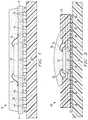
- Figure 1 is a cross-sectional illustration of an integrated circuit package according to the preferred embodiment of the present invention.
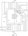
- Figure 2 is a plan view of the integrated circuit package according to Figure 1, including a cutaway portion.
- Figure 3 is a cross-sectional illustration of an integrated circuit package according to an alternative preferred embodiment of the present invention.
- packaged integrated circuit 8 according to a first preferred embodiment of the invention will now be described in detail. While packaged integrated circuit 8 according to this embodiment of the invention is shown in each of Figures 1 and 2 as already attached to system circuit board 20, it is to be understood by those of ordinary skill in the art that packaged integrated circuit 8 according to this embodiment of the invention will often individually manufactured and sold, with the purchaser performing the installation of packaged integrated circuit 8 to system circuit board 20 in a computer or other end equipment.
- the active element of packaged integrated circuit 8 is semiconductor chip 10, which is a solid-state integrated circuit device such as a microprocessor, memory, logic device, analog device or other electronic function implemented in a single-chip integrated circuit, as known in the art. According to this embodiment of the invention, chip 10 is attached on its bottom (inactive) surface to conductive slug 12, mounted within substrate 14.
- Substrate 14 may be a ceramic substrate, printed circuit board, or other similar substrate having conductors 24 thereupon or therewithin (see Figure 2) for carrying electrical signals to and from chip 10, and having an opening or receptacle therein within which conductive slug 12 is mounted.
- Bond wires 15 connect conductors 24 to bond pads on chip 10 in the conventional manner.
- Plated-through vias 19 make connection between conductors 24 on the top surface of substrate 14 and solder balls 18 on the lower surface of substrate 14.
- solder balls 18 are arranged in the conventional ball-grid-array manner, and correspond to lands or other surface conductors 23 (see Figure 2) on the top surface of system circuit board 20 to which packaged integrated circuit 8 is to be mounted.
- Conductive slug 12 is preferably formed of a material with high thermal conductivity, so that heat from chip 10 may be readily conducted therethrough. In addition, if electrical connection is to be made to the body of chip 10, conductive slug 12 is also preferably electrically conductive. The preferred material for conductive slug 12 is believed to be copper, but other materials known in the art to be thermally conductive and, if desired, electrically conductive, may alternatively be used for slug 12.
- Solder balls 18 are also disposed in an array manner beneath and in contact with slug 12, for providing thermal connection between slug 12 and a thermal conductor in system circuit board 20.
- conductive trace 22 is a wide trace on system circuit board 20 that is capable of conducting heat from chip 10 via slug 12 and solder balls 18.
- slug 12 may be connected by solder balls 18 to a ground plane within system circuit board 20. In either case, conductor 22 or the ground plane may be biased to ground or another substrate bias voltage, in which case slug 12 will also provide proper grounding for chip 10.
- packaged integrated circuit 8 begins with the insertion of slug 12 into the corresponding cavity of substrate 14; slug 12 is preferably epoxied into this cavity for mechanical integrity.
- Chip 10 is then mounted to the top surface of slug 12 by conventional die attach techniques, such as a conductive epoxy or eutectic mount.
- Bond wires 15 are then attached between substrate 14 and chip 10 by conventional techniques, such as thermocompression or ultrasonic bonding.
- encapsulant 16 is formed over chip 10 and wires 15 in the conventional manner.
- encapsulate 16 is formed by conventional transfer molding; alternatively, encapsulant 16 may be "globbed" over chip 10 and substrate 14 by dispensation and curing, in the conventional manner.
- Solder balls 18 are formed on the underside of substrate 14 and slug 12, in the conventional manner, for example by way of a solder mask (not shown) on the underside of substrate 14.
- packaged integrated circuit 8 Upon completion of the construction of packaged integrated circuit 8, and any desired electrical testing in packaged form, packaged integrated circuit 8 is ready for mounting to system circuit board 20. Mounting of packaged integrated circuit 8 is preferably done by way of wave soldering or other conventional technique for the surface mounting of BGA packages to circuit boards.
- Figure 3 illustrates, in cross-section, packaged integrated circuit 50 according to a second embodiment of the invention.
- packaged integrated circuit 50 includes chip 30 mounted upon thermally conductive slug 32.
- Slug 32 is disposed within substrate 34, which in this example is a multilayer circuit board including multiple levels of conductors therewithin.
- the multiple levels of conductors in substrate 34 are presented by multiple shells of lands, as indicated by the stepped arrangement near the chip cavity of substrate 34.
- a cutout is provided on the underside of substrate 34, to provide lateral surfaces 33 to which slug 32 may be epoxied or otherwise securely fastened.
- slug 32 includes a smaller portion protruding through substrate 34, to which chip 30 is mounted, with larger exposure on the underside of substrate 34.
- This construction allows for slug 32 to be the proper size for receipt of chip 30 on its top size, providing the maximum area for the arrangement of bond wire lands on substrate 34 with minimum wire length, while maximizing the surface area of thermal conduction on the underside.
- Bond wires 35 electrically connect conductors (not shown) in substrate 34 to pads on the surface of chip 30, for connection to the multiple planes of conductors.
- encapsulant 36 is disposed over the cavity of substrate 34, and thus over chip 30 and wires 35.
- Encapsulant 36 according to this embodiment of the invention is dispensed by way of a syringe or other liquid dispenser, and is then cured in the conventional manner for so-called "chip-on-board" construction.
- Solder balls 38 are attached to lands on the bottom surface of substrate 34. Vias (not shown) are provided within substrate 34 to provide electrical connection to the conductors in the substrate. Solder mask 37 on the underside of substrate 34 assists in defining the location of solder balls 38, during their formation in the conventional manner.
- packaged integrated circuit 50 is attached to system circuit board 40 by way of infrared (IR) solder reflow or other conventional surface mount technology.
- IR infrared
- Those solder balls 38 that are in contact with slug 32 connect to a thermal conductor within system circuit board 40, thus providing a path of relatively low thermal resistance between chip 30 and system circuit board 40 through solder balls 38 and slug 32.
- an integrated circuit package which has a high thermal conductivity path is provided between the active integrated circuit therewithin and the system circuit board to which the packaged integrated circuit is mounted.
- This enables the advantageous use of the system circuit board thermal conductivity to remove heat from the integrated circuit chip via conduction, and as such is suitable for use in zero-air-flow environments such as notebook-size computers, hand-held computing devices such as PDAs, and the like.
Abstract
Description
- This invention is in the field of semiconductor device packages, and is more particularly directed to thermal conduction techniques therein.
- Advances continue to be made in the manufacture of solid-state electronic devices, resulting in increasing functionality, density and performance of the integrated circuits. The amount of power dissipated, and accordingly the amount of heat generated, by modern integrated circuits generally increases with increases in the density and speed of the circuits. Removal of heat produced by the integrated circuits therefore continues to be of significant concern of modern integrated circuit package and system designers, considering the loss of performance and the degradation in reliability of integrated circuits when operated at elevated temperatures.
- In addition, the trend toward more compact electronic systems is also continuing, exacerbating the thermal problem produced by the high-complexity and high-performance integrated circuits. For example, laptop or notebook sized computers have recently become quite popular, with continuing market pressure toward even smaller computer systems such as personal digital assistants (PDAs). However, these small systems eliminate many of the techniques for heat removal available for large-scale computer systems, such as the use of fans for convection cooling of the integrated circuits. As such, many modern systems utilize thermal conduction as the primary mode of heat removal from the integrated circuits in the system.
- By way of further background, integrated circuit packages of the ball-grid-array (BGA) type have recently become popular in the field. Conventional BGA packages are similar in layout and arrangement to the pin-grid-array (PGA) packages, in providing a rectangular or square array of connections on the underside of the integrated circuit package. Instead of the pin connectors used in PGA packages, however, BGA packages utilize a solder ball located at each connector location. As is known in the art, the BGA package is attached to a printed circuit board by reflowing the solder balls to make connection to conductors at the surface of the printed circuit board. The BGA package provides the important advantage of being self-aligning, as the surface tension of the solder will tend to pull the BGA package into proper alignment with the corresponding conductors on the printed circuit board.
- By way of further background, BGA integrated circuit packages of various types are known, including those of both the "cavity-up" and the "cavity-down" type. Conventional cavity-up BGA,packages mount the integrated circuit chip face-up into a cavity (or onto the surface) of the package substrate, attach wire bonds between the package and the chip on this top side, and then either transfer mold or otherwise dispense a plastic over the chip and bond wires to provide environmental protection to the chip and wires. The solder balls are provided on the side of the substrate opposite the chip, and the packaged chip is then mounted to the system printed circuit board. It is known to use plated vias through the substrate at locations underlying the chip, but that are offset from conductors on the printed circuit board to which the packaged chip is mounted, to provide thermal conduction from the chip to its external environment.
- Conventional cavity-down integrated circuit packages mount the integrated circuit chip into the cavity of, or onto the surface of, the substrate, followed by attachment of bond wires thereto and molding of the plastic around the chip. In this type of package, the solder balls are provided on the same side of the substrate as the chip, so that the chip is disposed upside-down after attachment of the packaged chip to the circuit board. It is known to mount the chip to a thermally conductive slug disposed within the substrate of a cavity-down package, with the slug exposed on its opposite side from the chip after mounting. A heat sink may be mounted to the exposed upper surface of the slug, so that the heat sink extends upwardly and facilitates convection cooling. This arrangement is not particularly well suited for modern small computing systems, such as laptop, notebook-sized, or hand-held computers, as these systems are not able to house a fan, and indeed are designed to have no convection flow of air within the housing ("zero-air-flow").
- It is therefore an object of the present invention to provide an integrated circuit package having improved thermal conduction from the packaged chip to the circuit board upon which it is mounted.
- It is a further object of the present invention to provide such a package which is arranged in the cavity-up orientation.
- It is a further object of the present invention to provide such a package that is of the ball-grid-array (BGA) type.
- It is a further object of the present invention to provide such a package that reduces the need for convection cooling.
- Other objects and advantages of the present invention will be apparent to those of ordinary skill in the art having reference to the following specification together with its drawings.
- The invention may be implemented in a ball-grid-array (BGA) package of the cavity-up orientation. A thermally conductive slug, for example formed of copper, is inserted into a cavity of the package substrate; the substrate may itself be formed of a printed circuit board or ceramic substrate of the single, double, or multiple layer type. A surface of the slug is exposed on the underside of the substrate. The integrated circuit chip is attached to the slug, and bonds are made between the bond pads on the chip and the package conductors, followed by encapsulation of the chip by molding or dispensing of a plastic. Solder balls are attached on the underside of the package at locations corresponding to the terminals of the package, and also at locations on the exposed surface of the slug. Upon attachment to the system circuit board, thermal connection is made between the slug and system circuit board conductors, along with electrical connection of the other solder ball connectors to their respective system circuit board terminals. The slug thus provides direct thermal conduction between the chip and the system circuit board, to take advantage of the thermal conductivity of the system circuit board in conducting heat from the chip.
- Some embodiments of the invention Will now be described by way of example and with reference to the accompanying drawings in which:
- Figure 1 is a cross-sectional illustration of an integrated circuit package according to the preferred embodiment of the present invention.
- Figure 2 is a plan view of the integrated circuit package according to Figure 1, including a cutaway portion.
- Figure 3 is a cross-sectional illustration of an integrated circuit package according to an alternative preferred embodiment of the present invention.
- Referring now to Figures 1 and 2, packaged integrated
circuit 8 according to a first preferred embodiment of the invention will now be described in detail. While packagedintegrated circuit 8 according to this embodiment of the invention is shown in each of Figures 1 and 2 as already attached tosystem circuit board 20, it is to be understood by those of ordinary skill in the art that packagedintegrated circuit 8 according to this embodiment of the invention will often individually manufactured and sold, with the purchaser performing the installation of packaged integratedcircuit 8 tosystem circuit board 20 in a computer or other end equipment. - In addition, while the following description is provided using the example of a package containing a single integrated circuit chip, it is of course to be understood that the present invention is also applicable to the packaging or mounting of multiple integrated circuit chips to a board, for example in a hybrid integrated circuit or multichip module.
- The active element of packaged
integrated circuit 8 issemiconductor chip 10, which is a solid-state integrated circuit device such as a microprocessor, memory, logic device, analog device or other electronic function implemented in a single-chip integrated circuit, as known in the art. According to this embodiment of the invention,chip 10 is attached on its bottom (inactive) surface toconductive slug 12, mounted withinsubstrate 14. -
Substrate 14 may be a ceramic substrate, printed circuit board, or other similarsubstrate having conductors 24 thereupon or therewithin (see Figure 2) for carrying electrical signals to and fromchip 10, and having an opening or receptacle therein within whichconductive slug 12 is mounted.Bond wires 15 connectconductors 24 to bond pads onchip 10 in the conventional manner. Plated-throughvias 19 make connection betweenconductors 24 on the top surface ofsubstrate 14 andsolder balls 18 on the lower surface ofsubstrate 14. According to this embodiment of the invention,solder balls 18 are arranged in the conventional ball-grid-array manner, and correspond to lands or other surface conductors 23 (see Figure 2) on the top surface ofsystem circuit board 20 to which packagedintegrated circuit 8 is to be mounted. Encapsulant 16, formed of a plastic mold compound, an epoxy, a potting compound, or other conventional integrated circuit encapsulant, coverschip 10 andwires 15 to provide environmental and mechanical protection therefor. -
Conductive slug 12 is preferably formed of a material with high thermal conductivity, so that heat fromchip 10 may be readily conducted therethrough. In addition, if electrical connection is to be made to the body ofchip 10,conductive slug 12 is also preferably electrically conductive. The preferred material forconductive slug 12 is believed to be copper, but other materials known in the art to be thermally conductive and, if desired, electrically conductive, may alternatively be used forslug 12. -
Solder balls 18 are also disposed in an array manner beneath and in contact withslug 12, for providing thermal connection betweenslug 12 and a thermal conductor insystem circuit board 20. In the example of Figure 2,conductive trace 22 is a wide trace onsystem circuit board 20 that is capable of conducting heat fromchip 10 viaslug 12 andsolder balls 18. Alternatively, wheresystem circuit board 20 is of multilayer construction,slug 12 may be connected bysolder balls 18 to a ground plane withinsystem circuit board 20. In either case,conductor 22 or the ground plane may be biased to ground or another substrate bias voltage, in whichcase slug 12 will also provide proper grounding forchip 10. - The fabrication of packaged integrated
circuit 8 begins with the insertion ofslug 12 into the corresponding cavity ofsubstrate 14;slug 12 is preferably epoxied into this cavity for mechanical integrity.Chip 10 is then mounted to the top surface ofslug 12 by conventional die attach techniques, such as a conductive epoxy or eutectic mount.Bond wires 15 are then attached betweensubstrate 14 andchip 10 by conventional techniques, such as thermocompression or ultrasonic bonding. Upon completion of the wire bond process,encapsulant 16 is formed overchip 10 andwires 15 in the conventional manner. In the example of Figures 1 and 2,encapsulate 16 is formed by conventional transfer molding; alternatively, encapsulant 16 may be "globbed" overchip 10 andsubstrate 14 by dispensation and curing, in the conventional manner.Solder balls 18 are formed on the underside ofsubstrate 14 andslug 12, in the conventional manner, for example by way of a solder mask (not shown) on the underside ofsubstrate 14. - Upon completion of the construction of packaged
integrated circuit 8, and any desired electrical testing in packaged form, packagedintegrated circuit 8 is ready for mounting tosystem circuit board 20. Mounting of packaged integratedcircuit 8 is preferably done by way of wave soldering or other conventional technique for the surface mounting of BGA packages to circuit boards. - Figure 3 illustrates, in cross-section, packaged
integrated circuit 50 according to a second embodiment of the invention. According to this embodiment of the invention, packaged integratedcircuit 50 includeschip 30 mounted upon thermallyconductive slug 32.Slug 32 is disposed withinsubstrate 34, which in this example is a multilayer circuit board including multiple levels of conductors therewithin. The multiple levels of conductors insubstrate 34 are presented by multiple shells of lands, as indicated by the stepped arrangement near the chip cavity ofsubstrate 34. A cutout is provided on the underside ofsubstrate 34, to providelateral surfaces 33 to whichslug 32 may be epoxied or otherwise securely fastened. In this arrangement, slug 32 includes a smaller portion protruding throughsubstrate 34, to whichchip 30 is mounted, with larger exposure on the underside ofsubstrate 34. This construction allows forslug 32 to be the proper size for receipt ofchip 30 on its top size, providing the maximum area for the arrangement of bond wire lands onsubstrate 34 with minimum wire length, while maximizing the surface area of thermal conduction on the underside. -
Bond wires 35 electrically connect conductors (not shown) insubstrate 34 to pads on the surface ofchip 30, for connection to the multiple planes of conductors. In this embodiment of the invention,encapsulant 36 is disposed over the cavity ofsubstrate 34, and thus overchip 30 andwires 35.Encapsulant 36 according to this embodiment of the invention is dispensed by way of a syringe or other liquid dispenser, and is then cured in the conventional manner for so-called "chip-on-board" construction. -
Solder balls 38 are attached to lands on the bottom surface ofsubstrate 34. Vias (not shown) are provided withinsubstrate 34 to provide electrical connection to the conductors in the substrate.Solder mask 37 on the underside ofsubstrate 34 assists in defining the location ofsolder balls 38, during their formation in the conventional manner. - As in the first embodiment discussed hereinabove, packaged integrated
circuit 50 is attached tosystem circuit board 40 by way of infrared (IR) solder reflow or other conventional surface mount technology. Thosesolder balls 38 that are in contact withslug 32 connect to a thermal conductor withinsystem circuit board 40, thus providing a path of relatively low thermal resistance betweenchip 30 andsystem circuit board 40 throughsolder balls 38 andslug 32. - According to each of these embodiments of the invention, an integrated circuit package is provided which has a high thermal conductivity path is provided between the active integrated circuit therewithin and the system circuit board to which the packaged integrated circuit is mounted. This enables the advantageous use of the system circuit board thermal conductivity to remove heat from the integrated circuit chip via conduction, and as such is suitable for use in zero-air-flow environments such as notebook-size computers, hand-held computing devices such as PDAs, and the like.
- While the invention has been described herein relative to its preferred embodiments, it is of course contemplated that modifications of, and alternatives to, these embodiments, such modifications and alternatives obtaining the advantages and benefits of this invention, will be apparent to those of ordinary skill in the art having reference to this specification and its drawings. It is contemplated that such modifications and alternatives are within the scope of this invention as subsequently claimed herein.
Claims (17)
- A packaged integrated circuit, comprising:
a substrate having first and second surfaces, having a opening disposed therethrough, and having a plurality of electrical conductors;
a slug, comprised of a thermally conductive material and having first and second surfaces, said slug extending through the opening of said substrate so that its first surface is exposed at said first surface of said substrate;
an integrated circuit chip, mounted to the second surface of said slug, and electrically connected to the conductors of said substrate;
a plurality of electrical connectors, disposed at the first surface of said substrate, and in electrical connection with the conductors of said substrate, said plurality of electrical connectors for making connection to a circuit board; and
a thermal conductor, disposed at the first surface of said slug, for making thermal connection to the circuit board. - The packaged integrated circuit of claim 1, wherein said plurality of electrical connectors comprise a plurality of solder balls.
- The packaged integrated circuit of claim 2, wherein said thermal conductor comprises a plurality of solder balls.
- The packaged integrated circuit of claim 1, further comprising:
an encapsulant, disposed over said integrated circuit chip and over a portion of the second surface of said substrate. - The packaged integrated circuit of claim 4, wherein said encapsulant comprises molded plastic.
- The packaged integrated circuit of claim 1, wherein said substrate comprises a printed circuit board.
- The packaged integrated circuit of claim 6, wherein said printed circuit board is of the multilayer type.
- The packaged integrated circuit of claim 1, wherein said substrate comprises a ceramic substrate.
- The packaged integrated circuit of claim 8, wherein said ceramic substrate is of the multilayer type.
- The packaged integrated circuit of claim 1, wherein said slug comprises copper.
- The packaged integrated circuit of claim 1, wherein the first surface of said slug has a surface area greater than the second surface of said slug.
- A method of fabricating a packaged integrated circuit, comprising:
inserting a thermally conductive slug into a substrate having first and second opposing surfaces, said thermally conductive slug having a first surface exposed at the first surface of the substrate, and having a second surface opposite therefrom;
mounting an integrated circuit chip to the second surface of the thermally conductive slug;
encapsulating said integrated circuit chip;
attaching electrical connectors to the substrate at its first surface; and
attaching a thermal conductor to the slug at its first surface. - The method of claim 12, wherein the step of attaching electrical connectors to the substrate comprises attaching solder balls to the substrate at its first surface.
- The method of claim 13, wherein the step of attaching a thermal conductor to the slug comprises attaching solder balls to the slug at its first surface.
- The method of claim 12, wherein the encapsulating step comprises:
transfer molding a plastic mold compound over said chip. - The method of claim 12, wherein the encapsulating step comprises:
dispensing a plastic over said chip; and
curing the dispensed plastic. - The method of claim 12, wherein the step of attaching electrical connectors to the substrate and the step of attaching a thermal conductor to the slug comprise attaching solder balls to the substrate and to the slug at their respective first surfaces;
and further comprising:
attaching the packaged integrated circuit to a circuit board.
Applications Claiming Priority (2)
| Application Number | Priority Date | Filing Date | Title |
|---|---|---|---|
| US17061393A | 1993-12-20 | 1993-12-20 | |
| US170613 | 1993-12-20 |
Publications (2)
| Publication Number | Publication Date |
|---|---|
| EP0660399A2 true EP0660399A2 (en) | 1995-06-28 |
| EP0660399A3 EP0660399A3 (en) | 1995-07-26 |
Family
ID=22620603
Family Applications (1)
| Application Number | Title | Priority Date | Filing Date |
|---|---|---|---|
| EP94308577A Withdrawn EP0660399A2 (en) | 1993-12-20 | 1994-11-21 | Ball-grid-array integrated circuit package with thermal conductivity |
Country Status (3)
| Country | Link |
|---|---|
| US (2) | US5991156A (en) |
| EP (1) | EP0660399A2 (en) |
| JP (1) | JPH07211816A (en) |
Cited By (4)
| Publication number | Priority date | Publication date | Assignee | Title |
|---|---|---|---|---|
| EP0690500A1 (en) * | 1994-06-30 | 1996-01-03 | STMicroelectronics, Inc. | Ball-grid-array integrated circuit package with solder-connected thermal conductor |
| WO1997026605A1 (en) * | 1996-01-22 | 1997-07-24 | Silicon Graphics, Inc. | Processor-inclusive memory module |
| US5867419A (en) * | 1997-01-27 | 1999-02-02 | Silicon Graphics, Inc. | Processor-inclusive memory module |
| EP3706165A1 (en) * | 2019-03-04 | 2020-09-09 | INTEL Corporation | Nested architectures for enhanced heterogeneous integration |
Families Citing this family (74)
| Publication number | Priority date | Publication date | Assignee | Title |
|---|---|---|---|---|
| TW344109B (en) * | 1994-02-10 | 1998-11-01 | Hitachi Ltd | Methods of making semiconductor devices |
| US6686226B1 (en) | 1994-02-10 | 2004-02-03 | Hitachi, Ltd. | Method of manufacturing a semiconductor device a ball grid array package structure using a supporting frame |
| NL9500238A (en) * | 1995-02-09 | 1996-09-02 | Fico Bv | Casing device with compensation element. |
| JP3793628B2 (en) * | 1997-01-20 | 2006-07-05 | 沖電気工業株式会社 | Resin-sealed semiconductor device |
| DE19750306A1 (en) * | 1997-11-13 | 1999-05-20 | Bosch Gmbh Robert | Electronic control device for motor vehicle |
| US6060777A (en) * | 1998-07-21 | 2000-05-09 | Intel Corporation | Underside heat slug for ball grid array packages |
| US6424034B1 (en) * | 1998-08-31 | 2002-07-23 | Micron Technology, Inc. | High performance packaging for microprocessors and DRAM chips which minimizes timing skews |
| JP4142170B2 (en) * | 1998-09-25 | 2008-08-27 | 新電元工業株式会社 | Electrical equipment |
| US6138894A (en) * | 1998-11-25 | 2000-10-31 | Intermedics Inc. | Method for coupling a circuit component to a substrate |
| US6321175B1 (en) * | 1998-12-21 | 2001-11-20 | Intel Corporation | Thermal sensing of multiple integrated circuits |
| US6844253B2 (en) | 1999-02-19 | 2005-01-18 | Micron Technology, Inc. | Selective deposition of solder ball contacts |
| US6435396B1 (en) * | 2000-04-10 | 2002-08-20 | Micron Technology, Inc. | Print head for ejecting liquid droplets |
| US6878396B2 (en) | 2000-04-10 | 2005-04-12 | Micron Technology, Inc. | Micro C-4 semiconductor die and method for depositing connection sites thereon |
| US6249434B1 (en) | 2000-06-20 | 2001-06-19 | Adc Telecommunications, Inc. | Surface mounted conduction heat sink |
| US6734552B2 (en) * | 2001-07-11 | 2004-05-11 | Asat Limited | Enhanced thermal dissipation integrated circuit package |
| US7015072B2 (en) | 2001-07-11 | 2006-03-21 | Asat Limited | Method of manufacturing an enhanced thermal dissipation integrated circuit package |
| WO2003017328A2 (en) * | 2001-08-15 | 2003-02-27 | Asat Limited | Encapsulated integrated circuit package and method of manufacturing an integrated circuit package |
| US6790710B2 (en) | 2002-01-31 | 2004-09-14 | Asat Limited | Method of manufacturing an integrated circuit package |
| US6787895B1 (en) * | 2001-12-07 | 2004-09-07 | Skyworks Solutions, Inc. | Leadless chip carrier for reduced thermal resistance |
| EP1353375A1 (en) * | 2002-04-10 | 2003-10-15 | United Test Center Inc. | A thermally enhanced IC chip package |
| US6940154B2 (en) * | 2002-06-24 | 2005-09-06 | Asat Limited | Integrated circuit package and method of manufacturing the integrated circuit package |
| US6998721B2 (en) * | 2002-11-08 | 2006-02-14 | Stmicroelectronics, Inc. | Stacking and encapsulation of multiple interconnected integrated circuits |
| US6781242B1 (en) * | 2002-12-02 | 2004-08-24 | Asat, Ltd. | Thin ball grid array package |
| US7126210B2 (en) * | 2003-04-02 | 2006-10-24 | Stmicroelectronics, Inc. | System and method for venting pressure from an integrated circuit package sealed with a lid |
| US20070031996A1 (en) * | 2003-04-26 | 2007-02-08 | Chopin Sheila F | Packaged integrated circuit having a heat spreader and method therefor |
| US6849944B2 (en) * | 2003-05-30 | 2005-02-01 | Texas Instruments Incorporated | Using a supporting structure to control collapse of a die towards a die pad during a reflow process for coupling the die to the die pad |
| US20040245624A1 (en) * | 2003-06-03 | 2004-12-09 | Swanson Leland S. | Using solder balls of multiple sizes to couple one or more semiconductor structures to an electrical device |
| US7347349B2 (en) * | 2003-06-24 | 2008-03-25 | Micron Technology, Inc. | Apparatus and method for printing micro metal structures |
| US20040264195A1 (en) * | 2003-06-25 | 2004-12-30 | Chia-Fu Chang | Led light source having a heat sink |
| US7084500B2 (en) * | 2003-10-29 | 2006-08-01 | Texas Instruments Incorporated | Semiconductor circuit with multiple contact sizes |
| US7830011B2 (en) * | 2004-03-15 | 2010-11-09 | Yamaha Corporation | Semiconductor element and wafer level chip size package therefor |
| WO2005114730A1 (en) * | 2004-05-20 | 2005-12-01 | Spansion Llc | Process for producing semiconductor device and semiconductor device |
| US8164182B2 (en) * | 2004-11-15 | 2012-04-24 | Stats Chippac Ltd. | Hyper thermally enhanced semiconductor package system comprising heat slugs on opposite surfaces of a semiconductor chip |
| US7433192B2 (en) * | 2004-12-29 | 2008-10-07 | Agere Systems Inc. | Packaging for electronic modules |
| US7215204B2 (en) * | 2004-12-29 | 2007-05-08 | Agere Systems Inc. | Intelligent high-power amplifier module |
| US20080083981A1 (en) * | 2006-06-07 | 2008-04-10 | Romig Matthew D | Thermally Enhanced BGA Packages and Methods |
| US7903425B2 (en) * | 2006-06-27 | 2011-03-08 | Lenovo (Singapore) Pte. Ltd. | Integrated circuit chip thermal solution |
| US7554194B2 (en) * | 2006-11-08 | 2009-06-30 | Amkor Technology, Inc. | Thermally enhanced semiconductor package |
| US8450842B2 (en) * | 2007-03-20 | 2013-05-28 | Kyocera Corporation | Structure and electronics device using the structure |
| US8329510B2 (en) * | 2008-03-25 | 2012-12-11 | Bridge Semiconductor Corporation | Method of making a semiconductor chip assembly with a post/base heat spreader with an ESD protection layer |
| US20100052005A1 (en) * | 2008-03-25 | 2010-03-04 | Lin Charles W C | Semiconductor chip assembly with post/base heat spreader and conductive trace |
| US8067784B2 (en) | 2008-03-25 | 2011-11-29 | Bridge Semiconductor Corporation | Semiconductor chip assembly with post/base heat spreader and substrate |
| US8314438B2 (en) * | 2008-03-25 | 2012-11-20 | Bridge Semiconductor Corporation | Semiconductor chip assembly with bump/base heat spreader and cavity in bump |
| US8232576B1 (en) | 2008-03-25 | 2012-07-31 | Bridge Semiconductor Corporation | Semiconductor chip assembly with post/base heat spreader and ceramic block in post |
| US8207553B2 (en) * | 2008-03-25 | 2012-06-26 | Bridge Semiconductor Corporation | Semiconductor chip assembly with base heat spreader and cavity in base |
| US8269336B2 (en) * | 2008-03-25 | 2012-09-18 | Bridge Semiconductor Corporation | Semiconductor chip assembly with post/base heat spreader and signal post |
| US8531024B2 (en) * | 2008-03-25 | 2013-09-10 | Bridge Semiconductor Corporation | Semiconductor chip assembly with post/base heat spreader and multilevel conductive trace |
| US8203167B2 (en) * | 2008-03-25 | 2012-06-19 | Bridge Semiconductor Corporation | Semiconductor chip assembly with post/base heat spreader and adhesive between base and terminal |
| US8415703B2 (en) * | 2008-03-25 | 2013-04-09 | Bridge Semiconductor Corporation | Semiconductor chip assembly with post/base/flange heat spreader and cavity in flange |
| US8148747B2 (en) * | 2008-03-25 | 2012-04-03 | Bridge Semiconductor Corporation | Semiconductor chip assembly with post/base/cap heat spreader |
| US8129742B2 (en) * | 2008-03-25 | 2012-03-06 | Bridge Semiconductor Corporation | Semiconductor chip assembly with post/base heat spreader and plated through-hole |
| US8288792B2 (en) * | 2008-03-25 | 2012-10-16 | Bridge Semiconductor Corporation | Semiconductor chip assembly with post/base/post heat spreader |
| US8525214B2 (en) * | 2008-03-25 | 2013-09-03 | Bridge Semiconductor Corporation | Semiconductor chip assembly with post/base heat spreader with thermal via |
| US20110278638A1 (en) | 2008-03-25 | 2011-11-17 | Lin Charles W C | Semiconductor chip assembly with post/dielectric/post heat spreader |
| US8310043B2 (en) * | 2008-03-25 | 2012-11-13 | Bridge Semiconductor Corporation | Semiconductor chip assembly with post/base heat spreader with ESD protection layer |
| US8324723B2 (en) * | 2008-03-25 | 2012-12-04 | Bridge Semiconductor Corporation | Semiconductor chip assembly with bump/base heat spreader and dual-angle cavity in bump |
| US20090284932A1 (en) * | 2008-03-25 | 2009-11-19 | Bridge Semiconductor Corporation | Thermally Enhanced Package with Embedded Metal Slug and Patterned Circuitry |
| US8354688B2 (en) | 2008-03-25 | 2013-01-15 | Bridge Semiconductor Corporation | Semiconductor chip assembly with bump/base/ledge heat spreader, dual adhesives and cavity in bump |
| US8378372B2 (en) * | 2008-03-25 | 2013-02-19 | Bridge Semiconductor Corporation | Semiconductor chip assembly with post/base heat spreader and horizontal signal routing |
| US20100181594A1 (en) * | 2008-03-25 | 2010-07-22 | Lin Charles W C | Semiconductor chip assembly with post/base heat spreader and cavity over post |
| US8212279B2 (en) * | 2008-03-25 | 2012-07-03 | Bridge Semiconductor Corporation | Semiconductor chip assembly with post/base heat spreader, signal post and cavity |
| US20110156090A1 (en) * | 2008-03-25 | 2011-06-30 | Lin Charles W C | Semiconductor chip assembly with post/base/post heat spreader and asymmetric posts |
| US9018667B2 (en) * | 2008-03-25 | 2015-04-28 | Bridge Semiconductor Corporation | Semiconductor chip assembly with post/base heat spreader and dual adhesives |
| US8193556B2 (en) * | 2008-03-25 | 2012-06-05 | Bridge Semiconductor Corporation | Semiconductor chip assembly with post/base heat spreader and cavity in post |
| US20110163348A1 (en) * | 2008-03-25 | 2011-07-07 | Bridge Semiconductor Corporation | Semiconductor chip assembly with bump/base heat spreader and inverted cavity in bump |
| US20100019374A1 (en) * | 2008-07-25 | 2010-01-28 | Stmicroelectronics, Inc. | Ball grid array package |
| US8324653B1 (en) | 2009-08-06 | 2012-12-04 | Bridge Semiconductor Corporation | Semiconductor chip assembly with ceramic/metal substrate |
| JP5271886B2 (en) * | 2009-12-08 | 2013-08-21 | ルネサスエレクトロニクス株式会社 | Semiconductor device and manufacturing method thereof |
| JP5858637B2 (en) * | 2011-04-14 | 2016-02-10 | 三菱電機株式会社 | Semiconductor package |
| CN102403418A (en) * | 2011-11-09 | 2012-04-04 | 东莞勤上光电股份有限公司 | Manufacturing method of high-power LED radiating structure |
| US20130308274A1 (en) * | 2012-05-21 | 2013-11-21 | Triquint Semiconductor, Inc. | Thermal spreader having graduated thermal expansion parameters |
| TWI605557B (en) * | 2015-12-31 | 2017-11-11 | 矽品精密工業股份有限公司 | Electronic package, method for fabricating the electronic package, and substrate structure |
| TWI692846B (en) * | 2019-03-21 | 2020-05-01 | 旭德科技股份有限公司 | Heat dissipation substrate and fabricating method thereof |
| CN111416269B (en) * | 2020-03-30 | 2021-09-10 | 武汉光谷信息光电子创新中心有限公司 | Light emitting device |
Citations (6)
| Publication number | Priority date | Publication date | Assignee | Title |
|---|---|---|---|---|
| EP0272390A2 (en) * | 1986-11-25 | 1988-06-29 | Kabushiki Kaisha Toshiba | Packages for a semiconductor device |
| FR2609841A1 (en) * | 1987-01-20 | 1988-07-22 | Toshiba Kk | SEMICONDUCTOR INTEGRATED CIRCUIT DEVICE |
| US5157480A (en) * | 1991-02-06 | 1992-10-20 | Motorola, Inc. | Semiconductor device having dual electrical contact sites |
| US5216278A (en) * | 1990-12-04 | 1993-06-01 | Motorola, Inc. | Semiconductor device having a pad array carrier package |
| DE9308842U1 (en) * | 1993-06-14 | 1993-07-22 | Blaupunkt-Werke Gmbh, 31139 Hildesheim, De | |
| US5285352A (en) * | 1992-07-15 | 1994-02-08 | Motorola, Inc. | Pad array semiconductor device with thermal conductor and process for making the same |
Family Cites Families (22)
| Publication number | Priority date | Publication date | Assignee | Title |
|---|---|---|---|---|
| JPS63120431A (en) * | 1986-11-10 | 1988-05-24 | Nec Corp | Semiconductor device for electric power |
| JPS63293965A (en) * | 1987-05-27 | 1988-11-30 | Hitachi Ltd | Semiconductor device and manufacture thereof |
| JP2660295B2 (en) * | 1988-08-24 | 1997-10-08 | イビデン株式会社 | Substrate for mounting electronic components |
| DE69018846T2 (en) * | 1989-02-10 | 1995-08-24 | Fujitsu Ltd | Semiconductor device type ceramic package and method of assembling the same. |
| US5266834A (en) * | 1989-03-13 | 1993-11-30 | Hitachi Ltd. | Semiconductor device and an electronic device with the semiconductor devices mounted thereon |
| US5041396A (en) * | 1989-07-18 | 1991-08-20 | Vlsi Technology, Inc. | Reusable package for holding a semiconductor chip and method for reusing the package |
| US5012386A (en) * | 1989-10-27 | 1991-04-30 | Motorola, Inc. | High performance overmolded electronic package |
| JPH03198368A (en) * | 1989-12-26 | 1991-08-29 | Nec Corp | Semiconductor device |
| US5202288A (en) * | 1990-06-01 | 1993-04-13 | Robert Bosch Gmbh | Method of manufacturing an electronic circuit component incorporating a heat sink |
| US5293072A (en) * | 1990-06-25 | 1994-03-08 | Fujitsu Limited | Semiconductor device having spherical terminals attached to the lead frame embedded within the package body |
| US5120678A (en) * | 1990-11-05 | 1992-06-09 | Motorola Inc. | Electrical component package comprising polymer-reinforced solder bump interconnection |
| US5102829A (en) * | 1991-07-22 | 1992-04-07 | At&T Bell Laboratories | Plastic pin grid array package |
| US5172301A (en) * | 1991-10-08 | 1992-12-15 | Lsi Logic Corporation | Heatsink for board-mounted semiconductor devices and semiconductor device assembly employing same |
| JP2602380B2 (en) * | 1991-10-23 | 1997-04-23 | 富士通株式会社 | Semiconductor device and manufacturing method thereof |
| CA2089435C (en) * | 1992-02-14 | 1997-12-09 | Kenzi Kobayashi | Semiconductor device |
| US5222014A (en) * | 1992-03-02 | 1993-06-22 | Motorola, Inc. | Three-dimensional multi-chip pad array carrier |
| JP3174393B2 (en) * | 1992-04-24 | 2001-06-11 | シチズン時計株式会社 | Manufacturing method of electronic component mounting board |
| JPH06295962A (en) * | 1992-10-20 | 1994-10-21 | Ibiden Co Ltd | Electronic part mounting substrate and manufacture thereof as well as electronic part mounting device |
| US5291062A (en) * | 1993-03-01 | 1994-03-01 | Motorola, Inc. | Area array semiconductor device having a lid with functional contacts |
| US5474958A (en) * | 1993-05-04 | 1995-12-12 | Motorola, Inc. | Method for making semiconductor device having no die supporting surface |
| US5362679A (en) * | 1993-07-26 | 1994-11-08 | Vlsi Packaging Corporation | Plastic package with solder grid array |
| US5455456A (en) * | 1993-09-15 | 1995-10-03 | Lsi Logic Corporation | Integrated circuit package lid |
-
1994
- 1994-04-08 US US08/225,138 patent/US5991156A/en not_active Expired - Lifetime
- 1994-11-21 EP EP94308577A patent/EP0660399A2/en not_active Withdrawn
- 1994-12-20 JP JP6316867A patent/JPH07211816A/en active Pending
-
1996
- 1996-01-18 US US08/588,340 patent/US5693572A/en not_active Expired - Lifetime
Patent Citations (6)
| Publication number | Priority date | Publication date | Assignee | Title |
|---|---|---|---|---|
| EP0272390A2 (en) * | 1986-11-25 | 1988-06-29 | Kabushiki Kaisha Toshiba | Packages for a semiconductor device |
| FR2609841A1 (en) * | 1987-01-20 | 1988-07-22 | Toshiba Kk | SEMICONDUCTOR INTEGRATED CIRCUIT DEVICE |
| US5216278A (en) * | 1990-12-04 | 1993-06-01 | Motorola, Inc. | Semiconductor device having a pad array carrier package |
| US5157480A (en) * | 1991-02-06 | 1992-10-20 | Motorola, Inc. | Semiconductor device having dual electrical contact sites |
| US5285352A (en) * | 1992-07-15 | 1994-02-08 | Motorola, Inc. | Pad array semiconductor device with thermal conductor and process for making the same |
| DE9308842U1 (en) * | 1993-06-14 | 1993-07-22 | Blaupunkt-Werke Gmbh, 31139 Hildesheim, De |
Non-Patent Citations (1)
| Title |
|---|
| PATENT ABSTRACTS OF JAPAN vol. 018 no. 105 (E-1512) ,21 February 1994 & JP-A-05 304223 (CITIZEN WATCH CO LTD) 16 November 1993, * |
Cited By (9)
| Publication number | Priority date | Publication date | Assignee | Title |
|---|---|---|---|---|
| US5642261A (en) * | 1993-12-20 | 1997-06-24 | Sgs-Thomson Microelectronics, Inc. | Ball-grid-array integrated circuit package with solder-connected thermal conductor |
| EP0690500A1 (en) * | 1994-06-30 | 1996-01-03 | STMicroelectronics, Inc. | Ball-grid-array integrated circuit package with solder-connected thermal conductor |
| WO1997026605A1 (en) * | 1996-01-22 | 1997-07-24 | Silicon Graphics, Inc. | Processor-inclusive memory module |
| US5710733A (en) * | 1996-01-22 | 1998-01-20 | Silicon Graphics, Inc. | Processor-inclusive memory module |
| US5999437A (en) * | 1996-01-22 | 1999-12-07 | Silicon Graphics, Inc. | Processor-inclusive memory module |
| US5867419A (en) * | 1997-01-27 | 1999-02-02 | Silicon Graphics, Inc. | Processor-inclusive memory module |
| EP3706165A1 (en) * | 2019-03-04 | 2020-09-09 | INTEL Corporation | Nested architectures for enhanced heterogeneous integration |
| US11742261B2 (en) | 2019-03-04 | 2023-08-29 | Intel Corporation | Nested architectures for enhanced heterogeneous integration |
| US11798865B2 (en) | 2019-03-04 | 2023-10-24 | Intel Corporation | Nested architectures for enhanced heterogeneous integration |
Also Published As
| Publication number | Publication date |
|---|---|
| JPH07211816A (en) | 1995-08-11 |
| US5991156A (en) | 1999-11-23 |
| US5693572A (en) | 1997-12-02 |
| EP0660399A3 (en) | 1995-07-26 |
Similar Documents
| Publication | Publication Date | Title |
|---|---|---|
| EP0690500B1 (en) | Ball-grid-array integrated circuit package with solder-connected thermal conductor | |
| EP0660399A2 (en) | Ball-grid-array integrated circuit package with thermal conductivity | |
| KR100694739B1 (en) | Ball grid array package with multiple power/ground planes | |
| US5977626A (en) | Thermally and electrically enhanced PBGA package | |
| US5291062A (en) | Area array semiconductor device having a lid with functional contacts | |
| JP4476482B2 (en) | Low profile ball grid array semiconductor package, integrated circuit, printed circuit board, processor system, method for manufacturing low profile ball grid array semiconductor package, and method for mounting semiconductor die | |
| US6146921A (en) | Cavity mold cap BGA package with post mold thermally conductive epoxy attach heat sink | |
| US5705851A (en) | Thermal ball lead integrated package | |
| US6853069B2 (en) | Packaged die on PCB with heat sink encapsulant and methods | |
| US5777345A (en) | Multi-chip integrated circuit package | |
| US5302849A (en) | Plastic and grid array semiconductor device and method for making the same | |
| US6507107B2 (en) | Semiconductor/printed circuit board assembly | |
| KR0169820B1 (en) | Chip scale package with metal wiring substrate | |
| JPH09153565A (en) | Ball grid array package with heat sink | |
| US6894229B1 (en) | Mechanically enhanced package and method of making same | |
| US7344916B2 (en) | Package for a semiconductor device | |
| KR100995478B1 (en) | Packaged semiconductor device and method of formation | |
| JP3148718B2 (en) | Thermally and electrically enhanced semiconductor package | |
| EP0676806B1 (en) | Ball grid array intergrated circuit package with high thermal conductivity | |
| KR100230189B1 (en) | Ball grid array semiconductor package | |
| US6963129B1 (en) | Multi-chip package having a contiguous heat spreader assembly | |
| KR100230919B1 (en) | Semiconductor package | |
| KR20000018896A (en) | Thermally and electrically improved pbga package |
Legal Events
| Date | Code | Title | Description |
|---|---|---|---|
| PUAI | Public reference made under article 153(3) epc to a published international application that has entered the european phase |
Free format text: ORIGINAL CODE: 0009012 |
|
| PUAL | Search report despatched |
Free format text: ORIGINAL CODE: 0009013 |
|
| AK | Designated contracting states |
Kind code of ref document: A2 Designated state(s): DE FR GB IT |
|
| AK | Designated contracting states |
Kind code of ref document: A3 Designated state(s): DE FR GB IT |
|
| 17P | Request for examination filed |
Effective date: 19960115 |
|
| 17Q | First examination report despatched |
Effective date: 19961113 |
|
| RAP3 | Party data changed (applicant data changed or rights of an application transferred) |
Owner name: STMICROELECTRONICS, INC. |
|
| STAA | Information on the status of an ep patent application or granted ep patent |
Free format text: STATUS: THE APPLICATION HAS BEEN WITHDRAWN |
|
| 18W | Application withdrawn |
Withdrawal date: 19990126 |