EP0645950B1 - Connecting member of a circuit substrate and method of manufacturing multilayer circuit substrates by using the same - Google Patents
Connecting member of a circuit substrate and method of manufacturing multilayer circuit substrates by using the same Download PDFInfo
- Publication number
- EP0645950B1 EP0645950B1 EP19940114796 EP94114796A EP0645950B1 EP 0645950 B1 EP0645950 B1 EP 0645950B1 EP 19940114796 EP19940114796 EP 19940114796 EP 94114796 A EP94114796 A EP 94114796A EP 0645950 B1 EP0645950 B1 EP 0645950B1
- Authority
- EP
- European Patent Office
- Prior art keywords
- connecting member
- base material
- holes
- porous base
- circuit substrate
- Prior art date
- Legal status (The legal status is an assumption and is not a legal conclusion. Google has not performed a legal analysis and makes no representation as to the accuracy of the status listed.)
- Expired - Lifetime
Links
- 239000000758 substrate Substances 0.000 title claims description 253
- 238000004519 manufacturing process Methods 0.000 title claims description 34
- 229920005989 resin Polymers 0.000 claims description 96
- 239000011347 resin Substances 0.000 claims description 96
- 238000000034 method Methods 0.000 claims description 77
- 239000000463 material Substances 0.000 claims description 68
- 229920001187 thermosetting polymer Polymers 0.000 claims description 40
- 150000001875 compounds Chemical class 0.000 claims description 38
- 239000004593 Epoxy Substances 0.000 claims description 37
- RYGMFSIKBFXOCR-UHFFFAOYSA-N Copper Chemical compound [Cu] RYGMFSIKBFXOCR-UHFFFAOYSA-N 0.000 claims description 36
- 239000003822 epoxy resin Substances 0.000 claims description 36
- 229920000647 polyepoxide Polymers 0.000 claims description 36
- 239000002184 metal Substances 0.000 claims description 24
- 229910052751 metal Inorganic materials 0.000 claims description 24
- 238000010438 heat treatment Methods 0.000 claims description 22
- 239000011889 copper foil Substances 0.000 claims description 21
- 239000011888 foil Substances 0.000 claims description 20
- 239000000126 substance Substances 0.000 claims description 20
- 239000010949 copper Substances 0.000 claims description 15
- 229920003235 aromatic polyamide Polymers 0.000 claims description 14
- 239000004744 fabric Substances 0.000 claims description 14
- 239000004760 aramid Substances 0.000 claims description 13
- 239000002131 composite material Substances 0.000 claims description 13
- 239000004745 nonwoven fabric Substances 0.000 claims description 13
- PXHVJJICTQNCMI-UHFFFAOYSA-N Nickel Chemical compound [Ni] PXHVJJICTQNCMI-UHFFFAOYSA-N 0.000 claims description 12
- 229910052802 copper Inorganic materials 0.000 claims description 9
- 229920002994 synthetic fiber Polymers 0.000 claims description 9
- 239000012209 synthetic fiber Substances 0.000 claims description 9
- BQCADISMDOOEFD-UHFFFAOYSA-N Silver Chemical compound [Ag] BQCADISMDOOEFD-UHFFFAOYSA-N 0.000 claims description 7
- 229910052709 silver Inorganic materials 0.000 claims description 6
- 239000004332 silver Substances 0.000 claims description 6
- 229910052759 nickel Inorganic materials 0.000 claims description 5
- 239000000843 powder Substances 0.000 claims description 5
- 239000005011 phenolic resin Substances 0.000 claims description 3
- 238000000926 separation method Methods 0.000 claims description 2
- 229910001316 Ag alloy Inorganic materials 0.000 claims 1
- 229910000881 Cu alloy Inorganic materials 0.000 claims 1
- 229910000990 Ni alloy Inorganic materials 0.000 claims 1
- 239000010410 layer Substances 0.000 description 55
- 239000011521 glass Substances 0.000 description 27
- 230000008569 process Effects 0.000 description 17
- 238000012360 testing method Methods 0.000 description 17
- 238000007598 dipping method Methods 0.000 description 15
- 230000002787 reinforcement Effects 0.000 description 14
- 239000004848 polyfunctional curative Substances 0.000 description 13
- 239000000123 paper Substances 0.000 description 12
- 229910000679 solder Inorganic materials 0.000 description 10
- 239000002759 woven fabric Substances 0.000 description 10
- 238000007747 plating Methods 0.000 description 9
- 238000012545 processing Methods 0.000 description 9
- 238000003825 pressing Methods 0.000 description 8
- 239000011231 conductive filler Substances 0.000 description 7
- 239000002904 solvent Substances 0.000 description 7
- ZWEHNKRNPOVVGH-UHFFFAOYSA-N 2-Butanone Chemical compound CCC(C)=O ZWEHNKRNPOVVGH-UHFFFAOYSA-N 0.000 description 6
- 230000008859 change Effects 0.000 description 6
- 238000011161 development Methods 0.000 description 6
- 239000011230 binding agent Substances 0.000 description 5
- 238000006243 chemical reaction Methods 0.000 description 5
- 238000011156 evaluation Methods 0.000 description 5
- 238000011049 filling Methods 0.000 description 5
- 238000003475 lamination Methods 0.000 description 5
- 238000007639 printing Methods 0.000 description 5
- ISWSIDIOOBJBQZ-UHFFFAOYSA-N Phenol Chemical compound OC1=CC=CC=C1 ISWSIDIOOBJBQZ-UHFFFAOYSA-N 0.000 description 4
- 239000000945 filler Substances 0.000 description 4
- 239000002994 raw material Substances 0.000 description 4
- 239000004065 semiconductor Substances 0.000 description 4
- CMSGUKVDXXTJDQ-UHFFFAOYSA-N 4-(2-naphthalen-1-ylethylamino)-4-oxobutanoic acid Chemical compound C1=CC=C2C(CCNC(=O)CCC(=O)O)=CC=CC2=C1 CMSGUKVDXXTJDQ-UHFFFAOYSA-N 0.000 description 3
- 229930185605 Bisphenol Natural products 0.000 description 3
- 150000001412 amines Chemical class 0.000 description 3
- IISBACLAFKSPIT-UHFFFAOYSA-N bisphenol A Chemical compound C=1C=C(O)C=CC=1C(C)(C)C1=CC=C(O)C=C1 IISBACLAFKSPIT-UHFFFAOYSA-N 0.000 description 3
- 239000006229 carbon black Substances 0.000 description 3
- 239000004020 conductor Substances 0.000 description 3
- 238000007796 conventional method Methods 0.000 description 3
- 238000005520 cutting process Methods 0.000 description 3
- 230000002349 favourable effect Effects 0.000 description 3
- 239000003365 glass fiber Substances 0.000 description 3
- 230000009477 glass transition Effects 0.000 description 3
- 239000004973 liquid crystal related substance Substances 0.000 description 3
- 239000003921 oil Substances 0.000 description 3
- 238000000206 photolithography Methods 0.000 description 3
- 229920005992 thermoplastic resin Polymers 0.000 description 3
- CURLTUGMZLYLDI-UHFFFAOYSA-N Carbon dioxide Chemical compound O=C=O CURLTUGMZLYLDI-UHFFFAOYSA-N 0.000 description 2
- OAKJQQAXSVQMHS-UHFFFAOYSA-N Hydrazine Chemical compound NN OAKJQQAXSVQMHS-UHFFFAOYSA-N 0.000 description 2
- 229920000271 Kevlar® Polymers 0.000 description 2
- VYPSYNLAJGMNEJ-UHFFFAOYSA-N Silicium dioxide Chemical compound O=[Si]=O VYPSYNLAJGMNEJ-UHFFFAOYSA-N 0.000 description 2
- 230000001133 acceleration Effects 0.000 description 2
- 229910045601 alloy Inorganic materials 0.000 description 2
- 239000000956 alloy Substances 0.000 description 2
- PNEYBMLMFCGWSK-UHFFFAOYSA-N aluminium oxide Inorganic materials [O-2].[O-2].[O-2].[Al+3].[Al+3] PNEYBMLMFCGWSK-UHFFFAOYSA-N 0.000 description 2
- 230000008901 benefit Effects 0.000 description 2
- 238000011960 computer-aided design Methods 0.000 description 2
- 238000005553 drilling Methods 0.000 description 2
- 229920001971 elastomer Polymers 0.000 description 2
- 238000005516 engineering process Methods 0.000 description 2
- 238000005530 etching Methods 0.000 description 2
- LNEPOXFFQSENCJ-UHFFFAOYSA-N haloperidol Chemical compound C1CC(O)(C=2C=CC(Cl)=CC=2)CCN1CCCC(=O)C1=CC=C(F)C=C1 LNEPOXFFQSENCJ-UHFFFAOYSA-N 0.000 description 2
- 238000005470 impregnation Methods 0.000 description 2
- 239000011256 inorganic filler Substances 0.000 description 2
- 229910003475 inorganic filler Inorganic materials 0.000 description 2
- 239000011810 insulating material Substances 0.000 description 2
- 239000004761 kevlar Substances 0.000 description 2
- 239000002655 kraft paper Substances 0.000 description 2
- 239000007788 liquid Substances 0.000 description 2
- 239000002245 particle Substances 0.000 description 2
- 229920000728 polyester Polymers 0.000 description 2
- 229920000139 polyethylene terephthalate Polymers 0.000 description 2
- 239000005020 polyethylene terephthalate Substances 0.000 description 2
- 239000005060 rubber Substances 0.000 description 2
- 229920002379 silicone rubber Polymers 0.000 description 2
- 238000004088 simulation Methods 0.000 description 2
- 238000005728 strengthening Methods 0.000 description 2
- XLYOFNOQVPJJNP-UHFFFAOYSA-N water Substances O XLYOFNOQVPJJNP-UHFFFAOYSA-N 0.000 description 2
- XMTQQYYKAHVGBJ-UHFFFAOYSA-N 3-(3,4-DICHLOROPHENYL)-1,1-DIMETHYLUREA Chemical compound CN(C)C(=O)NC1=CC=C(Cl)C(Cl)=C1 XMTQQYYKAHVGBJ-UHFFFAOYSA-N 0.000 description 1
- 229910011255 B2O3 Inorganic materials 0.000 description 1
- 229920000877 Melamine resin Polymers 0.000 description 1
- LGRFSURHDFAFJT-UHFFFAOYSA-N Phthalic anhydride Natural products C1=CC=C2C(=O)OC(=O)C2=C1 LGRFSURHDFAFJT-UHFFFAOYSA-N 0.000 description 1
- XSQUKJJJFZCRTK-UHFFFAOYSA-N Urea Chemical compound NC(N)=O XSQUKJJJFZCRTK-UHFFFAOYSA-N 0.000 description 1
- 239000002253 acid Substances 0.000 description 1
- 150000008065 acid anhydrides Chemical class 0.000 description 1
- 239000000853 adhesive Substances 0.000 description 1
- 230000001070 adhesive effect Effects 0.000 description 1
- 125000002723 alicyclic group Chemical group 0.000 description 1
- 125000000217 alkyl group Chemical group 0.000 description 1
- 230000003466 anti-cipated effect Effects 0.000 description 1
- 150000004982 aromatic amines Chemical class 0.000 description 1
- 239000012298 atmosphere Substances 0.000 description 1
- QVGXLLKOCUKJST-UHFFFAOYSA-N atomic oxygen Chemical compound [O] QVGXLLKOCUKJST-UHFFFAOYSA-N 0.000 description 1
- 230000005540 biological transmission Effects 0.000 description 1
- JHIWVOJDXOSYLW-UHFFFAOYSA-N butyl 2,2-difluorocyclopropane-1-carboxylate Chemical compound CCCCOC(=O)C1CC1(F)F JHIWVOJDXOSYLW-UHFFFAOYSA-N 0.000 description 1
- ODINCKMPIJJUCX-UHFFFAOYSA-N calcium oxide Inorganic materials [Ca]=O ODINCKMPIJJUCX-UHFFFAOYSA-N 0.000 description 1
- 238000003490 calendering Methods 0.000 description 1
- 239000004202 carbamide Substances 0.000 description 1
- 229910002092 carbon dioxide Inorganic materials 0.000 description 1
- 239000001569 carbon dioxide Substances 0.000 description 1
- 150000001732 carboxylic acid derivatives Chemical class 0.000 description 1
- 239000011248 coating agent Substances 0.000 description 1
- 238000000576 coating method Methods 0.000 description 1
- 229910052681 coesite Inorganic materials 0.000 description 1
- 239000000470 constituent Substances 0.000 description 1
- 230000010485 coping Effects 0.000 description 1
- 229910052593 corundum Inorganic materials 0.000 description 1
- 229910052906 cristobalite Inorganic materials 0.000 description 1
- 238000004132 cross linking Methods 0.000 description 1
- QGBSISYHAICWAH-UHFFFAOYSA-N dicyandiamide Chemical compound NC(N)=NC#N QGBSISYHAICWAH-UHFFFAOYSA-N 0.000 description 1
- 230000003467 diminishing effect Effects 0.000 description 1
- CZZYITDELCSZES-UHFFFAOYSA-N diphenylmethane Chemical compound C=1C=CC=CC=1CC1=CC=CC=C1 CZZYITDELCSZES-UHFFFAOYSA-N 0.000 description 1
- 238000001035 drying Methods 0.000 description 1
- 239000000428 dust Substances 0.000 description 1
- 230000000694 effects Effects 0.000 description 1
- 230000005611 electricity Effects 0.000 description 1
- 238000009713 electroplating Methods 0.000 description 1
- 230000002708 enhancing effect Effects 0.000 description 1
- 230000007613 environmental effect Effects 0.000 description 1
- 229920000840 ethylene tetrafluoroethylene copolymer Polymers 0.000 description 1
- 238000002474 experimental method Methods 0.000 description 1
- 239000000835 fiber Substances 0.000 description 1
- NBVXSUQYWXRMNV-UHFFFAOYSA-N fluoromethane Chemical compound FC NBVXSUQYWXRMNV-UHFFFAOYSA-N 0.000 description 1
- ANSXAPJVJOKRDJ-UHFFFAOYSA-N furo[3,4-f][2]benzofuran-1,3,5,7-tetrone Chemical compound C1=C2C(=O)OC(=O)C2=CC2=C1C(=O)OC2=O ANSXAPJVJOKRDJ-UHFFFAOYSA-N 0.000 description 1
- MUTGBJKUEZFXGO-UHFFFAOYSA-N hexahydrophthalic anhydride Chemical compound C1CCCC2C(=O)OC(=O)C21 MUTGBJKUEZFXGO-UHFFFAOYSA-N 0.000 description 1
- 230000010354 integration Effects 0.000 description 1
- 238000004898 kneading Methods 0.000 description 1
- 238000009940 knitting Methods 0.000 description 1
- 238000010030 laminating Methods 0.000 description 1
- 239000007791 liquid phase Substances 0.000 description 1
- 239000000314 lubricant Substances 0.000 description 1
- 229920002521 macromolecule Polymers 0.000 description 1
- 238000005259 measurement Methods 0.000 description 1
- 238000000691 measurement method Methods 0.000 description 1
- JDSHMPZPIAZGSV-UHFFFAOYSA-N melamine Chemical compound NC1=NC(N)=NC(N)=N1 JDSHMPZPIAZGSV-UHFFFAOYSA-N 0.000 description 1
- 239000002923 metal particle Substances 0.000 description 1
- 150000002739 metals Chemical class 0.000 description 1
- 238000013508 migration Methods 0.000 description 1
- 230000005012 migration Effects 0.000 description 1
- 238000002156 mixing Methods 0.000 description 1
- 239000000203 mixture Substances 0.000 description 1
- 239000003607 modifier Substances 0.000 description 1
- 229920003986 novolac Polymers 0.000 description 1
- 230000003647 oxidation Effects 0.000 description 1
- 238000007254 oxidation reaction Methods 0.000 description 1
- 230000001590 oxidative effect Effects 0.000 description 1
- 229910052760 oxygen Inorganic materials 0.000 description 1
- 239000001301 oxygen Substances 0.000 description 1
- 238000000059 patterning Methods 0.000 description 1
- CGEXUOTXYSGBLV-UHFFFAOYSA-N phenyl benzenesulfonate Chemical compound C=1C=CC=CC=1S(=O)(=O)OC1=CC=CC=C1 CGEXUOTXYSGBLV-UHFFFAOYSA-N 0.000 description 1
- 239000002985 plastic film Substances 0.000 description 1
- -1 polyethylene terephthalate Polymers 0.000 description 1
- 239000011148 porous material Substances 0.000 description 1
- 239000000377 silicon dioxide Substances 0.000 description 1
- 239000004945 silicone rubber Substances 0.000 description 1
- 239000002356 single layer Substances 0.000 description 1
- 238000005549 size reduction Methods 0.000 description 1
- 239000010935 stainless steel Substances 0.000 description 1
- 229910001220 stainless steel Inorganic materials 0.000 description 1
- 229910052682 stishovite Inorganic materials 0.000 description 1
- 239000002344 surface layer Substances 0.000 description 1
- 229920001169 thermoplastic Polymers 0.000 description 1
- 239000004416 thermosoftening plastic Substances 0.000 description 1
- 229910052905 tridymite Inorganic materials 0.000 description 1
- 239000012808 vapor phase Substances 0.000 description 1
- 238000009941 weaving Methods 0.000 description 1
- 229910001845 yogo sapphire Inorganic materials 0.000 description 1
Images


Classifications
-
- H—ELECTRICITY
- H05—ELECTRIC TECHNIQUES NOT OTHERWISE PROVIDED FOR
- H05K—PRINTED CIRCUITS; CASINGS OR CONSTRUCTIONAL DETAILS OF ELECTRIC APPARATUS; MANUFACTURE OF ASSEMBLAGES OF ELECTRICAL COMPONENTS
- H05K3/00—Apparatus or processes for manufacturing printed circuits
- H05K3/46—Manufacturing multilayer circuits
- H05K3/4611—Manufacturing multilayer circuits by laminating two or more circuit boards
- H05K3/4614—Manufacturing multilayer circuits by laminating two or more circuit boards the electrical connections between the circuit boards being made during lamination
- H05K3/462—Manufacturing multilayer circuits by laminating two or more circuit boards the electrical connections between the circuit boards being made during lamination characterized by laminating only or mainly similar double-sided circuit boards
-
- H—ELECTRICITY
- H01—ELECTRIC ELEMENTS
- H01R—ELECTRICALLY-CONDUCTIVE CONNECTIONS; STRUCTURAL ASSOCIATIONS OF A PLURALITY OF MUTUALLY-INSULATED ELECTRICAL CONNECTING ELEMENTS; COUPLING DEVICES; CURRENT COLLECTORS
- H01R12/00—Structural associations of a plurality of mutually-insulated electrical connecting elements, specially adapted for printed circuits, e.g. printed circuit boards [PCB], flat or ribbon cables, or like generally planar structures, e.g. terminal strips, terminal blocks; Coupling devices specially adapted for printed circuits, flat or ribbon cables, or like generally planar structures; Terminals specially adapted for contact with, or insertion into, printed circuits, flat or ribbon cables, or like generally planar structures
- H01R12/50—Fixed connections
- H01R12/51—Fixed connections for rigid printed circuits or like structures
- H01R12/52—Fixed connections for rigid printed circuits or like structures connecting to other rigid printed circuits or like structures
- H01R12/523—Fixed connections for rigid printed circuits or like structures connecting to other rigid printed circuits or like structures by an interconnection through aligned holes in the boards or multilayer board
-
- H—ELECTRICITY
- H05—ELECTRIC TECHNIQUES NOT OTHERWISE PROVIDED FOR
- H05K—PRINTED CIRCUITS; CASINGS OR CONSTRUCTIONAL DETAILS OF ELECTRIC APPARATUS; MANUFACTURE OF ASSEMBLAGES OF ELECTRICAL COMPONENTS
- H05K3/00—Apparatus or processes for manufacturing printed circuits
- H05K3/40—Forming printed elements for providing electric connections to or between printed circuits
- H05K3/4038—Through-connections; Vertical interconnect access [VIA] connections
- H05K3/4053—Through-connections; Vertical interconnect access [VIA] connections by thick-film techniques
- H05K3/4069—Through-connections; Vertical interconnect access [VIA] connections by thick-film techniques for via connections in organic insulating substrates
-
- H—ELECTRICITY
- H05—ELECTRIC TECHNIQUES NOT OTHERWISE PROVIDED FOR
- H05K—PRINTED CIRCUITS; CASINGS OR CONSTRUCTIONAL DETAILS OF ELECTRIC APPARATUS; MANUFACTURE OF ASSEMBLAGES OF ELECTRICAL COMPONENTS
- H05K2201/00—Indexing scheme relating to printed circuits covered by H05K1/00
- H05K2201/01—Dielectrics
- H05K2201/0104—Properties and characteristics in general
- H05K2201/0116—Porous, e.g. foam
-
- H—ELECTRICITY
- H05—ELECTRIC TECHNIQUES NOT OTHERWISE PROVIDED FOR
- H05K—PRINTED CIRCUITS; CASINGS OR CONSTRUCTIONAL DETAILS OF ELECTRIC APPARATUS; MANUFACTURE OF ASSEMBLAGES OF ELECTRICAL COMPONENTS
- H05K2201/00—Indexing scheme relating to printed circuits covered by H05K1/00
- H05K2201/03—Conductive materials
- H05K2201/0332—Structure of the conductor
- H05K2201/0335—Layered conductors or foils
- H05K2201/0355—Metal foils
-
- H—ELECTRICITY
- H05—ELECTRIC TECHNIQUES NOT OTHERWISE PROVIDED FOR
- H05K—PRINTED CIRCUITS; CASINGS OR CONSTRUCTIONAL DETAILS OF ELECTRIC APPARATUS; MANUFACTURE OF ASSEMBLAGES OF ELECTRICAL COMPONENTS
- H05K2201/00—Indexing scheme relating to printed circuits covered by H05K1/00
- H05K2201/09—Shape and layout
- H05K2201/09209—Shape and layout details of conductors
- H05K2201/095—Conductive through-holes or vias
- H05K2201/09536—Buried plated through-holes, i.e. plated through-holes formed in a core before lamination
-
- H—ELECTRICITY
- H05—ELECTRIC TECHNIQUES NOT OTHERWISE PROVIDED FOR
- H05K—PRINTED CIRCUITS; CASINGS OR CONSTRUCTIONAL DETAILS OF ELECTRIC APPARATUS; MANUFACTURE OF ASSEMBLAGES OF ELECTRICAL COMPONENTS
- H05K2201/00—Indexing scheme relating to printed circuits covered by H05K1/00
- H05K2201/10—Details of components or other objects attached to or integrated in a printed circuit board
- H05K2201/10227—Other objects, e.g. metallic pieces
- H05K2201/10378—Interposers
-
- H—ELECTRICITY
- H05—ELECTRIC TECHNIQUES NOT OTHERWISE PROVIDED FOR
- H05K—PRINTED CIRCUITS; CASINGS OR CONSTRUCTIONAL DETAILS OF ELECTRIC APPARATUS; MANUFACTURE OF ASSEMBLAGES OF ELECTRICAL COMPONENTS
- H05K2203/00—Indexing scheme relating to apparatus or processes for manufacturing printed circuits covered by H05K3/00
- H05K2203/01—Tools for processing; Objects used during processing
- H05K2203/0191—Using tape or non-metallic foil in a process, e.g. during filling of a hole with conductive paste
-
- H—ELECTRICITY
- H05—ELECTRIC TECHNIQUES NOT OTHERWISE PROVIDED FOR
- H05K—PRINTED CIRCUITS; CASINGS OR CONSTRUCTIONAL DETAILS OF ELECTRIC APPARATUS; MANUFACTURE OF ASSEMBLAGES OF ELECTRICAL COMPONENTS
- H05K2203/00—Indexing scheme relating to apparatus or processes for manufacturing printed circuits covered by H05K3/00
- H05K2203/14—Related to the order of processing steps
- H05K2203/1461—Applying or finishing the circuit pattern after another process, e.g. after filling of vias with conductive paste, after making printed resistors
-
- H—ELECTRICITY
- H05—ELECTRIC TECHNIQUES NOT OTHERWISE PROVIDED FOR
- H05K—PRINTED CIRCUITS; CASINGS OR CONSTRUCTIONAL DETAILS OF ELECTRIC APPARATUS; MANUFACTURE OF ASSEMBLAGES OF ELECTRICAL COMPONENTS
- H05K3/00—Apparatus or processes for manufacturing printed circuits
- H05K3/46—Manufacturing multilayer circuits
- H05K3/4611—Manufacturing multilayer circuits by laminating two or more circuit boards
- H05K3/4623—Manufacturing multilayer circuits by laminating two or more circuit boards the circuit boards having internal via connections between two or more circuit layers before lamination, e.g. double-sided circuit boards
-
- H—ELECTRICITY
- H05—ELECTRIC TECHNIQUES NOT OTHERWISE PROVIDED FOR
- H05K—PRINTED CIRCUITS; CASINGS OR CONSTRUCTIONAL DETAILS OF ELECTRIC APPARATUS; MANUFACTURE OF ASSEMBLAGES OF ELECTRICAL COMPONENTS
- H05K3/00—Apparatus or processes for manufacturing printed circuits
- H05K3/46—Manufacturing multilayer circuits
- H05K3/4644—Manufacturing multilayer circuits by building the multilayer layer by layer, i.e. build-up multilayer circuits
- H05K3/4652—Adding a circuit layer by laminating a metal foil or a preformed metal foil pattern
-
- Y—GENERAL TAGGING OF NEW TECHNOLOGICAL DEVELOPMENTS; GENERAL TAGGING OF CROSS-SECTIONAL TECHNOLOGIES SPANNING OVER SEVERAL SECTIONS OF THE IPC; TECHNICAL SUBJECTS COVERED BY FORMER USPC CROSS-REFERENCE ART COLLECTIONS [XRACs] AND DIGESTS
- Y10—TECHNICAL SUBJECTS COVERED BY FORMER USPC
- Y10S—TECHNICAL SUBJECTS COVERED BY FORMER USPC CROSS-REFERENCE ART COLLECTIONS [XRACs] AND DIGESTS
- Y10S428/00—Stock material or miscellaneous articles
- Y10S428/901—Printed circuit
-
- Y—GENERAL TAGGING OF NEW TECHNOLOGICAL DEVELOPMENTS; GENERAL TAGGING OF CROSS-SECTIONAL TECHNOLOGIES SPANNING OVER SEVERAL SECTIONS OF THE IPC; TECHNICAL SUBJECTS COVERED BY FORMER USPC CROSS-REFERENCE ART COLLECTIONS [XRACs] AND DIGESTS
- Y10—TECHNICAL SUBJECTS COVERED BY FORMER USPC
- Y10T—TECHNICAL SUBJECTS COVERED BY FORMER US CLASSIFICATION
- Y10T29/00—Metal working
- Y10T29/49—Method of mechanical manufacture
- Y10T29/49002—Electrical device making
- Y10T29/49117—Conductor or circuit manufacturing
- Y10T29/49124—On flat or curved insulated base, e.g., printed circuit, etc.
- Y10T29/49126—Assembling bases
-
- Y—GENERAL TAGGING OF NEW TECHNOLOGICAL DEVELOPMENTS; GENERAL TAGGING OF CROSS-SECTIONAL TECHNOLOGIES SPANNING OVER SEVERAL SECTIONS OF THE IPC; TECHNICAL SUBJECTS COVERED BY FORMER USPC CROSS-REFERENCE ART COLLECTIONS [XRACs] AND DIGESTS
- Y10—TECHNICAL SUBJECTS COVERED BY FORMER USPC
- Y10T—TECHNICAL SUBJECTS COVERED BY FORMER US CLASSIFICATION
- Y10T29/00—Metal working
- Y10T29/49—Method of mechanical manufacture
- Y10T29/49002—Electrical device making
- Y10T29/49117—Conductor or circuit manufacturing
- Y10T29/49124—On flat or curved insulated base, e.g., printed circuit, etc.
- Y10T29/49155—Manufacturing circuit on or in base
- Y10T29/49165—Manufacturing circuit on or in base by forming conductive walled aperture in base
-
- Y—GENERAL TAGGING OF NEW TECHNOLOGICAL DEVELOPMENTS; GENERAL TAGGING OF CROSS-SECTIONAL TECHNOLOGIES SPANNING OVER SEVERAL SECTIONS OF THE IPC; TECHNICAL SUBJECTS COVERED BY FORMER USPC CROSS-REFERENCE ART COLLECTIONS [XRACs] AND DIGESTS
- Y10—TECHNICAL SUBJECTS COVERED BY FORMER USPC
- Y10T—TECHNICAL SUBJECTS COVERED BY FORMER US CLASSIFICATION
- Y10T428/00—Stock material or miscellaneous articles
- Y10T428/24—Structurally defined web or sheet [e.g., overall dimension, etc.]
- Y10T428/24273—Structurally defined web or sheet [e.g., overall dimension, etc.] including aperture
- Y10T428/24322—Composite web or sheet
-
- Y—GENERAL TAGGING OF NEW TECHNOLOGICAL DEVELOPMENTS; GENERAL TAGGING OF CROSS-SECTIONAL TECHNOLOGIES SPANNING OVER SEVERAL SECTIONS OF THE IPC; TECHNICAL SUBJECTS COVERED BY FORMER USPC CROSS-REFERENCE ART COLLECTIONS [XRACs] AND DIGESTS
- Y10—TECHNICAL SUBJECTS COVERED BY FORMER USPC
- Y10T—TECHNICAL SUBJECTS COVERED BY FORMER US CLASSIFICATION
- Y10T428/00—Stock material or miscellaneous articles
- Y10T428/24—Structurally defined web or sheet [e.g., overall dimension, etc.]
- Y10T428/24802—Discontinuous or differential coating, impregnation or bond [e.g., artwork, printing, retouched photograph, etc.]
- Y10T428/24917—Discontinuous or differential coating, impregnation or bond [e.g., artwork, printing, retouched photograph, etc.] including metal layer
-
- Y—GENERAL TAGGING OF NEW TECHNOLOGICAL DEVELOPMENTS; GENERAL TAGGING OF CROSS-SECTIONAL TECHNOLOGIES SPANNING OVER SEVERAL SECTIONS OF THE IPC; TECHNICAL SUBJECTS COVERED BY FORMER USPC CROSS-REFERENCE ART COLLECTIONS [XRACs] AND DIGESTS
- Y10—TECHNICAL SUBJECTS COVERED BY FORMER USPC
- Y10T—TECHNICAL SUBJECTS COVERED BY FORMER US CLASSIFICATION
- Y10T428/00—Stock material or miscellaneous articles
- Y10T428/249921—Web or sheet containing structurally defined element or component
- Y10T428/249994—Composite having a component wherein a constituent is liquid or is contained within preformed walls [e.g., impregnant-filled, previously void containing component, etc.]
- Y10T428/249995—Constituent is in liquid form
- Y10T428/249996—Ink in pores
-
- Y—GENERAL TAGGING OF NEW TECHNOLOGICAL DEVELOPMENTS; GENERAL TAGGING OF CROSS-SECTIONAL TECHNOLOGIES SPANNING OVER SEVERAL SECTIONS OF THE IPC; TECHNICAL SUBJECTS COVERED BY FORMER USPC CROSS-REFERENCE ART COLLECTIONS [XRACs] AND DIGESTS
- Y10—TECHNICAL SUBJECTS COVERED BY FORMER USPC
- Y10T—TECHNICAL SUBJECTS COVERED BY FORMER US CLASSIFICATION
- Y10T442/00—Fabric [woven, knitted, or nonwoven textile or cloth, etc.]
- Y10T442/20—Coated or impregnated woven, knit, or nonwoven fabric which is not [a] associated with another preformed layer or fiber layer or, [b] with respect to woven and knit, characterized, respectively, by a particular or differential weave or knit, wherein the coating or impregnation is neither a foamed material nor a free metal or alloy layer
- Y10T442/2475—Coating or impregnation is electrical insulation-providing, -improving, or -increasing, or conductivity-reducing
-
- Y—GENERAL TAGGING OF NEW TECHNOLOGICAL DEVELOPMENTS; GENERAL TAGGING OF CROSS-SECTIONAL TECHNOLOGIES SPANNING OVER SEVERAL SECTIONS OF THE IPC; TECHNICAL SUBJECTS COVERED BY FORMER USPC CROSS-REFERENCE ART COLLECTIONS [XRACs] AND DIGESTS
- Y10—TECHNICAL SUBJECTS COVERED BY FORMER USPC
- Y10T—TECHNICAL SUBJECTS COVERED BY FORMER US CLASSIFICATION
- Y10T442/00—Fabric [woven, knitted, or nonwoven textile or cloth, etc.]
- Y10T442/60—Nonwoven fabric [i.e., nonwoven strand or fiber material]
- Y10T442/674—Nonwoven fabric with a preformed polymeric film or sheet
Landscapes
- Engineering & Computer Science (AREA)
- Manufacturing & Machinery (AREA)
- Microelectronics & Electronic Packaging (AREA)
- Production Of Multi-Layered Print Wiring Board (AREA)
- Printing Elements For Providing Electric Connections Between Printed Circuits (AREA)
Description
| Paste No. | Metal | Resin Compound | |||||
| Metal | Form | Particle size (µm) | Amount of metal (wt%) | Amount of resin (wt%) | Amount of hardener (wt%) | Viscosity (Pa·s) | |
| P-1 | Cu | spherical | 2 | 85 | 12 | 3 | 120 |
| P-2 | Cu | spherical | 2 | 87.5 | 10 | 2.5 | 340 |
| P-3 | Ni | spherical | 1.2 | 85 | 12 | 3 | 300 |
| P-4 | Ni | spherical | 1.2 | 87.5 | 10 | 2.5 | 550 |
| P-5 | Ag | flake | 1.8 | 85 | 12 | 3 | 220 |
| P-6 | Ag | flake | 1.8 | 87.5 | 10 | 2.5 | 475 |
| Example No. | Prepreg No. | Conductive paste No. | Via resistance mΩ/via | Via connection reliability (ΔR mΩ/500 via) | ||
| Heat cycle after 1000 cycles | Solder dipping after 10 seconds | Oil-dipping after 200 cycles | ||||
| 5b | 1 | P-2 | 6.1 | 15 | 23 | 87 |
| 6b | 1 | P-2 | 7.2 | 25 | 18 | 53 |
| 7b | 1 | P-2 | 1.2 | 37 | 13 | 34 |
| 8b | 1 | P-2 | 2.9 | 7 | 63 | 23 |
| Via connection reliability (ΔR mΩ/500 via) | ||||||
| Example No. | Circuit connecting member No. | Conductive paste No. | Via resistance mΩ/via | Heat cycle after 1000 cycles | Solder dipping after 10 seconds | Oil-dipping after 200 cycles |
| 9 | 5b | P-2 | 0.51 | 16 | 21 | 89 |
| 10 | 6b | P-2 | 0.45 | 9 | 14 | 55 |
| 11 | 7b | P-2 | 0.44 | -3 | 5 | 33 |
| 12 | 8b | P-2 | 0.45 | - 15 | 2 | 71 |
| Via connection reliability (ΔR mΩ /500 via) | ||||||
| Example No. | Circuit connecting member No. | Conductive paste No. | Via resistance mΩ /via | Heat cycle after 1000 cycles | Solder dipping after 10 seconds | Oil-dipping after 200 cycles |
| 13 | 5b | P-2 | 1.21 | 45 | 38 | 101 |
| 14 | 6b | P-2 | 2.22 | 27 | 29 | 79 |
| 15 | 7b | P-2 | 1.78 | 19 | 39 | 83 |
| 16 | 8b | P-2 | 1.15 | 41 | 52 | 72 |
Claims (18)
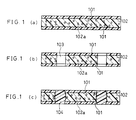
- An electric connecting member for the connection of circuit substrates, said electric connecting member comprising an organic porous base material (102) provided with tackfree films (101) on both sides, and having through-holes (103) through said organic porous base material (102), which are filled with conductive resin compound (104), wherein the conductive resin compound is filled up to the surface of said tackfree films, and the thickness of the tackfree films is such that, upon separation of the tackfree films, the conductive resin compound sticks out on both sides from the outer surface of said organic porous base material (102) in order to improve electrical connection between the circuit substrates.
- A method of manufacturing an electric connecting member for the connection of circuit substrates, said method comprising the steps of:(a) providing an organic porous base material (102) with tackfree films (101) on both sides, said organic porous base material (102) having through-holes (103), and said through-holes being filled with conductive resin compound (104) up to the surface of said tackfree films,(b) separating said tackfree films from said connecting member such that the conductive resin compound (104) sticks out from the surface of the organic porous base material (102).
- A method of manufacturing a multilayer circuit substrate comprising the steps of:(a) providing a multilayer circuit substrate (305) having at least two layers of circuit patterns (306), a circuit substrate (305) having at least one layer of circuit pattern (306), and an electric connecting member (309) for said substrates (305), said electric connecting member (309) comprising an organic porous base material (302) and through-holes through said organic porous base material (102), said through-holes being filled with conductive resin compound (304) that sticks out on both sides from the outer surface of said organic porous base material (302),(b) positioning said connecting member (309) between the multilayer circuit substrate (305) and the circuit substrate (305), and(c) heating and pressurizing.
- A method of manufacturing a multilayer circuit substrate comprising the steps of:(a) providing a multilayer circuit substrate (410) having at least two layers of circuit patterns (413) and two electric connecting members (414, 415), each of said electric connecting members (414, 415) comprising an organic porous base material and through-holes through said organic porous base material, said through-holes being filled with conductive resin compound (418) that sticks out on both sides from the outer surface of said organic porous base material.(b) positioning said multilayer circuit substrate (410) between the two electric connecting members (414, 415);(c) applying a metal foil on both sides; and(d) heating and pressurizing, and forming circuit patterns on said metal foils.
- The electric connecting member and the method according to any of claims 1 to 4, wherein said organic porous base material is a composite material which comprises a nonwoven heat-resisting synthetic fiber fabric impregnated with an uncured thermosetting resin.
- The electric connecting member and the method according to claim 5, wherein said nonwoven heat-resisting synthetic fiber fabric comprises aramid resin, and said uncured thermosetting resin is epoxy resin.
- The electric connecting member and the method according to claim 5, wherein said nonwoven heat-resisting synthetic fiber fabric comprises paper, and said uncured thermosetting resin is selected from the group consisting of phenol resin and epoxy resin.
- The electric connecting member and the method according to any of claims 1 to 7, wherein a conductive substance contained in said conductive resin compound is at least one metallic powder selected from the group consisting of silver, nickel, copper, silver alloy, nickel alloy, and copper alloy.
- The electric connecting member and the method according to any of claims 1 to 8, wherein a resin component contained in said conductive resin compound is the same as the thermosetting resin in said organic porous base material.
- The method of manufacturing a multilayer circuit substrate according to claim 3 or 4, wherein said multilayer circuit substrate having at least two layers of circuit patterns and/or said circuit substrate having at least one layer of circuit pattern comprise glass-epoxy substrates having copper foil wirings and copper-plated through-holes.
- The method of manufacturing a multilayer circuit substrate according to claim 3 or 4, wherein said multilayer circuit substrate having at least two layers of circuit patterns and/or said circuit substrate having at least one layer of circuit pattern comprise aramid nonwoven fabrics and thermosetting epoxy resin.
- The electric connecting member and the method according to any of claims 1 to 11, wherein said through-holes are formed by laser irradiation.
- The electric connecting member and the method according to any of claims 1 to 12, wherein said through-holes filled with the conductive resin compound have a diameter of 50 µm to 1 mm.
- The electric connecting member and the method according to any of claims 1 to 13, wherein said through-holes filled with the conductive resin compound have a pitch of 50 µm or more.
- The electric connecting member and the method according to any of claims 1 to 14, wherein said through-holes filled with the conductive resin compound have an electrical resistance of 0.05 to 5.0mΩ.
- The electric connecting member and the method according to any of claims 1 to 15, wherein said porous base material has a porosity of from 2 to 35%.
- The method of manufacturing a multilayer circuit substrate according to claim 3 or 4, wherein the heating is carried out at a temperature of from 170 to 260 °C.
- The method of manufacturing a multilayer circuit substrate according to claim 3 or 4, wherein the pressurization is carried out at a pressure of from 20 to 80 kg/cm2.
Applications Claiming Priority (4)
| Application Number | Priority Date | Filing Date | Title |
|---|---|---|---|
| JP23451993 | 1993-09-21 | ||
| JP234519/93 | 1993-09-21 | ||
| JP242450/93 | 1993-09-29 | ||
| JP24245093 | 1993-09-29 |
Publications (2)
| Publication Number | Publication Date |
|---|---|
| EP0645950A1 EP0645950A1 (en) | 1995-03-29 |
| EP0645950B1 true EP0645950B1 (en) | 1998-09-02 |
Family
ID=26531606
Family Applications (1)
| Application Number | Title | Priority Date | Filing Date |
|---|---|---|---|
| EP19940114796 Expired - Lifetime EP0645950B1 (en) | 1993-09-21 | 1994-09-20 | Connecting member of a circuit substrate and method of manufacturing multilayer circuit substrates by using the same |
Country Status (4)
| Country | Link |
|---|---|
| US (3) | US5484647A (en) |
| EP (1) | EP0645950B1 (en) |
| CN (1) | CN1075338C (en) |
| DE (1) | DE69412952T2 (en) |
Cited By (2)
| Publication number | Priority date | Publication date | Assignee | Title |
|---|---|---|---|---|
| DE102004045451A1 (en) * | 2004-09-20 | 2006-03-30 | Atotech Deutschland Gmbh | Galvanic process for filling through-holes with metals, in particular printed circuit boards with copper |
| US8784634B2 (en) | 2006-03-30 | 2014-07-22 | Atotech Deutschland Gmbh | Electrolytic method for filling holes and cavities with metals |
Families Citing this family (162)
| Publication number | Priority date | Publication date | Assignee | Title |
|---|---|---|---|---|
| JP2756075B2 (en) * | 1993-08-06 | 1998-05-25 | 三菱電機株式会社 | Metal base substrate and electronic device using the same |
| JPH08148240A (en) * | 1994-09-20 | 1996-06-07 | Whitaker Corp:The | Connector |
| FR2726397B1 (en) * | 1994-10-28 | 1996-11-22 | Commissariat Energie Atomique | ANISOTROPIC CONDUCTIVE FILM FOR MICROCONNECTICS |
| JP3311899B2 (en) * | 1995-01-20 | 2002-08-05 | 松下電器産業株式会社 | Circuit board and method of manufacturing the same |
| US5837356A (en) * | 1995-09-22 | 1998-11-17 | Kyocera Corporation | Wiring board and method for manufacturing the same |
| EP0774888B1 (en) | 1995-11-16 | 2003-03-19 | Matsushita Electric Industrial Co., Ltd | Printed wiring board and assembly of the same |
| JP3241605B2 (en) | 1996-09-06 | 2001-12-25 | 松下電器産業株式会社 | Wiring board manufacturing method and wiring board |
| US6703565B1 (en) | 1996-09-06 | 2004-03-09 | Matsushita Electric Industrial Co., Ltd. | Printed wiring board |
| JP3889856B2 (en) | 1997-06-30 | 2007-03-07 | 松下電器産業株式会社 | Method for manufacturing printed wiring board with protruding electrodes |
| TW410534B (en) * | 1997-07-16 | 2000-11-01 | Matsushita Electric Ind Co Ltd | Wiring board and production process for the same |
| US5902438A (en) * | 1997-08-13 | 1999-05-11 | Fry's Metals, Inc. | Process for the formation of anisotropic conducting material |
| US6376049B1 (en) * | 1997-10-14 | 2002-04-23 | Ibiden Co., Ltd. | Multilayer printed wiring board and its manufacturing method, and resin composition for filling through-hole |
| JP2974007B1 (en) * | 1997-10-20 | 1999-11-08 | 新神戸電機株式会社 | Polishing object holding material and method of manufacturing polishing object |
| US6038133A (en) * | 1997-11-25 | 2000-03-14 | Matsushita Electric Industrial Co., Ltd. | Circuit component built-in module and method for producing the same |
| US6620731B1 (en) * | 1997-12-18 | 2003-09-16 | Micron Technology, Inc. | Method for fabricating semiconductor components and interconnects with contacts on opposing sides |
| US6833613B1 (en) * | 1997-12-18 | 2004-12-21 | Micron Technology, Inc. | Stacked semiconductor package having laser machined contacts |
| US6406939B1 (en) | 1998-05-02 | 2002-06-18 | Charles W. C. Lin | Flip chip assembly with via interconnection |
| SG75841A1 (en) | 1998-05-02 | 2000-10-24 | Eriston Invest Pte Ltd | Flip chip assembly with via interconnection |
| SG86345A1 (en) | 1998-05-14 | 2002-02-19 | Matsushita Electric Ind Co Ltd | Circuit board and method of manufacturing the same |
| US6565954B2 (en) | 1998-05-14 | 2003-05-20 | Matsushita Electric Industrial Co., Ltd. | Circuit board and method of manufacturing the same |
| TWI228610B (en) * | 1998-07-31 | 2005-03-01 | Toshiba Corp | Flat panel display unit |
| ATE333207T1 (en) | 1998-11-09 | 2006-08-15 | Ballard Power Systems | ELECTRICAL CONTACT DEVICE FOR A FUEL CELL |
| SG82590A1 (en) | 1998-12-17 | 2001-08-21 | Eriston Technologies Pte Ltd | Bumpless flip chip assembly with strips and via-fill |
| TW522536B (en) | 1998-12-17 | 2003-03-01 | Wen-Chiang Lin | Bumpless flip chip assembly with strips-in-via and plating |
| SG82591A1 (en) | 1998-12-17 | 2001-08-21 | Eriston Technologies Pte Ltd | Bumpless flip chip assembly with solder via |
| JP2001007469A (en) * | 1999-06-23 | 2001-01-12 | Sony Corp | Printed circuit board and its manufacture |
| US6245696B1 (en) | 1999-06-25 | 2001-06-12 | Honeywell International Inc. | Lasable bond-ply materials for high density printed wiring boards |
| US6224965B1 (en) | 1999-06-25 | 2001-05-01 | Honeywell International Inc. | Microfiber dielectrics which facilitate laser via drilling |
| US7538237B2 (en) * | 1999-07-02 | 2009-05-26 | Kreido Laboratories | Process for high shear gas-liquid reactions |
| US6471392B1 (en) | 2001-03-07 | 2002-10-29 | Holl Technologies Company | Methods and apparatus for materials processing |
| US6742774B2 (en) * | 1999-07-02 | 2004-06-01 | Holl Technologies Company | Process for high shear gas-liquid reactions |
| JP2001053438A (en) * | 1999-08-16 | 2001-02-23 | Sony Corp | Method for manufacturing multi-layer printed wiring board |
| US6319829B1 (en) | 1999-08-18 | 2001-11-20 | International Business Machines Corporation | Enhanced interconnection to ceramic substrates |
| JP4345153B2 (en) | 1999-09-27 | 2009-10-14 | ソニー株式会社 | Manufacturing method of video display device |
| WO2001045478A1 (en) * | 1999-12-14 | 2001-06-21 | Matsushita Electric Industrial Co. Ltd. | Multilayered printed wiring board and production method therefor |
| US6871396B2 (en) | 2000-02-09 | 2005-03-29 | Matsushita Electric Industrial Co., Ltd. | Transfer material for wiring substrate |
| TW569424B (en) | 2000-03-17 | 2004-01-01 | Matsushita Electric Ind Co Ltd | Module with embedded electric elements and the manufacturing method thereof |
| TWI242398B (en) * | 2000-06-14 | 2005-10-21 | Matsushita Electric Ind Co Ltd | Printed circuit board and method of manufacturing the same |
| US6518514B2 (en) * | 2000-08-21 | 2003-02-11 | Matsushita Electric Industrial Co., Ltd. | Circuit board and production of the same |
| US6402970B1 (en) | 2000-08-22 | 2002-06-11 | Charles W. C. Lin | Method of making a support circuit for a semiconductor chip assembly |
| US6660626B1 (en) | 2000-08-22 | 2003-12-09 | Charles W. C. Lin | Semiconductor chip assembly with simultaneously electrolessly plated contact terminal and connection joint |
| US6403460B1 (en) | 2000-08-22 | 2002-06-11 | Charles W. C. Lin | Method of making a semiconductor chip assembly |
| US6350633B1 (en) | 2000-08-22 | 2002-02-26 | Charles W. C. Lin | Semiconductor chip assembly with simultaneously electroplated contact terminal and connection joint |
| US6551861B1 (en) | 2000-08-22 | 2003-04-22 | Charles W. C. Lin | Method of making a semiconductor chip assembly by joining the chip to a support circuit with an adhesive |
| US6562657B1 (en) | 2000-08-22 | 2003-05-13 | Charles W. C. Lin | Semiconductor chip assembly with simultaneously electrolessly plated contact terminal and connection joint |
| US6562709B1 (en) | 2000-08-22 | 2003-05-13 | Charles W. C. Lin | Semiconductor chip assembly with simultaneously electroplated contact terminal and connection joint |
| US6436734B1 (en) | 2000-08-22 | 2002-08-20 | Charles W. C. Lin | Method of making a support circuit for a semiconductor chip assembly |
| JP2002094200A (en) * | 2000-09-18 | 2002-03-29 | Matsushita Electric Ind Co Ltd | Circuit board, electric insulating material therefor and method of manufacturing the same |
| US6350632B1 (en) | 2000-09-20 | 2002-02-26 | Charles W. C. Lin | Semiconductor chip assembly with ball bond connection joint |
| US6511865B1 (en) | 2000-09-20 | 2003-01-28 | Charles W. C. Lin | Method for forming a ball bond connection joint on a conductive trace and conductive pad in a semiconductor chip assembly |
| US6350386B1 (en) | 2000-09-20 | 2002-02-26 | Charles W. C. Lin | Method of making a support circuit with a tapered through-hole for a semiconductor chip assembly |
| EP1194020A3 (en) * | 2000-09-27 | 2004-03-31 | Matsushita Electric Industrial Co., Ltd. | Resin board, manufacturing process for resin board, connection medium body, circuit board and manufacturing process for circuit board |
| US6448108B1 (en) | 2000-10-02 | 2002-09-10 | Charles W. C. Lin | Method of making a semiconductor chip assembly with a conductive trace subtractively formed before and after chip attachment |
| US6544813B1 (en) | 2000-10-02 | 2003-04-08 | Charles W. C. Lin | Method of making a semiconductor chip assembly with a conductive trace subtractively formed before and after chip attachment |
| US7414319B2 (en) * | 2000-10-13 | 2008-08-19 | Bridge Semiconductor Corporation | Semiconductor chip assembly with metal containment wall and solder terminal |
| US7262082B1 (en) | 2000-10-13 | 2007-08-28 | Bridge Semiconductor Corporation | Method of making a three-dimensional stacked semiconductor package with a metal pillar and a conductive interconnect in an encapsulant aperture |
| US6673710B1 (en) | 2000-10-13 | 2004-01-06 | Bridge Semiconductor Corporation | Method of connecting a conductive trace and an insulative base to a semiconductor chip |
| US6667229B1 (en) | 2000-10-13 | 2003-12-23 | Bridge Semiconductor Corporation | Method of connecting a bumped compliant conductive trace and an insulative base to a semiconductor chip |
| US7129575B1 (en) | 2000-10-13 | 2006-10-31 | Bridge Semiconductor Corporation | Semiconductor chip assembly with bumped metal pillar |
| US6492252B1 (en) | 2000-10-13 | 2002-12-10 | Bridge Semiconductor Corporation | Method of connecting a bumped conductive trace to a semiconductor chip |
| US7264991B1 (en) | 2000-10-13 | 2007-09-04 | Bridge Semiconductor Corporation | Method of connecting a conductive trace to a semiconductor chip using conductive adhesive |
| US6740576B1 (en) | 2000-10-13 | 2004-05-25 | Bridge Semiconductor Corporation | Method of making a contact terminal with a plated metal peripheral sidewall portion for a semiconductor chip assembly |
| US7094676B1 (en) | 2000-10-13 | 2006-08-22 | Bridge Semiconductor Corporation | Semiconductor chip assembly with embedded metal pillar |
| US6872591B1 (en) | 2000-10-13 | 2005-03-29 | Bridge Semiconductor Corporation | Method of making a semiconductor chip assembly with a conductive trace and a substrate |
| US6699780B1 (en) | 2000-10-13 | 2004-03-02 | Bridge Semiconductor Corporation | Method of connecting a conductive trace to a semiconductor chip using plasma undercut etching |
| US6984576B1 (en) | 2000-10-13 | 2006-01-10 | Bridge Semiconductor Corporation | Method of connecting an additively and subtractively formed conductive trace and an insulative base to a semiconductor chip |
| US7132741B1 (en) | 2000-10-13 | 2006-11-07 | Bridge Semiconductor Corporation | Semiconductor chip assembly with carved bumped terminal |
| US7075186B1 (en) | 2000-10-13 | 2006-07-11 | Bridge Semiconductor Corporation | Semiconductor chip assembly with interlocked contact terminal |
| US6576539B1 (en) | 2000-10-13 | 2003-06-10 | Charles W.C. Lin | Semiconductor chip assembly with interlocked conductive trace |
| US7129113B1 (en) | 2000-10-13 | 2006-10-31 | Bridge Semiconductor Corporation | Method of making a three-dimensional stacked semiconductor package with a metal pillar in an encapsulant aperture |
| US6949408B1 (en) | 2000-10-13 | 2005-09-27 | Bridge Semiconductor Corporation | Method of connecting a conductive trace and an insulative base to a semiconductor chip using multiple etch steps |
| US6440835B1 (en) | 2000-10-13 | 2002-08-27 | Charles W. C. Lin | Method of connecting a conductive trace to a semiconductor chip |
| US7190080B1 (en) | 2000-10-13 | 2007-03-13 | Bridge Semiconductor Corporation | Semiconductor chip assembly with embedded metal pillar |
| US6576493B1 (en) | 2000-10-13 | 2003-06-10 | Bridge Semiconductor Corporation | Method of connecting a conductive trace and an insulative base to a semiconductor chip using multiple etch steps |
| US7071089B1 (en) | 2000-10-13 | 2006-07-04 | Bridge Semiconductor Corporation | Method of making a semiconductor chip assembly with a carved bumped terminal |
| US7319265B1 (en) | 2000-10-13 | 2008-01-15 | Bridge Semiconductor Corporation | Semiconductor chip assembly with precision-formed metal pillar |
| US6537851B1 (en) | 2000-10-13 | 2003-03-25 | Bridge Semiconductor Corporation | Method of connecting a bumped compliant conductive trace to a semiconductor chip |
| US6908788B1 (en) | 2000-10-13 | 2005-06-21 | Bridge Semiconductor Corporation | Method of connecting a conductive trace to a semiconductor chip using a metal base |
| US6548393B1 (en) | 2000-10-13 | 2003-04-15 | Charles W. C. Lin | Semiconductor chip assembly with hardened connection joint |
| US7009297B1 (en) | 2000-10-13 | 2006-03-07 | Bridge Semiconductor Corporation | Semiconductor chip assembly with embedded metal particle |
| US6876072B1 (en) | 2000-10-13 | 2005-04-05 | Bridge Semiconductor Corporation | Semiconductor chip assembly with chip in substrate cavity |
| US6444489B1 (en) | 2000-12-15 | 2002-09-03 | Charles W. C. Lin | Semiconductor chip assembly with bumped molded substrate |
| TW511405B (en) * | 2000-12-27 | 2002-11-21 | Matsushita Electric Ind Co Ltd | Device built-in module and manufacturing method thereof |
| JP3760771B2 (en) * | 2001-01-16 | 2006-03-29 | 松下電器産業株式会社 | Circuit forming substrate and method of manufacturing circuit forming substrate |
| JP2002232135A (en) * | 2001-01-30 | 2002-08-16 | Matsushita Electric Ind Co Ltd | Double-sided circuit board for lamination and its manufacturing method, and multilayer printed circuit board using the same |
| US6653170B1 (en) | 2001-02-06 | 2003-11-25 | Charles W. C. Lin | Semiconductor chip assembly with elongated wire ball bonded to chip and electrolessly plated to support circuit |
| JP2002293979A (en) | 2001-03-30 | 2002-10-09 | Sumitomo Chem Co Ltd | Porous para-oriented aromatic polyamide film, its prepreg and substrate using prepreg and used for printed circuit |
| US20040170795A1 (en) * | 2001-04-04 | 2004-09-02 | Alliedsignal Inc. | Lasable bond-ply materials for high density printed wiring boards |
| US6830806B2 (en) * | 2001-04-12 | 2004-12-14 | Kreido Laboratories | Methods of manufacture of electric circuit substrates and components having multiple electric characteristics and substrates and components so manufactured |
| JP2002353032A (en) * | 2001-05-18 | 2002-12-06 | Rotra Leiterplatten Produktions & Vertriebs Gmbh | Multilayer build-up printed board and its producing method |
| US6768064B2 (en) * | 2001-07-10 | 2004-07-27 | Fujikura Ltd. | Multilayer wiring board assembly, multilayer wiring board assembly component and method of manufacture thereof |
| EP1408724A4 (en) * | 2001-07-18 | 2007-05-23 | Matsushita Electric Ind Co Ltd | Circuit formed substrate and method of manufacturing circuit formed substrate |
| TW558931B (en) * | 2001-07-18 | 2003-10-21 | Matsushita Electric Ind Co Ltd | Manufacturing method of printed wiring boards and material for manufacturing printed wiring boards |
| US20040185237A1 (en) * | 2001-08-07 | 2004-09-23 | Kohichiro Kawate | Sheet for sealing electrical wiring |
| US6908318B2 (en) * | 2001-08-08 | 2005-06-21 | 3M Innovative Properties Company | Batch electrically connecting sheet |
| US20030066624A1 (en) * | 2001-09-13 | 2003-04-10 | Holl Richard A. | Methods and apparatus for transfer of heat energy between a body surface and heat transfer fluid |
| US6500529B1 (en) * | 2001-09-14 | 2002-12-31 | Tonoga, Ltd. | Low signal loss bonding ply for multilayer circuit boards |
| US6787246B2 (en) | 2001-10-05 | 2004-09-07 | Kreido Laboratories | Manufacture of flat surfaced composites comprising powdered fillers in a polymer matrix |
| US6826830B2 (en) * | 2002-02-05 | 2004-12-07 | International Business Machines Corporation | Multi-layered interconnect structure using liquid crystalline polymer dielectric |
| US7049528B2 (en) * | 2002-02-06 | 2006-05-23 | Ibiden Co., Ltd. | Semiconductor chip mounting wiring board, manufacturing method for same, and semiconductor module |
| JP2004031555A (en) * | 2002-06-25 | 2004-01-29 | Nec Corp | Circuit board device and connection method between substrates |
| US7438969B2 (en) * | 2002-07-10 | 2008-10-21 | Ngk Spark Plug Co., Ltd. | Filling material, multilayer wiring board, and process of producing multilayer wiring board |
| US7098360B2 (en) * | 2002-07-16 | 2006-08-29 | Kreido Laboratories | Processes employing multiple successive chemical reaction process steps and apparatus therefore |
| US7165881B2 (en) * | 2002-09-11 | 2007-01-23 | Holl Technologies Corporation | Methods and apparatus for high-shear mixing and reacting of materials |
| WO2004030802A2 (en) * | 2002-10-03 | 2004-04-15 | Kreido Laboratories | Apparatus for transfer of heat energy between a body surface and heat transfer fluid |
| US6603201B1 (en) * | 2002-10-23 | 2003-08-05 | Lsi Logic Corporation | Electronic substrate |
| WO2004060656A1 (en) * | 2003-01-06 | 2004-07-22 | Toray Industries, Inc. | Laminated film and method for producing same |
| US7394663B2 (en) * | 2003-02-18 | 2008-07-01 | Matsushita Electric Industrial Co., Ltd. | Electronic component built-in module and method of manufacturing the same |
| JP2004319530A (en) * | 2003-02-28 | 2004-11-11 | Sanyo Electric Co Ltd | Optical semiconductor device and its manufacturing process |
| KR100570856B1 (en) * | 2003-04-02 | 2006-04-12 | 삼성전기주식회사 | Method for fabricating the multi layer PCB in parallel |
| US7141874B2 (en) * | 2003-05-14 | 2006-11-28 | Matsushita Electric Industrial Co., Ltd. | Electronic component packaging structure and method for producing the same |
| US20050016762A1 (en) * | 2003-07-22 | 2005-01-27 | Unitech Printed Circuit Board Corp. | Method of forming a multi-layer printed circuit board and the product thereof |
| JP2005045150A (en) * | 2003-07-25 | 2005-02-17 | Matsushita Electric Ind Co Ltd | Wiring base material for intermediate connection, multilayer wiring board, and manufacturing methods thereof |
| ATE419661T1 (en) * | 2003-09-09 | 2009-01-15 | Nitto Denko Corp | ANISOTROPIC CONDUCTING FILM, PROCESS OF PRODUCTION AND USE |
| US7993983B1 (en) | 2003-11-17 | 2011-08-09 | Bridge Semiconductor Corporation | Method of making a semiconductor chip assembly with chip and encapsulant grinding |
| US7425759B1 (en) | 2003-11-20 | 2008-09-16 | Bridge Semiconductor Corporation | Semiconductor chip assembly with bumped terminal and filler |
| US7538415B1 (en) | 2003-11-20 | 2009-05-26 | Bridge Semiconductor Corporation | Semiconductor chip assembly with bumped terminal, filler and insulative base |
| JP2005340687A (en) * | 2004-05-31 | 2005-12-08 | Fujitsu Ltd | Laminated substrate and its manufacturing method, and electronic apparatus having such laminated substrate |
| JP4416616B2 (en) * | 2004-09-29 | 2010-02-17 | 株式会社リコー | Electronic component mounting body and electronic equipment |
| US7750483B1 (en) | 2004-11-10 | 2010-07-06 | Bridge Semiconductor Corporation | Semiconductor chip assembly with welded metal pillar and enlarged plated contact terminal |
| US7268421B1 (en) | 2004-11-10 | 2007-09-11 | Bridge Semiconductor Corporation | Semiconductor chip assembly with welded metal pillar that includes enlarged ball bond |
| US7786567B2 (en) * | 2004-11-10 | 2010-08-31 | Chung-Cheng Wang | Substrate for electrical device and methods for making the same |
| US7446419B1 (en) | 2004-11-10 | 2008-11-04 | Bridge Semiconductor Corporation | Semiconductor chip assembly with welded metal pillar of stacked metal balls |
| WO2006080073A1 (en) * | 2005-01-27 | 2006-08-03 | Matsushita Electric Industrial Co., Ltd. | Multi-layer circuit substrate manufacturing method and multi-layer circuit substrate |
| US7286366B2 (en) * | 2005-03-24 | 2007-10-23 | Motorola, Inc. | Multilayer circuit board with embedded components and method of manufacture |
| JP2007005246A (en) * | 2005-06-27 | 2007-01-11 | Sumitomo Electric Ind Ltd | Porous resin base material and multilayer substrate |
| JP2007012810A (en) * | 2005-06-29 | 2007-01-18 | Renesas Technology Corp | Method of manufacturing semiconductor integrated circuit device |
| JP4689375B2 (en) * | 2005-07-07 | 2011-05-25 | 富士通株式会社 | Laminated substrate and electronic device having the laminated substrate |
| US7759582B2 (en) * | 2005-07-07 | 2010-07-20 | Ibiden Co., Ltd. | Multilayer printed wiring board |
| US7834273B2 (en) | 2005-07-07 | 2010-11-16 | Ibiden Co., Ltd. | Multilayer printed wiring board |
| TW200706743A (en) * | 2005-07-29 | 2007-02-16 | Nichiha Co Ltd | Stain-proofing agent and building board using the same |
| US7811863B1 (en) | 2006-10-26 | 2010-10-12 | Bridge Semiconductor Corporation | Method of making a semiconductor chip assembly with metal pillar and encapsulant grinding and heat sink attachment |
| US7494843B1 (en) | 2006-12-26 | 2009-02-24 | Bridge Semiconductor Corporation | Method of making a semiconductor chip assembly with thermal conductor and encapsulant grinding |
| FR2908955A1 (en) * | 2006-11-17 | 2008-05-23 | Novatec Sa | Electronic circuits interconnecting element i.e. keyboard, has conducting material placed in hole of insulating sheet and forming protuberances on both sides of hole, where protuberances have diameter larger than that of hole |
| US7851342B2 (en) * | 2007-03-30 | 2010-12-14 | Intel Corporation | In-situ formation of conductive filling material in through-silicon via |
| TW200906263A (en) * | 2007-05-29 | 2009-02-01 | Matsushita Electric Ind Co Ltd | Circuit board and method for manufacturing the same |
| JP5272655B2 (en) * | 2008-10-31 | 2013-08-28 | パナソニック株式会社 | Molded motor |
| JP2011029488A (en) * | 2009-07-28 | 2011-02-10 | Kyocera Corp | Wiring board |
| US8383948B2 (en) * | 2009-09-18 | 2013-02-26 | Ibiden Co., Ltd. | Flex-rigid wiring board and method for manufacturing the same |
| US8933556B2 (en) * | 2010-01-22 | 2015-01-13 | Ibiden Co., Ltd. | Wiring board |
| JP4859999B1 (en) * | 2010-12-21 | 2012-01-25 | パナソニック株式会社 | Multilayer wiring substrate, multilayer wiring substrate manufacturing method, and via paste |
| JP4917668B1 (en) * | 2010-12-29 | 2012-04-18 | パナソニック株式会社 | Multilayer wiring board and method for manufacturing multilayer wiring board |
| US9279051B2 (en) * | 2011-09-22 | 2016-03-08 | Elite Material Co., Ltd. | Halogen-free resin composition, and copper clad laminate and printed circuit board using same |
| CN104409364B (en) * | 2014-11-19 | 2017-12-01 | 清华大学 | Pinboard and preparation method thereof, encapsulating structure and the bonding method for pinboard |
| US9666514B2 (en) * | 2015-04-14 | 2017-05-30 | Invensas Corporation | High performance compliant substrate |
| KR102340938B1 (en) * | 2015-09-17 | 2021-12-20 | 엘지디스플레이 주식회사 | Display device and method of measuring contact resistance thereof |
| CN106231819B (en) * | 2016-08-18 | 2019-07-19 | 武汉华尚绿能科技股份有限公司 | A kind of preparation method of transparent glass base double-layer circuit board |
| CN106304623B (en) * | 2016-08-18 | 2018-04-17 | 武汉华尚绿能科技股份有限公司 | A kind of transparent glass base double-layer circuit board |
| JP6810617B2 (en) * | 2017-01-16 | 2021-01-06 | 富士通インターコネクトテクノロジーズ株式会社 | Circuit boards, circuit board manufacturing methods and electronic devices |
| CN106848761B (en) * | 2017-01-20 | 2019-02-01 | 深圳市新升华电子器件有限公司 | USB Type-C connector |
| US10440828B2 (en) * | 2017-04-14 | 2019-10-08 | The Diller Corporation | Integrated electrical component within laminate |
| CN109429420B (en) * | 2017-08-22 | 2021-11-16 | 宏启胜精密电子(秦皇岛)有限公司 | Circuit board with electromagnetic shielding function and manufacturing method thereof |
| CN110322985A (en) * | 2018-03-28 | 2019-10-11 | 上海逻骅投资管理合伙企业(有限合伙) | A kind of electrocondution slurry and its preparation method and application |
| CN110324963A (en) * | 2018-03-28 | 2019-10-11 | 上海逻骅投资管理合伙企业(有限合伙) | Electrocondution slurry and its preparation method and application |
| US11224131B2 (en) * | 2018-04-04 | 2022-01-11 | Lenovo (Singapore) Pte. Ltd. | Systems and methods for surface mounting cable connections |
| CN110366329A (en) * | 2018-04-10 | 2019-10-22 | 电连技术股份有限公司 | A kind of manufacturing method and multilager base plate of multilager base plate |
| CN108535928A (en) * | 2018-04-13 | 2018-09-14 | 京东方科技集团股份有限公司 | A kind of array substrate and preparation method thereof, display panel and display device |
| CN109121284A (en) * | 2018-09-05 | 2019-01-01 | 深圳市华讯方舟太赫兹科技有限公司 | Single pole multiple throw circuit board applied to millimeter wave rays safety detection apparatus |
| CN111312680B (en) * | 2018-12-12 | 2022-10-28 | 深南电路股份有限公司 | Bearing plate of coreless packaging substrate and preparation method |
| EP3709779A1 (en) * | 2019-03-12 | 2020-09-16 | AT & S Austria Technologie & Systemtechnik Aktiengesellschaft | Component carrier and method of manufacturing the same |
| CN111757593B (en) * | 2020-06-29 | 2023-12-22 | 深圳市百柔新材料技术有限公司 | Glass core board and preparation method thereof |
| CN115250565A (en) * | 2021-04-27 | 2022-10-28 | 华为技术有限公司 | Circuit board assembly and electronic equipment |
Family Cites Families (11)
| Publication number | Priority date | Publication date | Assignee | Title |
|---|---|---|---|---|
| JPS5278069A (en) * | 1975-12-24 | 1977-07-01 | Fuji Kinzoku Kakou Kk | Printed circuit board |
| US4383363A (en) * | 1977-09-01 | 1983-05-17 | Sharp Kabushiki Kaisha | Method of making a through-hole connector |
| US4657778A (en) * | 1984-08-01 | 1987-04-14 | Moran Peter L | Multilayer systems and their method of production |
| JPS6437079A (en) * | 1987-07-31 | 1989-02-07 | Shin Kobe Electric Machinery | Manufacture of through-hole printed wiring board |
| JPH01151293A (en) * | 1987-12-09 | 1989-06-14 | Mari Yamazaki | Method for conducting inner layer of multilayer printed wiring board |
| US4967314A (en) * | 1988-03-28 | 1990-10-30 | Prime Computer Inc. | Circuit board construction |
| JPH03222393A (en) * | 1990-01-26 | 1991-10-01 | Hitachi Chem Co Ltd | Connection of circuits formed on both sides of printing wiring board |
| JPH0567869A (en) * | 1991-09-05 | 1993-03-19 | Matsushita Electric Ind Co Ltd | Method of bonding electric part, module and multilayer board |
| JPH05175649A (en) * | 1991-12-25 | 1993-07-13 | Tokuyama Soda Co Ltd | Manufacture of circuit board |
| JP2601128B2 (en) * | 1992-05-06 | 1997-04-16 | 松下電器産業株式会社 | Method of manufacturing circuit forming substrate and circuit forming substrate |
| US5652042A (en) * | 1993-10-29 | 1997-07-29 | Matsushita Electric Industrial Co., Ltd. | Conductive paste compound for via hole filling, printed circuit board which uses the conductive paste |
-
1994
- 1994-09-20 DE DE1994612952 patent/DE69412952T2/en not_active Expired - Lifetime
- 1994-09-20 US US08/308,982 patent/US5484647A/en not_active Expired - Lifetime
- 1994-09-20 EP EP19940114796 patent/EP0645950B1/en not_active Expired - Lifetime
- 1994-09-20 CN CN94113752A patent/CN1075338C/en not_active Expired - Lifetime
-
1996
- 1996-01-04 US US08/582,930 patent/US6108903A/en not_active Expired - Lifetime
-
2001
- 2001-01-26 US US09/769,260 patent/US20010003610A1/en not_active Abandoned
Cited By (4)
| Publication number | Priority date | Publication date | Assignee | Title |
|---|---|---|---|---|
| DE102004045451A1 (en) * | 2004-09-20 | 2006-03-30 | Atotech Deutschland Gmbh | Galvanic process for filling through-holes with metals, in particular printed circuit boards with copper |
| DE102004045451B4 (en) * | 2004-09-20 | 2007-05-03 | Atotech Deutschland Gmbh | Galvanic process for filling through-holes with metals, in particular printed circuit boards with copper |
| US9445510B2 (en) | 2004-09-20 | 2016-09-13 | Atotech Deutschland Gmbh | Galvanic process for filling through-holes with metals, in particular of printed circuit boards with copper |
| US8784634B2 (en) | 2006-03-30 | 2014-07-22 | Atotech Deutschland Gmbh | Electrolytic method for filling holes and cavities with metals |
Also Published As
| Publication number | Publication date |
|---|---|
| US5484647A (en) | 1996-01-16 |
| CN1108026A (en) | 1995-09-06 |
| EP0645950A1 (en) | 1995-03-29 |
| DE69412952T2 (en) | 1999-05-12 |
| US6108903A (en) | 2000-08-29 |
| DE69412952D1 (en) | 1998-10-08 |
| CN1075338C (en) | 2001-11-21 |
| US20010003610A1 (en) | 2001-06-14 |
Similar Documents
| Publication | Publication Date | Title |
|---|---|---|
| EP0645950B1 (en) | Connecting member of a circuit substrate and method of manufacturing multilayer circuit substrates by using the same | |
| US5888627A (en) | Printed circuit board and method for the manufacture of same | |
| US6459046B1 (en) | Printed circuit board and method for producing the same | |
| JP2587596B2 (en) | Circuit board connecting material and method for manufacturing multilayer circuit board using the same | |
| EP0591761B1 (en) | A two-sided printed circuit board, a multi-layered printed circuit board, and a method for producing the same | |
| US6673190B2 (en) | Lasable bond-ply materials for high density printed wiring boards | |
| US6096411A (en) | Conductive paste composition for via hole filling and printed circuit board using the same | |
| US5428190A (en) | Rigid-flex board with anisotropic interconnect and method of manufacture | |
| EP0645951B1 (en) | Printed circuit board and method of manufacturing the same | |
| US20040040738A1 (en) | Multilayer wiring board | |
| US6599617B2 (en) | Adhesion strength between conductive paste and lands of printed wiring board, and manufacturing method thereof | |
| US20030137815A1 (en) | Printed wiring board and method of manufacturing the same | |
| US7356916B2 (en) | Circuit-formed substrate and method of manufacturing circuit-formed substrate | |
| TW517504B (en) | Circuit board and a method of manufacturing the same | |
| KR101281898B1 (en) | Multilayer printed wiring board and method for producing same | |
| JPH08316598A (en) | Printed wiring board and production thereof | |
| JPH1037054A (en) | Base material for circuit board, prepreg and printed circuit board using the same | |
| JP3440174B2 (en) | Multilayer printed wiring board and method of manufacturing the same | |
| JP3588888B2 (en) | Method for manufacturing multilayer printed wiring board | |
| JP3576297B2 (en) | Electrical inspection jig and manufacturing method thereof | |
| JP3238901B2 (en) | Multilayer printed wiring board and method of manufacturing the same | |
| JP2000252631A (en) | Multilayer printed wiring board and its manufacture | |
| JPH11163527A (en) | Manufacture of multilayer wiring board | |
| JPH11126972A (en) | Multilayered circuit board and its manufacture | |
| Higgins III | Laminate-Based Technologies for Multichip Modules |
Legal Events
| Date | Code | Title | Description |
|---|---|---|---|
| PUAI | Public reference made under article 153(3) epc to a published international application that has entered the european phase |
Free format text: ORIGINAL CODE: 0009012 |
|
| AK | Designated contracting states |
Kind code of ref document: A1 Designated state(s): DE FR GB |
|
| 17P | Request for examination filed |
Effective date: 19950407 |
|
| 17Q | First examination report despatched |
Effective date: 19950823 |
|
| GRAG | Despatch of communication of intention to grant |
Free format text: ORIGINAL CODE: EPIDOS AGRA |
|
| GRAG | Despatch of communication of intention to grant |
Free format text: ORIGINAL CODE: EPIDOS AGRA |
|
| GRAG | Despatch of communication of intention to grant |
Free format text: ORIGINAL CODE: EPIDOS AGRA |
|
| GRAH | Despatch of communication of intention to grant a patent |
Free format text: ORIGINAL CODE: EPIDOS IGRA |
|
| GRAH | Despatch of communication of intention to grant a patent |
Free format text: ORIGINAL CODE: EPIDOS IGRA |
|
| GRAA | (expected) grant |
Free format text: ORIGINAL CODE: 0009210 |
|
| AK | Designated contracting states |
Kind code of ref document: B1 Designated state(s): DE FR GB |
|
| REF | Corresponds to: |
Ref document number: 69412952 Country of ref document: DE Date of ref document: 19981008 |
|
| ET | Fr: translation filed | ||
| PLBE | No opposition filed within time limit |
Free format text: ORIGINAL CODE: 0009261 |
|
| STAA | Information on the status of an ep patent application or granted ep patent |
Free format text: STATUS: NO OPPOSITION FILED WITHIN TIME LIMIT |
|
| 26N | No opposition filed | ||
| REG | Reference to a national code |
Ref country code: GB Ref legal event code: IF02 |
|
| PGFP | Annual fee paid to national office [announced via postgrant information from national office to epo] |
Ref country code: DE Payment date: 20130918 Year of fee payment: 20 |
|
| PGFP | Annual fee paid to national office [announced via postgrant information from national office to epo] |
Ref country code: FR Payment date: 20130910 Year of fee payment: 20 Ref country code: GB Payment date: 20130918 Year of fee payment: 20 |
|
| REG | Reference to a national code |
Ref country code: DE Ref legal event code: R071 Ref document number: 69412952 Country of ref document: DE |
|
| REG | Reference to a national code |
Ref country code: GB Ref legal event code: PE20 Expiry date: 20140919 |
|
| PG25 | Lapsed in a contracting state [announced via postgrant information from national office to epo] |
Ref country code: DE Free format text: LAPSE BECAUSE OF EXPIRATION OF PROTECTION Effective date: 20140923 |
|
| PG25 | Lapsed in a contracting state [announced via postgrant information from national office to epo] |
Ref country code: GB Free format text: LAPSE BECAUSE OF EXPIRATION OF PROTECTION Effective date: 20140919 |