EP0643404B1 - Inductive structures for semiconductor integrated circuits - Google Patents
Inductive structures for semiconductor integrated circuits Download PDFInfo
- Publication number
- EP0643404B1 EP0643404B1 EP94116854A EP94116854A EP0643404B1 EP 0643404 B1 EP0643404 B1 EP 0643404B1 EP 94116854 A EP94116854 A EP 94116854A EP 94116854 A EP94116854 A EP 94116854A EP 0643404 B1 EP0643404 B1 EP 0643404B1
- Authority
- EP
- European Patent Office
- Prior art keywords
- spiral
- substrate
- variable inductance
- inductance element
- electrically insulating
- Prior art date
- Legal status (The legal status is an assumption and is not a legal conclusion. Google has not performed a legal analysis and makes no representation as to the accuracy of the status listed.)
- Expired - Lifetime
Links
- 239000004065 semiconductor Substances 0.000 title claims 3
- 230000001939 inductive effect Effects 0.000 title description 4
- 239000000758 substrate Substances 0.000 claims description 13
- 239000004020 conductor Substances 0.000 claims description 5
- 230000000149 penetrating effect Effects 0.000 claims description 2
- JBRZTFJDHDCESZ-UHFFFAOYSA-N AsGa Chemical compound [As]#[Ga] JBRZTFJDHDCESZ-UHFFFAOYSA-N 0.000 claims 1
- 229910001218 Gallium arsenide Inorganic materials 0.000 claims 1
- GPXJNWSHGFTCBW-UHFFFAOYSA-N Indium phosphide Chemical compound [In]#P GPXJNWSHGFTCBW-UHFFFAOYSA-N 0.000 claims 1
- 230000003247 decreasing effect Effects 0.000 description 3
- 230000001965 increasing effect Effects 0.000 description 3
- 238000010586 diagram Methods 0.000 description 2
- 230000008878 coupling Effects 0.000 description 1
- 238000010168 coupling process Methods 0.000 description 1
- 238000005859 coupling reaction Methods 0.000 description 1
- 230000004048 modification Effects 0.000 description 1
- 238000012986 modification Methods 0.000 description 1
- 238000004804 winding Methods 0.000 description 1
Images

Classifications
-
- H—ELECTRICITY
- H01—ELECTRIC ELEMENTS
- H01L—SEMICONDUCTOR DEVICES NOT COVERED BY CLASS H10
- H01L28/00—Passive two-terminal components without a potential-jump or surface barrier for integrated circuits; Details thereof; Multistep manufacturing processes therefor
- H01L28/10—Inductors
-
- H—ELECTRICITY
- H01—ELECTRIC ELEMENTS
- H01F—MAGNETS; INDUCTANCES; TRANSFORMERS; SELECTION OF MATERIALS FOR THEIR MAGNETIC PROPERTIES
- H01F17/00—Fixed inductances of the signal type
- H01F17/0006—Printed inductances
-
- H—ELECTRICITY
- H01—ELECTRIC ELEMENTS
- H01F—MAGNETS; INDUCTANCES; TRANSFORMERS; SELECTION OF MATERIALS FOR THEIR MAGNETIC PROPERTIES
- H01F17/00—Fixed inductances of the signal type
- H01F17/0006—Printed inductances
- H01F17/0033—Printed inductances with the coil helically wound around a magnetic core
-
- H—ELECTRICITY
- H01—ELECTRIC ELEMENTS
- H01F—MAGNETS; INDUCTANCES; TRANSFORMERS; SELECTION OF MATERIALS FOR THEIR MAGNETIC PROPERTIES
- H01F21/00—Variable inductances or transformers of the signal type
- H01F21/02—Variable inductances or transformers of the signal type continuously variable, e.g. variometers
- H01F21/08—Variable inductances or transformers of the signal type continuously variable, e.g. variometers by varying the permeability of the core, e.g. by varying magnetic bias
-
- H—ELECTRICITY
- H01—ELECTRIC ELEMENTS
- H01F—MAGNETS; INDUCTANCES; TRANSFORMERS; SELECTION OF MATERIALS FOR THEIR MAGNETIC PROPERTIES
- H01F27/00—Details of transformers or inductances, in general
- H01F27/28—Coils; Windings; Conductive connections
- H01F27/2804—Printed windings
-
- H—ELECTRICITY
- H01—ELECTRIC ELEMENTS
- H01L—SEMICONDUCTOR DEVICES NOT COVERED BY CLASS H10
- H01L23/00—Details of semiconductor or other solid state devices
- H01L23/58—Structural electrical arrangements for semiconductor devices not otherwise provided for, e.g. in combination with batteries
- H01L23/64—Impedance arrangements
- H01L23/645—Inductive arrangements
-
- H—ELECTRICITY
- H01—ELECTRIC ELEMENTS
- H01F—MAGNETS; INDUCTANCES; TRANSFORMERS; SELECTION OF MATERIALS FOR THEIR MAGNETIC PROPERTIES
- H01F17/00—Fixed inductances of the signal type
- H01F17/0006—Printed inductances
- H01F2017/004—Printed inductances with the coil helically wound around an axis without a core
-
- H—ELECTRICITY
- H01—ELECTRIC ELEMENTS
- H01F—MAGNETS; INDUCTANCES; TRANSFORMERS; SELECTION OF MATERIALS FOR THEIR MAGNETIC PROPERTIES
- H01F17/00—Fixed inductances of the signal type
- H01F17/0006—Printed inductances
- H01F2017/0046—Printed inductances with a conductive path having a bridge
-
- H—ELECTRICITY
- H01—ELECTRIC ELEMENTS
- H01F—MAGNETS; INDUCTANCES; TRANSFORMERS; SELECTION OF MATERIALS FOR THEIR MAGNETIC PROPERTIES
- H01F17/00—Fixed inductances of the signal type
- H01F17/0006—Printed inductances
- H01F2017/0086—Printed inductances on semiconductor substrate
-
- H—ELECTRICITY
- H01—ELECTRIC ELEMENTS
- H01L—SEMICONDUCTOR DEVICES NOT COVERED BY CLASS H10
- H01L2924/00—Indexing scheme for arrangements or methods for connecting or disconnecting semiconductor or solid-state bodies as covered by H01L24/00
- H01L2924/0001—Technical content checked by a classifier
- H01L2924/0002—Not covered by any one of groups H01L24/00, H01L24/00 and H01L2224/00
-
- H—ELECTRICITY
- H01—ELECTRIC ELEMENTS
- H01L—SEMICONDUCTOR DEVICES NOT COVERED BY CLASS H10
- H01L2924/00—Indexing scheme for arrangements or methods for connecting or disconnecting semiconductor or solid-state bodies as covered by H01L24/00
- H01L2924/30—Technical effects
- H01L2924/301—Electrical effects
- H01L2924/3011—Impedance
Definitions
- the invention relates to a variable inductance element as claimed in the preamble of claim 1.
- Such kind of element is already known from WO-A-87 07074 comprising: an electrically insulating substrate having opposed first and second surfaces; an electrical conductor disposed in a first spiral on the first surface of the substrate; an electrically insulating film disposed on the first surface and the first spiral; a second electrical conductor disposed in a second spiral on the electrically insulating film and inductively coupled to the first spiral; and means for producing and controlling an electrical current flow through one of said spirals.
- a solution of this object is characterized by: an electrically conducting first via penetrating the electrically insulating film electrically connecting a first end of the first spiral to a first end of the second spiral; and an electrically conducting ground plane disposed on the second surface of the substrate and a second electrically conducting via passing through the substrate from the first to the second surface electrically connecting a second end of the first spiral to the ground plane.
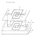
- FIG. 1(a) a perspective view of a variable inductance according to the invention is shown.
- the variable inductance includes two similar spiral inductive structures.
- a spiral 2 includes an electrical conductor disposed on an electrically insulating substrate and a lead 6 in an air bridge structure connecting the internal end 4 of the spiral 2 to a terminal 7.
- the external end 3 of the spiral 2 is directly connected to a terminal 5.
- a similar spiral 62 is disposed on a substrate 1.
- the two spirals 2 and 62 are separated by an electrically insulating film 61.
- the terminals of spiral 62 are connected to an electrical signal source that causes a current to flow through spiral 62.
- the phase and magnitude of that current flow varies the effective inductance of spiral 2 because of the mutual inductive coupling of the two spirals.
- An electrically conducting ground plane 8 is disposed on the surface of substrate 1 opposite that on which spiral 62 is disposed.
- the effective impedance of the spiral 2, Z 1 is a function of the currents I 1 and I 2 and can be varied by controlling I 2 .
- the effective impedance of spiral 2 can also be increased or decreased depending upon the relative phases of the currents I 1 and I 2 .
- terminal 5 of spiral 2 is connected through a via to the external end of spiral 62.
- a circuit 70 is connected in series with spiral 62 for varying the current flowing through spiral 62.
- Circuit 70 may be both an attenuator and an amplifier for decreasing and increasing the current flow through spiral 62.
- the other end of spiral 62 is connected through a termination 71 to the ground plane 8 by means of a via 72.
- An equivalent circuit of the structure of Figure 1(a) is shown in Figure 1(b).
- the current flowing in spiral 62 is controlled by circuit 70, thereby altering the effective inductance of spiral 2 in accordance with the equations set forth above.
- circuit 70 permits control of the ratio of current flows I 2 /I 1 , varying the impedance Z 1 of spiral 2. Depending upon the relative phases of the currents flowing through spirals 2 and 62, the effective inductance of spiral 2 can be increased or decreased.
- spiral 62 may be reversed as shown in the equivalent circuit of Figure 2.
- the spirals 2 and 62 are wound in the same direction.
- the direction of change of the inductance of spiral 2 with current flowing in spiral 62 can be reversed as if the connections of spiral 62 were reversed, i.e., changed from those of Figure 1(b) to those of Figure 2.
- the embodiment of the invention shown in Figure 1(a) employs two layer structures including two spirals, additional layers including additional spiral inductors can also be employed.
Description
- The invention relates to a variable inductance element as claimed in the preamble of claim 1.
- Such kind of element is already known from WO-A-87 07074 comprising: an electrically insulating substrate having opposed first and second surfaces; an electrical conductor disposed in a first spiral on the first surface of the substrate; an electrically insulating film disposed on the first surface and the first spiral; a second electrical conductor disposed in a second spiral on the electrically insulating film and inductively coupled to the first spiral; and means for producing and controlling an electrical current flow through one of said spirals.
- It is an object of the present invention to provide another inductive structure having a controllable variable inductance.
- A solution of this object is characterized by: an electrically conducting first via penetrating the electrically insulating film electrically connecting a first end of the first spiral to a first end of the second spiral; and an electrically conducting ground plane disposed on the second surface of the substrate and a second electrically conducting via passing through the substrate from the first to the second surface electrically connecting a second end of the first spiral to the ground plane.
- The invention will be described in the following in more detail while referring to the enclosed Figures, in which:
- Figure 1(a) is a perspective view of a variable inductance according to an embodiment of the invention; Figure 1(b) is a schematic diagram of an equivalent circuit of the variable inductance of Figure 1(a); and
- Figure 2 is a schematic circuit diagram of a modification of the variable inductance of Figure 1(a).
- In Figure 1(a), a perspective view of a variable inductance according to the invention is shown. The variable inductance includes two similar spiral inductive structures. A
spiral 2 includes an electrical conductor disposed on an electrically insulating substrate and a lead 6 in an air bridge structure connecting theinternal end 4 of thespiral 2 to aterminal 7. Theexternal end 3 of thespiral 2 is directly connected to aterminal 5. Asimilar spiral 62 is disposed on a substrate 1. The twospirals insulating film 61. The terminals ofspiral 62 are connected to an electrical signal source that causes a current to flow throughspiral 62. The phase and magnitude of that current flow varies the effective inductance ofspiral 2 because of the mutual inductive coupling of the two spirals. An electrically conducting ground plane 8 is disposed on the surface of substrate 1 opposite that on whichspiral 62 is disposed. - A current I1 flows through
spiral 2 and a current I2 flows throughspiral 62 because of the signal applied by signal source. The inductances ofspirals 


- The effective impedance Z1 of
spiral 2 is thus
- From these equations, it follows that:

- Since the inductances of the spirals L1 and L2 and the impedance of the signal source Z0 are constant, it is apparent from the equations that the effective impedance of the
spiral 2, Z1, is a function of the currents I1 and I2 and can be varied by controlling I2. The effective impedance ofspiral 2 can also be increased or decreased depending upon the relative phases of the currents I1 and I2. - In Figure 1(a),
terminal 5 ofspiral 2 is connected through a via to the external end ofspiral 62. Acircuit 70 is connected in series withspiral 62 for varying the current flowing throughspiral 62.Circuit 70 may be both an attenuator and an amplifier for decreasing and increasing the current flow throughspiral 62. The other end ofspiral 62 is connected through atermination 71 to the ground plane 8 by means of avia 72. An equivalent circuit of the structure of Figure 1(a) is shown in Figure 1(b). The current flowing inspiral 62 is controlled bycircuit 70, thereby altering the effective inductance ofspiral 2 in accordance with the equations set forth above. In particular,circuit 70 permits control of the ratio of current flows I2/I1, varying the impedance Z1 ofspiral 2. Depending upon the relative phases of the currents flowing throughspirals spiral 2 can be increased or decreased. - The connections of
spiral 62 may be reversed as shown in the equivalent circuit of Figure 2. In the embodiment shown in Figure 1(a), thespirals spirals spiral 2 with current flowing inspiral 62 can be reversed as if the connections ofspiral 62 were reversed, i.e., changed from those of Figure 1(b) to those of Figure 2. While the embodiment of the invention shown in Figure 1(a) employs two layer structures including two spirals, additional layers including additional spiral inductors can also be employed.
Claims (6)
- A variable inductance element integrable with a semiconductor integrated circuit comprising:an electrically insulating substrate (1) having opposed first and second surfaces;an electrical conductor disposed in a first spiral (62) on the first surface of the substrate (1);an electrically insulating film (61) disposed on the first surface and the first spiral (62);a second electrical conductor disposed in a second spiral (2) on the electrically insulating film (61) and inductively coupled to the first spiral (62); andmeans for producing and controlling an electrical current flow through one of said spirals,characterized by:an electrically conducting first via penetrating the electrically insulating film(61) electrically connecting a first end of the first sprial (62) to a first end of the second spiral (2); andan electrically conducting ground plane (8) disposed on the second surface of the substrate (1) and a second electrically conducting via (72) passing through the substrate (1) from the first to the second surface elecrically connecting a second end of the first spiral (62) to the ground plane (8).
- The variable inductance element of claim 1, characterized in that the substrate (1) is an electrically insulating semiconductor.
- The variable inductance element of claim 2, characterized in that the substrate (1) is chosen from the group consisting of gallium arsenide and indium phosphide.
- The variable inductance element as claimed in one of the claims 1 to 3, characterized in that the current producing means producing and controlling an electical current flow through the first spiral (62).
- The variable inductance element of claim 1, characterized in that the means (70) for controlling a flow of current through the second spiral (2) is serially connected to the first end (5) of the second spiral (2) and an electrical termination (71) connected between the second end of the first spiral (62) and the ground plane (8).
- The variable inductance element of claim 5, characterized in that the controlling means (70) is selected from the group consisting of an attenuator and an amplifier.
Applications Claiming Priority (3)
| Application Number | Priority Date | Filing Date | Title |
|---|---|---|---|
| JP213839/89 | 1989-08-18 | ||
| JP1213839A JPH0377360A (en) | 1989-08-18 | 1989-08-18 | Semiconductor device |
| EP90115799A EP0413348B1 (en) | 1989-08-18 | 1990-08-17 | Semiconductor integrated circuit |
Related Parent Applications (2)
| Application Number | Title | Priority Date | Filing Date |
|---|---|---|---|
| EP90115799A Division EP0413348B1 (en) | 1989-08-18 | 1990-08-17 | Semiconductor integrated circuit |
| EP90115799.0 Division | 1990-08-17 |
Publications (3)
| Publication Number | Publication Date |
|---|---|
| EP0643404A2 EP0643404A2 (en) | 1995-03-15 |
| EP0643404A3 EP0643404A3 (en) | 1995-11-08 |
| EP0643404B1 true EP0643404B1 (en) | 1997-05-14 |
Family
ID=16645882
Family Applications (5)
| Application Number | Title | Priority Date | Filing Date |
|---|---|---|---|
| EP94116852A Expired - Lifetime EP0643403B1 (en) | 1989-08-18 | 1990-08-17 | Inductive structures for semiconductor integrated circuits |
| EP94116854A Expired - Lifetime EP0643404B1 (en) | 1989-08-18 | 1990-08-17 | Inductive structures for semiconductor integrated circuits |
| EP90115799A Expired - Lifetime EP0413348B1 (en) | 1989-08-18 | 1990-08-17 | Semiconductor integrated circuit |
| EP95100214A Expired - Lifetime EP0649152B1 (en) | 1989-08-18 | 1990-08-17 | Transformer integrable with a semiconductor integrated circuit and method for producing thereof |
| EP94116851A Expired - Lifetime EP0643402B1 (en) | 1989-08-18 | 1990-08-17 | Inductive structures for semiconductor integrated circuits |
Family Applications Before (1)
| Application Number | Title | Priority Date | Filing Date |
|---|---|---|---|
| EP94116852A Expired - Lifetime EP0643403B1 (en) | 1989-08-18 | 1990-08-17 | Inductive structures for semiconductor integrated circuits |
Family Applications After (3)
| Application Number | Title | Priority Date | Filing Date |
|---|---|---|---|
| EP90115799A Expired - Lifetime EP0413348B1 (en) | 1989-08-18 | 1990-08-17 | Semiconductor integrated circuit |
| EP95100214A Expired - Lifetime EP0649152B1 (en) | 1989-08-18 | 1990-08-17 | Transformer integrable with a semiconductor integrated circuit and method for producing thereof |
| EP94116851A Expired - Lifetime EP0643402B1 (en) | 1989-08-18 | 1990-08-17 | Inductive structures for semiconductor integrated circuits |
Country Status (4)
| Country | Link |
|---|---|
| US (1) | US5095357A (en) |
| EP (5) | EP0643403B1 (en) |
| JP (1) | JPH0377360A (en) |
| DE (5) | DE69030738T2 (en) |
Families Citing this family (217)
| Publication number | Priority date | Publication date | Assignee | Title |
|---|---|---|---|---|
| JP2941484B2 (en) * | 1991-05-31 | 1999-08-25 | 株式会社東芝 | Plane transformer |
| CA2072277A1 (en) * | 1991-07-03 | 1993-01-04 | Nobuo Shiga | Inductance element |
| US5336921A (en) * | 1992-01-27 | 1994-08-09 | Motorola, Inc. | Vertical trench inductor |
| JP3141562B2 (en) * | 1992-05-27 | 2001-03-05 | 富士電機株式会社 | Thin film transformer device |
| EP0588503B1 (en) * | 1992-09-10 | 1998-10-07 | National Semiconductor Corporation | Integrated circuit magnetic memory element and method of making same |
| EP0600540B1 (en) * | 1992-11-30 | 1998-02-11 | Koninklijke Philips Electronics N.V. | Colour diplay tube including a convergence correction device |
| WO1994017558A1 (en) * | 1993-01-29 | 1994-08-04 | The Regents Of The University Of California | Monolithic passive component |
| TW275152B (en) * | 1993-11-01 | 1996-05-01 | Ikeda Takeshi | |
| US5497028A (en) * | 1993-11-10 | 1996-03-05 | Ikeda; Takeshi | LC element and semiconductor device having a signal transmission line and LC element manufacturing method |
| JP3463759B2 (en) * | 1993-12-29 | 2003-11-05 | ソニー株式会社 | Magnetic head and method of manufacturing the same |
| US5478773A (en) * | 1994-04-28 | 1995-12-26 | Motorola, Inc. | Method of making an electronic device having an integrated inductor |
| US5610433A (en) * | 1995-03-13 | 1997-03-11 | National Semiconductor Corporation | Multi-turn, multi-level IC inductor with crossovers |
| US6911887B1 (en) | 1994-09-12 | 2005-06-28 | Matsushita Electric Industrial Co., Ltd. | Inductor and method for producing the same |
| KR100231356B1 (en) | 1994-09-12 | 1999-11-15 | 모리시타요이찌 | Laminated ceramic chip inductor and its manufacturing method |
| US5446311A (en) * | 1994-09-16 | 1995-08-29 | International Business Machines Corporation | High-Q inductors in silicon technology without expensive metalization |
| KR100276052B1 (en) * | 1994-10-04 | 2000-12-15 | 모리시타 요이찌 | Manufacturing method of transfer conductor and of laminating green sheet |
| DE4437721A1 (en) * | 1994-10-21 | 1996-04-25 | Giesecke & Devrient Gmbh | Contactless electronic module |
| US5635892A (en) * | 1994-12-06 | 1997-06-03 | Lucent Technologies Inc. | High Q integrated inductor |
| US5545916A (en) * | 1994-12-06 | 1996-08-13 | At&T Corp. | High Q integrated inductor |
| US6033764A (en) * | 1994-12-16 | 2000-03-07 | Zecal Corp. | Bumped substrate assembly |
| US5716713A (en) * | 1994-12-16 | 1998-02-10 | Ceramic Packaging, Inc. | Stacked planar transformer |
| JP3487461B2 (en) * | 1994-12-17 | 2004-01-19 | ソニー株式会社 | Transformers and amplifiers |
| WO1996021969A1 (en) * | 1995-01-12 | 1996-07-18 | Takeshi Ikeda | Tuning circuit |
| EP0803981B1 (en) * | 1995-01-12 | 2002-04-10 | Takeshi Ikeda | Tuning circuit |
| EP0725407A1 (en) * | 1995-02-03 | 1996-08-07 | International Business Machines Corporation | Three-dimensional integrated circuit inductor |
| CA2176625C (en) * | 1995-05-19 | 2008-07-15 | Donald Harold Fergusen | Radio frequency identification tag |
| US6496382B1 (en) | 1995-05-19 | 2002-12-17 | Kasten Chase Applied Research Limited | Radio frequency identification tag |
| DE19522043A1 (en) * | 1995-06-17 | 1996-12-19 | Bosch Gmbh Robert | Inductive component |
| DE19523521A1 (en) * | 1995-06-30 | 1997-01-02 | Licentia Gmbh | Electrical transponder coil and circuit assembly |
| US5742091A (en) * | 1995-07-12 | 1998-04-21 | National Semiconductor Corporation | Semiconductor device having a passive device formed over one or more deep trenches |
| US5656849A (en) * | 1995-09-22 | 1997-08-12 | International Business Machines Corporation | Two-level spiral inductor structure having a high inductance to area ratio |
| EP0778593B1 (en) * | 1995-12-07 | 2000-11-22 | Co.Ri.M.Me. Consorzio Per La Ricerca Sulla Microelettronica Nel Mezzogiorno | Method for realizing magnetic circuits in an integrated circuit |
| US5760456A (en) * | 1995-12-21 | 1998-06-02 | Grzegorek; Andrew Z. | Integrated circuit compatible planar inductors with increased Q |
| JP2904086B2 (en) * | 1995-12-27 | 1999-06-14 | 日本電気株式会社 | Semiconductor device and manufacturing method thereof |
| JP2765547B2 (en) * | 1995-12-27 | 1998-06-18 | 日本電気株式会社 | Semiconductor device and manufacturing method thereof |
| US5610569A (en) * | 1996-01-31 | 1997-03-11 | Hughes Electronics | Staggered horizontal inductor for use with multilayer substrate |
| SE510443C2 (en) * | 1996-05-31 | 1999-05-25 | Ericsson Telefon Ab L M | Inductors for integrated circuits |
| US6492705B1 (en) * | 1996-06-04 | 2002-12-10 | Intersil Corporation | Integrated circuit air bridge structures and methods of fabricating same |
| US5793272A (en) * | 1996-08-23 | 1998-08-11 | International Business Machines Corporation | Integrated circuit toroidal inductor |
| US5831331A (en) * | 1996-11-22 | 1998-11-03 | Philips Electronics North America Corporation | Self-shielding inductor for multi-layer semiconductor integrated circuits |
| DE69720701T2 (en) * | 1996-12-30 | 2004-01-15 | Koninkl Philips Electronics Nv | ARRANGEMENT WITH AN INTEGRATED COIL |
| US5892425A (en) * | 1997-04-10 | 1999-04-06 | Virginia Tech Intellectual Properties, Inc. | Interwound center-tapped spiral inductor |
| KR100233237B1 (en) | 1997-09-10 | 1999-12-01 | 정선종 | Fine inductor having 3-dimensional coil structure and method for forming the same |
| DE19739962C2 (en) * | 1997-09-11 | 2000-05-18 | Siemens Ag | Planar, coupled coil arrangement |
| JP4502501B2 (en) | 1997-10-22 | 2010-07-14 | ビーエーイー システムズ ボフォース アクチボラゲット | Electronic circuit including oscillator and passive circuit element |
| US20030042571A1 (en) * | 1997-10-23 | 2003-03-06 | Baoxing Chen | Chip-scale coils and isolators based thereon |
| EP0915513A1 (en) | 1997-10-23 | 1999-05-12 | STMicroelectronics S.r.l. | High quality factor, integrated inductor and production method thereof |
| US5929729A (en) * | 1997-10-24 | 1999-07-27 | Com Dev Limited | Printed lumped element stripline circuit ground-signal-ground structure |
| FR2771843B1 (en) * | 1997-11-28 | 2000-02-11 | Sgs Thomson Microelectronics | INTEGRATED CIRCUIT TRANSFORMER |
| KR100279753B1 (en) * | 1997-12-03 | 2001-03-02 | 정선종 | Inductor manufacturing method using semiconductor integrated circuit manufacturing process |
| US6169320B1 (en) * | 1998-01-22 | 2001-01-02 | Raytheon Company | Spiral-shaped inductor structure for monolithic microwave integrated circuits having air gaps in underlying pedestal |
| US5952893A (en) * | 1998-03-06 | 1999-09-14 | International Business Machines Corporation | Integrated circuit inductors for use with electronic oscillators |
| SE512699C2 (en) * | 1998-03-24 | 2000-05-02 | Ericsson Telefon Ab L M | An inductance device |
| JPH11273949A (en) * | 1998-03-24 | 1999-10-08 | Tif:Kk | Inductor element |
| US6008102A (en) * | 1998-04-09 | 1999-12-28 | Motorola, Inc. | Method of forming a three-dimensional integrated inductor |
| JPH11317621A (en) | 1998-05-07 | 1999-11-16 | Tif:Kk | Lc oscillator |
| US6426267B2 (en) * | 1998-06-19 | 2002-07-30 | Winbond Electronics Corp. | Method for fabricating high-Q inductance device in monolithic technology |
| US6472285B1 (en) * | 1999-04-30 | 2002-10-29 | Winbond Electronics Corporation | Method for fabricating high-Q inductance device in monolithic technology |
| DE69840827D1 (en) * | 1998-06-30 | 2009-06-25 | Asulab Sa | Inductive sensor |
| EP0991123A1 (en) * | 1998-10-01 | 2000-04-05 | EM Microelectronic-Marin SA | Microstructure with a magnetic antenna or a magnetic detector |
| US6201287B1 (en) | 1998-10-26 | 2001-03-13 | Micron Technology, Inc. | Monolithic inductance-enhancing integrated circuits, complementary metal oxide semiconductor (CMOS) inductance-enhancing integrated circuits, inductor assemblies, and inductance-multiplying methods |
| US6249191B1 (en) | 1998-11-23 | 2001-06-19 | Micron Technology, Inc. | Monolithic integrated circuit oscillators, complementary metal oxide semiconductor (CMOS) voltage-controlled oscillators, integrated circuit oscillators, oscillator-forming methods, and oscillation methods |
| US7531417B2 (en) * | 1998-12-21 | 2009-05-12 | Megica Corporation | High performance system-on-chip passive device using post passivation process |
| US6303423B1 (en) * | 1998-12-21 | 2001-10-16 | Megic Corporation | Method for forming high performance system-on-chip using post passivation process |
| US8178435B2 (en) * | 1998-12-21 | 2012-05-15 | Megica Corporation | High performance system-on-chip inductor using post passivation process |
| US6566731B2 (en) | 1999-02-26 | 2003-05-20 | Micron Technology, Inc. | Open pattern inductor |
| FR2790328B1 (en) | 1999-02-26 | 2001-04-20 | Memscap | INDUCTIVE COMPONENT, INTEGRATED TRANSFORMER, IN PARTICULAR INTENDED TO BE INCORPORATED IN A RADIOFREQUENCY CIRCUIT, AND INTEGRATED CIRCUIT ASSOCIATED WITH SUCH AN INDUCTIVE COMPONENT OR INTEGRATED TRANSFORMER |
| US6239664B1 (en) | 1999-03-05 | 2001-05-29 | Rf Monolithics, Inc. | Low phase noise, wide tuning range oscillator utilizing a one port saw resonator and method of operation |
| US6218729B1 (en) * | 1999-03-11 | 2001-04-17 | Atmel Corporation | Apparatus and method for an integrated circuit having high Q reactive components |
| US6037649A (en) * | 1999-04-01 | 2000-03-14 | Winbond Electronics Corp. | Three-dimension inductor structure in integrated circuit technology |
| US6180995B1 (en) * | 1999-05-06 | 2001-01-30 | Spectrian Corporation | Integrated passive devices with reduced parasitic substrate capacitance |
| KR100411983B1 (en) * | 1999-05-18 | 2003-12-24 | 니이가타 세이미쯔 가부시키가이샤 | Inductor Element |
| US6380608B1 (en) | 1999-06-01 | 2002-04-30 | Alcatel Usa Sourcing L.P. | Multiple level spiral inductors used to form a filter in a printed circuit board |
| JP2001023821A (en) | 1999-07-07 | 2001-01-26 | Tif:Kk | Inductor element |
| AU5711000A (en) * | 1999-07-08 | 2001-01-30 | Korea Advanced Institute Of Science And Technology | Method for manufacturing a semiconductor device having a metal layer floating over a substrate |
| US6240622B1 (en) * | 1999-07-09 | 2001-06-05 | Micron Technology, Inc. | Integrated circuit inductors |
| JP2001044754A (en) * | 1999-07-26 | 2001-02-16 | Niigata Seimitsu Kk | Lc oscillator |
| JP2001052928A (en) * | 1999-08-17 | 2001-02-23 | Tif:Kk | Inductor element |
| US6501363B1 (en) * | 1999-11-03 | 2002-12-31 | Innosys, Inc. | Vertical transformer |
| US6476704B2 (en) | 1999-11-18 | 2002-11-05 | The Raytheon Company | MMIC airbridge balun transformer |
| US6452247B1 (en) * | 1999-11-23 | 2002-09-17 | Intel Corporation | Inductor for integrated circuit |
| US6891461B2 (en) | 1999-11-23 | 2005-05-10 | Intel Corporation | Integrated transformer |
| US6815220B2 (en) | 1999-11-23 | 2004-11-09 | Intel Corporation | Magnetic layer processing |
| US6870456B2 (en) | 1999-11-23 | 2005-03-22 | Intel Corporation | Integrated transformer |
| US6856228B2 (en) | 1999-11-23 | 2005-02-15 | Intel Corporation | Integrated inductor |
| DE10029630C2 (en) * | 2000-06-15 | 2002-04-18 | Bosch Gmbh Robert | Device for protecting electronic components against destruction by electrostatic discharge |
| US6917245B2 (en) | 2000-09-12 | 2005-07-12 | Silicon Laboratories, Inc. | Absolute power detector |
| US6549071B1 (en) | 2000-09-12 | 2003-04-15 | Silicon Laboratories, Inc. | Power amplifier circuitry and method using an inductance coupled to power amplifier switching devices |
| US6437653B1 (en) * | 2000-09-28 | 2002-08-20 | Sun Microsystems, Inc. | Method and apparatus for providing a variable inductor on a semiconductor chip |
| EP1400012B1 (en) * | 2000-10-10 | 2011-08-31 | California Institute Of Technology | Distributed circular geometry power amplifier architecture |
| US6890829B2 (en) * | 2000-10-24 | 2005-05-10 | Intel Corporation | Fabrication of on-package and on-chip structure using build-up layer process |
| US6714113B1 (en) * | 2000-11-14 | 2004-03-30 | International Business Machines Corporation | Inductor for integrated circuits |
| US6458611B1 (en) | 2001-03-07 | 2002-10-01 | Intel Corporation | Integrated circuit device characterization |
| US6639298B2 (en) | 2001-06-28 | 2003-10-28 | Agere Systems Inc. | Multi-layer inductor formed in a semiconductor substrate |
| US6667536B2 (en) | 2001-06-28 | 2003-12-23 | Agere Systems Inc. | Thin film multi-layer high Q transformer formed in a semiconductor substrate |
| US6759275B1 (en) * | 2001-09-04 | 2004-07-06 | Megic Corporation | Method for making high-performance RF integrated circuits |
| US20030112110A1 (en) * | 2001-09-19 | 2003-06-19 | Mark Pavier | Embedded inductor for semiconductor device circuit |
| FR2830126B1 (en) * | 2001-09-26 | 2004-10-01 | St Microelectronics Sa | MONOLITHIC CIRCUIT INDUCTANCE |
| US6635948B2 (en) * | 2001-12-05 | 2003-10-21 | Micron Technology, Inc. | Semiconductor device with electrically coupled spiral inductors |
| US6614093B2 (en) * | 2001-12-11 | 2003-09-02 | Lsi Logic Corporation | Integrated inductor in semiconductor manufacturing |
| JP3634305B2 (en) | 2001-12-14 | 2005-03-30 | 三菱電機株式会社 | Multilayer inductance element |
| DE10217387B4 (en) * | 2002-04-18 | 2018-04-12 | Snaptrack, Inc. | Electrical matching network with a transformation line |
| WO2004010444A1 (en) * | 2002-07-23 | 2004-01-29 | Koninklijke Philips Electronics N.V. | Multi-tap coil |
| DE10262239B4 (en) | 2002-09-18 | 2011-04-28 | Infineon Technologies Ag | Digital signal transmission method |
| KR100466542B1 (en) * | 2002-11-13 | 2005-01-15 | 한국전자통신연구원 | Stacked Variable Inductor |
| US6894565B1 (en) | 2002-12-03 | 2005-05-17 | Silicon Laboratories, Inc. | Fast settling power amplifier regulator |
| US6894593B2 (en) * | 2003-02-12 | 2005-05-17 | Moog Inc. | Torque motor |
| US6897730B2 (en) | 2003-03-04 | 2005-05-24 | Silicon Laboratories Inc. | Method and apparatus for controlling the output power of a power amplifier |
| JP2004319763A (en) * | 2003-04-16 | 2004-11-11 | Shinko Electric Ind Co Ltd | Inductor element and electronic circuit device |
| EP1618712A2 (en) * | 2003-04-30 | 2006-01-25 | Analog Devices, Inc. | Signal isolators using micro-transformers |
| US7852185B2 (en) * | 2003-05-05 | 2010-12-14 | Intel Corporation | On-die micro-transformer structures with magnetic materials |
| JP3983199B2 (en) | 2003-05-26 | 2007-09-26 | 沖電気工業株式会社 | Semiconductor device and manufacturing method thereof |
| TWI236763B (en) * | 2003-05-27 | 2005-07-21 | Megic Corp | High performance system-on-chip inductor using post passivation process |
| DE10329143B4 (en) * | 2003-06-27 | 2005-09-01 | Infineon Technologies Ag | Electronic module and method of making the same |
| JP2005236482A (en) * | 2004-02-18 | 2005-09-02 | Fujitsu Ltd | Lc oscillator |
| DE102004022176B4 (en) | 2004-05-05 | 2009-07-23 | Atmel Germany Gmbh | Method for producing passive components on a substrate |
| CN1251255C (en) * | 2004-05-10 | 2006-04-12 | 阎跃军 | Adjustable inductor |
| US7902627B2 (en) * | 2004-06-03 | 2011-03-08 | Silicon Laboratories Inc. | Capacitive isolation circuitry with improved common mode detector |
| US7737871B2 (en) * | 2004-06-03 | 2010-06-15 | Silicon Laboratories Inc. | MCU with integrated voltage isolator to provide a galvanic isolation between input and output |
| US8169108B2 (en) | 2004-06-03 | 2012-05-01 | Silicon Laboratories Inc. | Capacitive isolator |
| US7447492B2 (en) * | 2004-06-03 | 2008-11-04 | Silicon Laboratories Inc. | On chip transformer isolator |
| US8198951B2 (en) * | 2004-06-03 | 2012-06-12 | Silicon Laboratories Inc. | Capacitive isolation circuitry |
| US7376212B2 (en) * | 2004-06-03 | 2008-05-20 | Silicon Laboratories Inc. | RF isolator with differential input/output |
| US7577223B2 (en) * | 2004-06-03 | 2009-08-18 | Silicon Laboratories Inc. | Multiplexed RF isolator circuit |
| US8441325B2 (en) * | 2004-06-03 | 2013-05-14 | Silicon Laboratories Inc. | Isolator with complementary configurable memory |
| US7421028B2 (en) * | 2004-06-03 | 2008-09-02 | Silicon Laboratories Inc. | Transformer isolator for digital power supply |
| US7302247B2 (en) * | 2004-06-03 | 2007-11-27 | Silicon Laboratories Inc. | Spread spectrum isolator |
| US7821428B2 (en) | 2004-06-03 | 2010-10-26 | Silicon Laboratories Inc. | MCU with integrated voltage isolator and integrated galvanically isolated asynchronous serial data link |
| US7738568B2 (en) * | 2004-06-03 | 2010-06-15 | Silicon Laboratories Inc. | Multiplexed RF isolator |
| US7460604B2 (en) * | 2004-06-03 | 2008-12-02 | Silicon Laboratories Inc. | RF isolator for isolating voltage sensing and gate drivers |
| KR100548388B1 (en) * | 2004-07-20 | 2006-02-02 | 삼성전자주식회사 | Inductor element having high quality factor and a fabrication mentod thereof |
| US7355282B2 (en) * | 2004-09-09 | 2008-04-08 | Megica Corporation | Post passivation interconnection process and structures |
| US8008775B2 (en) | 2004-09-09 | 2011-08-30 | Megica Corporation | Post passivation interconnection structures |
| US20060077029A1 (en) * | 2004-10-07 | 2006-04-13 | Freescale Semiconductor, Inc. | Apparatus and method for constructions of stacked inductive components |
| US7533068B2 (en) | 2004-12-23 | 2009-05-12 | D-Wave Systems, Inc. | Analog processor comprising quantum devices |
| US7750434B2 (en) * | 2005-01-31 | 2010-07-06 | Sanyo Electric Co., Ltd. | Circuit substrate structure and circuit apparatus |
| US7262681B2 (en) * | 2005-02-11 | 2007-08-28 | Semiconductor Components Industries, L.L.C. | Integrated semiconductor inductor and method therefor |
| JP4509826B2 (en) * | 2005-03-03 | 2010-07-21 | 日本電信電話株式会社 | Inductor |
| US8384189B2 (en) | 2005-03-29 | 2013-02-26 | Megica Corporation | High performance system-on-chip using post passivation process |
| US7499124B2 (en) * | 2005-05-05 | 2009-03-03 | Industrial Technology Research Institute | Polymer dispersed liquid crystal device conditioned with a predetermined anchoring energy, a predetermined polymer concentration by weight percent and a predetermined cell gap to enhance phase separation and to make smaller and more uniform liquid crystal droplets |
| US7257882B2 (en) * | 2005-05-19 | 2007-08-21 | International Business Machines Corporation | Multilayer coil assembly and method of production |
| US8134548B2 (en) | 2005-06-30 | 2012-03-13 | Micron Technology, Inc. | DC-DC converter switching transistor current measurement technique |
| US7443362B2 (en) | 2005-07-19 | 2008-10-28 | 3M Innovative Properties Company | Solenoid antenna |
| CN1901163B (en) * | 2005-07-22 | 2011-04-13 | 米辑电子股份有限公司 | Method for fabricating a circuitry component by continuous electroplating and circuitry component structure |
| US7511356B2 (en) * | 2005-08-31 | 2009-03-31 | Micron Technology, Inc. | Voltage-controlled semiconductor inductor and method |
| TW200735138A (en) * | 2005-10-05 | 2007-09-16 | Koninkl Philips Electronics Nv | Multi-layer inductive element for integrated circuit |
| JP4712615B2 (en) * | 2006-06-01 | 2011-06-29 | アルプス電気株式会社 | Proximity contactless communication equipment |
| US7719305B2 (en) * | 2006-07-06 | 2010-05-18 | Analog Devices, Inc. | Signal isolator using micro-transformers |
| US7999383B2 (en) * | 2006-07-21 | 2011-08-16 | Bae Systems Information And Electronic Systems Integration Inc. | High speed, high density, low power die interconnect system |
| US7498908B2 (en) * | 2006-08-04 | 2009-03-03 | Advanced Energy Industries, Inc | High-power PIN diode switch |
| JP4722795B2 (en) * | 2006-08-31 | 2011-07-13 | 富士通株式会社 | Wiring board and electronic component module |
| JP4028884B1 (en) * | 2006-11-01 | 2007-12-26 | Tdk株式会社 | Coil parts |
| WO2008059392A1 (en) * | 2006-11-14 | 2008-05-22 | Nxp B.V. | Manufacturing of an electronic circuit having an inductance |
| US8749021B2 (en) * | 2006-12-26 | 2014-06-10 | Megit Acquisition Corp. | Voltage regulator integrated with semiconductor chip |
| WO2008122128A1 (en) | 2007-04-05 | 2008-10-16 | D-Wave Systems Inc. | Physical realizations of a universal adiabatic quantum computer |
| DE102007019811B4 (en) * | 2007-04-26 | 2014-11-27 | Infineon Technologies Ag | Circuit, on-chip applied filter circuit and system |
| US8242872B2 (en) | 2007-05-18 | 2012-08-14 | Globalfoundries Singapore Pte. Ltd. | Transformer with effective high turn ratio |
| US7570144B2 (en) | 2007-05-18 | 2009-08-04 | Chartered Semiconductor Manufacturing, Ltd. | Integrated transformer and method of fabrication thereof |
| FR2916570A1 (en) * | 2007-05-23 | 2008-11-28 | St Microelectronics Sa | INDUCTIVE PLANE STRUCTURE |
| US7652355B2 (en) | 2007-08-01 | 2010-01-26 | Chartered Semiconductor Manufacturing, Ltd. | Integrated circuit shield structure |
| US7956713B2 (en) * | 2007-09-25 | 2011-06-07 | Intel Corporation | Forming a helical inductor |
| US20090140383A1 (en) * | 2007-11-29 | 2009-06-04 | Taiwan Semiconductor Manufacturing Co., Ltd. | Method of creating spiral inductor having high q value |
| US9269485B2 (en) * | 2007-11-29 | 2016-02-23 | Taiwan Semiconductor Manufacturing Co., Ltd. | Method of creating spiral inductor having high Q value |
| TWI371766B (en) * | 2007-12-26 | 2012-09-01 | Via Tech Inc | Inductor structure |
| US8138876B2 (en) * | 2008-01-29 | 2012-03-20 | International Business Machines Corporation | On-chip integrated voltage-controlled variable inductor, methods of making and tuning such variable inductors, and design structures integrating such variable inductors |
| US7710215B2 (en) * | 2008-02-04 | 2010-05-04 | Infineon Technologies Austria Ag | Semiconductor configuration having an integrated coupler and method for manufacturing such a semiconductor configuration |
| US8575731B2 (en) * | 2008-06-17 | 2013-11-05 | Panasonic Corporation | Semiconductor device with a balun |
| JP5247367B2 (en) | 2008-11-13 | 2013-07-24 | ルネサスエレクトロニクス株式会社 | RF power amplifier |
| SE534510C2 (en) * | 2008-11-19 | 2011-09-13 | Silex Microsystems Ab | Functional encapsulation |
| JP5335931B2 (en) | 2008-12-26 | 2013-11-06 | メギカ・コーポレイション | Chip package with power management integrated circuit and related technology |
| EP2382661B1 (en) | 2008-12-30 | 2021-08-11 | STMicroelectronics Srl | Integrated electronic device with transceiving antenna and magnetic interconnection |
| US8738105B2 (en) * | 2010-01-15 | 2014-05-27 | D-Wave Systems Inc. | Systems and methods for superconducting integrated circuts |
| US8093982B2 (en) | 2010-03-25 | 2012-01-10 | Qualcomm Incorporated | Three dimensional inductor and transformer design methodology of glass technology |
| JP2011217321A (en) * | 2010-04-02 | 2011-10-27 | Hitachi Ltd | Peaking circuit, method for adjusting peaking, differential amplifier installing peaking circuit, laser diode driving circuit installing peaking circuit, and data processing unit installing peaking circuit |
| US9287344B2 (en) * | 2010-08-23 | 2016-03-15 | The Hong Kong University Of Science And Technology | Monolithic magnetic induction device |
| US8451032B2 (en) | 2010-12-22 | 2013-05-28 | Silicon Laboratories Inc. | Capacitive isolator with schmitt trigger |
| JP5357136B2 (en) * | 2010-12-22 | 2013-12-04 | 旭化成エレクトロニクス株式会社 | Transformer |
| TWM411643U (en) * | 2011-01-17 | 2011-09-11 | Yujing Technology Co Ltd | Ultra-high power transformer |
| US8558344B2 (en) | 2011-09-06 | 2013-10-15 | Analog Devices, Inc. | Small size and fully integrated power converter with magnetics on chip |
| US20130214890A1 (en) | 2012-02-20 | 2013-08-22 | Futurewei Technologies, Inc. | High Current, Low Equivalent Series Resistance Printed Circuit Board Coil for Power Transfer Application |
| US8803648B2 (en) | 2012-05-03 | 2014-08-12 | Qualcomm Mems Technologies, Inc. | Three-dimensional multilayer solenoid transformer |
| US9111933B2 (en) | 2012-05-17 | 2015-08-18 | International Business Machines Corporation | Stacked through-silicon via (TSV) transformer structure |
| US8742539B2 (en) | 2012-07-27 | 2014-06-03 | Infineon Technologies Austria Ag | Semiconductor component and method for producing a semiconductor component |
| US9431473B2 (en) * | 2012-11-21 | 2016-08-30 | Qualcomm Incorporated | Hybrid transformer structure on semiconductor devices |
| US20140152410A1 (en) * | 2012-12-03 | 2014-06-05 | Arizona Board of Regents, a body corporate of the State of Arizona Acting for and on behalf of Arizo | Integrated tunable inductors |
| US8786393B1 (en) | 2013-02-05 | 2014-07-22 | Analog Devices, Inc. | Step up or step down micro-transformer with tight magnetic coupling |
| CN204668075U (en) * | 2013-02-19 | 2015-09-23 | 株式会社村田制作所 | Inductance bridge and electronic equipment |
| US10002700B2 (en) | 2013-02-27 | 2018-06-19 | Qualcomm Incorporated | Vertical-coupling transformer with an air-gap structure |
| US9634645B2 (en) | 2013-03-14 | 2017-04-25 | Qualcomm Incorporated | Integration of a replica circuit and a transformer above a dielectric substrate |
| US9293997B2 (en) | 2013-03-14 | 2016-03-22 | Analog Devices Global | Isolated error amplifier for isolated power supplies |
| US9449753B2 (en) | 2013-08-30 | 2016-09-20 | Qualcomm Incorporated | Varying thickness inductor |
| JP6221736B2 (en) * | 2013-12-25 | 2017-11-01 | 三菱電機株式会社 | Semiconductor device |
| CN205657176U (en) * | 2014-02-14 | 2016-10-19 | 株式会社村田制作所 | Antenna device, and wireless communication device |
| US10002107B2 (en) | 2014-03-12 | 2018-06-19 | D-Wave Systems Inc. | Systems and methods for removing unwanted interactions in quantum devices |
| US9906318B2 (en) | 2014-04-18 | 2018-02-27 | Qualcomm Incorporated | Frequency multiplexer |
| US10536309B2 (en) | 2014-09-15 | 2020-01-14 | Analog Devices, Inc. | Demodulation of on-off-key modulated signals in signal isolator systems |
| US10270630B2 (en) | 2014-09-15 | 2019-04-23 | Analog Devices, Inc. | Demodulation of on-off-key modulated signals in signal isolator systems |
| US9660848B2 (en) | 2014-09-15 | 2017-05-23 | Analog Devices Global | Methods and structures to generate on/off keyed carrier signals for signal isolators |
| US9998301B2 (en) | 2014-11-03 | 2018-06-12 | Analog Devices, Inc. | Signal isolator system with protection for common mode transients |
| FR3038121B1 (en) * | 2015-06-25 | 2017-08-18 | Thales Sa | IMPROVED TRANSFORMER FOR A CIRCUIT IN MMIC TECHNOLOGY |
| CN107924869B (en) * | 2015-07-16 | 2022-01-25 | 超极存储器股份有限公司 | Semiconductor device and method for manufacturing the same |
| US10720788B2 (en) * | 2015-10-09 | 2020-07-21 | Taiwan Semiconductor Manufacturing Company, Ltd. | Wireless charging devices having wireless charging coils and methods of manufacture thereof |
| US10164614B2 (en) | 2016-03-31 | 2018-12-25 | Analog Devices Global Unlimited Company | Tank circuit and frequency hopping for isolators |
| JP6607312B2 (en) * | 2016-04-25 | 2019-11-20 | 株式会社村田製作所 | Inductor parts |
| EP3293888B1 (en) | 2016-09-13 | 2020-08-26 | Allegro MicroSystems, LLC | Signal isolator having bidirectional communication between die |
| DE102017102219A1 (en) | 2017-02-06 | 2018-08-09 | Sennheiser Electronic Gmbh & Co. Kg | Planar dynamic transducer |
| US10134671B1 (en) | 2017-05-02 | 2018-11-20 | Micron Technology, Inc. | 3D interconnect multi-die inductors with through-substrate via cores |
| US10872843B2 (en) * | 2017-05-02 | 2020-12-22 | Micron Technology, Inc. | Semiconductor devices with back-side coils for wireless signal and power coupling |
| US10121739B1 (en) | 2017-05-02 | 2018-11-06 | Micron Technology, Inc. | Multi-die inductors with coupled through-substrate via cores |
| US20180323369A1 (en) | 2017-05-02 | 2018-11-08 | Micron Technology, Inc. | Inductors with through-substrate via cores |
| CN107731793B (en) * | 2017-09-14 | 2019-12-17 | 建荣半导体(深圳)有限公司 | 8-shaped inductor structure integrated on semiconductor chip and semiconductor structure |
| US11494683B2 (en) | 2017-12-20 | 2022-11-08 | D-Wave Systems Inc. | Systems and methods for coupling qubits in a quantum processor |
| FR3082046A1 (en) | 2018-05-30 | 2019-12-06 | Commissariat A L'energie Atomique Et Aux Energies Alternatives | INTEGRATED CIRCUIT COMPRISING AN INDUCTANCE |
| JP7378166B2 (en) * | 2018-10-30 | 2023-11-13 | 北京航空航天大学 | MEMS solenoid transformer and its manufacturing method |
| US11115244B2 (en) | 2019-09-17 | 2021-09-07 | Allegro Microsystems, Llc | Signal isolator with three state data transmission |
| US11139552B1 (en) | 2020-05-05 | 2021-10-05 | Semiconductor Components Industries, Llc | Method of forming a semiconductor device |
| US20230223362A1 (en) * | 2022-01-13 | 2023-07-13 | Qualcomm Incorporated | Package comprising substrate with coupling element for integrated devices |
Family Cites Families (23)
| Publication number | Priority date | Publication date | Assignee | Title |
|---|---|---|---|---|
| US3504276A (en) * | 1967-04-19 | 1970-03-31 | American Mach & Foundry | Printed circuit coils for use in magnetic flux leakage flow detection |
| US3881244A (en) * | 1972-06-02 | 1975-05-06 | Texas Instruments Inc | Method of making a solid state inductor |
| JPS5091289A (en) * | 1973-12-12 | 1975-07-21 | ||
| US4071378A (en) * | 1975-02-27 | 1978-01-31 | General Electric Company | Process of making a deep diode solid state transformer |
| US4080585A (en) * | 1977-04-11 | 1978-03-21 | Cubic Corporation | Flat coil transformer for electronic circuit boards |
| JPS5727461A (en) * | 1980-07-23 | 1982-02-13 | Mitsubishi Electric Corp | Magnetic recorder and reproducer |
| JPS59114807A (en) * | 1982-12-21 | 1984-07-03 | Matsushita Electric Ind Co Ltd | Printed multi-layer coil |
| JPS60136156A (en) * | 1983-12-26 | 1985-07-19 | Toshiba Corp | Laser-triggered xenon flash lamp |
| US4833513A (en) * | 1985-01-20 | 1989-05-23 | Tdk Corporation | MOS FET semiconductor device having a cell pattern arrangement for optimizing channel width |
| JPS61201509A (en) * | 1985-03-05 | 1986-09-06 | Tdk Corp | Lc type variable frequency filter |
| GB2173956B (en) * | 1985-03-29 | 1989-01-05 | Plessey Co Plc | Improvements relating to electric transformers |
| JPS61248545A (en) * | 1985-04-26 | 1986-11-05 | Fujitsu Ltd | Integrated circuit provided with inductor |
| JPS61265857A (en) * | 1985-05-20 | 1986-11-25 | Matsushita Electronics Corp | Semiconductor device |
| JPS61294850A (en) * | 1985-06-21 | 1986-12-25 | Nec Corp | Semiconductor integrated circuit device |
| AU6194486A (en) * | 1985-09-02 | 1987-03-24 | Hasler A.G. | Inductive, electrically-controllable component |
| JPS62244160A (en) * | 1986-04-17 | 1987-10-24 | Mitsubishi Electric Corp | Semiconductor device |
| US4785345A (en) * | 1986-05-08 | 1988-11-15 | American Telephone And Telegraph Co., At&T Bell Labs. | Integrated transformer structure with primary winding in substrate |
| JPS63140560A (en) * | 1986-12-02 | 1988-06-13 | Mitsubishi Electric Corp | Semiconductor monolithick bias feeding circuit |
| JPS63250165A (en) * | 1987-04-06 | 1988-10-18 | Mitsubishi Electric Corp | Semiconductor device |
| JPS63299394A (en) * | 1987-05-29 | 1988-12-06 | Matsushita Electric Ind Co Ltd | Printed wiring board |
| JPS6457788A (en) * | 1987-08-28 | 1989-03-06 | Sharp Kk | Multilayer interconnection substrate |
| JPH0267752A (en) * | 1988-09-01 | 1990-03-07 | Nec Corp | Semiconductor device |
| JP3123441B2 (en) * | 1996-08-23 | 2001-01-09 | 鹿島建設株式会社 | Laboratory tank |
-
1989
- 1989-08-18 JP JP1213839A patent/JPH0377360A/en active Pending
-
1990
- 1990-08-14 US US07/567,170 patent/US5095357A/en not_active Expired - Fee Related
- 1990-08-17 EP EP94116852A patent/EP0643403B1/en not_active Expired - Lifetime
- 1990-08-17 EP EP94116854A patent/EP0643404B1/en not_active Expired - Lifetime
- 1990-08-17 DE DE69030738T patent/DE69030738T2/en not_active Expired - Fee Related
- 1990-08-17 DE DE69030123T patent/DE69030123T2/en not_active Expired - Fee Related
- 1990-08-17 EP EP90115799A patent/EP0413348B1/en not_active Expired - Lifetime
- 1990-08-17 EP EP95100214A patent/EP0649152B1/en not_active Expired - Lifetime
- 1990-08-17 DE DE69030011T patent/DE69030011T2/en not_active Expired - Fee Related
- 1990-08-17 DE DE69032792T patent/DE69032792T2/en not_active Expired - Fee Related
- 1990-08-17 DE DE69026164T patent/DE69026164T2/en not_active Expired - Fee Related
- 1990-08-17 EP EP94116851A patent/EP0643402B1/en not_active Expired - Lifetime
Also Published As
| Publication number | Publication date |
|---|---|
| EP0649152A2 (en) | 1995-04-19 |
| DE69030738T2 (en) | 1997-12-18 |
| EP0643402A2 (en) | 1995-03-15 |
| DE69030123D1 (en) | 1997-04-10 |
| DE69030738D1 (en) | 1997-06-19 |
| US5095357A (en) | 1992-03-10 |
| DE69026164T2 (en) | 1996-10-31 |
| DE69030011T2 (en) | 1997-09-04 |
| EP0643403A2 (en) | 1995-03-15 |
| DE69032792D1 (en) | 1999-01-07 |
| EP0413348A2 (en) | 1991-02-20 |
| EP0643404A2 (en) | 1995-03-15 |
| EP0643402A3 (en) | 1995-10-25 |
| EP0413348B1 (en) | 1996-03-27 |
| EP0649152A3 (en) | 1995-10-25 |
| EP0643404A3 (en) | 1995-11-08 |
| DE69026164D1 (en) | 1996-05-02 |
| JPH0377360A (en) | 1991-04-02 |
| EP0643403A3 (en) | 1995-10-25 |
| EP0649152B1 (en) | 1998-11-25 |
| DE69032792T2 (en) | 1999-07-01 |
| DE69030011D1 (en) | 1997-04-03 |
| EP0643403B1 (en) | 1997-03-05 |
| EP0413348A3 (en) | 1993-03-24 |
| DE69030123T2 (en) | 1997-09-18 |
| EP0643402B1 (en) | 1997-02-26 |
Similar Documents
| Publication | Publication Date | Title |
|---|---|---|
| EP0643404B1 (en) | Inductive structures for semiconductor integrated circuits | |
| US4755783A (en) | Inductive devices for printed wiring boards | |
| US5105172A (en) | Monolithically realizable radio frequency bias choke | |
| US6188306B1 (en) | On-chip transformers | |
| US5559359A (en) | Microwave integrated circuit passive element structure and method for reducing signal propagation losses | |
| US3969752A (en) | Hybrid transistor | |
| CN100382208C (en) | Inductor element | |
| EP0780853A1 (en) | Inductor structure | |
| US5604383A (en) | Stabilized power supply device using a flip chip as an active component | |
| US5844451A (en) | Circuit element having at least two physically separated coil-layers | |
| WO2002073798A2 (en) | Continuously tunable phase shifter | |
| US4275364A (en) | Resonant element transformer | |
| EP0064323A1 (en) | An electronic circuit, such as an electronically tunable oscillator circuit, including an LC resonant circuit | |
| EP0836276A3 (en) | Magnetostatic-wave device | |
| JPH10154795A (en) | Inductor on semiconductor chip and its manufacturing method | |
| HU193510B (en) | Four-terminal filter arrangement | |
| EP1040574B1 (en) | Artificial line | |
| JP4170184B2 (en) | Semiconductor circuit device | |
| JP2880073B2 (en) | Multilayer LC low-pass filter and method for adjusting its characteristics | |
| JP3144265B2 (en) | Two-phase high-frequency power supply circuit | |
| US11294408B2 (en) | Temperature compensation for silicon resistor using interconnect metal | |
| JPS64841B2 (en) | ||
| JPS6143310Y2 (en) | ||
| Howell et al. | PIN Diode Switches on Glass Substrates ICs | |
| JPS6230321Y2 (en) |
Legal Events
| Date | Code | Title | Description |
|---|---|---|---|
| PUAI | Public reference made under article 153(3) epc to a published international application that has entered the european phase |
Free format text: ORIGINAL CODE: 0009012 |
|
| AC | Divisional application: reference to earlier application |
Ref document number: 413348 Country of ref document: EP |
|
| AK | Designated contracting states |
Kind code of ref document: A2 Designated state(s): DE FR GB |
|
| PUAL | Search report despatched |
Free format text: ORIGINAL CODE: 0009013 |
|
| AK | Designated contracting states |
Kind code of ref document: A3 Designated state(s): DE FR GB |
|
| 17P | Request for examination filed |
Effective date: 19951116 |
|
| 17Q | First examination report despatched |
Effective date: 19960125 |
|
| GRAG | Despatch of communication of intention to grant |
Free format text: ORIGINAL CODE: EPIDOS AGRA |
|
| GRAH | Despatch of communication of intention to grant a patent |
Free format text: ORIGINAL CODE: EPIDOS IGRA |
|
| GRAH | Despatch of communication of intention to grant a patent |
Free format text: ORIGINAL CODE: EPIDOS IGRA |
|
| GRAA | (expected) grant |
Free format text: ORIGINAL CODE: 0009210 |
|
| AC | Divisional application: reference to earlier application |
Ref document number: 413348 Country of ref document: EP |
|
| AK | Designated contracting states |
Kind code of ref document: B1 Designated state(s): DE FR GB |
|
| REF | Corresponds to: |
Ref document number: 69030738 Country of ref document: DE Date of ref document: 19970619 |
|
| ET | Fr: translation filed | ||
| PLBE | No opposition filed within time limit |
Free format text: ORIGINAL CODE: 0009261 |
|
| STAA | Information on the status of an ep patent application or granted ep patent |
Free format text: STATUS: NO OPPOSITION FILED WITHIN TIME LIMIT |
|
| 26N | No opposition filed | ||
| PGFP | Annual fee paid to national office [announced via postgrant information from national office to epo] |
Ref country code: DE Payment date: 19980821 Year of fee payment: 9 |
|
| PGFP | Annual fee paid to national office [announced via postgrant information from national office to epo] |
Ref country code: FR Payment date: 19990810 Year of fee payment: 10 |
|
| PGFP | Annual fee paid to national office [announced via postgrant information from national office to epo] |
Ref country code: GB Payment date: 19990811 Year of fee payment: 10 |
|
| PG25 | Lapsed in a contracting state [announced via postgrant information from national office to epo] |
Ref country code: DE Free format text: LAPSE BECAUSE OF NON-PAYMENT OF DUE FEES Effective date: 20000601 |
|
| PG25 | Lapsed in a contracting state [announced via postgrant information from national office to epo] |
Ref country code: GB Free format text: LAPSE BECAUSE OF NON-PAYMENT OF DUE FEES Effective date: 20000817 |
|
| GBPC | Gb: european patent ceased through non-payment of renewal fee |
Effective date: 20000817 |
|
| PG25 | Lapsed in a contracting state [announced via postgrant information from national office to epo] |
Ref country code: FR Free format text: LAPSE BECAUSE OF NON-PAYMENT OF DUE FEES Effective date: 20010430 |
|
| REG | Reference to a national code |
Ref country code: FR Ref legal event code: ST |