EP0596533A1 - Method for mounting components on a substrate and component mounting machine therefor - Google Patents
Method for mounting components on a substrate and component mounting machine therefor Download PDFInfo
- Publication number
- EP0596533A1 EP0596533A1 EP93118009A EP93118009A EP0596533A1 EP 0596533 A1 EP0596533 A1 EP 0596533A1 EP 93118009 A EP93118009 A EP 93118009A EP 93118009 A EP93118009 A EP 93118009A EP 0596533 A1 EP0596533 A1 EP 0596533A1
- Authority
- EP
- European Patent Office
- Prior art keywords
- component
- photographing
- attracting
- substrate
- attracted
- Prior art date
- Legal status (The legal status is an assumption and is not a legal conclusion. Google has not performed a legal analysis and makes no representation as to the accuracy of the status listed.)
- Granted
Links
Images


Classifications
-
- H—ELECTRICITY
- H05—ELECTRIC TECHNIQUES NOT OTHERWISE PROVIDED FOR
- H05K—PRINTED CIRCUITS; CASINGS OR CONSTRUCTIONAL DETAILS OF ELECTRIC APPARATUS; MANUFACTURE OF ASSEMBLAGES OF ELECTRICAL COMPONENTS
- H05K13/00—Apparatus or processes specially adapted for manufacturing or adjusting assemblages of electric components
- H05K13/08—Monitoring manufacture of assemblages
- H05K13/081—Integration of optical monitoring devices in assembly lines; Processes using optical monitoring devices specially adapted for controlling devices or machines in assembly lines
- H05K13/0812—Integration of optical monitoring devices in assembly lines; Processes using optical monitoring devices specially adapted for controlling devices or machines in assembly lines the monitoring devices being integrated in the mounting machine, e.g. for monitoring components, leads, component placement
-
- Y—GENERAL TAGGING OF NEW TECHNOLOGICAL DEVELOPMENTS; GENERAL TAGGING OF CROSS-SECTIONAL TECHNOLOGIES SPANNING OVER SEVERAL SECTIONS OF THE IPC; TECHNICAL SUBJECTS COVERED BY FORMER USPC CROSS-REFERENCE ART COLLECTIONS [XRACs] AND DIGESTS
- Y10—TECHNICAL SUBJECTS COVERED BY FORMER USPC
- Y10T—TECHNICAL SUBJECTS COVERED BY FORMER US CLASSIFICATION
- Y10T29/00—Metal working
- Y10T29/53—Means to assemble or disassemble
- Y10T29/53087—Means to assemble or disassemble with signal, scale, illuminator, or optical viewer
Definitions
- the present invention relates to a method for mounting a minute component onto a substrate, said component being attracted by means of an attracting nozzle disposed on a head unit and is investigated as to its attracted state through a component attracted state detecting system. Moreover, the present invention relates to a component mounting machine for mounting such components, preferably for performing the afore-indicated method.
- a chip component mounting machine as already been suggested on which a chip component, such as a electronic component like I.C., etc., is attracted from a component feeding section by a mounting head unit of the machine, transfered to a prepositioned substrate such as a printed circuit board and is mounted at a predetermined position thereon.
- a mounting machine usually has a head unit adapted for moving in the X-axis and Y-axis directions and at least one attracting nozzle adapted for moving in a Z-axis vertical direction.
- the attracting nozzle is rotatable about its vertical R-axis and the head unit is provided with a driving means for movement in various directions and for rotating the attracting nozzle.
- the mounting machine As the attracting position of the component as attracted to the attracting nozzle tends to imply some undesirable deviations, it is required to correct the mounting position according to the position of deviations of the component and, therefore, it has already been suggested to equip the mounting machine with an optical detecting means composed of a parallel light beam emitting section and a light receiving section for emitting parallel light beams toward the component and detecting the attracted state of the component on the basis of the projection of the component (see EP93110547.2).
- an improved component mounting machine as indicated above, particularly adapted for performing said method, having an improved detecting system for evaluating the attracted state of the component, said detecting system enabling to meet a different detecting requirements in response to a different type and nature or size of the component the attracted state of which is to be investigated.
- the present invention improves the method for mounting a minute component onto a substrate in that the component is subject to an attracted state detecting investigation either through an optical detecting means or through a photographing means on the basis of a photograph according to a selection of said detecting means in response to the type of component to be mounted.
- a main processor of a main controller selects on of a laser unit (as the optical detecting means) and a component recognising camera (as the photographing means) to be used for detecting the component attracted state according to the type of the components while controlling the operations of several drive motors through an axis driver unit to automatically attract and mount said components according to the selection of the means for investigating the attracted state of the component.
- the present invention improves said machine in that at least one photographing means is provided for detecting the component attracting state on the basis of a photograph.
- said photographing means is a component recognising camera disposed on a base of the machine.
- said photographing means comprising a photographing assisting member which at least partially constitutes a background for photographing, said photographing assisting member having a through hole for accommodating an attracting nozzle therethrough when photographing same.
- the head unit thereof is provided with a substrate photographing means for detecting the substrate on which the components are to be mounted and that the photographing assisting member is provided with light emitting members and that driving means for driving the photographing assisting means is provided for moving the photographing assisting member from a component photographing position to an operating position of the optical detecting means and to a substrate photographing position corresponding to the substrate photographing means.
- the component mounting machine in addition to an optical detecting means for detecting the attracted state of a component on the basis of its projection, is equipped with a photographing means for detecting the attracted state of the component on the basis of a photograph image so that the photographing means and the optical detecting means may be used alternatively for detecting the attracted state of the component.
- the detecting means can be selected in response to the properties such as size and design of the component to be detected so that correction amounts for the positioning of the component onto the substrate can be more precisely obtained while a smooth interference-free cooperation of all components of the attracted state detecting system as well as of a preferably added substrate recognition system can be assured.
- a preferably provided photographing assisting member constitutes a background for photographing by being brought to the position for component photographing, and, in this state, a through hole of the photographing assisting member allows the first attracting nozzle to move up and down, and a chip component is attracted and mounted by the first attracting nozzle.
- the optical detecting means when the optical detecting means is used, a chip component is attracted and mounted preferably also by the second attracting nozzle with the photographing means kept away from the nozzle installing portion.
- the preferably provided photographing assisting member is provided with a light emitter and is adapted for being moved to the position for photographing the substrate when photographing the substrate by the substrate photographing means installed on the head unit, a light emitter preferably installed on the photographing assisting means is used for lighting both when photographing the component and for photographing the substrate.
- Fig.1 and Fig.2 show the overall structure of a component mounting machine, an embodiment of this invention.
- a conveyer 2 for conveying printed substrates is inastalled on the base 1, the printed substrate is conveyed on the conveyer 2, and is brought to a stop at a predetermined component mounting position.
- Each tape feeder 4a is adapted for sending out a tape holidng and containing chip components 20 such as I.C's, transisters, condensers, etc., at regular intervals from a reel, and is provided with a ratchet type feeder mechanism incorporated at the tape send-out end so that the feeder tape 4a may be intermittently sent out as chip components are picked up by a hand unit 5 to be described later.
- chip components 20 such as I.C's, transisters, condensers, etc.
- the head unit 5 adapted for moving both in the X axis direction (direction of the conveyer 2) and in the Y axis direction (direction perpendiclar to the X axis direction on a horizontal plane) is installed above the base 1.
- a head unit support member 11 is supported on the fixed rails 7, and a nut portion 12 provided on the support member 11 is in screw-engagement with the ball screw 8.
- the supporting member 11 is provided with a guide member 13 extended in the X-axis direction and a ball screw 14 to be rotated by an X axis servomotor 15, a head unit 5 is movably supported by said guide member 13, and a nut portion (not shown) provided in this head unit 5 is in screw-engagement with the ball screw 14.
- the ball screw 8 is rotated by the operation of the Y axis servomotor 9 and the support member 11 is moved in the Y axis direction
- the ball screw 14 is rotated by the operation of the X axis servomotor 15 and the head unit 5 is moved in the X axis direction relative to the support member 11.
- the Y axis servomotor 9 and X axis servomotor 15 are respectively provided with position detecting means 10 and 16 each constituted of an encoder.
- the head unit 5 is provided with first and second attracting nozzles 21, 22. While this head unit is provided with a laser unit 31 as optical detecting means for detecting the attracted state of the chip components on the basis of the projection, a component recognizing camera 33 as photographing means is installed at a suitable position within the head unit moving range on the base 1. Further, the head unit 5 is equipped with a light emitter unit 35 as a photographing assisting member and a substrate recognizing camera 48 as substrate photographing means.
- both attracting nozzles 21,22 are made capable of moving in the Z axis direction (up-down direction) and rotating about the R axis (nozzle center axis), and are operated by the Z axis servomotors 23,24 and R axis servomotors 25,26.
- Each servomotor 23 through 26 is provided with a positiion detecting means 27 through 30, respectively.
- Each attracting nozzle 21,22 is connected with a negative pressure supplying means (not shown) through valves, etc., so that component attracting negative pressure may be supplied to the attracting nozzles when required.
- the first attracting nozzle 21 is used for component attraction in both cases where the component attracted state is detected by the laser unit 31 and where the component attracted state is detected by the component recognizing camera 33, and is disposed generally at the center of the space corresponding to the space 32 in the laser unit 31.
- the second attracting nozzle 22 is used for component attraction only in the case where the component attracted state is detected by the laser unit 31, and is disposed slantly on one side of the first nozzle 21.
- This laser unit 31 On the lower end portion of the head unit 5 is installed the laser unit 31.
- This laser unit 31 has a laser beam generating section (parallel beam emitting section) 31a and a detector (light receiving section) 31 disposed opposite to each other on both sides of a space 32 through which the attracting nozzles 21,22 passes when raised and lowered, and the detector 31b is constituted of a CCD.
- the light emitter unit 35 is disposed on the lower portion of the head unit 5 above the laser unit 31.
- This light emitter unit 35 has a plate-like light emitter 36 composed of a number of LEDs, a diffusing plate 37 positioned under the light emitter 36 and a mounting member 38 for combining these 36 and 37.
- the diffusing plate constitutes a background for photographing the chip component attracted to the attracting nozzle 21, and is constructed with milk white acril plates, etc., so that the light from the light emitter 36 may be diffused.
- This light emitter unit 35 is mounted so as to be movable in the lateral direction relative to the head unit 5 (left-right direction in Fig.3).
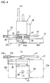
- the light emitter unit 35 has a through hole 39 bored through both light emitter 36 and diffusing plate 37 at the position corresponding to the first attracting nozzle 21 while the light emitter unit is at the first position (See Fig.4) so that the first attracting nozzle 21 may be inserted therein.
- Light emitter unit driving means 40 is provided to move the light emitter unit 35, and is constructed with a first cylinder 41 and a second cylinder 42. To the tip end portion of the rod of the first cylinder 41 are connected an expanded portion 41a and a shaft portion 41b.
- a bracket 43 is connected to the mounting member 38 of the light emitter unit 35 and is movably coupled with the shaft portion 41b, and is pushed against the expanded portion 41a by the urging force of a spring 44. Further, the extended potion of this bracket 43 is positioned opposite to the tip end of the rod of the second cylinder 42.
- the light emitter unit 35 When the first cylinder 41 is actuated and its rod is pushed out, the light emitter unit 35 is moved to its first position (component photographing position) at which the light emitter unit 35 covers the nozzle installiing portion from below. When the first cylinder 41 is actuated and its rod is pulled in, and the second cylinder is also in the state having its rod pulled in, the light emitter unit 35 is moved to the second position (optical detecting means operating position) away from the nozzle installing portion as shown in Figs.5(a) and 5(b).
- the light emitter unit 35 is moved to the third position (substrate photographing position) at whifh the through hole 39 corresponds to the substrate photographing camera 48 as shown in Figs.6(a) and 6(b).
- the head unit 5 is provided with position detecting means composed of three sensors for detecting a dog 45 provided on the light emitter unit 35 at each of the positions above.
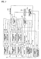
- Fig.7 shows an embodimnt of the control system.
- the Y axis servomotor 9, X axis servomotor 15, Z axis servomotors 23,24 and R axis servomotors 25,26 for attracting nozzles 21,22 of the head unit 5, and position detecting means 10,16,27 through 30 provided on these servomotors are electrically connected to the axis controller (driver) 51 of the main controller 50.
- the laser unit 31 is electrically connected to the laser unit processor 55, which is connected to the main processor 53 through the input/output means 52 of the main controller 50.
- position detecting means 46, light emitter unit driving means 40 and light emitter 36 for the light emitter unit 35 are connected to the input/output means 52.
- the substrate recognizing camera 48 equipped on the head unit 5 and the component recognizing camera 33 installed on the base 1 of the mounting machine are connected to the image processing section 54 provided in the main controller 50.
- the image processing section 54 reads the image of the chip component taken by the component recognizing camera 39 and processes the image as specified to detect the center position and rotating angle, etc., of the chip component when the chip component attracted state is detected on the basis of the image taken by the component recognizing camera 33. Further, the image processing section 54 reads the image sent from the substrate recognizing camera 48 and processes the image as specified to detect the mark attached on the substrate 3 when recognizing the substrate to detect the position of the substrate 3.
- the main processor 53 selects one from the laser unit 31 and the component recognizing camera 33 so as to be used for detecting the component attracted state according to the kind, etc., of the components while controlling the operations of servomotors 9,15,23 through 26 through the axis driver 51 so that attraction and mounting of components may be automatically carried out, and controls according to this selection. That is, the laser unit is selected when the component attracted state can be detected by the laser unit 31 and the component recognizing camera 33 is selected for a component the attracted state of which is difficult to be detected by the laser unit 31, for example, for chip components having many lead pins projecting therefrom, and processes for detecting the component attracted state and controls the light emitter unit driving means 40 according to such selection.
- the control by the main controller 50 is described referring to Figs.4 through 6 on the basis of flow charts of Figs.8 through 10.
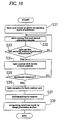
- Fig.8 shows a routine for detecting the component attracted state by the component recognizing camera.
- the first and second attracting nozzles are raised by the Z axis servomotors 23,24.
- the head unit 5 is moved to the component mounting position by the Y axis and X axis servomotors 9 and 15 at the step S5, and only the the first attracting nozzle 21 is lowered by the Z axis servomotor at the step S6.
- the through hole 39 is at the position corresponding to the first attracting nozzle 21 when the light emitter unit 35 is at the first position. the first nozzle 21 can be lowered through the through hole 39.
- a chip componet is attracted to the first attracting nozzle 21 at the step S7. Then, while the first attracting nozzle 21 is raised until the chip component attracted to the first attracting nozzle 21 reaches a height lower than the light emitter unit 35 and appropriate for photographing at the step S8, the head unit 5 is moved to a position above the component recognizing camera 33 at the step S9.
- the light emitter unit 35 emits light at the step S10, and the chip component is photographed by the component recognizing camera 33 at the steo S11.
- the chip component is recognized, the component attracted state is detected and the correction amount is obtained by the image processing section 54.
- the image of the chip component is scanned at the image processing section 54, the center position and the rotating angle about the R axis of the chip component are obtained on the basis of this scanning, and the correction amounts in the X, Y and rotational directions are obtained from the positional deviation of the component center point relative to the component attracting point of the attracting nozzle and the rotating angle deviation.
- the component is mounted at the step S13, that is, when the head unit is moved to a position above the substrate 3 and the attracting nozzle 21 reaches the corrected component mounting position, the attracting nozzle is lowered and the chip component is mounted on the substrate 3.
- the light emitter unit 35 is brought to the first position to make it possibe to recognize the component by photographing as shown also in Fig.4, only the first nozzle 21 among the attracting nozzles of the head unit 5 is used, and the chip component 20A is attracted and mounted by this attracting nozzle 21.
- the through hole 39 is at the position corresponding to the first nozzle 21, the attracting nozzle 21 can be raised/lowered through this hole 39 to attract and mount a chip component.
- the chip component 20A requiring component recognition by photographing is usually of larger size, if the first attracting nozzle 21 is disposed near the center of the domain corresponding to the space 32 above, there is no trouble even if the attacted component is of larger size.
- the attracted state of the component is detected by image processing on the basis of the image obtained by the component recognizing camera 33.
- the light emitter unit 35 constitutes a background for the chip component being photographed while functioning as a lighting, a clear image can be obtained.
- Fig.9 show the routine for detecting the component attracted state with the laser unit 31.
- the first and second attracting nozzles 21,22 are raised at the step S21, and, at the step S22, it is decided whether both nozzles 21,22 were raised into the range where the light emitter unit 35 is movable without interfering with both nozzles 21,22 or not, and, when this decision is yes, the light emitter unit 35 is moved to the second position at the step S23.
- the component is attracted at the step S25; that is, while the head unit 5 is moved to the component attracting position, both first and second attracting nozzles 21,22 are actuated and a chip component is attracted to each of both nozzles.
- the component is recognized (component attracted state is detected) by the laser unit 31, and the correction amounts are obtained.
- the process for example, while the chip components attracted to the attracting nozzles 21,22 are rotated in a state kept at a height position corresponding to the laser unit 31, laser beams are emitted from the laser beam generating section 31a, the projection width of the chip component is detected by the detector 31b receiving the laser beam above, and the correction amounts in the X axis, Y axis and rotational directions are obtained from the projection width, center point, rotation angle, etc., obtained at the position where the projection width becomes minimum.
- the components are mounted at the step S27.
- the light emitter unit is moved to the second position where the light emitter unit does not interfere with the up/down movement of both attracting nozzles 21,22 as shown also in Fig.5, and the chip components 20B are attracted and mounted by both attracting nozzles 21,22.
- the attracted states of the components are detected on the basis of the projection by the laser unit 31.
- the overall production efficiency is elevated.
- the production efficiency is elevated also because both of first and second attracting nozzles 21,22 are used.
- Fig. 10 shows the routine for substrate recognizing process.
- the head unit 5 is moved to a position above the recognizing mark attatched on the substrate.
- the first and second attracting nozzles 21,22 are raised at the step S32, and it is decided whether both nozzles 21,22 has been raised into the range where the light emitter unit 35 can be moved without interference with both nozzles 21,22 or not at the step S33.
- this decision is yes, the light emitter unit 35 is moved to the third position at the step S4.
- the light emitter unit 35 emits light at the step S36, and the substrate 3 is photographed in this state by the substrate recognizing camera 48 at the step S37. Then, at the step S38, the mark attached on the substrate 3 is recognized by image processing at the image processing section 54, and its position is detected.
- the mark of the substrate 3 is investigated by the substrate recognizing camera 48 installed on the head unit 5.
- the light emitter unit 35 is moved to the third position, and the through hole 39 is brought to the position corresponding to the substrate recognizing camera 48. In this state, the light emitter unit 35 is used as lighting for photographing the substrate 3.
- the practical structure of this invention can be variously modified from the embodiment above.
- the embodiment above is equipped with a light emitter unit 35 having a light emitter 36 and a diffusing plate 37 on the head unit 5
- another structure is possible in which the light emitter is installed on the base and a reflector plate is installed on the head unit so as to constitute a background for photographing the component.
- the embodiment above is provided with one first attracting nozzle 21 and one second attracting nozzle 22, and only the first nozzle 21 is used when the component recognizing camera is used while both attracting nozzles 21 and 22 are used when the laser unit is used, two or more second nozzles may be used when the laser unit is used, and, in such a case, the first nozzle may be used exclusively for the case where the component recognizing camera is used. Still further, the mounting machine may be provided with a plurality of first nozzles.
- the component attracted state detecting system for the component mounting machine is provided, in addition to optical detecting means for detecting the component attracted state on the basis of the projection, with photographing means for detecting the component attracted state on the basis of the photograph means for detecting the component attracted state on the basis of the photograph image so that the photographing means and optical detecting means may be used selectively, and it is possible to appropriately use the photographing means and the optical detecting means for detecting the component attracted state selectively according to the kind of components.
- the photographing assisting member may constitute a background for obtaining clear image while making the operation of the first nozzle possible.
- the optical detecting meas when used, a series of operations such as attraction of chip components, detection of component attracted state, component mounting, etc., can be carried out efficiently in the state with the photographing assisting member kept away from the nozzle installing portion so that it may not interfere the operation of each attracting nozzle.
- the head unit is provided with a first and second attracting nozzles and is said photographing assisting member having a portion constituting a background when photographing and a through hole bored at a specific position and photographing assisting member driving means for moving the photographing assisting member to the position for the component photographing or to the position for the optical detecting means.
- the photographing assisting member is provided with a light emitter, and the photographing assisting member is so constructed that the through hole thereof can be brought also to the position for substrate photographing corresponding to the substrate photographing means in this invention, the light emitter can be used for lighting both when photographing the component and when photographing the substrate, and the substrate can be photographed with a simple structure.
Abstract
Description
- The present invention relates to a method for mounting a minute component onto a substrate, said component being attracted by means of an attracting nozzle disposed on a head unit and is investigated as to its attracted state through a component attracted state detecting system. Moreover, the present invention relates to a component mounting machine for mounting such components, preferably for performing the afore-indicated method.
- For mounting minute component such as I.C's, resistors, transisters, condensers, etc., exactly on their specified positions on the substrate, such as a printed circuit board, mounting apparatuses were already suggested which attract a component through an attracting nozzle by vacuum and detecting the attracting position of the component in view of irregularities which can prevent the component from being precisely positioned on the desired spot onto the substrate. Such component mounting apparatuses are, for example, disclosed in the applicant's previous European patent applications No. 93111932.5, 93110535.7, 93110547.2 and 93110537.3 which all belong to the prior art under Article 54(3) EPC.
- Therefore, so far a chip component mounting machine as already been suggested on which a chip component, such as a electronic component like I.C., etc., is attracted from a component feeding section by a mounting head unit of the machine, transfered to a prepositioned substrate such as a printed circuit board and is mounted at a predetermined position thereon. Such a mounting machine usually has a head unit adapted for moving in the X-axis and Y-axis directions and at least one attracting nozzle adapted for moving in a Z-axis vertical direction. Moreover, the attracting nozzle is rotatable about its vertical R-axis and the head unit is provided with a driving means for movement in various directions and for rotating the attracting nozzle. By controlling these driving means and supply means for applying a negative pressure to the attracting nozzle, the chip component is automatically attracted and mounted.
- As the attracting position of the component as attracted to the attracting nozzle tends to imply some undesirable deviations, it is required to correct the mounting position according to the position of deviations of the component and, therefore, it has already been suggested to equip the mounting machine with an optical detecting means composed of a parallel light beam emitting section and a light receiving section for emitting parallel light beams toward the component and detecting the attracted state of the component on the basis of the projection of the component (see EP93110547.2).
- In some cases difficulties have arisen with said system as the components to be attracted and mounted have many lead pins projected therefrom which render sometimes a clear detection by the article detecting means difficult.
- Moreover, further problems may arise from the fact that it is desirable to provide the head unit with a plurality of attracting nozzles for improving the efficiency of the production. Depending on the size of the components which require recognition it is either desirable to attract and mount components by all of a plurality of attracting nozzles or by using only one or as selected number thereof. Moreover, attention is to be paid to avoid any interference between the components and the attracted state detecting means.
- Therefore, it is an objective of the present invention to provide a method for mounting minute components onto a substrate as indicated above which allows a more appropriate approach and adaption of the attracted state detecting system to the type of component to be investigated and instantaneously to be mounted. In other words it is desired to consider to a greater extend the nature and size of the component to be mounted when detecting and evaluating the attracted state of the component.
- Moreover, it is a further objective of the present invention to provide an improved component mounting machine as indicated above, particularly adapted for performing said method, having an improved detecting system for evaluating the attracted state of the component, said detecting system enabling to meet a different detecting requirements in response to a different type and nature or size of the component the attracted state of which is to be investigated.
- In order to perform the afore-indicated objective in terms of the method, the present invention improves the method for mounting a minute component onto a substrate in that the component is subject to an attracted state detecting investigation either through an optical detecting means or through a photographing means on the basis of a photograph according to a selection of said detecting means in response to the type of component to be mounted.
- According to a preferred embodiment of said method, a main processor of a main controller selects on of a laser unit (as the optical detecting means) and a component recognising camera (as the photographing means) to be used for detecting the component attracted state according to the type of the components while controlling the operations of several drive motors through an axis driver unit to automatically attract and mount said components according to the selection of the means for investigating the attracted state of the component.
- Further preferred developments of the method according to the present invention are laid down in the further subclaims.
- In order to perform the afore-indicated objective in terms of the component mounting machine as defined in the preamble of claim 8, the present invention improves said machine in that at least one photographing means is provided for detecting the component attracting state on the basis of a photograph.
- Preferably, said photographing means is a component recognising camera disposed on a base of the machine.
- Moreover, according to yet another preferred embodiment of the present invention, said photographing means comprising a photographing assisting member which at least partially constitutes a background for photographing, said photographing assisting member having a through hole for accommodating an attracting nozzle therethrough when photographing same.
- According to yet another preferred embodiment of said machine according to the present invention the head unit thereof is provided with a substrate photographing means for detecting the substrate on which the components are to be mounted and that the photographing assisting member is provided with light emitting members and that driving means for driving the photographing assisting means is provided for moving the photographing assisting member from a component photographing position to an operating position of the optical detecting means and to a substrate photographing position corresponding to the substrate photographing means.
- The component mounting machine according to this invention, thus, in addition to an optical detecting means for detecting the attracted state of a component on the basis of its projection, is equipped with a photographing means for detecting the attracted state of the component on the basis of a photograph image so that the photographing means and the optical detecting means may be used alternatively for detecting the attracted state of the component.
- Accordingly, the detecting means can be selected in response to the properties such as size and design of the component to be detected so that correction amounts for the positioning of the component onto the substrate can be more precisely obtained while a smooth interference-free cooperation of all components of the attracted state detecting system as well as of a preferably added substrate recognition system can be assured.
- Further preferred embodiments of the component mounting machine according to this invention are laid down in the other subclaims.
- With the afore-indicated method and components mounting machine, in its most developed state including all preferred embodiments thereof, when a series of operations of component attraction, attracted state detection, component mounting, etc., are carried out, it is decided which of the photographing means and the optical detecting means is to be used for detecting the component attracted state according to the kind of the component. When the photographing means is used, a preferably provided photographing assisting member constitutes a background for photographing by being brought to the position for component photographing, and, in this state, a through hole of the photographing assisting member allows the first attracting nozzle to move up and down, and a chip component is attracted and mounted by the first attracting nozzle. On the other hand, when the optical detecting means is used, a chip component is attracted and mounted preferably also by the second attracting nozzle with the photographing means kept away from the nozzle installing portion.
- Further, if the preferably provided photographing assisting member is provided with a light emitter and is adapted for being moved to the position for photographing the substrate when photographing the substrate by the substrate photographing means installed on the head unit, a light emitter preferably installed on the photographing assisting means is used for lighting both when photographing the component and for photographing the substrate.
- In the following the present invention is explained in greater detail through an embodiment thereof in conjunction with the accompanying drawings, wherein:
- Figure 1 is an overall plan view of a component mounting machine according a preferred embodiment of this invention, having detecting means for investigating a component attracted state,
- Figure 2 is a front view of the component mounting machine of Figure 1,
- Figure 3 is an enlarged front view of a head unit of the component mounting machine of Figures 1 and 2,
- Figure 4a and 4b show the state of the head unit in the case where a component recognising camera is used for detecting the component attracted state with Figure 4a being a schematic front view and Figure 4b being a schematic plan view,
- Figures 5a and 5b show the state of a head unit in the case where a laser unit is used for detecting the component attracted state with Figure 5a being a schematic front view and Figure 5b being a schematic plan view,
- Figure 6a and 6b show the state of a head unit while recognising a substate with Figure 6a being a schematic front view and Figure 6b being a schematic plan view,
- Figure 7 is a block diagram of a control system of the component mounting machine of Figure 1,
- Figure 8 is a flow chart showing the control in the case where a component recognising camera is used for detecting the attracted state of the component,
- Figure 9 is a flow chart showing the control in the case where a laser unit is used for detecting the attracted state of the component,
- Figure 10 is a flow chart showing the control for recognising a substrate.
- An embodiment of this invention is described referring to appended drawings. Fig.1 and Fig.2 show the overall structure of a component mounting machine, an embodiment of this invention. As shown, a
conveyer 2 for conveying printed substrates is inastalled on thebase 1, the printed substrate is conveyed on theconveyer 2, and is brought to a stop at a predetermined component mounting position. - On the sides of the
conveyer 2 are disposedcomponent feeding sections 4 each provided with many rows oftape feeders 4a. Eachtape feeder 4a is adapted for sending out a tape holidng and containing chip components 20 such as I.C's, transisters, condensers, etc., at regular intervals from a reel, and is provided with a ratchet type feeder mechanism incorporated at the tape send-out end so that thefeeder tape 4a may be intermittently sent out as chip components are picked up by ahand unit 5 to be described later. - The
head unit 5 adapted for moving both in the X axis direction (direction of the conveyer 2) and in the Y axis direction (direction perpendiclar to the X axis direction on a horizontal plane) is installed above thebase 1. - That is, while a pair of
fixed rails 7 extended in the Y axis direction and a ball screw 8 to be rotated by aY axis servomotor 9 are disposed on thebase 1, a headunit support member 11 is supported on thefixed rails 7, and anut portion 12 provided on thesupport member 11 is in screw-engagement with the ball screw 8. The supportingmember 11 is provided with aguide member 13 extended in the X-axis direction and a ball screw 14 to be rotated by anX axis servomotor 15, ahead unit 5 is movably supported by saidguide member 13, and a nut portion (not shown) provided in thishead unit 5 is in screw-engagement with the ball screw 14. While the ball screw 8 is rotated by the operation of theY axis servomotor 9 and thesupport member 11 is moved in the Y axis direction, the ball screw 14 is rotated by the operation of theX axis servomotor 15 and thehead unit 5 is moved in the X axis direction relative to thesupport member 11. - The
Y axis servomotor 9 andX axis servomotor 15 are respectively provided with position detecting means 10 and 16 each constituted of an encoder. - The
head unit 5 is provided with first and second attractingnozzles laser unit 31 as optical detecting means for detecting the attracted state of the chip components on the basis of the projection, acomponent recognizing camera 33 as photographing means is installed at a suitable position within the head unit moving range on thebase 1. Further, thehead unit 5 is equipped with alight emitter unit 35 as a photographing assisting member and asubstrate recognizing camera 48 as substrate photographing means. - Concretely describing members equipped on the
head unit 5 referring to Fig.3, both attractingnozzles Z axis servomotors R axis servomotors servomotor 23 through 26 is provided with a positiion detecting means 27 through 30, respectively. Each attractingnozzle - The first attracting
nozzle 21 is used for component attraction in both cases where the component attracted state is detected by thelaser unit 31 and where the component attracted state is detected by thecomponent recognizing camera 33, and is disposed generally at the center of the space corresponding to thespace 32 in thelaser unit 31. The second attractingnozzle 22 is used for component attraction only in the case where the component attracted state is detected by thelaser unit 31, and is disposed slantly on one side of thefirst nozzle 21. - On the lower end portion of the
head unit 5 is installed thelaser unit 31. Thislaser unit 31 has a laser beam generating section (parallel beam emitting section) 31a and a detector (light receiving section) 31 disposed opposite to each other on both sides of aspace 32 through which the attractingnozzles detector 31b is constituted of a CCD. - The
light emitter unit 35 is disposed on the lower portion of thehead unit 5 above thelaser unit 31. Thislight emitter unit 35 has a plate-like light emitter 36 composed of a number of LEDs, adiffusing plate 37 positioned under thelight emitter 36 and amounting member 38 for combining these 36 and 37. The diffusing plate constitutes a background for photographing the chip component attracted to the attractingnozzle 21, and is constructed with milk white acril plates, etc., so that the light from thelight emitter 36 may be diffused. - This
light emitter unit 35 is mounted so as to be movable in the lateral direction relative to the head unit 5 (left-right direction in Fig.3). Thelight emitter unit 35 has a throughhole 39 bored through bothlight emitter 36 and diffusingplate 37 at the position corresponding to the first attractingnozzle 21 while the light emitter unit is at the first position (See Fig.4) so that the first attractingnozzle 21 may be inserted therein. - Light emitter unit driving means 40 is provided to move the
light emitter unit 35, and is constructed with afirst cylinder 41 and asecond cylinder 42. To the tip end portion of the rod of thefirst cylinder 41 are connected an expandedportion 41a and ashaft portion 41b. Abracket 43 is connected to the mountingmember 38 of thelight emitter unit 35 and is movably coupled with theshaft portion 41b, and is pushed against the expandedportion 41a by the urging force of aspring 44. Further, the extended potion of thisbracket 43 is positioned opposite to the tip end of the rod of thesecond cylinder 42. - When the
first cylinder 41 is actuated and its rod is pushed out, thelight emitter unit 35 is moved to its first position (component photographing position) at which thelight emitter unit 35 covers the nozzle installiing portion from below. When thefirst cylinder 41 is actuated and its rod is pulled in, and the second cylinder is also in the state having its rod pulled in, thelight emitter unit 35 is moved to the second position (optical detecting means operating position) away from the nozzle installing portion as shown in Figs.5(a) and 5(b). Further, when thefirst cylinder 41 is in the state having its rod pulled in and the second cylinder is in the state having its rod pushed out, thelight emitter unit 35 is moved to the third position (substrate photographing position) at whifh the throughhole 39 corresponds to thesubstrate photographing camera 48 as shown in Figs.6(a) and 6(b). - To detect these three positions, the
head unit 5 is provided with position detecting means composed of three sensors for detecting adog 45 provided on thelight emitter unit 35 at each of the positions above. - Fig.7 shows an embodimnt of the control system. In this diagram, the
Y axis servomotor 9,X axis servomotor 15,Z axis servomotors R axis servomotors nozzles head unit 5, and position detecting means 10,16,27 through 30 provided on these servomotors are electrically connected to the axis controller (driver) 51 of themain controller 50. Thelaser unit 31 is electrically connected to thelaser unit processor 55, which is connected to themain processor 53 through the input/output means 52 of themain controller 50. Further, position detecting means 46, light emitter unit driving means 40 andlight emitter 36 for thelight emitter unit 35 are connected to the input/output means 52. - The
substrate recognizing camera 48 equipped on thehead unit 5 and thecomponent recognizing camera 33 installed on thebase 1 of the mounting machine are connected to theimage processing section 54 provided in themain controller 50. Theimage processing section 54 reads the image of the chip component taken by thecomponent recognizing camera 39 and processes the image as specified to detect the center position and rotating angle, etc., of the chip component when the chip component attracted state is detected on the basis of the image taken by thecomponent recognizing camera 33. Further, theimage processing section 54 reads the image sent from thesubstrate recognizing camera 48 and processes the image as specified to detect the mark attached on the substrate 3 when recognizing the substrate to detect the position of the substrate 3. - The
main processor 53 selects one from thelaser unit 31 and thecomponent recognizing camera 33 so as to be used for detecting the component attracted state according to the kind, etc., of the components while controlling the operations ofservomotors axis driver 51 so that attraction and mounting of components may be automatically carried out, and controls according to this selection. That is, the laser unit is selected when the component attracted state can be detected by thelaser unit 31 and thecomponent recognizing camera 33 is selected for a component the attracted state of which is difficult to be detected by thelaser unit 31, for example, for chip components having many lead pins projecting therefrom, and processes for detecting the component attracted state and controls the light emitter unit driving means 40 according to such selection. - The control by the
main controller 50 is described referring to Figs.4 through 6 on the basis of flow charts of Figs.8 through 10. - Fig.8 shows a routine for detecting the component attracted state by the component recognizing camera. In this routine, at the step S1, the first and second attracting nozzles are raised by the
Z axis servomotors nozzles light emitter unit 35 is movable without interfering with bothnozzles light emitter unit 35 is moved to the first position at the step S3. Then, when it is decided that the movemnt of thelight emitter unit 35 has been completed at the step S4, thehead unit 5 is moved to the component mounting position by the Y axis andX axis servomotors nozzle 21 is lowered by the Z axis servomotor at the step S6. In this case, since the throughhole 39 is at the position corresponding to the first attractingnozzle 21 when thelight emitter unit 35 is at the first position. thefirst nozzle 21 can be lowered through the throughhole 39. - After lowering above, a chip componet is attracted to the first attracting
nozzle 21 at the step S7. Then, while the first attractingnozzle 21 is raised until the chip component attracted to the first attractingnozzle 21 reaches a height lower than thelight emitter unit 35 and appropriate for photographing at the step S8, thehead unit 5 is moved to a position above thecomponent recognizing camera 33 at the step S9. - Then, the
light emitter unit 35 emits light at the step S10, and the chip component is photographed by thecomponent recognizing camera 33 at the steo S11. At the step S12, the chip component is recognized, the component attracted state is detected and the correction amount is obtained by theimage processing section 54. As the process here,the image of the chip component is scanned at theimage processing section 54, the center position and the rotating angle about the R axis of the chip component are obtained on the basis of this scanning, and the correction amounts in the X, Y and rotational directions are obtained from the positional deviation of the component center point relative to the component attracting point of the attracting nozzle and the rotating angle deviation. - Next. the component is mounted at the step S13, that is, when the head unit is moved to a position above the substrate 3 and the attracting
nozzle 21 reaches the corrected component mounting position, the attracting nozzle is lowered and the chip component is mounted on the substrate 3. - With such a process as shown in Fig.8, the
light emitter unit 35 is brought to the first position to make it possibe to recognize the component by photographing as shown also in Fig.4, only thefirst nozzle 21 among the attracting nozzles of thehead unit 5 is used, and thechip component 20A is attracted and mounted by this attractingnozzle 21. In this case, since the throughhole 39 is at the position corresponding to thefirst nozzle 21, the attractingnozzle 21 can be raised/lowered through thishole 39 to attract and mount a chip component. Although thechip component 20A requiring component recognition by photographing is usually of larger size, if the first attractingnozzle 21 is disposed near the center of the domain corresponding to thespace 32 above, there is no trouble even if the attacted component is of larger size. - After the component is attracted, the attracted state of the component is detected by image processing on the basis of the image obtained by the
component recognizing camera 33. In this case, since thelight emitter unit 35 constitutes a background for the chip component being photographed while functioning as a lighting, a clear image can be obtained. - Fig.9 show the routine for detecting the component attracted state with the
laser unit 31. In this routine, first, the first and second attractingnozzles nozzles light emitter unit 35 is movable without interfering with bothnozzles light emitter unit 35 is moved to the second position at the step S23. Then, when it is confirmed at the step S24 that the movement of thelight emitter unit 35 has been completed, the component is attracted at the step S25; that is, while thehead unit 5 is moved to the component attracting position, both first and second attractingnozzles - Then, at the step S26, the component is recognized (component attracted state is detected) by the
laser unit 31, and the correction amounts are obtained. As the process here, for example, while the chip components attracted to the attractingnozzles laser unit 31, laser beams are emitted from the laserbeam generating section 31a, the projection width of the chip component is detected by thedetector 31b receiving the laser beam above, and the correction amounts in the X axis, Y axis and rotational directions are obtained from the projection width, center point, rotation angle, etc., obtained at the position where the projection width becomes minimum. After this process, the components are mounted at the step S27. - With such a process as shown in Fig.9, the light emitter unit is moved to the second position where the light emitter unit does not interfere with the up/down movement of both attracting
nozzles chip components 20B are attracted and mounted by both attractingnozzles - After the components are attracted, the attracted states of the components are detected on the basis of the projection by the
laser unit 31. - Since this process is continued also while the
head unit 5 is moved from thecomponent feeding section 4 to the position above the substrate, the overall production efficiency is elevated. The production efficiency is elevated also because both of first and second attractingnozzles - Fig. 10 shows the routine for substrate recognizing process. In this routine, first, at the step S31, the
head unit 5 is moved to a position above the recognizing mark attatched on the substrate. Then, the first and second attractingnozzles nozzles light emitter unit 35 can be moved without interference with bothnozzles light emitter unit 35 is moved to the third position at the step S4. Then, when it is confirmed at the step S35 that the movement of thelight emitter unit 35 has been completed, the light emitter unit emits light at the step S36, and the substrate 3 is photographed in this state by thesubstrate recognizing camera 48 at the step S37. Then, at the step S38, the mark attached on the substrate 3 is recognized by image processing at theimage processing section 54, and its position is detected. - With such a substrate recognizing process as shown in Fig.10, the mark of the substrate 3 is investigated by the
substrate recognizing camera 48 installed on thehead unit 5. In this case, as shown also in Fig.6, thelight emitter unit 35 is moved to the third position, and the throughhole 39 is brought to the position corresponding to thesubstrate recognizing camera 48. In this state, thelight emitter unit 35 is used as lighting for photographing the substrate 3. - The practical structure of this invention can be variously modified from the embodiment above. For example, although the embodiment above is equipped with a
light emitter unit 35 having alight emitter 36 and a diffusingplate 37 on thehead unit 5, another structure is possible in which the light emitter is installed on the base and a reflector plate is installed on the head unit so as to constitute a background for photographing the component. - Although the embodiment above is provided with one first attracting
nozzle 21 and one second attractingnozzle 22, and only thefirst nozzle 21 is used when the component recognizing camera is used while both attractingnozzles - Since the component attracted state detecting system for the component mounting machine according to this invention is provided, in addition to optical detecting means for detecting the component attracted state on the basis of the projection, with photographing means for detecting the component attracted state on the basis of the photograph means for detecting the component attracted state on the basis of the photograph image so that the photographing means and optical detecting means may be used selectively, and it is possible to appropriately use the photographing means and the optical detecting means for detecting the component attracted state selectively according to the kind of components.
- Especially when the photographing means is used, the photographing assisting member may constitute a background for obtaining clear image while making the operation of the first nozzle possible.
- On the other hand, when the optical detecting meas is used, a series of operations such as attraction of chip components, detection of component attracted state, component mounting, etc., can be carried out efficiently in the state with the photographing assisting member kept away from the nozzle installing portion so that it may not interfere the operation of each attracting nozzle.
- Preferably, the head unit is provided with a first and second attracting nozzles and is said photographing assisting member having a portion constituting a background when photographing and a through hole bored at a specific position and photographing assisting member driving means for moving the photographing assisting member to the position for the component photographing or to the position for the optical detecting means.
- Further, if the head unit is provided with substrate photographing means, the photographing assisting member is provided with a light emitter, and the photographing assisting member is so constructed that the through hole thereof can be brought also to the position for substrate photographing corresponding to the substrate photographing means in this invention, the light emitter can be used for lighting both when photographing the component and when photographing the substrate, and the substrate can be photographed with a simple structure.
Claims (23)
- Method for mounting a minute component onto a substrate, said component being attracted by means of an attracting nozzle disposed on a head unit (5) and investigated as to its attracted state through a component attracted state detecting system characterised in that the component (20A,20B) is subject to an attracted state detecting investigation either through a optical detecting means (31) or a photographing means (33) on the basis of a photograph according to a selection of said detecting means in response to the type of component (20A,20B) to be mounted.
- Method for mounting a component as claimed in claim 1 characterised in that a main processor (53) of a main controller (50) selects one of a laser unit (31) and a component recognising camera (33) to be used for detecting the component attracted state according to the type of the components (20A,20B) while controlling the operations of several motors (9,15,23 to 26) through an axis driver unit (51) to automatically attract and mount said components according to the selection of the means for investigating the attracted state of the component (20A,20B).
- Method for mounting a component as claimed in claims 1 or 2, characterised in that, the detection of the component attracting state by the component recognising camera (33) comprises raising of a first and second attracting nozzle (21,22) by respective vertical Z-axis servo motors (23,24), moving a light beam emitting unit (35) as photographing assisting means in a first photographing assisting position, moving the head unit (5) by operating Y-axis and X-axis servo motors (9,15) to the component mounting position and lowering the first attracting nozzle (21) only through the associated Z-axis servo motor (23) to insert the first attracting nozzle (21) into a through hole (39) of the light beam emitting unit (35) to attract a chip component (20A), then raising the first nozzle (21) until the chip component (20A) attracted to the first attracted nozzle (21) reaching a height lower than that of light beam emitting unit (35) appropriate for photographing while the head unit (5) is moved then to a position above the component recognising camera (33) and, on the light emission through the light beam emitting unit (35), the component (20A) is photographed by the component recognising camera (33).
- Method for mounting a component as claimed in claim 3, characterised in that, the component (20A) is recognised, the component attracted state is detected and an correction amount for positioning the component (20A) on the substrate is obtained by the image processing section (54) of the main controller (50).
- Method for mounting a component as claimed in claim 20, characterised in that, an image of the component (20A) is scanned at the image processing section (54), a centre position and a rotating angle about the R-axis of the component (20A) are obtained on the basis of said scanning and correction amounts of the X-,Y- and rotational directions are obtained from the positional deviation of a component centre point relative to a component attracting point of the attracting nozzle (21) and a deviation of the rotating angle.
- Method for mounting a component as claimed in claim 19 or 20, characterised in that a detection of the component attracting state by the optical detecting means comprises raising of the first and second attracting nozzles (21,22), moving the light beam emitting unit (35) to a second operating position of the optical detecting means (31), moving the head unit (5) to the component attracting position actuating both first and second attracting nozzles (21,22) and attracting components (20A,20B) to each of said attracting nozzles (21,22), recognising the components (21,22) by the optical detecting means (31) and obtaining correction amounts, preferably while the components (20A,20B) attracted to the attracting nozzles (21,22) are rotated in a state kept at a height position corresponding to the height of the optical detecting means (31) and emitting laser beams from the laser beam generating section (31a) detecting the projection width of the chip components (20A,20B) by the light beam receiving section (31b) and obtaining correction amounts in the X-axis, Y-axis and rotational directions at the position where the projection width becomes minimal.
- Method for mounting a component as claimed in at least one of the preceeding claims 1 to 6 characterised in that, a substrate recognising process is carried out moving the head unit (5) to a position above a recognising mark attached onto the substrate, raising the first and second attracting nozzles (21,22) moving the photographing assisting means comprising the light beam emitting unit (35) to a third position to emit light onto the substrate (3), photographing the lightened substrate (3) by a substrate recognising camera (48) and recognising by image processing at the image processing section (54) of the main controller (50) the position of the mark attached on the substrate (3).
- Component mounting machine comprising a moveable head unit (5) supporting a plurality of attracting nozzles (21,22) for attracting by vacuum at least one component (20A,20B) to be mounted, for mounting said component (20A,20B) at a predetermined position onto a substrate, specifically onto a printed circuit board, said head unit (5) comprising a detecting system (31) for detecting the attracted state of the electrical or electronic components (20B,20B) to said attracting nozzles (21,22), particularly for perfoming the method as claimed in claim 1, characterised in that at least one photographing means (33) is provided for detecting the component attracting state on the basis of a photograph.
- Component mounting machine as claimed in claim 8, characterised in that, said photographing means is a component recognising camera (33) disposed on a base (1) of the machine.
- Component mounting machine as claimed in claims 8 and 9, characterised in that, the detecting means is a optical detecting means (31) and that said optical detecting means (31) and said photographing means (33) being alternatively used to detect the attracted state of the component (20A,20B) at a selected attracting nozzle (21,22).
- Component mounting machine as claimed in at least one of the preceeding claims 8 to 10, characterised in that, said head unit (5) comprises at least one first attracting nozzle (21) and at least one second attracting nozzle (22), said second attracting nozzle (22) being exclusively used when said photographing means (33) is used to detect the attracted state of the component (20A, 20B).
- Component mounting machine as claimed in claim 4, characterised in that, said attracting nozzles (20A,20B) being moveable together with the head unit (5) in the directions of a X- or Y-axis defining a horizontal plane and being independently moveable in a vertical Z-axis direction while each of said attracting nozzles (21,22) being independently rotatable about its vertical axis (R).
- Component mounting machine as claimed in at least one the preceeding claims 8 to 12, characterised in that, said photographing means (33) comprising a photographing assisting member (35,36,37,38) which at least partially constitutes a background for photographing, said photographing assisting member (35,36,37,38) having a through hole (39) for accommodating an attracting nozzle (21) when photographing same.
- Component mounting machine as claimed in claim 13, characterised in that a driving means (40,41,42) for driving the photographing assisting means (35,36,37,38) is provided for moving the photographing assisting member (35,36,37,38) from a component photographing position covering a nozzle installation portion of the head unit (5) from below to an operating position of the optical detecting means (31) in which the photographing assisting member (35,36,37,38) is kept away from said nozzle installation portion of the head unit (5), or vice versa.
- Component mounting machine as claimed in at least one of the preceeding claims 8 to 14, characterised in that, said optical detecting means (31) being provided at the head unit (5) and comprises a parallel light beam emitting section (31a) and a light beam receiving section (31b) for detecting the attracted state of the component (20A,20B) on the basis of the detection of a projection of said component (20A,20B), specifically chip component, attracted to the attracting nozzle (21,22), respectively.
- Component mounting machine as claimed in claim 15, characterised in that, said optical detecting means comprises a laser unit (31).
- Component mounting machine as claimed in claim 13, characterised in that, said photographing assisting means comprises a moveable light beam emitting unit (35) having a plate like light emitter (36) composed of a plurality of LED's, a diffusing plate (37) positioned on the light emitter (36) and a mounting member (38) for combining the light emitter (36) and the diffusing plate (37).
- Component mounting machine as claimed in at least one of the preceeding claims 8 to 17, characterised in that, another photographing means (48) for photographing the substrate is provided.
- Component mounting machine as claimed in claim 18, characterised in that, said substrate photographing means (48) is supported through the head unit (5).
- Component mounting machine as claimed in at least one of the peceeding claims 13 to 19, characterised in that, said photographing assisting member (35,36,37,38) is adapted to be moved towards a substrate photographing position through its driving means (40,41,42), said substrate photographing position corresponds to a position of the substrate photographing means (48).
- Component mounting machine as claimed in at least one of the preceeding claims 8 to 20, characterised in that, the head unit (5) slideably and rotatably supports one first attracting nozzle (21) and one second attracting nozzle (22) disposed substantially parallel to each other supports the laser unit (31) as optical detecting means for detecting the attracted state of the chip components (20A,20B) on the basis of their projection, the photographing assisting means (35,36,37,38) including the light beam emitting unit (35) and the substrate recognising camera (48) as substrate photographing means.
- Component mounting machine as claimed in at least one of the preceeding claims 8 to 21, characterised in that, a control system is provided comprising a main controller (50) which comprises an axis controller driver circuit (51), input/output means (52), a main processor (53) and an image processing section (54).
- Component mounting machine as claimed in claim 22 characterised in that, the substrate recognising camera (48) equipped on the head unit (5) and the component recognising camera (33) installed on the base (1) of the mounting machine are connected to the image processing section (54) of the main controller (50).
Priority Applications (1)
| Application Number | Priority Date | Filing Date | Title |
|---|---|---|---|
| EP96106676A EP0730397B1 (en) | 1992-11-05 | 1993-11-05 | Method for mounting components on a substrate and components mounting machine therefor |
Applications Claiming Priority (2)
| Application Number | Priority Date | Filing Date | Title |
|---|---|---|---|
| JP296124/92 | 1992-11-05 | ||
| JP4296124A JP2554431B2 (en) | 1992-11-05 | 1992-11-05 | Mounting device component suction state detection device |
Related Child Applications (1)
| Application Number | Title | Priority Date | Filing Date |
|---|---|---|---|
| EP96106676A Division EP0730397B1 (en) | 1992-11-05 | 1993-11-05 | Method for mounting components on a substrate and components mounting machine therefor |
Publications (2)
| Publication Number | Publication Date |
|---|---|
| EP0596533A1 true EP0596533A1 (en) | 1994-05-11 |
| EP0596533B1 EP0596533B1 (en) | 1998-04-29 |
Family
ID=17829452
Family Applications (2)
| Application Number | Title | Priority Date | Filing Date |
|---|---|---|---|
| EP93118009A Expired - Lifetime EP0596533B1 (en) | 1992-11-05 | 1993-11-05 | Method for mounting components on a substrate and component mounting machine therefor |
| EP96106676A Expired - Lifetime EP0730397B1 (en) | 1992-11-05 | 1993-11-05 | Method for mounting components on a substrate and components mounting machine therefor |
Family Applications After (1)
| Application Number | Title | Priority Date | Filing Date |
|---|---|---|---|
| EP96106676A Expired - Lifetime EP0730397B1 (en) | 1992-11-05 | 1993-11-05 | Method for mounting components on a substrate and components mounting machine therefor |
Country Status (4)
| Country | Link |
|---|---|
| US (1) | US5839186A (en) |
| EP (2) | EP0596533B1 (en) |
| JP (1) | JP2554431B2 (en) |
| DE (2) | DE69324382T2 (en) |
Cited By (8)
| Publication number | Priority date | Publication date | Assignee | Title |
|---|---|---|---|---|
| WO1996012396A1 (en) * | 1994-10-12 | 1996-04-25 | Mydata Automation Ab | Reproduction of components |
| WO1996012395A1 (en) * | 1994-10-12 | 1996-04-25 | Mydata Automation Ab | Compact reproduction of components |
| EP0725560A2 (en) * | 1995-02-02 | 1996-08-07 | Yamaha Hatsudoki Kabushiki Kaisha | Mounting device for mounting electric and/or electronic parts |
| WO1997032180A1 (en) * | 1996-02-19 | 1997-09-04 | Philips Electronics N.V. | Device comprising diffuse foreground illumination for detecting an electronic component, and component-mounting machine provided with such a detection device |
| WO1998041078A1 (en) * | 1997-03-12 | 1998-09-17 | Matsushita Electric Industrial Co., Ltd. | Electronic component mounting apparatus |
| CN1096223C (en) * | 1995-11-06 | 2002-12-11 | 松下电器产业株式会社 | Component mounting apparatus and method, and component mounting equipment |
| US6862803B2 (en) * | 2000-08-29 | 2005-03-08 | Matsushita Electric Industrial Co., Ltd. | Method for mounting electronic component |
| EP1548396A1 (en) * | 2002-08-08 | 2005-06-29 | Matsushita Electric Industrial Co., Ltd. | Illumination device, recognizing device with the illumination device, and part mounting device |
Families Citing this family (36)
| Publication number | Priority date | Publication date | Assignee | Title |
|---|---|---|---|---|
| WO1997040657A1 (en) * | 1996-04-23 | 1997-10-30 | Matsushita Electric Industrial Co., Ltd. | Electronic component mounting apparatus |
| JPH1154993A (en) * | 1997-08-01 | 1999-02-26 | Yamagata Casio Co Ltd | Component mounting device |
| KR20000021713A (en) * | 1998-09-30 | 2000-04-25 | 윤종용 | Apparatus and method for mounting electronic parts |
| WO2000026640A1 (en) | 1998-11-05 | 2000-05-11 | Cyberoptics Corporation | Electronics assembly apparatus with improved imaging system |
| US6538244B1 (en) | 1999-11-03 | 2003-03-25 | Cyberoptics Corporation | Pick and place machine with improved vision system including a linescan sensor |
| JP2001338935A (en) * | 2000-05-26 | 2001-12-07 | Nidec Copal Corp | Die bonding apparatus |
| US6535291B1 (en) | 2000-06-07 | 2003-03-18 | Cyberoptics Corporation | Calibration methods for placement machines incorporating on-head linescan sensing |
| KR20010114161A (en) * | 2000-06-21 | 2001-12-29 | 마츠시타 덴끼 산교 가부시키가이샤 | Device and method for mounting parts |
| US7043820B2 (en) * | 2001-07-27 | 2006-05-16 | Fuji Machine Mfg. Co., Ltd. | Electric-component mounting system |
| DE10149780B4 (en) * | 2001-10-09 | 2019-09-05 | Byk Gardner Gmbh | Device for illuminating a measuring surface and device and method for determining the visual properties of bodies |
| US7239399B2 (en) * | 2001-11-13 | 2007-07-03 | Cyberoptics Corporation | Pick and place machine with component placement inspection |
| US7813559B2 (en) | 2001-11-13 | 2010-10-12 | Cyberoptics Corporation | Image analysis for pick and place machines with in situ component placement inspection |
| US7555831B2 (en) | 2001-11-13 | 2009-07-07 | Cyberoptics Corporation | Method of validating component feeder exchanges |
| JP3973439B2 (en) * | 2002-02-07 | 2007-09-12 | 松下電器産業株式会社 | Electronic component mounting apparatus and method |
| CN1303860C (en) * | 2002-04-01 | 2007-03-07 | 富士机械制造株式会社 | Working system for substrate |
| TW200419640A (en) * | 2003-02-25 | 2004-10-01 | Matsushita Electric Ind Co Ltd | Electronic component placement machine and electronic component placement method |
| JP4044017B2 (en) * | 2003-04-22 | 2008-02-06 | 松下電器産業株式会社 | Component mounting apparatus and method |
| KR20060073542A (en) * | 2003-07-03 | 2006-06-28 | 아셈블레온 엔. 브이. | Component placement device |
| JP4408682B2 (en) * | 2003-10-31 | 2010-02-03 | 株式会社日立ハイテクインスツルメンツ | Electronic component mounting device |
| US7559134B2 (en) | 2003-11-04 | 2009-07-14 | Cyberoptics Corporation | Pick and place machine with improved component placement inspection |
| US20050125993A1 (en) * | 2003-11-07 | 2005-06-16 | Madsen David D. | Pick and place machine with improved setup and operation procedure |
| US7706595B2 (en) | 2003-11-07 | 2010-04-27 | Cyberoptics Corporation | Pick and place machine with workpiece motion inspection |
| US20060016066A1 (en) * | 2004-07-21 | 2006-01-26 | Cyberoptics Corporation | Pick and place machine with improved inspection |
| JP4330512B2 (en) * | 2004-10-08 | 2009-09-16 | パナソニック株式会社 | Component mounting equipment |
| JP4896136B2 (en) | 2005-09-14 | 2012-03-14 | サイバーオプティクス コーポレーション | Pick and place machine with improved component pick image processing |
| EP1941536B8 (en) * | 2005-10-26 | 2019-06-19 | Kulicke and Soffa (Switzerland) Management GmbH | Method and device for the placement of electronic components, in particular semiconductor chips, on a substrate |
| JP4733499B2 (en) * | 2005-10-31 | 2011-07-27 | 株式会社日立ハイテクインスツルメンツ | Electronic component mounting device |
| JP4811073B2 (en) * | 2006-03-22 | 2011-11-09 | パナソニック株式会社 | Electronic component mounting apparatus and electronic component mounting method |
| US20070276867A1 (en) * | 2006-05-23 | 2007-11-29 | David Fishbaine | Embedded inspection image archival for electronics assembly machines |
| DE112007002690T5 (en) | 2006-11-06 | 2009-09-10 | Panasonic Corp., Kadoma | Movement device and assembly device for electronic components |
| JP4809799B2 (en) * | 2007-03-30 | 2011-11-09 | ヤマハ発動機株式会社 | Mounting machine, mounting method thereof, and moving method of board imaging means in mounting machine |
| NL1036851C2 (en) * | 2009-04-14 | 2010-10-18 | Assembléon B V | DEVICE SUITABLE FOR PLACING A COMPONENT ON A SUBSTRATE AND SUCH METHOD. |
| JP5584651B2 (en) * | 2011-05-12 | 2014-09-03 | ヤマハ発動機株式会社 | Adsorption state inspection device, surface mounter and component testing device |
| US8824166B2 (en) | 2011-08-31 | 2014-09-02 | Apple Inc. | Magnetic stand for tablet device |
| JP5816113B2 (en) * | 2012-03-05 | 2015-11-18 | Juki株式会社 | Component mounting equipment |
| JP7228075B2 (en) * | 2020-02-21 | 2023-02-22 | 株式会社Fuji | Parts mounting machine |
Citations (1)
| Publication number | Priority date | Publication date | Assignee | Title |
|---|---|---|---|---|
| EP0416878A1 (en) * | 1989-09-06 | 1991-03-13 | Matsushita Electric Industrial Co., Ltd. | Electronic component apparatus and method of mounting electronic component |
Family Cites Families (19)
| Publication number | Priority date | Publication date | Assignee | Title |
|---|---|---|---|---|
| DE3340084C2 (en) * | 1983-11-05 | 1985-10-31 | Zevatech AG, Bellach | Device for positioning components on a workpiece |
| JP2537770B2 (en) * | 1984-08-31 | 1996-09-25 | 松下電器産業株式会社 | How to mount electronic components |
| JPH0760448B2 (en) * | 1985-08-23 | 1995-06-28 | 松下電器産業株式会社 | Component position recognition device in component mounting machine |
| US4797994A (en) * | 1986-04-22 | 1989-01-17 | Kulicke & Soffa Industries, Inc. | Apparatus for and methods of die bonding |
| JPH0797019B2 (en) * | 1986-06-12 | 1995-10-18 | 松下電器産業株式会社 | Illumination method and device for component recognition |
| JPS63168097A (en) * | 1986-12-29 | 1988-07-12 | 株式会社東芝 | Electronic parts mounter |
| JPS63283100A (en) * | 1987-05-14 | 1988-11-18 | Seiko Epson Corp | Automatic mounting device for electronic component |
| JPH0236598A (en) * | 1988-07-27 | 1990-02-06 | Matsushita Electric Ind Co Ltd | Packaging of electronic component |
| JPH0380600A (en) * | 1989-08-24 | 1991-04-05 | Toshiba Corp | Electronic component inspection device |
| JP2808726B2 (en) * | 1989-09-26 | 1998-10-08 | 松下電器産業株式会社 | Electronic component mounting method |
| JP2773307B2 (en) * | 1989-10-17 | 1998-07-09 | 松下電器産業株式会社 | Electronic component mounting method |
| JPH0824234B2 (en) * | 1990-01-24 | 1996-03-06 | 松下電器産業株式会社 | Electronic component suction device |
| JPH0446000A (en) * | 1990-06-13 | 1992-02-14 | Kenji Hanabusa | Appreciation device for hidden image |
| JP2889662B2 (en) * | 1990-07-17 | 1999-05-10 | 三洋電機株式会社 | Component mounting device |
| JPH0494600A (en) * | 1990-08-11 | 1992-03-26 | Tdk Corp | Method and apparatus for mounting electronic component |
| US5278634A (en) * | 1991-02-22 | 1994-01-11 | Cyberoptics Corporation | High precision component alignment sensor system |
| US5216804A (en) * | 1991-05-21 | 1993-06-08 | U.S. Philips Corp. | Method and device for placing a component on a printed circuit board |
| JP2990866B2 (en) * | 1991-07-04 | 1999-12-13 | 松下電器産業株式会社 | Electronic component mounting equipment |
| JP3077722B2 (en) * | 1992-11-10 | 2000-08-14 | ジューキ株式会社 | Electronic component positioning device |
-
1992
- 1992-11-05 JP JP4296124A patent/JP2554431B2/en not_active Expired - Lifetime
-
1993
- 1993-11-05 EP EP93118009A patent/EP0596533B1/en not_active Expired - Lifetime
- 1993-11-05 DE DE69324382T patent/DE69324382T2/en not_active Expired - Lifetime
- 1993-11-05 EP EP96106676A patent/EP0730397B1/en not_active Expired - Lifetime
- 1993-11-05 DE DE69318252T patent/DE69318252T2/en not_active Expired - Lifetime
-
1995
- 1995-06-07 US US08/480,153 patent/US5839186A/en not_active Expired - Lifetime
Patent Citations (1)
| Publication number | Priority date | Publication date | Assignee | Title |
|---|---|---|---|---|
| EP0416878A1 (en) * | 1989-09-06 | 1991-03-13 | Matsushita Electric Industrial Co., Ltd. | Electronic component apparatus and method of mounting electronic component |
Cited By (12)
| Publication number | Priority date | Publication date | Assignee | Title |
|---|---|---|---|---|
| WO1996012396A1 (en) * | 1994-10-12 | 1996-04-25 | Mydata Automation Ab | Reproduction of components |
| WO1996012395A1 (en) * | 1994-10-12 | 1996-04-25 | Mydata Automation Ab | Compact reproduction of components |
| EP0725560A2 (en) * | 1995-02-02 | 1996-08-07 | Yamaha Hatsudoki Kabushiki Kaisha | Mounting device for mounting electric and/or electronic parts |
| EP0725560A3 (en) * | 1995-02-02 | 1996-09-04 | Yamaha Motor Co Ltd | |
| US5724722A (en) * | 1995-02-02 | 1998-03-10 | Yamaha Matsudoki Kabushiki Kaisha | Part state detecting device for mounter |
| CN1096223C (en) * | 1995-11-06 | 2002-12-11 | 松下电器产业株式会社 | Component mounting apparatus and method, and component mounting equipment |
| WO1997032180A1 (en) * | 1996-02-19 | 1997-09-04 | Philips Electronics N.V. | Device comprising diffuse foreground illumination for detecting an electronic component, and component-mounting machine provided with such a detection device |
| WO1998041078A1 (en) * | 1997-03-12 | 1998-09-17 | Matsushita Electric Industrial Co., Ltd. | Electronic component mounting apparatus |
| US6211958B1 (en) | 1997-03-12 | 2001-04-03 | Matsushita Electric Industrial Co., Ltd. | Electronic component mounting apparatus |
| US6862803B2 (en) * | 2000-08-29 | 2005-03-08 | Matsushita Electric Industrial Co., Ltd. | Method for mounting electronic component |
| EP1548396A1 (en) * | 2002-08-08 | 2005-06-29 | Matsushita Electric Industrial Co., Ltd. | Illumination device, recognizing device with the illumination device, and part mounting device |
| EP1548396A4 (en) * | 2002-08-08 | 2011-05-04 | Panasonic Corp | Illumination device, recognizing device with the illumination device, and part mounting device |
Also Published As
| Publication number | Publication date |
|---|---|
| US5839186A (en) | 1998-11-24 |
| EP0730397A3 (en) | 1996-09-18 |
| JPH06152195A (en) | 1994-05-31 |
| EP0730397A2 (en) | 1996-09-04 |
| JP2554431B2 (en) | 1996-11-13 |
| DE69318252T2 (en) | 1998-08-27 |
| EP0596533B1 (en) | 1998-04-29 |
| EP0730397B1 (en) | 1999-04-07 |
| DE69324382D1 (en) | 1999-05-12 |
| DE69318252D1 (en) | 1998-06-04 |
| DE69324382T2 (en) | 1999-08-26 |
Similar Documents
| Publication | Publication Date | Title |
|---|---|---|
| EP0596533B1 (en) | Method for mounting components on a substrate and component mounting machine therefor | |
| EP0597447B1 (en) | Method for mounting components on a substrate and component mounting machine therefor | |
| EP0725560B1 (en) | Mounting device for mounting electric and/or electronic parts | |
| US7089656B2 (en) | Electric parts mounting apparatus | |
| KR920007433B1 (en) | Electronic parts automatic mounting apparatus | |
| US20030192178A1 (en) | Component mounter and mounting method | |
| US5336935A (en) | Electronic parts mounting apparatus | |
| US6441386B2 (en) | Apparatus and method for mounting electronic component | |
| US6918176B2 (en) | Mounting apparatus of electronic parts and mounting methods of the same | |
| KR20130138349A (en) | Component recognizing apparatus, surface mounting apparatus and component testing apparatus | |
| JPH074915A (en) | Part recognizing apparatus for mounting machine | |
| US7185424B2 (en) | Electronic component mounting method and apparatus | |
| EP0664666B1 (en) | Method and mounting device for mounting components at specific positions | |
| JP4607313B2 (en) | Electronic component mounting system | |
| EP0843514A2 (en) | Method and mounting apparatus for mounting a component | |
| JP3955206B2 (en) | Component mounting method and component mounting apparatus | |
| JP3296953B2 (en) | Moving range adjustment structure of component mounter | |
| JP3115960B2 (en) | Reference point adjustment device for component recognition device | |
| JPH09321494A (en) | Illumination device for surface mounting machine | |
| JP2006228905A (en) | Surface component mounter | |
| JPH11330799A (en) | Component mounting unit | |
| JP3443278B2 (en) | Component recognition device for mounting machine | |
| JP3192773B2 (en) | Component mounting device | |
| JP4425400B2 (en) | Work equipment | |
| JPH08274500A (en) | Detector of component adsorption state of mounting equipment |
Legal Events
| Date | Code | Title | Description |
|---|---|---|---|
| PUAI | Public reference made under article 153(3) epc to a published international application that has entered the european phase |
Free format text: ORIGINAL CODE: 0009012 |
|
| AK | Designated contracting states |
Kind code of ref document: A1 Designated state(s): CH DE GB IT LI NL |
|
| 17P | Request for examination filed |
Effective date: 19940714 |
|
| 17Q | First examination report despatched |
Effective date: 19950929 |
|
| GRAG | Despatch of communication of intention to grant |
Free format text: ORIGINAL CODE: EPIDOS AGRA |
|
| GRAG | Despatch of communication of intention to grant |
Free format text: ORIGINAL CODE: EPIDOS AGRA |
|
| GRAH | Despatch of communication of intention to grant a patent |
Free format text: ORIGINAL CODE: EPIDOS IGRA |
|
| GRAH | Despatch of communication of intention to grant a patent |
Free format text: ORIGINAL CODE: EPIDOS IGRA |
|
| GRAA | (expected) grant |
Free format text: ORIGINAL CODE: 0009210 |
|
| AK | Designated contracting states |
Kind code of ref document: B1 Designated state(s): CH DE GB IT LI NL |
|
| PG25 | Lapsed in a contracting state [announced via postgrant information from national office to epo] |
Ref country code: LI Free format text: LAPSE BECAUSE OF FAILURE TO SUBMIT A TRANSLATION OF THE DESCRIPTION OR TO PAY THE FEE WITHIN THE PRESCRIBED TIME-LIMIT Effective date: 19980429 Ref country code: IT Free format text: LAPSE BECAUSE OF FAILURE TO SUBMIT A TRANSLATION OF THE DESCRIPTION OR TO PAY THE FEE WITHIN THE PRE;WARNING: LAPSES OF ITALIAN PATENTS WITH EFFECTIVE DATE BEFORE 2007 MAY HAVE OCCURRED AT ANY TIME BEFORE 2007. THE CORRECT EFFECTIVE DATE MAY BE DIFFERENT FROM THE ONE RECORDED.SCRIBED TIME-LIMIT Effective date: 19980429 Ref country code: CH Free format text: LAPSE BECAUSE OF FAILURE TO SUBMIT A TRANSLATION OF THE DESCRIPTION OR TO PAY THE FEE WITHIN THE PRESCRIBED TIME-LIMIT Effective date: 19980429 |
|
| XX | Miscellaneous (additional remarks) |
Free format text: TEILANMELDUNG 96106676.8 EINGEREICHT AM 26/04/96. |
|
| REG | Reference to a national code |
Ref country code: CH Ref legal event code: EP |
|
| REF | Corresponds to: |
Ref document number: 69318252 Country of ref document: DE Date of ref document: 19980604 |
|
| REG | Reference to a national code |
Ref country code: CH Ref legal event code: PL |
|
| PLBE | No opposition filed within time limit |
Free format text: ORIGINAL CODE: 0009261 |
|
| STAA | Information on the status of an ep patent application or granted ep patent |
Free format text: STATUS: NO OPPOSITION FILED WITHIN TIME LIMIT |
|
| 26N | No opposition filed | ||
| REG | Reference to a national code |
Ref country code: GB Ref legal event code: IF02 |
|
| PGFP | Annual fee paid to national office [announced via postgrant information from national office to epo] |
Ref country code: DE Payment date: 20121121 Year of fee payment: 20 |
|
| PGFP | Annual fee paid to national office [announced via postgrant information from national office to epo] |
Ref country code: GB Payment date: 20121120 Year of fee payment: 20 |
|
| PGFP | Annual fee paid to national office [announced via postgrant information from national office to epo] |
Ref country code: NL Payment date: 20121120 Year of fee payment: 20 |
|
| REG | Reference to a national code |
Ref country code: DE Ref legal event code: R071 Ref document number: 69318252 Country of ref document: DE |
|
| REG | Reference to a national code |
Ref country code: NL Ref legal event code: V4 Effective date: 20131105 |
|
| REG | Reference to a national code |
Ref country code: GB Ref legal event code: PE20 Expiry date: 20131104 |
|
| PG25 | Lapsed in a contracting state [announced via postgrant information from national office to epo] |
Ref country code: DE Free format text: LAPSE BECAUSE OF EXPIRATION OF PROTECTION Effective date: 20131106 Ref country code: GB Free format text: LAPSE BECAUSE OF EXPIRATION OF PROTECTION Effective date: 20131104 |