EP0572567B1 - Phase-controlled power modulation system - Google Patents
Phase-controlled power modulation system Download PDFInfo
- Publication number
- EP0572567B1 EP0572567B1 EP92908447A EP92908447A EP0572567B1 EP 0572567 B1 EP0572567 B1 EP 0572567B1 EP 92908447 A EP92908447 A EP 92908447A EP 92908447 A EP92908447 A EP 92908447A EP 0572567 B1 EP0572567 B1 EP 0572567B1
- Authority
- EP
- European Patent Office
- Prior art keywords
- voltage
- controlled
- current
- transition
- switch
- Prior art date
- Legal status (The legal status is an assumption and is not a legal conclusion. Google has not performed a legal analysis and makes no representation as to the accuracy of the status listed.)
- Expired - Lifetime
Links
Images


Classifications
-
- H—ELECTRICITY
- H05—ELECTRIC TECHNIQUES NOT OTHERWISE PROVIDED FOR
- H05B—ELECTRIC HEATING; ELECTRIC LIGHT SOURCES NOT OTHERWISE PROVIDED FOR; CIRCUIT ARRANGEMENTS FOR ELECTRIC LIGHT SOURCES, IN GENERAL
- H05B39/00—Circuit arrangements or apparatus for operating incandescent light sources
- H05B39/04—Controlling
- H05B39/041—Controlling the light-intensity of the source
- H05B39/044—Controlling the light-intensity of the source continuously
- H05B39/048—Controlling the light-intensity of the source continuously with reverse phase control
-
- G—PHYSICS
- G05—CONTROLLING; REGULATING
- G05F—SYSTEMS FOR REGULATING ELECTRIC OR MAGNETIC VARIABLES
- G05F1/00—Automatic systems in which deviations of an electric quantity from one or more predetermined values are detected at the output of the system and fed back to a device within the system to restore the detected quantity to its predetermined value or values, i.e. retroactive systems
- G05F1/10—Regulating voltage or current
- G05F1/12—Regulating voltage or current wherein the variable actually regulated by the final control device is ac
- G05F1/40—Regulating voltage or current wherein the variable actually regulated by the final control device is ac using discharge tubes or semiconductor devices as final control devices
- G05F1/44—Regulating voltage or current wherein the variable actually regulated by the final control device is ac using discharge tubes or semiconductor devices as final control devices semiconductor devices only
- G05F1/45—Regulating voltage or current wherein the variable actually regulated by the final control device is ac using discharge tubes or semiconductor devices as final control devices semiconductor devices only being controlled rectifiers in series with the load
- G05F1/455—Regulating voltage or current wherein the variable actually regulated by the final control device is ac using discharge tubes or semiconductor devices as final control devices semiconductor devices only being controlled rectifiers in series with the load with phase control
-
- H—ELECTRICITY
- H02—GENERATION; CONVERSION OR DISTRIBUTION OF ELECTRIC POWER
- H02M—APPARATUS FOR CONVERSION BETWEEN AC AND AC, BETWEEN AC AND DC, OR BETWEEN DC AND DC, AND FOR USE WITH MAINS OR SIMILAR POWER SUPPLY SYSTEMS; CONVERSION OF DC OR AC INPUT POWER INTO SURGE OUTPUT POWER; CONTROL OR REGULATION THEREOF
- H02M5/00—Conversion of ac power input into ac power output, e.g. for change of voltage, for change of frequency, for change of number of phases
- H02M5/02—Conversion of ac power input into ac power output, e.g. for change of voltage, for change of frequency, for change of number of phases without intermediate conversion into dc
- H02M5/04—Conversion of ac power input into ac power output, e.g. for change of voltage, for change of frequency, for change of number of phases without intermediate conversion into dc by static converters
- H02M5/22—Conversion of ac power input into ac power output, e.g. for change of voltage, for change of frequency, for change of number of phases without intermediate conversion into dc by static converters using discharge tubes with control electrode or semiconductor devices with control electrode
- H02M5/275—Conversion of ac power input into ac power output, e.g. for change of voltage, for change of frequency, for change of number of phases without intermediate conversion into dc by static converters using discharge tubes with control electrode or semiconductor devices with control electrode using devices of a triode or transistor type requiring continuous application of a control signal
- H02M5/293—Conversion of ac power input into ac power output, e.g. for change of voltage, for change of frequency, for change of number of phases without intermediate conversion into dc by static converters using discharge tubes with control electrode or semiconductor devices with control electrode using devices of a triode or transistor type requiring continuous application of a control signal using semiconductor devices only
-
- H—ELECTRICITY
- H03—ELECTRONIC CIRCUITRY
- H03K—PULSE TECHNIQUE
- H03K17/00—Electronic switching or gating, i.e. not by contact-making and –breaking
- H03K17/08—Modifications for protecting switching circuit against overcurrent or overvoltage
- H03K17/082—Modifications for protecting switching circuit against overcurrent or overvoltage by feedback from the output to the control circuit
- H03K17/0822—Modifications for protecting switching circuit against overcurrent or overvoltage by feedback from the output to the control circuit in field-effect transistor switches
-
- H—ELECTRICITY
- H03—ELECTRONIC CIRCUITRY
- H03K—PULSE TECHNIQUE
- H03K17/00—Electronic switching or gating, i.e. not by contact-making and –breaking
- H03K17/14—Modifications for compensating variations of physical values, e.g. of temperature
- H03K17/145—Modifications for compensating variations of physical values, e.g. of temperature in field-effect transistor switches
-
- H—ELECTRICITY
- H03—ELECTRONIC CIRCUITRY
- H03K—PULSE TECHNIQUE
- H03K17/00—Electronic switching or gating, i.e. not by contact-making and –breaking
- H03K17/16—Modifications for eliminating interference voltages or currents
- H03K17/161—Modifications for eliminating interference voltages or currents in field-effect transistor switches
- H03K17/165—Modifications for eliminating interference voltages or currents in field-effect transistor switches by feedback from the output circuit to the control circuit
- H03K17/166—Soft switching
-
- H—ELECTRICITY
- H03—ELECTRONIC CIRCUITRY
- H03K—PULSE TECHNIQUE
- H03K17/00—Electronic switching or gating, i.e. not by contact-making and –breaking
- H03K17/16—Modifications for eliminating interference voltages or currents
- H03K17/168—Modifications for eliminating interference voltages or currents in composite switches
-
- H—ELECTRICITY
- H05—ELECTRIC TECHNIQUES NOT OTHERWISE PROVIDED FOR
- H05B—ELECTRIC HEATING; ELECTRIC LIGHT SOURCES NOT OTHERWISE PROVIDED FOR; CIRCUIT ARRANGEMENTS FOR ELECTRIC LIGHT SOURCES, IN GENERAL
- H05B41/00—Circuit arrangements or apparatus for igniting or operating discharge lamps
- H05B41/14—Circuit arrangements
- H05B41/36—Controlling
- H05B41/38—Controlling the intensity of light
- H05B41/39—Controlling the intensity of light continuously
- H05B41/392—Controlling the intensity of light continuously using semiconductor devices, e.g. thyristor
- H05B41/3921—Controlling the intensity of light continuously using semiconductor devices, e.g. thyristor with possibility of light intensity variations
- H05B41/3924—Controlling the intensity of light continuously using semiconductor devices, e.g. thyristor with possibility of light intensity variations by phase control, e.g. using a triac
-
- H—ELECTRICITY
- H02—GENERATION; CONVERSION OR DISTRIBUTION OF ELECTRIC POWER
- H02M—APPARATUS FOR CONVERSION BETWEEN AC AND AC, BETWEEN AC AND DC, OR BETWEEN DC AND DC, AND FOR USE WITH MAINS OR SIMILAR POWER SUPPLY SYSTEMS; CONVERSION OF DC OR AC INPUT POWER INTO SURGE OUTPUT POWER; CONTROL OR REGULATION THEREOF
- H02M5/00—Conversion of ac power input into ac power output, e.g. for change of voltage, for change of frequency, for change of number of phases
- H02M5/02—Conversion of ac power input into ac power output, e.g. for change of voltage, for change of frequency, for change of number of phases without intermediate conversion into dc
- H02M5/04—Conversion of ac power input into ac power output, e.g. for change of voltage, for change of frequency, for change of number of phases without intermediate conversion into dc by static converters
- H02M5/22—Conversion of ac power input into ac power output, e.g. for change of voltage, for change of frequency, for change of number of phases without intermediate conversion into dc by static converters using discharge tubes with control electrode or semiconductor devices with control electrode
- H02M5/275—Conversion of ac power input into ac power output, e.g. for change of voltage, for change of frequency, for change of number of phases without intermediate conversion into dc by static converters using discharge tubes with control electrode or semiconductor devices with control electrode using devices of a triode or transistor type requiring continuous application of a control signal
- H02M5/293—Conversion of ac power input into ac power output, e.g. for change of voltage, for change of frequency, for change of number of phases without intermediate conversion into dc by static converters using discharge tubes with control electrode or semiconductor devices with control electrode using devices of a triode or transistor type requiring continuous application of a control signal using semiconductor devices only
- H02M5/2932—Conversion of ac power input into ac power output, e.g. for change of voltage, for change of frequency, for change of number of phases without intermediate conversion into dc by static converters using discharge tubes with control electrode or semiconductor devices with control electrode using devices of a triode or transistor type requiring continuous application of a control signal using semiconductor devices only with automatic control of output voltage, current or power
- H02M5/2935—Conversion of ac power input into ac power output, e.g. for change of voltage, for change of frequency, for change of number of phases without intermediate conversion into dc by static converters using discharge tubes with control electrode or semiconductor devices with control electrode using devices of a triode or transistor type requiring continuous application of a control signal using semiconductor devices only with automatic control of output voltage, current or power using reverse phase control, i.e. turn-on of switches in series with load at zero crossing of input voltage, turn-off before next zero crossing
Definitions
- the present invention relates to electronic circuits and, more particularly, to a phase-controlled power modulation system.
- a major objective of the present invention is to provide for improved power control during a circuit-threatening condition of a phase-controlled (PC) power system, for example, of the type used as dimmers in lighting installations.
- PC phase-controlled
- Phase controlled systems such as that described in US Patent No: 4,633,161 to Callahan et al modulate delivered power by decoupling a load from an alternating current (AC) source for a fraction of each half cycle. Longer decoupling lowers delivered power, while shorter decoupling increases delivered power. Maximum power is delivered when there is no decoupling.
- Forward phase control (FPC) systems modulate power by decoupling at the beginning of each half cycle. Of the power associated with a half-cycle, only that fraction associated with the portion of the power curve occurring after coupling is delivered to the load.
- reverse phase control (RPC) systems begin each cycle with the load coupled to the power source. A power level below maximum is achieved by decoupling at the appropriate phase before the end of the half-cycle.
- FPC and RPC systems have been implemented, although RPC is presently favoured because it is less subject to noise generated by incandescent lamps due to mechanical resonance, commonly known as "lamp sing".
- Phase control is typically implemented using a switch assembly with two complementary switches.
- FPC systems use an pair of inverse parallel pair of silicon controlled rectifiers (SCRs).
- SCRs silicon controlled rectifiers
- a magnetic choke is required in series with the SCRs to limit the rate of rise of the voltage at turn-on to avoid electromagnetic interference (EMI) and radio frequency interference (RFI), and to reduce noise.
- EMI electromagnetic interference
- RFID radio frequency interference
- a choke would establish a minimum transition time of 400 ⁇ sec.
- Magnetic chokes are relatively heavy and expensive and thus undesirable, especially in applications such as theater lighting that require independent dimming of many lights.
- phase control has been achieved by switch assemblies having a pair of voltage-controlled switches (VCSs) in inverse series relationship.
- VCSs voltage-controlled switches
- the VCSs can be insulated-gate bipolar transistors (IGBTs) or metal-oxide silicon field-effect transistors (MOSFETs).
- IGBTs insulated-gate bipolar transistors
- MOSFETs metal-oxide silicon field-effect transistors
- the transition time of these VCSs can be controlled as these switches pass through their active region to mimic the action of the choke used with SCR switches.
- the transition through the active region of a VCS can be set to about 400 ⁇ sec to minimize interference and noise. Accordingly, chokeless and thus more economical and compact dimmer systems have been achieved.
- VCSs Power control systems are subject to a variety of conditions since a variety of power sources and loads can be coupled through the switches. VCSs, even more so than their predecessors, are subject to damage or performance impairment by a variety of device-threatening conditions. These include excessive currents, voltages and temperatures.
- An example of a device-threatening condition is an excessive current (overcurrent) caused, for example, by a short circuit or a large load. Such and excessive current can destroy the VCS. Therefore, some overcurrent protection, generally a current limiter, is provided in a VCS power control system.
- a current limiter is provided in a VCS power control system.
- a complex overcurrent situation occurs when bringing an incandescent lamp from the non-incandescent state to an incandescent state.
- the cold resistance of an incandescent lamp filament typically increases by an order of magnitude as the lamp incandesces and the filament heats.
- surge currents of over 10 times the steady state requirements are encountered when a non-incandescing incandescent lamp is energized.
- SCR/choke dimmers these surge currents are tolerated through the use of the choke to reduce their magnitude, and by overspecifying the SCRs and circuit protection devices (circuit breakers or fuses) used for a particular application, i.e. 20 Amp dimmers typically require 40 Amp SCRs. This solution is expensive, and also shortens the life of the bulb as these tremendous surge currents cause physical stress to the lamp filament.
- Voltage limiting is also required to avoid damage and performance impairment by excessive voltages.
- Certain load types namely inductive loads operating on an RPC dimmer, can induce voltage surges that require voltage limiting.
- Known voltage limiting devices limit voltage by converting excess voltage to heat, which must then be dissipated. The conversion of voltage to heat represents a loss of efficiency.
- the heat sinking required to dissipate the heat can add considerably to the bulk and expense of a power control unit.
- the heat so generated can contribute to a threat of thermal damage to the circuit, discussed immediately below.
- heat is generated by the switch assembly due both to conductive losses and to transition losses. As noted above, heat can also be generated by limiting devices.
- lamp sing and EMI/RFI are controlled by maintaining the VCS in its active region for the transition period. Since the VCS is actually functioning as a voltage-controlled resistor during this time, the VCS semiconductor junction is subjected to a very large thermal pulse. This thermal pulse is a function of the current through, voltage across, and the transition time of the VCS. During normal operation, the VCS components can be sized to handle the worst case thermal pulse. However, during overcurrent limits as described above that would be required to allow a cold lamp to incandesce, the increased current can cause excessive thermal pulses. U.S.
- Patents 4,633,161 and 4,823,069 both to Callahan et al., claim that the solution to this problem is to reduce the transition time in response to an overcurrent situation. This is an unacceptable solution since it results in increased lamp noise during warmup, a period when the lamp is naturally noisier than normal due to the thermal and mechanical stresses that occur as the filament incandesces.
- Electrical noise can also be device threatening. Electrical noise can be generated by sharp transitions in electrical voltage. This noise can affect the microcontroller of a microcontroller-based dimmer system, possibly cause erroneous actions. For example, noise can mask an indication requiring a shutdown; the resulting failure to shut down, e.g. , in response to an overcurrent or overvoltage, can result in is damage to the switches. Prior art attempts to limit electrical noise have involved controlling the transition rate of the switches. Nonetheless, the remaining noise can be unacceptable.
- a phase-controlled power modulation system comprises a switch assembly, a phase controller, a transition shaper, a switch protector and an asymmetric waveform selector.
- the switch assembly alternately couples and decouples a load from an AC power source to implement phase-controlled power modulation.
- the phase controller determines the timing for the switch operations.
- the transition shaper controls transition profiles during switch operations.
- the switch protector detects circuit-threatening conditions and provides for a protective response thereto, which can include shutdown.
- the asymmetric waveform selector receives threat indications from the switch protector and selects a waveform change designed to minimise the indicated threat.
- the invention provides for alternate realisation depending on the circuit-threatening situation. In practice, more than one realisation of the present invention can be incorporated in a single embodiment.
- a current limiter can include a resistor in series with the switches to provide a voltage representation of the current. When this voltage exceeds a predetermined threshold, a current overage is detected. The current limiter can then protect the switch assembly by decoupling the load from the power source.
- the present invention also uses the current overage detection to switch from one asymmetric waveform mode to another.
- forward, or preferably, reverse phase control is implemented.
- an asymmetric hybrid phase control (AHPC) mode is entered.
- the AHPC mode is characterised by the superposition of a forward phase waveform and a reverse phase waveform.
- the reverse phase waveform begins each half cycle.
- the switch assembly turns the current off.
- the switch assembly turns on again once the AC voltage drops sufficiently below the overage threshold. Since turn on that initiates the forward phase component initiates at a voltage lower than the voltage at which the reverse phase terminates, the total half-cycle waveform is necessarily asymmetric.
- the switch from a simple phase control, preferably reverse phase control, to a hybrid phase control facilitates warm up of incandescent lighting.
- Cold incandescent filaments have less resistance than filaments hot enough to incandesce.
- incandescent filaments represent a larger load during warm up. If this larger load causes a current overage, the resulting current limiting has the effect of prolonging warmup and delaying incandescence.
- the present invention pumps energy through the filament both at the beginning and the end of each half cycle.
- the filament can warm up faster under current overage conditions and the incorporated lamp can be illuminated more quickly.
- Voltage protection can be implemented, for example, with a zener diode or a metal-oxide varistor (MOV) that serves both to detect and limit voltage overages.
- MOV metal-oxide varistor
- the present invention adds to such a voltage limiter additional voltage overage detection circuitry.
- the present invention provides for a switch from RPC to FPC.
- the switch to FPC is useful for handling inductive loads, such as fluorescent lamps.
- a charged inductive load opposes voltage changes.
- RPC When RPC is employed, an inductive load is charged during the interval before a steep turn-off transition. The stored energy is then discharged back into the switch assembly upon turn off, causing a voltage spike. Such spikes can be used to indicate the presence of an inductive load.
- the switch assembly When FPC is employed, the switch assembly is off before a steep turn-on transition. Thus, the inductive load does not have a store of energy to discharge during the transition. Thus, voltage spikes can be minimized by the switch to FPC when an inductive load is indicated.
- the present invention also addresses heat build up.
- An indication of excessive heat can be used to trigger a switch between a long switch transition time and a short switch transition time.
- the longer switch transition time is preferred for its low noise characteristics.
- the time period in which a switch element is in its active region is longer.
- the preferred switches i.e., MOSFETs and IGBTs dissipate more heat when in their active operating region than when in their saturated mode and than when in their depleted mode.
- the amount of heat generated by such switches can be reduced by shortening the time spent in their active regions. This shortening can be effected using a shorter transition time, at least until temperatures have dropped to an acceptable level.
- the architecture of the present invention provides for transition control during both normal operation and protective mode.
- the transition shaper is located functionally between the phase controller and the switch assembly. Contrast this with U.S. Patent Number 4,633,161 to Callahan in which current limiting overrides transition control (ramp). This causes Callahan to lose the advantages of transition shaping during protective mode, and denies the viability of implementing a dedicated waveform to minimize negative consequences of either the threat or the negative side-effects of a response to an indicated threat.
- the present invention provides for improved response to circuit-threatening current, voltage, heat and noise. Since all these factors typically affect all power modulation systems, the present invention provides for the combination of its realizations in a single phase-controlled power modulation system.
- FIGURE 1 is a functional block diagram of a phase-controlled power modulation system in accordance with the present invention.
- FIGURE 2 is a waveform diagram representing a response to an overcurrent in accordance with the present invention.
- FIGURE 3 is a waveform diagram representing a response to an overvoltage in accordance with the present invention.
- FIGURE 4 is a waveform diagram representing a response to heat accumulation in accordance with the present invention.
- FIGURE 5 is a schematic of the phase-controlled power modulation system of FIG. 1.
- FIGURE 6 is a circuit diagram of the phase control system of FIG. 1.
- FIGURE 7 is a timing diagram for the circuit of FIG. 6.
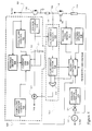
- a phase-controlled power modulation system 100 functionally comprises a switch assembly 102, a phase controller 104, a transition shaper 106, a switch protector 108 and an asymmetric waveform selector 110.
- the purpose of system 100 is to modulate the power from an AC source 112 delivered to a load 114.
- switch assembly 102 The function of switch assembly 102 is to alternative couple and decouple load 114 from AC source 112 to allow the power delivered to load 114 to be modulated.
- switch assembly 102 includes a pair of MOSFETs 116 and 118 in inverse series relationship. Since its body diode is forward biased only during a negative half cycle, MOSFET 116 controls power during positive half-cycles; similarly, MOSFET 118 has a body diode which is forward biased only during a positive half cycle, and thus controls power during negative half cycles of the AC waveform. Both switches can be held on when full power is required.
- switch assembly 102 can be operated in FPC mode, RPC mode and AHPC mode.
- FPC mode MOSFET 116 is off at the beginning of a positive half cycle, and is turned on at a time that the remaining AC waveform is calculated to provide the requested power.
- RPC mode MOSFET 116 is on at the beginning of a positive half cycle and is turned off when the requested RMS voltage has been achieved.
- AHPC mode MOSFET 116 starts on, turns off when a current limit is reached; MOSFET 116 turns on again during the same half cycle when the AC voltage falls sufficiently below that associated with the current limit.
- MOSFET 116 operates similarly during negative half cycles.
- MOSFETs 116 and 118 can be driven in alternation as taught in allowed U.S. Patent Application Serial Number 07/422,396 to Schanin. Independent switching is used to implement AHPC mode.
- tandem driving can be employed in all modes as taught by U.S. Patent No. 4,633,161 to Callahan et al. However, tandem operation is subject to zero-crossing detection errors.
- phase controller 104 The timing of the signals driving switch assembly 102 is generated by phase controller 104.
- Phase controller 104 has an input for receiving a requested RMS voltage.
- Phase controller 104 also monitors the switch output voltage. This permits a comparison of actual power to requested power so that power can be regulated.
- this regulation permits turn off time to be triggered when the requested power has been delivered on a cycle-by-cycle basis. This permits a constant power output despite significant variations in the AC waveform from source 112.
- FPC mode the regulation is on a delayed basis, so the regulation is somewhat less precise.
- Phase controller 104 is "asymmetric" in the sense that it only causes asymmetric waveforms to be delivered to load 114.
- FPC and RPC waveforms are inherently asymmetric.
- hybrid phase control waveforms can be symmetric as taught by Callahan et al.
- symmetric hybrid waveforms would not properly protect switch assembly 102.
- phase controller 104 is limited to generated asymmetric waveforms.
- the timing signals so generated trigger drive signals from transition shaper 106, which determines the shape of the transitions imposed by switch assembly 102.
- the drive signals determine the modulation of AC voltage during a switch transition.
- the transition shaper 106 limits the transition rate (dv/dt) to mimic the action of a magnetic choke in an SCR-type phase controller to minimize noise.
- the dv/dt ratio is not the only factor in dimmer noise.
- the rate of change of the voltage transition time, or dv 2 /dt 2 is a significant contributor to the noise generated by the lamp, as well as radiated and conducted electrical noise.
- Transition shaper 106 ensures a negative average second derivative in the transition drive signals to minimize sharp transitions, and thereby further minimize noise.
- transition shaper 106 provides for both a long mode and a short mode of operation.
- Switch protector 108 monitors current, voltage, and temperature to detect circuit threatening conditions. Voltage can be monitored to determine its amplitude in order to indicate an overvoltage and to determine its shape in order to detect excessive noise. In extreme and persistent conditions, switch protector 108 can trigger a decoupling of load 114 from source 112, by turning switch assembly 102 off.
- circuit-condition data from switch protector 108 is provided to asymmetric waveform selector 110 so it can trigger a waveform change to avert a shutdown, minimize the adverse consequences of a circuit-threatening condition, and/or minimize side effects of a response thereto by switch protector 108.
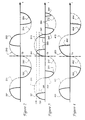
- asymmetric waveform selector 110 directs phase controller 104 to change from RPC mode to FPC mode, as indicated in FIG. 2.
- Four half cycles 201, 202, 203 and 204 of a load voltage are shown superimposed on four half cycles 211, 212, 213, and 214 of a source voltage.
- the first positive half cycle 201 and succeeding first negative half cycle 202 are shown in RPC mode.
- the second positive half cycle 203 and the second negative half cycle 204 occur after a waveform change around time T2 to FPC mode as indicated.
- asymmetric waveform selector 110 directs phase controller 104 to change from RPC mode to AHPC mode, as indicated in FIG. 3.
- Four half cycles 301, 302, 303 and 304 of a load voltage are shown superimposed on four half cycles 311, 312, 313, and 314 of a source voltage.
- the first positive half cycle 301 and succeeding first negative half cycle 302 are shown in RPC mode.
- the turn offs at 321 and 322 are forced since the current limit is reached.
- the load voltage waveform is changed around time T3 to AHPC mode.
- Second positive cycle 303 of the load voltage has a positive RPC component 341 and a positive FPC component 342.
- second negative cycle 304 has a RPC and FPC components 343 and 344.
- the turn on for positive FPC components 342 occurs as input cycle 313 drops below a confidence threshold 350 that is enough below current limit 330 to guarantee an overcurrent cannot reoccur during the present half cycle.
- the peak for FPC component 342 is necessarily below that of RPC component 341, rendering hybrid waveform 303 asymmetric.
- Hybrid waveform 304 is similarly asymmetric.
- asymmetric waveform selector 110 directs transition shaper 106 to change from long transition mode to short transition mode, as indicated in FIG. 4.
- load voltage half cycles 401, 402, 403 and 404 are shown superimposed on source voltage half cycles 411, 412, 413 and 414.
- the change of operational mode occurs around time T4.
- Half cycle 403 illustrates a shortened transition time. This half cycle is imposed on a copy 401' of first half cycle 401 to illustrate the change in transition time.
- Switch protector 108 also monitors instantaneous voltage during switch transitions, causing transition shaper 106 to instantaneously modify a drive signal to achieve the desired transition shape in the output power signal.
- FIGS. 5 and 6 The preferred embodiment of the present invention is described more structurally with reference to FIGS. 5 and 6.
- the correspondence of functional elements to structural elements is not one-to-one.
- multiple functions are performed by a single component.
- waveform selection and phase control are both primarily implemented by the same microcontroller.
- one function can be implemented by a combination of structural elements.
- the switch protector function utilizes a resistor to aid in detection of an overcurrent and a thermal sensor to aid in detection of overheating.
- phase-controlled power modulation system 100 The basic structure of phase-controlled power modulation system 100 is illustrated in FIG. 5.
- a diode D1 passes only the negative half-cycles of the voltage output from AC source 112.
- An analog-to-digital (A/D) convertor 504 converts the negative half cycle into a digital representation.
- a microcontroller 506 squares and integrates these half-wave digital representations of the analog input to compute its cumulative RMS voltage.
- the calculated cumulative RMS voltage is compared with a previously computed target RMS voltage that represents the power to be delivered from AC source 112 before VCS 102 is turned off (in RPC mode) or on (in FPC mode).
- the target value is calculated from a externally supplied requested RMS value.
- microcontroller 506 When the cumulative value is equal to the target value, microcontroller 506 provides a control signal to a transition controller 508 via an overcurrent detector 510. Transition controller 508 receives this control signal and switches the conductive state of MOSFET 116 off or on through control of its gate. MOSFET 116 is operated during the positive cycle in a mirror fashion by microcontroller 506, by its setting of a one-half cycle timer (of microcontroller 506) when the cumulative RMS voltages reaches the target RMS voltage during the negative cycle. A half-cycle period is 8.33 ms long in a 60 Hz system, and 10 ms long in a 50 Hz system. This timer will then expire at the same phase angle in the positive cycle as it does during the negative cycle, interrupting microcontroller 506 and causing it to change the state of MOSFET 116 as required by the operating mode of phase-controlled power modulation system 100.
- Microcontroller 506 controls the operational modes of system 100.
- System 100 normally operates in RPC mode, whereby MOSFET 116 is always enabled during the positive cycle when it will be reverse biased, so it can begin conduction when the negative cycle begins and it becomes forward biased.
- MOSFET 116 is only enabled at the target RMS voltage, and is turned off sometime during the positive cycle when it is reverse biased.
- microcontroller 506 controls system 100 to operate in AHPC mode during an overload or an incandescent lamp warm-up, as will be discussed in detail below.
- Overcurrent detector 510 is connected to the gates of MOSFETs 116 and 118 via transition controller 508. Overcurrent detector 510 is also coupled to a sense resistor R1 and microcontroller 506. When the voltage generated across sense resistor R1 exceeds a predetermined threshold value, overcurrent detector 510 overrides microcontroller 506 and causes transition controller 508 to switch off the forward biased MOSFET 116, thereby protecting it from damage due to overcurrent. Concurrently, overcurrent detector 510 signals microcontroller 506. If the current mode of operation is RPC, microcontroller 506 uses this signal to determine whether it should change to AHPC mode. If the overcurrent condition persists for a predetermined duration, e.g., several seconds, in AHPC or FPC mode, the system 100 can shut down temporarily and retry later, for example, five seconds later.
- a predetermined duration e.g., several seconds, in AHPC or FPC mode
- An inductive load sensing circuit 514 is connected between load 114 and microcontroller 506.
- load 114 is an inductive load and system 100 is operating in RPC mode
- voltage transients are generated back to MOSFET 118 and are detected by inductive load sensing circuit 514.
- inductive load sensing circuit 514 sends a signal to microcontroller 506 which debounces this input signal.
- a predetermined threshold of a consecutive number of inductive load signals is reached, the timing of the signals generated by microcontroller 506 to transition controller 508 is modified so that system 100 operates in FPC mode.
- transition controller 508 comprises two identical circuits, one for each respective MOSFET 116 and 118. Only the transition controller 508 for MOSFET 116 is illustrated in FIG. 5. Its counterpart is connected to node N1, at the gate of MOSFET 118. Transition controller 508 includes a voltage follower 518, a capacitor C1, a controlled current source 522, a dynamic current sink control 524, a feedback device 526, a current sink 528, and a short/long transition control 530.
- Current sink 528 is coupled to a node N2 to provide capacitor C1 with Current sink 528 is coupled to a node N2 to provide capacitor C1 with stable discharge voltage.
- Current sink 528 is always enabled, continually sinking current, and therefore always attempting to completely discharge capacitor C1. This ensures that MOSFET 116 is kept off during power-up initialization.
- microcontroller 506 determines that MOSFET 116 must begin conduction, it enables current source 522.
- Current source 522 is much stronger than current sink 528, and therefore the voltage across capacitor C1 rises.
- Voltage follower 518 ensures that the voltage across capacitor C1 is mirrored at the gate of MOSFET 116, which therefore becomes conductive when the voltage at its gate exceeds its turn-on threshold.
- current source 522 When microcontroller 506 determines that MOSFET 116 should become non-conductive, current source 522 is disabled. This allows current sink 528 to discharge capacitor C1, and, through voltage follower 518, drive the gate voltage of MOSFET 116 below its threshold, rendering it non-conductive. Note, therefore, that the simple control of current source 522 is all that is required to control the conductive state of MOSFET 116. Also note that a NOR gate 532, which by virtue of being driven by inverted logic, functions as an AND gate, allowing either microcontroller 506 or overcurrent detector 510 to turn-off current source 522, and therefore terminate conduction by MOSFET 116.
- current sink 528 is dynamically modified by feedback device 526 and dynamic current sink control 524, and is statically modified by short/long transition control 530.
- Dynamic current sink control 524 and feedback device 526 are coupled to node N3 to provide input to current sink 528 regarding voltage changes (feedback device 526) and the absolute voltage (current sink control 524) across MOSFET 116.
- the half-wave DC signal at node N3 is attenuated by dynamic current sink control 524 and is supplied at its output.
- Feedback device 526 provides a negative feedback signal that adjusts current sink 528 to sink substantially less current when MOSFET 116 enters its active region, so as to allow for the lengthy transition period.
- Dynamic current sink control 524 increases the current sunk by current sink 528 as the voltage rises across MOSFET 116. This ensures that the load voltage undergoes a very gradual transition as MOSFET 116 enters its active region. The gradual transition corresponds to a small dv 2 /dt 2 , minimizing noise.
- the voltage change during the fourth quarter duratic of a transition is at least twice that of the voltage change during the first quarter. This is made possible using a transition characterized by a negative average second derivative.
- the function of the short/long transition control 530 is to provide current sink 528 with two selectable base biases to allow it to operate in a long transition mode when thermal load is low, and a short transition mode when the thermal load is high.
- Overcurrent detector 510 includes a sensing section 534, a detection circuit 536 and NOR gate 532.
- Sensing section 534 is connected to node N4 to detect the voltage across sense resistor R1.
- the negative input of section 534 is asserted. Consequently, there is a output from detection circuit 536.
- the signal from detection circuit 536 is inverted by NOR gate 532.
- Current source 522 is thereby switched off by the signal from NOR gate 532 so that capacitor C1 begins its discharge cycle (since current sink 528 is always enabled). Accordingly, the voltage at node N2 decreases, transitioning MOSFET 116 to its non-conductive state.
- Thermal sensor 538 is in physical contact with switch assembly 102 to measure its temperature. Microcontroller monitors the output of thermal sensor 538 and compares this output to a predetermined warning threshold. When the warning threshold is exceeded, microcontroller 506 asserts a signal to short/long transition control 530 to effect a change from long to short transition mode. If thermal sensor 538 indicates that the temperature of switch assembly 102 continues to rise above a shutdown threshold, microcontroller 506 shuts switch assembly 102 off. Microcontroller 506 reenables switch assembly 102 once its temperature falls below the warning threshold.
- Voltage follower 518 includes a gate oscillation resistor R2, and transistors Q1 and Q2.
- Transistors Q2 and Q4 are configured as a voltage follower to mirror the voltage at node N2 to the gate of MOSFET 116.
- Gate oscillation resistor R2 prevents high frequency oscillations of MOSFET 116.
- Feedback device 526 includes a capacitor C2
- dynamic current sink control 524 includes a resistor R15
- short/long transition control 530 includes a NOR gate 602.
- Controlled-current source 522 includes transistors Q3, Q4 and Q5, and resistors R3, R4, R5 and R6.
- Current source transistor Q3 and current source resistor R3 are arranged to constitute a constant current source whose bias is established by current source bias resistors R4 and R5.
- Transistor Q4 is configured as a temperature compensating diode.
- Transistor Q5 is configured as a current source switch. Upon arrival of a high level signal from NOR gate 532, transistor Q5 is turned on so that constant current source 522, constituted by transistors Q3 and Q4, is turned on.
- Resistor R6 is a current limit resistor for NOR gate 532.
- Current sink 528 includes transistors Q6 and Q7 and resistors R7, R8, R9, and R10.
- Transistor Q6 and resistor R8 form a constant current sink whose bias is established by resistors R7, R9, R10, and resistor R15 which functions as dynamic current sink control 524.
- Transistor Q7 is configured as a temperature compensating diode for current sink 528.
- Capacitor C1 is therefore discharged via transistor Q6 and resistor R8.
- Capacitor C2 serves as a feedback mechanism that injects additional current into node N5 (at the emitter of transistor Q6) when the voltage at node N3 begins to change. This ensures that the discharge of capacitor C1 slows in the active region of MOSFET 116.
- the rising voltage at node N3 is attenuated by resistor R3 and increases the bias applied to the base of transistor Q6 and therefore the current sunk by transistor Q6. This technique allows a slow entry into the active region, with a faster exit from said region.
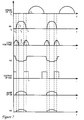
- the resulting voltage at node N4 can be seen in FIGURE 7 as a gradually sloping waveform with minimal dv 2 /dt 2 .
- the voltage at node N2 keeps MOSFET 116 operating in its active region so that the load voltage waveform is curved, as shown FIG. 7.
- Prior art circuits particularly those revealed in US Patent 4,540,893 to Bloomer, only provide sharp transitions that are shown by the straight line waveform S, superimposed on the load voltage in FIG. 7.
- the straight line waveform means a high dv 2 /dt 2 of the AC voltage in fall/rise transition time, which contributes to electrical noise.
- the resulting initial decrease in current sunk by current sink 528 due to feedback capacitor C2 is more than offset by the increase in the current sunk due to current source resistor R3, and therefore causes the same dv 2 /dt 2 elimination and waveform shaping that was described above.
- microcontroller 506 When the system is in AHPC mode, microcontroller 506 simply causes pairs of the above described transitions to occur.
- Sensing section 534 includes a transistor Q8, a diode D2, and resistors R11 and R12.
- the base of Q8 is grounded via resistor R12, which serves as a current-limit resistor.
- the collector of Q8 is coupled to diode D2 so that the DC bias applied to the collector of Q8 via pull-up resistor R11 is blocked from node N2 and capacitor C1 by diode D2.
- the emitter of Q8 is coupled to sense resistor R1 via node N4.
- a voltage comparator 604 and a flip-flop 606 constitute detection circuit 536.
- the voltage at node N4 becomes increasingly negative as the current through MOSFET 116 increases.
- V be of transistor Q8 When the voltage differential between ground and node N4 exceeds V be of transistor Q8, it conducts and attempts to discharge capacitor C1 through diode D2.
- the reference voltage of comparator 604 is V dd , the same voltage used by current source 522 to charge capacitor C1.
- sensing section 534 When transistor Q8 turns on, regardless of the charge on capacitor C1, its collector drops to a minimum level of V dd less two diode drops (one drop from Q3 and one from D2). If the overcurrent fault causes significant dv/dt, sensing section 534 also discharges node N2 at a rate faster than current sink 528 is normally capable of. This enhances the state change of MOSFET 116 from fully saturated to its active region and the start of the transition to a non-conductive state. The double diode drop assures that comparator 604 asserts its output low anytime transistor Q8 turns on; the low output resets flip-flop 606 so that its Q output goes high. NOR gate 532 therefore provides a low level output to Q5, turning it off and stopping capacitor C1 from charging. The constantly enabled current sink 528 thus starts the discharge cycle of capacitor C1.
- microcontroller 506 When required to turn MOSFET 116 on, microcontroller 506 asserts low the input to NOR gate 532 and the clock input CP of flip-flop 606. This forces its Q output to go low due to a high D input. The low level at output Q is NORed with the low level from microcontroller 506 at NOR gate 532, providing a high level signal to turn Q5 on.
- NOR gate 532 To turn MOSFET 116 off, a high level output from microcontroller 506 is applied to one input of NOR gate 532. Note that although this signal is also applied to clock input CP of flip-flop 606, it has no affect since flip-flop 606 is falling-edge triggered. The high level output is applied to the input of NOR gate 532, providing a low output that turns Q5 off.
- Inductive load sensing circuit 514 includes divider resistors R13 and R14, and a voltage comparator 608.
- the voltage across load 114 is applied to divider resistors R13 and R14, providing an attenuated voltage at the positive input of comparator 608.
- a reference voltage Vcc is applied to the negative input of comparator 608.
- microcontroller 506 counts the number of consecutive AC cycles that have outputs from comparator 608 until it reaches a predetermined count. Any one cycle without a signal resets the counter. If the predetermined count has been reached, microcontroller 506 modifies the timing of the signals it drives into overcurrent detector 510 to operate system 100 in FPC mode.
- Microcontroller 506 performs a real-time accumulated RMS voltage calculation using a step-wise square and integration.
- An integration target value is calculated from a requested RMS value input to microprocessor 506.
- the accumulated RMS voltage is repeatedly compared with the target value. When the target is reached, appropriate action based on the system's mode is taken, but the RMS calculation continues until no additional voltage is available for integration. This last step allows the recording of the RMS voltage available from AC source 112.
- the calculated integration target value differs from the requested RMS value to account for additional RMS accumulation during shut off, which is not instantaneous. Indeed, there are three types of delays that are encountered before the voltage at the load is reduced to zero: the transition period, additional hardware delays in the various elements, and software delays inherent in executing instructions and servicing interrupts. While the last two items are basically fixed delays, the energy delivered to the load as a function of them can vary based on the absolute voltage at transition time. While the amount of RMS voltage accumulated when the peak voltage is very low yields is small in absolute terms, it may be large when compared to the energy delivered to the load. The same holds true for delays that occur at high peak voltages. In addition, the energy contained in the transition period which occurs after the integration target has been reached, can also vary based on the peak voltage at the time of transition.
- a transition time correction table with different correction values C is stored in microcontroller 506. Different correction values can reflect differences waveform shape, transition times, and various hardware and software delays. When both the input voltage and the requested RMS voltage are determined, the correction value corresponding to the RMS value of the waveform can be obtained from the correction table.
- A/D converter 504 converts the output of the AC source 112 into digital signals.
- Microcontroller 506 further squares and integrates each digital sample during the negative half cycle. The resulting cumulative value is compared with the target value in microcontroller 506. If the target value has been reached, the drive signals to VCS 108 and 110 are complemented. Therefore, regardless of whether the system is in RPC or FPC mode, each MOSFET is correctly transitioned from one conductive state to the other.
- microcontroller 106 continues to monitor voltage to calculate the RMS voltage delivered to the load. If the RMS voltage calculated to this point is zero, this indicates that the AC voltage from AC power 112 has not yet transitioned to the negative half cycle, so monitoring and calculation continue.
- a timer interruption is scheduled for exactly one half cycle after the target is reached (8.33 Ms in a 60 Hz system, 10.0 Ms in a 50 Hz system) so that the MOSFET 116 has its state changed at exactly the same position in the positive cycle as MOSFET 118 had its state changed in the negative cycle.
- the integration process for the RMS voltage is resumed.
- the total voltage value applied to the load during one cycle of AC voltage is recorded by microcontroller 506.
- microcontroller 506 records the absolute voltage of the AC waveform at which the overload occurs, and calculates the voltage at which the MOSFET should be re-enabled. This re-enable voltage is a function of the overload voltage. The re-enable voltage must be lower than the overload voltage to avoid a second overload shutdown, since the lamp filament cools during the period of no conduction, and will therefore have a lower impedance and draw higher current at the voltage. In general, the lower the turn off voltage, the higher the differential must be between the overload voltage threshold and the re-enable voltage threshold.
- an asymmetric hybrid phase control mode provides for the required differential between the overload voltage threshold and the re-enable voltage threshold. Since no time base exists during the positive half cycle, a timer records the time period of non-conduction by the MOSFET (that is, until the re-enable voltage is reached).
- the present invention provides for many alternatives to the preferred embodiment described above. Different switch types are provided for.
- the primary operating mode can be RPC, FPC or an alternative mode. Power control applications other than dimming of lighting fixtures are provided for.
Description
Claims (22)
- A phase-controlled power modulation system for modulating the power delivered to a load (114) from an AC source (112), said system comprising:a switch assembly (102) for controlling the voltage across said load (114), said switch assembly (102) being between said load (114) and said AC source (112), said switch assembly (102) having at least two alternative conduction states;a transition shaper (106) for controlling the rate of change of voltage applied across said load (114) when said switch assembly (102) changes states, said transition shaper (106) being coupled to said switching assembly (102);a phase controller (104) for controlling said switch assembly (102) to implement phase control of said power, said phase controller (104) determining the timing of transitions of said switch assembly (102), said phase controller (104) being coupled to said transition shaper (106) for triggering switch transitions; anda switch protector (108) for protecting said switch assembly (102) in response to a circuit-threatening condition, said switch protector (108) including detector means (514,534,538) for detecting said circuit-threatening condition; characterised byan asymmetric waveform selector (110) for selecting between a normal operational mode characterised by a normal mode asymmetric waveform and a protective mode characterised by a protective mode asymmetric waveform, said protective mode asymmetric waveform being different from said normal mode asymmetric waveform, each protective waveform being shaped so that the power delivered through said switch assembly (102) during the first 90° AC half cycle is different from the power delivered through said switch assembly (102) during last 90° of the same AC half cycle, said asymmetric waveform selector (110) being coupled to said switch protector (108) for determining when to switch between said normal and protective modes, said asymmetric waveform selector (110) being coupled to said phase controller (104) and/or to said transition shaper (106) for implementing a selected mode.
- A phase-controlled power modulation system as recited in Claim 1 wherein said detector means (514) detects an overvoltage condition across said load (114), said asymmetric waveform selector (110) causing a mode change from a normal reverse phase control mode to a protective forward phase control mode in response to this detection.
- A phase-controlled power modulation system as recited in Claim 1 wherein said detector means (534) detects an overcurrent condition through said switch assembly (102), said switch protector (108) limiting the voltage across said load (114) in response to this detection, said asymmetric waveform selector (110) causing a mode change from a forward or reverse normal phase control mode to a protective asymmetric hybrid control mode in response to said detection.
- A phase-controlled power modulation system as recited in Claim 1 wherein said detector means (538) detects an excessive temperature around said switch assembly (102), said asymmetric waveform selector (110) causing said transition shaper (106) to change from a normal long transition time mode to a protective short transition time mode in response to said detection.
- A phase-controlled power modulation system as recited in Claim 1 wherein said transition controller (508) causing the transition time during a protective mode to be the same as the transition time during the immediately preceding period of normal operation.
- A phase-controlled power modulation system as recited in Claim 1 wherein said transition controller (508) effects a load-voltage transition profile with a negative average second derivative.
- A phase-controlled power modulation system as recited in Claim 6; characterised by said phase controller (104) driving said switch assembly (102) so that the RMS voltage delivered through said switch assembly (102) during any given quarter AC cycle is different from the RMS voltage delivered through said switch assembly (102) during the next quarter AC cycle, said phase controller (104) being coupled to said switch assembly (102) so as to effect said driving.
- A phase-controlled power modulation system as recited in Claim 7, said system comprising:a voltage limiter (514) for limiting said voltage in response to a circuit-threatening condition, said voltage limiter including detector means for detecting said circuit-threatening condition, said voltage limiter being coupled to said switch assembly (102) to effect limiting of said voltage.
- A phase-controlled power modulation system as recited in Claim 1, said system comprising:first and second voltage-controlled switches (116,118) for controlling the current flow through said load (114), said switches (116,118) being in inverse series connection between said load (114) and said AC source (112);analog-to-digital conversion means (504) for encoding an AC waveform, said analog-to-digital conversion means (504) coupling to said AC source (112) for receiving said AC waveform therefrom, said analog-to-digital conversion means (504) having a digital output at which it supplies a digital representation of said AC waveform;processing means (506) for calculating the RMS voltage to be delivered to said load (114) and for determining the operational mode of said voltage-controlled switches (116,118), said processing means (506) coupling to the output of said analog-to-digital conversion means (504) for squaring and integrating said digital representation to provide a calculated RMS voltage, said processing means (506) having a digital output at which it supplies a trigger signal when said calculated RMS voltage achieves a predetermined value; andtransition control means (508) for controlling operation of said voltage-controlled switches (116,118) in their respective active regions during a transition, said transition control means (508) having a trigger input, a voltage input and a switching control output, said trigger input coupling to said digital output of said processing means (506), said voltage input coupling to said AC source (112), and said switching control output coupling to said voltage-controlled switches (116,118), said transition control means (508) providing a transition control signal at said switching control output in response to said trigger signal, said transition control signal keeping each of said voltage-controlled switches (116,118) operating at its active region during said transition so that a load voltage waveform across said load is curved.
- A phase-controlled power modulation system as recited in Claim 9, wherein said transition means (508) includescontrolled current source means (522) for supplying a constant current, said controlled current source means (522) having a controlled input, said controlled input being coupled to said processing means (506) so that said state of controlled current source means (522) is changed by said trigger signal when the RMS voltage to be delivered to said load equals said predetermined value,a capacitance element (C1) for providing said transition control signal to said first voltage-controlled switch (116), said capacitance element (C1) being coupled to said controlled current source means (522) and said first voltage-controlled switch (116) so that said controlled current source means (522) charges said capacitance element (C1) while said controlled current source means (522) stays on,a voltage follower (518) for mirroring the voltage potential on said capacitance element (C1) to said first voltage-controlled switch (116),dynamic current sink control means (524) for providing a dynamic current, said dynamic current sink control means (524) having an input and an output, said input coupling tc said AC source (112), said dynamic current sink control means (524) providing said dynamic current at its output, said dynamic current being in phase with said AC signal,current sink means (528) for discharging said capacitance element (C1), said current sink means (528) having a dynamic current input, a feedback current input and a discharge port, said dynamic current input coupling to the output of said dynamic current control means (524) for receiving said dynamic current, said discharge port coupling to said capacitance element (C1), andfeedback means (526) for providing a feedback signal, said feedback means (526) having an input coupled to said AC,source (112) and said input of said dynamic current sink control means (524), said feedback device (526) having an output coupled to said current sink means (528) to provide a negative feedback signal that keeps the sink current flow through said current sink means (528) substantially constant, said dynamic current dynamically offsetting said current sink means (528) so that said current sink means (528) uniformly discharges said capacitance element (C1) in response to said feedback signal when said trigger signal turns off said controlled current source (522).
- A system as recited in Claim 10, wherein said transition control means (508) further comprises long/short transition control means (530), said long/short transition control means (530) having an input and an output, the input of said long/short transition control means (530) coupling to said processing means (506) so that when said first voltage-controlled switch (116) is thermally overloaded, said processing means (506) first determines in which operational mode said first voltage-controlled switch (116) is operating, and if said voltage-controlled switch (116) is operating in a reverse phase control mode, said processing means (506) causing said long/short transition control means (530) to send a signal that accelerates said current sink means (528) to discharge said capacitance element (C1) so that said first voltage-controlled switch (116) is turned off quickly, and if said first voltage-controlled switch (116) is operating in a phase control mode, said processing means (506) causing said long/short transition control means (530) to send a signal that blocks said current sink means (528) from discharging said capacitance element (C1) so that said first voltage-controlled switch (116) is turned on quickly.
- A system as recited in Claim 10, wherein said dynamic current sink control means (524) is a resistance element.
- A system as recited in Claim 10, wherein said short/long transition control means (530) is a resistance element.
- A system as recited in Claim 10, wherein said feedback device (526) is a capacitance element.
- A system as recited in Claim 10 comprising an overcurrent detection means (510) arranged between said processing means (506) and said transition control means (508), said overcurrent detection means (510) coupling to said voltage-controlled switches (116,118) via a sensing element (R1), said overcurrent detection means (510) coupling to said processing means (506) for providing a switching signal to said transition control means (508) when an overcurrent occurs, said switching signal turning said controlled current source (522) off so that said capacitance element (C1) is discharged by said current sink means (528).
- A system a recited in Claim 15, wherein said overcurrent detection means (520) comprises:a logic gate (532) for providing said switching signal, said switching signal being coupled to said controlled current source means (522) in response to said second logic output and said trigger signal from said processing means (506).sensing means (534) for detecting overcurrent, said sensing means (534) coupling to said sensing element (R1) to provide a sensing signal at its output when overcurrent occurs;detecting means (536) for comparing said sensing signal with a predetermined threshold and providing a comparison output when said sensing signal is higher than said predetermined threshold, said detecting means (536) havingcomparing means (604) for comparing said predetermined threshold with said sensing signal, said comparing means generating said comparison output when said sensing signal is over said predetermined threshold, andflip-flop means (606) for providing two complementary logic outputs, said flip-flop mean (606) generating a first logic output and a second logic output in response to said comparison output, said first logic output being applied to said processing means (506) to establish a phase control operational mode when overcurrent occurs; and
- A system as recited in Claim 10 further comprising an inductive sensing means (514), said inductive sensing means (514) providing a pulse output to said processing means (506) every time the voltage across said load (114) is over a reference potential, and when successive pulse outputs reach a predetermined number, said processing means (506) sending said trigger signal to switch the operational mode of said voltage-controlled switches (116,118) to a phase control operational mode.
- A system as recited in Claim 10 wherein in the warm-up period of said load (114), said processing means (506) turns said voltage-controlled switch (116,118) off at the moment that said AC voltage rises to an overcurrent-threatening voltage, and said processing means (506) turns said voltage-controlled switch (116,118) on again at the moment that said AC voltage falls to a predetermined value below said overcurrent-threatening voltage so that two power pulses are applied to said load during a half cycle of AC voltage.
- A phase-controlled power modulation system as recited in Claim 1 and for controlling the phase angle of current flow through a load (114) from an alternating current (AC) source (112), said system comprising:a pair of voltage-controlled switches (116,118) for controlling the current flow through said load (114), said switches (116,118) including a first voltage-controlled switch (116) and a second voltage-controlled switch (118) that are in inverse series connection between said load (114) and said AC source (112);an analog-to-digital (A/D) conversion means (504) for converting an AC signal into digital signals, said A/D conversion means (504) coupling to said AC source (112) and supplying digital output signals;processing means (506) for calculating the RMS voltage to be delivered to said load (114) and determining the operational mode of said voltage-controlled switches (116,118),said processing means (506) coupling to the output of said A/D conversion means (504) for calculating the root-mean-square (RMS) value of the digital output signals, said processing means (506) calculating said RMS value that is compared with a predetermined value, when said RMS value equals said predetermined value, said processing means (506) sending a control signal to turn said first voltage-controlled switch (116) off, said processing means (506) calculating a turn-off phase angle of said second voltage-controlled switch (118) on the basis of the turn-off phase angle of said first voltage-controlled switch (116),said processing means (506) monitoring thermal overload of said voltage-controlled switches (116,118), and when thermal overload occurs, said processing means (506) providing said control signal to quickly transition said voltage-controlled switches (116,118) so that the thermal overload is moderated;overcurrent detection means (510) for detecting overcurrent, said overcurrent detection means (510) coupling to said processing means (506), and when overcurrent occurs or said overcurrent detection means (510) receives said control signal from said processing means (506), said overcurrent detection means (510) sending a trigger signal; andtransition control means (508) for controlling said voltage-controlled switches (116,118) to operate at their respective active regions during a transition so that the voltage waveform applied to said load (114) is curved to reduce noise, said transition control means (508) havingcontrolled current source means (522) for supplying a stable current, said controlled current source means (522) having a controlled input, said controlled input coupling to said overcurrent detection means (510) to receive said trigger signal that determines the operational mode of said controlled current source means (522),a capacitance element (C1) for providing said transition control signal to said first voltage-controlled switch (116), said capacitance element (C1) coupling to said controlled current source means (522) and the gate of said first voltage-controlled switch (116), said capacitance element (C1) being charged by said controlled current source means (522),a voltage follower (518) for mirroring the voltage potential on said capacitance element (C1) to the gate of said first voltage-controlled switch (116),dynamic current sink control means (524) for providing a dynamic output current, said dynamic current sink control means (524) having an input and an output, said input coupling to said AC source (112), said dynamic current sink control means (524) providing such dynamic output current at its output,a feedback device (526) for providing a feedback signal, said feedback device (526) having an input coupled to said AC source (112) and the input of said dynamic current sink control means (524), said feedback device (526) having an output for providing a negative feedback signal that causes a sink current to remain substantially constant,current sink means (528) for discharging said capacitance element (C1), said current sink means (528) having a dynamic current input, a feedback current input and a discharge port, said dynamic current input coupling to the output of said dynamic current control means (524), said feedback current input coupling to the output of said feedback device (526), said discharge port coupling to said capacitance element (C1), said dynamic current dynamically offsetting said current sink means (528) so that said current sink means (528) uniformly discharges said capacitance element (C1) in response to said feedback signal while said controlled current source means (522) stays off, andlong/short transition control means (530) for controlling the sink current of said current sink means (528), said long/short transition control means (530) having an input and an output, said input coupling to said processing means (506),when said first voltage-controlled switch (116) produces thermal overload, said processing means (506) provides a signal to said long/short transition control means (530) to change the sink current,when said first voltage-controlled switch (116) is operating during a fall transition of reverse phase control operational mode, the output signal of said processing means (506) causes said long/short transition control means (530) to send a signal that accelerates said current sink means (528) to discharge said capacitance element (C1) so that said first voltage-controlled switch (116) is turned off quickly, andwhen said first voltage-controlled switch (116) is operating during a rise transition of phase control operational mode, said processing means (506) causes said long/short transition control means (530) to send a signal that blocks said current sink means (528) from discharging said capacitance element (C1) so that said first voltage-controlled switch (116) is turned on quickly.
- A system as recited in Claim 19 wnerein when said load (114) operates during a warm-up period, said processing means (506)turns off said first voltage-controlled switch (116) at the time AC voltage across said first voltage-controlled switch (116) rises to an overcurrent-threatening voltage,turns on said first voltage-controlled switch (116), at the time AC voltage falls below said overcurrent-threatening voltage in a first half cycle,records the phase angles at which said first voltage-controlled switch (116) is turned off and on, andswitches on said second voltage-controlled switch (118) during the second half cycle as a function of the recorded phase angles.
- A system as recited in Claim 19 further comprising an inductive sensing means (514), said inductive sensing means (514) having its detection input coupled to said load (114), said inductive sensing means (514) providing a pulse output to said processing means (506) when it detects an inductor, said processing means (506) sending said control signal to said controlled current source means (522) to keep said voltage-controlled switches (116,118) operating in a forward phase control (FPC) mode.
- A system as recited in Claim 19, wherein said processing means (506) transitions said voltage-controlled switches (116,118) in a first cycle, measures the total RMS value of said first cycle, and calculates the transition phase angle of said first voltage-controlled switch (116) and second voltage-controlled switch (118) so that said first and second voltage-controlled switches (116,118) are respectively transitioned at said calculated transition phase angle in a second cycle.
Applications Claiming Priority (3)
| Application Number | Priority Date | Filing Date | Title |
|---|---|---|---|
| US07/659,101 US5239255A (en) | 1991-02-20 | 1991-02-20 | Phase-controlled power modulation system |
| PCT/US1992/001253 WO1992015052A1 (en) | 1991-02-20 | 1992-02-18 | Phase-controlled power modulation system |
| US659101 | 2000-09-11 |
Publications (3)
| Publication Number | Publication Date |
|---|---|
| EP0572567A1 EP0572567A1 (en) | 1993-12-08 |
| EP0572567A4 EP0572567A4 (en) | 1994-04-13 |
| EP0572567B1 true EP0572567B1 (en) | 1998-07-22 |
Family
ID=24644029
Family Applications (1)
| Application Number | Title | Priority Date | Filing Date |
|---|---|---|---|
| EP92908447A Expired - Lifetime EP0572567B1 (en) | 1991-02-20 | 1992-02-18 | Phase-controlled power modulation system |
Country Status (5)
| Country | Link |
|---|---|
| US (1) | US5239255A (en) |
| EP (1) | EP0572567B1 (en) |
| CN (1) | CN1068237A (en) |
| TW (1) | TW205115B (en) |
| WO (1) | WO1992015052A1 (en) |
Families Citing this family (99)
| Publication number | Priority date | Publication date | Assignee | Title |
|---|---|---|---|---|
| US5629607A (en) * | 1984-08-15 | 1997-05-13 | Callahan; Michael | Initializing controlled transition light dimmers |
| US5225765A (en) * | 1984-08-15 | 1993-07-06 | Michael Callahan | Inductorless controlled transition and other light dimmers |
| US5329223A (en) * | 1992-06-26 | 1994-07-12 | Green Technologies, Inc. | Ideal voltage controller for conserving energy in inductive loads |
| US5444359A (en) * | 1992-06-26 | 1995-08-22 | Green Technologies, Inc. | Load sensitive variable voltage motor controller |
| DE4231060A1 (en) * | 1992-09-17 | 1994-03-24 | Abb Patent Gmbh | Electronic dimming method and dimmer for carrying out the method |
| DE4310723A1 (en) * | 1993-04-01 | 1994-10-06 | Abb Patent Gmbh | Method for controlling the alternating current in a load circuit and device for carrying out the method |
| US5693995A (en) | 1993-06-14 | 1997-12-02 | Ecoair Corp. | Hybrid alternator |
| US5506480A (en) * | 1993-11-12 | 1996-04-09 | Entertainment Technology, Inc. | Paired dimmers for controlling harmonic currents |
| US5847555A (en) * | 1995-08-01 | 1998-12-08 | Lewis; Dennis E. | Source voltage sensitive load controller |
| US5600233A (en) * | 1995-08-22 | 1997-02-04 | Chicago Stage Equipment Co. | Electronic power control circuit |
| CA2168941A1 (en) * | 1996-02-06 | 1997-08-07 | Barna Szabados | Dimmer for fluorescent lighting |
| US6215633B1 (en) | 1996-02-26 | 2001-04-10 | Marconi Communications, Inc. | Active current limiter |
| FR2767017B1 (en) * | 1997-07-31 | 1999-10-15 | Sgs Thomson Microelectronics | CALL CURRENT LIMITING CIRCUIT |
| DE19738857A1 (en) * | 1997-09-05 | 1999-04-15 | Abb Patent Gmbh | Dimmer system |
| DE19754866A1 (en) * | 1997-12-10 | 1999-06-17 | Siemens Ag | Universal dimmer and method for dimming |
| FR2786331B1 (en) * | 1998-11-24 | 2001-02-02 | Legrand Sa | ELECTRONIC PROTECTION AGAINST SHORT-CIRCUITS |
| AT410604B (en) * | 1999-03-02 | 2003-06-25 | Legrand Oesterreich | CONTROL DEVICE FOR CONTROLLING THE CURRENT FLOW ANGLE |
| US6218785B1 (en) * | 1999-03-19 | 2001-04-17 | Incerti & Simonini Di Incerti Edda & C. S.N.C. | Low-tension lighting device |
| FR2802360B1 (en) * | 1999-12-14 | 2002-03-01 | Legrand Sa | METHOD AND DEVICE FOR ELECTRIC POWER SUPPLY OF A LOAD BY A DRIVE HAS AT LEAST ONE SWITCH CONTROLLED |
| WO2001067589A1 (en) | 2000-03-09 | 2001-09-13 | Ecoair Corp. | Alternator system |
| EP1336326A4 (en) * | 2000-11-22 | 2004-04-14 | Fusion Uv Sys Inc | Ultraviolet lamp power supply and method for operating at high power/reduced cooling using cycling |
| DE10113690A1 (en) * | 2001-03-21 | 2002-10-02 | Eltako Gmbh Schaltgeraete | dimmer |
| US6969959B2 (en) * | 2001-07-06 | 2005-11-29 | Lutron Electronics Co., Inc. | Electronic control systems and methods |
| US6667868B2 (en) * | 2001-10-03 | 2003-12-23 | Maxim Integrated Products, Inc. | Thermal shutdown control for multi-channel integrated circuit boards |
| FR2830379B1 (en) * | 2001-10-03 | 2004-08-06 | Agence Spatiale Europeenne | DEVICE FOR PROTECTING A VOLTAGE SOURCE AND A LOAD SUPPLIED BY THE VOLTAGE SOURCE |
| DE10156686A1 (en) * | 2001-11-17 | 2003-05-28 | Merten Gmbh & Co Kg | Dimmer with load type detection |
| US6798627B2 (en) | 2002-02-05 | 2004-09-28 | Onan Corporation | Engine generator set systems and methods providing load power fault protection |
| FR2846484B1 (en) * | 2002-10-24 | 2005-01-14 | Legrand Sa | METHOD AND APPARATUS FOR CONTROLLING THE AVERAGE POWER SUPPLY POWER OF AN ALTERNATING CURRENT LOAD |
| FR2856236B1 (en) * | 2003-06-16 | 2005-08-05 | Hager Electro Sas | METHOD AND DEVICE FOR SELF-ADAPTING A VARIATOR TO A LOAD |
| TWI249287B (en) * | 2003-06-25 | 2006-02-11 | Matsushita Electric Works Ltd | Electronic switch |
| US6967852B2 (en) | 2003-12-19 | 2005-11-22 | Silent Power, Inc. | Power converter with dynamic current limiting |
| US20050162870A1 (en) * | 2004-01-23 | 2005-07-28 | Hirst B. M. | Power converter |
| US8253394B2 (en) * | 2004-02-17 | 2012-08-28 | Hewlett-Packard Development Company, L.P. | Snubber circuit |
| US7259524B2 (en) * | 2004-06-10 | 2007-08-21 | Lutron Electronics Co., Inc. | Apparatus and methods for regulating delivery of electrical energy |
| US7977919B1 (en) | 2005-04-06 | 2011-07-12 | Rf Micro Devices, Inc. | Over-voltage protection accounting for battery droop |
| US7190124B2 (en) * | 2005-05-16 | 2007-03-13 | Lutron Electronics Co., Inc. | Two-wire dimmer with power supply and load protection circuit in the event of switch failure |
| US7382595B2 (en) * | 2005-05-25 | 2008-06-03 | Electronic Theatre Controls, Inc. | Low voltage overcurrent protection for solid state switching system |
| DE602005022634D1 (en) * | 2005-08-10 | 2010-09-09 | Energetix Voltage Control Ltd | VOLTAGE REGULATOR DEVICE |
| JP4701052B2 (en) * | 2005-09-21 | 2011-06-15 | 矢崎総業株式会社 | Overcurrent detection device |
| WO2007042598A1 (en) * | 2005-10-11 | 2007-04-19 | Schneider Electric Industries Sas | Improved power regulator automatically setting forward or reverse phase control depending on the type of load |
| CN101405923B (en) * | 2005-12-12 | 2012-07-04 | 澳大利亚奇胜有限公司 | Load detector for a dimmer |
| TW200738068A (en) | 2005-12-12 | 2007-10-01 | Clipsal Australia Pty Ltd | A universal dimmer |
| US7394203B2 (en) * | 2005-12-15 | 2008-07-01 | Monolithic Power Systems, Inc. | Method and system for open lamp protection |
| US7463469B2 (en) * | 2006-02-02 | 2008-12-09 | Texas Instruments Incorporated | System and method for current overload response with class D topology |
| US7619365B2 (en) * | 2006-04-10 | 2009-11-17 | Lutron Electronics Co., Inc. | Load control device having a variable drive circuit |
| US7962109B1 (en) * | 2007-02-27 | 2011-06-14 | Rf Micro Devices, Inc. | Excess current and saturation detection and correction in a power amplifier |
| US7956615B1 (en) | 2007-02-27 | 2011-06-07 | Rf Micro Devices, Inc. | Utilizing computed battery resistance as a battery-life indicator in a mobile terminal |
| EP1965283B1 (en) * | 2007-02-27 | 2010-07-28 | STMicroelectronics Srl | Improved voltage regulator with leakage current compensation |
| US20080246414A1 (en) * | 2007-04-05 | 2008-10-09 | Jian Xu | Inductive load sensor for dimmer circuit |
| US7855518B2 (en) * | 2007-06-19 | 2010-12-21 | Masco Corporation | Dimming algorithms based upon light bulb type |
| DE102007036438B4 (en) * | 2007-08-02 | 2010-09-23 | Abb Ag | Method for controlling a universal dimmer |
| US8085009B2 (en) * | 2007-08-13 | 2011-12-27 | The Powerwise Group, Inc. | IGBT/FET-based energy savings device for reducing a predetermined amount of voltage using pulse width modulation |
| US8619443B2 (en) | 2010-09-29 | 2013-12-31 | The Powerwise Group, Inc. | System and method to boost voltage |
| US8085010B2 (en) * | 2007-08-24 | 2011-12-27 | The Powerwise Group, Inc. | TRIAC/SCR-based energy savings device for reducing a predetermined amount of voltage using pulse width modulation |
| US8120307B2 (en) * | 2007-08-24 | 2012-02-21 | The Powerwise Group, Inc. | System and method for providing constant loading in AC power applications |
| US8698447B2 (en) | 2007-09-14 | 2014-04-15 | The Powerwise Group, Inc. | Energy saving system and method for devices with rotating or reciprocating masses |
| US8810190B2 (en) | 2007-09-14 | 2014-08-19 | The Powerwise Group, Inc. | Motor controller system and method for maximizing energy savings |
| WO2009036516A1 (en) | 2007-09-19 | 2009-03-26 | Clipsal Australia Pty Ltd | Dimmer circuit with overcurrent detection |
| US7868561B2 (en) | 2007-10-31 | 2011-01-11 | Lutron Electronics Co., Inc. | Two-wire dimmer circuit for a screw-in compact fluorescent lamp |
| ES2365553T3 (en) * | 2007-12-03 | 2011-10-06 | Sirio Panel S.P.A. | CIRCUIT CONFIGURATION TO GENERATE A MODULATED SIGNAL IN PULSE WIDTH, TO OPERATE ELECTRICAL CHARGES. |
| US8058852B2 (en) * | 2008-04-23 | 2011-11-15 | Woongjin Coway Co., Ltd. | Device and method for detecting zero crossing and voltage amplitude from single pulse signal |
| US8004255B2 (en) | 2008-08-07 | 2011-08-23 | The Powerwise Group, Inc. | Power supply for IGBT/FET drivers |
| DE102008045234B4 (en) * | 2008-08-29 | 2013-11-07 | Esw Gmbh | Method and arrangement for harmonic suppression in AC-powered air heaters with PTC technology |
| US8710812B1 (en) * | 2009-01-27 | 2014-04-29 | Xilinx, Inc. | Regulating a supply voltage provided to a load circuit |
| US8350416B2 (en) * | 2009-06-30 | 2013-01-08 | Schanin David J | Transition-rate control for phase-controlled AC power delivery system |
| US8208235B2 (en) * | 2009-09-04 | 2012-06-26 | Lutron Electronics Co., Inc. | Method of detecting a fault condition of a load control device |
| US8698446B2 (en) | 2009-09-08 | 2014-04-15 | The Powerwise Group, Inc. | Method to save energy for devices with rotating or reciprocating masses |
| EA021950B1 (en) | 2009-09-08 | 2015-10-30 | Дзе Пауэрвайз Груп, Инк. | Energy saving system and method for devices with rotating or reciprocating masses |
| US8698408B2 (en) | 2009-11-25 | 2014-04-15 | Lutron Electronics Co., Inc. | Two-wire dimmer switch for low-power loads |
| US8664881B2 (en) | 2009-11-25 | 2014-03-04 | Lutron Electronics Co., Inc. | Two-wire dimmer switch for low-power loads |
| US8957662B2 (en) | 2009-11-25 | 2015-02-17 | Lutron Electronics Co., Inc. | Load control device for high-efficiency loads |
| US8988050B2 (en) | 2009-11-25 | 2015-03-24 | Lutron Electronics Co., Inc. | Load control device for high-efficiency loads |
| US8729814B2 (en) * | 2009-11-25 | 2014-05-20 | Lutron Electronics Co., Inc. | Two-wire analog FET-based dimmer switch |
| US9160224B2 (en) | 2009-11-25 | 2015-10-13 | Lutron Electronics Co., Inc. | Load control device for high-efficiency loads |
| US11870334B2 (en) | 2009-11-25 | 2024-01-09 | Lutron Technology Company Llc | Load control device for high-efficiency loads |
| JP5431193B2 (en) * | 2010-02-10 | 2014-03-05 | Tone株式会社 | Electric tool |
| DE102010048980A1 (en) | 2010-04-19 | 2011-10-20 | Permundo Gmbh | Control device and method for detecting a type of load |
| JP5501851B2 (en) * | 2010-05-12 | 2014-05-28 | Tone株式会社 | Phase control device |
| CA2799631A1 (en) * | 2010-05-17 | 2011-11-24 | Koninklijke Philips Electronics N.V. | Method and apparatus for detecting and correcting improper dimmer operation |
| DE102010024128A1 (en) * | 2010-06-17 | 2011-12-22 | Diehl Ako Stiftung & Co. Kg | Alternating voltage regulators |
| EP2402834B1 (en) * | 2010-06-25 | 2013-08-21 | Yuieh Hsene Electronics Co., Ltd. | Alternating current regulating means |
| US8193787B2 (en) * | 2010-07-06 | 2012-06-05 | V Square/R, LLC | System and method for regulating RMS voltage delivered to a load |
| US9279835B2 (en) * | 2012-01-25 | 2016-03-08 | Control4 Corporation | Device for detecting a load type |
| CN104322151B (en) * | 2012-03-28 | 2016-06-29 | 卢特龙电子公司 | Method and apparatus for phase controlling load |
| US9578692B2 (en) | 2012-04-19 | 2017-02-21 | Infineon Technologies Americas Corp. | Power converter with tank circuit and over-voltage protection |
| US10340692B2 (en) | 2012-04-19 | 2019-07-02 | Pass & Seymour, Inc. | Universal power control device |
| CN102780403A (en) * | 2012-08-22 | 2012-11-14 | 杭州龙科电子有限公司 | Single-phase trailing edge chopper voltage regulator |
| US9084324B2 (en) | 2013-02-26 | 2015-07-14 | Lutron Electronics Co., Inc. | Load control device having automatic setup for controlling capacitive and inductive loads |
| JP6496471B2 (en) * | 2013-02-28 | 2019-04-03 | 日立オートモティブシステムズ株式会社 | Load drive control device |
| WO2015109357A1 (en) * | 2014-01-24 | 2015-07-30 | Hendon Semiconductors Pty Ltd | Phase cutting controlled dimmer arrangement with over-current protection when powering a lamp |
| US9961727B2 (en) * | 2014-05-22 | 2018-05-01 | Ozuno Holdings Limited | Phase control dimmer circuit |
| CN104066261B (en) * | 2014-06-16 | 2017-03-15 | 广州斯全德灯光有限公司 | Sine wave dimming method and sinusoidal dimmer under overcurrent protection mechanism |
| DE102015214631B3 (en) * | 2015-07-31 | 2016-11-03 | Siemens Schweiz Ag | Dimming device and method for power control of a lighting device |
| US10187944B2 (en) | 2015-09-04 | 2019-01-22 | Lutron Electronics Co., Inc. | Load control device for high-efficiency loads |
| US9882492B2 (en) * | 2015-12-08 | 2018-01-30 | Infineon Technologies Austria Ag | Control of asymmetric parallel synchronous rectifiers in power converter topologies |
| EP4203616A1 (en) | 2017-06-09 | 2023-06-28 | Lutron Technology Company LLC | Load control device having an overcurrent protection circuit |
| US10714925B2 (en) | 2017-10-10 | 2020-07-14 | Littelfuse, Inc. | Self-powered electronic fuse with storage capacitor that charges with minimal disturbance of load current through the fuse |
| WO2020236659A1 (en) * | 2019-05-17 | 2020-11-26 | Lutron Technology Company Llc | Load control device having a closed-loop gate drive circuit |
| US10568185B1 (en) | 2019-07-18 | 2020-02-18 | Leviton Manufacturing Company, Inc. | Two-wire dimmer operation |
Family Cites Families (11)
| Publication number | Priority date | Publication date | Assignee | Title |
|---|---|---|---|---|
| US4540893A (en) * | 1983-05-31 | 1985-09-10 | General Electric Company | Controlled switching of non-regenerative power semiconductors |
| US4528494A (en) * | 1983-09-06 | 1985-07-09 | General Electric Company | Reverse-phase-control power switching circuit and method |
| US4567425A (en) * | 1983-12-14 | 1986-01-28 | General Electric Company | Method of and apparatus for half-cycle-average or R.M.S. load voltage control |
| US4633161A (en) * | 1984-08-15 | 1986-12-30 | Michael Callahan | Improved inductorless phase control dimmer power stage with semiconductor controlled voltage rise time |
| US4823069A (en) * | 1984-08-15 | 1989-04-18 | Michael Callahan | Light dimmer for distributed use employing inductorless controlled transition phase control power stage |
| US4617508A (en) * | 1984-11-02 | 1986-10-14 | General Electric Company | Reverse phase-control apparatus for multiplexing interconnections between power switching and control circuit modules |
| US4688161A (en) * | 1986-07-16 | 1987-08-18 | Vari-Lite, Inc. | Regulated power supply apparatus and method using reverse phase angle control |
| US5038081A (en) * | 1987-12-16 | 1991-08-06 | Lutron Electronics Co., Inc. | Reverse phase-controlled dimmer |
| DK13489A (en) * | 1988-03-30 | 1989-10-01 | Insta Elektro Gmbh & Co Kg | BRIGHTNESS REGULATION CIRCUIT FOR INCIDENTAL LIGHTS AND NETWORK PARTS WITH A PROTECTIVE AND LIMIT CIRCUIT TO GET AN ELECTRONIC SECURITY |
| US5004969A (en) * | 1989-10-16 | 1991-04-02 | Bayview Technology Group, Inc. | Phase control switching circuit without zero crossing detection |
| US5072170A (en) * | 1990-08-06 | 1991-12-10 | Watlow Controls | Reverse phase angle control of A.C. power loads |
-
1991
- 1991-02-20 US US07/659,101 patent/US5239255A/en not_active Expired - Lifetime
-
1992
- 1992-02-18 EP EP92908447A patent/EP0572567B1/en not_active Expired - Lifetime
- 1992-02-18 WO PCT/US1992/001253 patent/WO1992015052A1/en active IP Right Grant
- 1992-02-20 CN CN92101627A patent/CN1068237A/en active Pending
- 1992-04-23 TW TW081103199A patent/TW205115B/zh active
Also Published As
| Publication number | Publication date |
|---|---|
| TW205115B (en) | 1993-05-01 |
| US5239255A (en) | 1993-08-24 |
| EP0572567A1 (en) | 1993-12-08 |
| CN1068237A (en) | 1993-01-20 |
| WO1992015052A1 (en) | 1992-09-03 |
| EP0572567A4 (en) | 1994-04-13 |
Similar Documents
| Publication | Publication Date | Title |
|---|---|---|
| EP0572567B1 (en) | Phase-controlled power modulation system | |
| EP0191838B1 (en) | A dimmer power stage | |
| AU2002346046B2 (en) | Electronic control systems and methods | |
| US9496691B2 (en) | Universal load control module | |
| US7271550B2 (en) | Dimmer circuit arrangement | |
| US20020079849A1 (en) | AC power converter | |
| CA2425587C (en) | Reverse phase control power switching circuit with overload protection | |
| AU2002346046A1 (en) | Electronic control systems and methods | |
| JPS6373870A (en) | Power control system | |
| EP1782662A2 (en) | Controllable power supply circuit for an illumination system and methods of operation thereof | |
| US5994883A (en) | Alternating current power control device | |
| JP4951069B2 (en) | Power controller with current limited RMS voltage regulated output | |
| US9332613B2 (en) | Current limiter with active damping | |
| US5463307A (en) | High efficiency, low voltage adapter apparatus and method | |
| JP3536933B2 (en) | Incandescent dimmer | |
| JP4069482B2 (en) | Light control device | |
| JP3928133B2 (en) | Incandescent light dimmer | |
| AU2008201337A1 (en) | Electronic control systems and methods | |
| GB2297441A (en) | Power controller | |
| Charreton | Soft Light Dimmer | |
| JP2003229294A (en) | Phase control device |
Legal Events
| Date | Code | Title | Description |
|---|---|---|---|
| PUAI | Public reference made under article 153(3) epc to a published international application that has entered the european phase |
Free format text: ORIGINAL CODE: 0009012 |
|
| 17P | Request for examination filed |
Effective date: 19930914 |
|
| AK | Designated contracting states |
Kind code of ref document: A1 Designated state(s): GB |
|
| A4 | Supplementary search report drawn up and despatched |
Effective date: 19940222 |
|
| AK | Designated contracting states |
Kind code of ref document: A4 Designated state(s): GB |
|
| 17Q | First examination report despatched |
Effective date: 19960530 |
|
| GRAG | Despatch of communication of intention to grant |
Free format text: ORIGINAL CODE: EPIDOS AGRA |
|
| GRAG | Despatch of communication of intention to grant |
Free format text: ORIGINAL CODE: EPIDOS AGRA |
|
| GRAH | Despatch of communication of intention to grant a patent |
Free format text: ORIGINAL CODE: EPIDOS IGRA |
|
| GRAH | Despatch of communication of intention to grant a patent |
Free format text: ORIGINAL CODE: EPIDOS IGRA |
|
| GRAA | (expected) grant |
Free format text: ORIGINAL CODE: 0009210 |
|
| AK | Designated contracting states |
Kind code of ref document: B1 Designated state(s): GB |
|
| PG25 | Lapsed in a contracting state [announced via postgrant information from national office to epo] |
Ref country code: GB Free format text: LAPSE BECAUSE OF NON-PAYMENT OF DUE FEES Effective date: 19990218 |
|
| PLBE | No opposition filed within time limit |
Free format text: ORIGINAL CODE: 0009261 |
|
| STAA | Information on the status of an ep patent application or granted ep patent |
Free format text: STATUS: NO OPPOSITION FILED WITHIN TIME LIMIT |
|
| 26N | No opposition filed | ||
| GBPC | Gb: european patent ceased through non-payment of renewal fee |
Effective date: 19990218 |