EP0572230A2 - Piezoelectric/electrostrictive actuator having integral ceramic base member and film-type piezoelectric/electrostrictive element(s) - Google Patents
Piezoelectric/electrostrictive actuator having integral ceramic base member and film-type piezoelectric/electrostrictive element(s) Download PDFInfo
- Publication number
- EP0572230A2 EP0572230A2 EP93304069A EP93304069A EP0572230A2 EP 0572230 A2 EP0572230 A2 EP 0572230A2 EP 93304069 A EP93304069 A EP 93304069A EP 93304069 A EP93304069 A EP 93304069A EP 0572230 A2 EP0572230 A2 EP 0572230A2
- Authority
- EP
- European Patent Office
- Prior art keywords
- piezoelectric
- electrostrictive
- plate
- base member
- ink
- Prior art date
- Legal status (The legal status is an assumption and is not a legal conclusion. Google has not performed a legal analysis and makes no representation as to the accuracy of the status listed.)
- Granted
Links
- 239000000919 ceramic Substances 0.000 title claims abstract description 43
- 125000006850 spacer group Chemical group 0.000 claims abstract description 22
- 238000000034 method Methods 0.000 claims abstract description 13
- 230000008859 change Effects 0.000 claims abstract description 4
- 238000004891 communication Methods 0.000 claims description 20
- MCMNRKCIXSYSNV-UHFFFAOYSA-N Zirconium dioxide Chemical compound O=[Zr]=O MCMNRKCIXSYSNV-UHFFFAOYSA-N 0.000 claims description 18
- 239000013078 crystal Substances 0.000 claims description 7
- SIWVEOZUMHYXCS-UHFFFAOYSA-N oxo(oxoyttriooxy)yttrium Chemical compound O=[Y]O[Y]=O SIWVEOZUMHYXCS-UHFFFAOYSA-N 0.000 claims description 5
- 229910010293 ceramic material Inorganic materials 0.000 claims description 4
- 229910002077 partially stabilized zirconia Inorganic materials 0.000 claims description 3
- 239000002245 particle Substances 0.000 claims description 3
- PNEYBMLMFCGWSK-UHFFFAOYSA-N aluminium oxide Inorganic materials [O-2].[O-2].[O-2].[Al+3].[Al+3] PNEYBMLMFCGWSK-UHFFFAOYSA-N 0.000 claims description 2
- 229910002078 fully stabilized zirconia Inorganic materials 0.000 claims 1
- 239000000463 material Substances 0.000 description 17
- 239000000853 adhesive Substances 0.000 description 11
- 230000001070 adhesive effect Effects 0.000 description 11
- 239000010408 film Substances 0.000 description 9
- 150000001875 compounds Chemical class 0.000 description 6
- 239000000758 substrate Substances 0.000 description 6
- 238000006073 displacement reaction Methods 0.000 description 5
- 229910052751 metal Inorganic materials 0.000 description 5
- 239000002184 metal Substances 0.000 description 5
- PXHVJJICTQNCMI-UHFFFAOYSA-N Nickel Chemical compound [Ni] PXHVJJICTQNCMI-UHFFFAOYSA-N 0.000 description 4
- 238000010304 firing Methods 0.000 description 4
- 230000008569 process Effects 0.000 description 4
- 230000002829 reductive effect Effects 0.000 description 4
- 229910045601 alloy Inorganic materials 0.000 description 3
- 239000000956 alloy Substances 0.000 description 3
- RKTYLMNFRDHKIL-UHFFFAOYSA-N copper;5,10,15,20-tetraphenylporphyrin-22,24-diide Chemical compound [Cu+2].C1=CC(C(=C2C=CC([N-]2)=C(C=2C=CC=CC=2)C=2C=CC(N=2)=C(C=2C=CC=CC=2)C2=CC=C3[N-]2)C=2C=CC=CC=2)=NC1=C3C1=CC=CC=C1 RKTYLMNFRDHKIL-UHFFFAOYSA-N 0.000 description 3
- 230000000694 effects Effects 0.000 description 3
- 238000007641 inkjet printing Methods 0.000 description 3
- 238000004519 manufacturing process Methods 0.000 description 3
- 230000002441 reversible effect Effects 0.000 description 3
- XEEYBQQBJWHFJM-UHFFFAOYSA-N Iron Chemical compound [Fe] XEEYBQQBJWHFJM-UHFFFAOYSA-N 0.000 description 2
- KDLHZDBZIXYQEI-UHFFFAOYSA-N Palladium Chemical compound [Pd] KDLHZDBZIXYQEI-UHFFFAOYSA-N 0.000 description 2
- 229910001252 Pd alloy Inorganic materials 0.000 description 2
- 229910052787 antimony Inorganic materials 0.000 description 2
- 230000015572 biosynthetic process Effects 0.000 description 2
- BRPQOXSCLDDYGP-UHFFFAOYSA-N calcium oxide Chemical compound [O-2].[Ca+2] BRPQOXSCLDDYGP-UHFFFAOYSA-N 0.000 description 2
- 239000000292 calcium oxide Substances 0.000 description 2
- ODINCKMPIJJUCX-UHFFFAOYSA-N calcium oxide Inorganic materials [Ca]=O ODINCKMPIJJUCX-UHFFFAOYSA-N 0.000 description 2
- 229910000420 cerium oxide Inorganic materials 0.000 description 2
- 238000010276 construction Methods 0.000 description 2
- 238000003475 lamination Methods 0.000 description 2
- 229910052451 lead zirconate titanate Inorganic materials 0.000 description 2
- 238000003754 machining Methods 0.000 description 2
- 239000000395 magnesium oxide Substances 0.000 description 2
- CPLXHLVBOLITMK-UHFFFAOYSA-N magnesium oxide Inorganic materials [Mg]=O CPLXHLVBOLITMK-UHFFFAOYSA-N 0.000 description 2
- AXZKOIWUVFPNLO-UHFFFAOYSA-N magnesium;oxygen(2-) Chemical compound [O-2].[Mg+2] AXZKOIWUVFPNLO-UHFFFAOYSA-N 0.000 description 2
- 239000000203 mixture Substances 0.000 description 2
- 229910052759 nickel Inorganic materials 0.000 description 2
- BMMGVYCKOGBVEV-UHFFFAOYSA-N oxo(oxoceriooxy)cerium Chemical compound [Ce]=O.O=[Ce]=O BMMGVYCKOGBVEV-UHFFFAOYSA-N 0.000 description 2
- 238000005192 partition Methods 0.000 description 2
- BASFCYQUMIYNBI-UHFFFAOYSA-N platinum Chemical compound [Pt] BASFCYQUMIYNBI-UHFFFAOYSA-N 0.000 description 2
- 230000010287 polarization Effects 0.000 description 2
- 239000002243 precursor Substances 0.000 description 2
- 238000007789 sealing Methods 0.000 description 2
- 229910052684 Cerium Inorganic materials 0.000 description 1
- VYZAMTAEIAYCRO-UHFFFAOYSA-N Chromium Chemical compound [Cr] VYZAMTAEIAYCRO-UHFFFAOYSA-N 0.000 description 1
- PWHULOQIROXLJO-UHFFFAOYSA-N Manganese Chemical compound [Mn] PWHULOQIROXLJO-UHFFFAOYSA-N 0.000 description 1
- 229910001260 Pt alloy Inorganic materials 0.000 description 1
- HCHKCACWOHOZIP-UHFFFAOYSA-N Zinc Chemical compound [Zn] HCHKCACWOHOZIP-UHFFFAOYSA-N 0.000 description 1
- IHWJXGQYRBHUIF-UHFFFAOYSA-N [Ag].[Pt] Chemical compound [Ag].[Pt] IHWJXGQYRBHUIF-UHFFFAOYSA-N 0.000 description 1
- 230000002159 abnormal effect Effects 0.000 description 1
- 239000000654 additive Substances 0.000 description 1
- 230000000996 additive effect Effects 0.000 description 1
- WATWJIUSRGPENY-UHFFFAOYSA-N antimony atom Chemical compound [Sb] WATWJIUSRGPENY-UHFFFAOYSA-N 0.000 description 1
- 229910052788 barium Inorganic materials 0.000 description 1
- DSAJWYNOEDNPEQ-UHFFFAOYSA-N barium atom Chemical compound [Ba] DSAJWYNOEDNPEQ-UHFFFAOYSA-N 0.000 description 1
- 239000011230 binding agent Substances 0.000 description 1
- -1 cadnium Chemical compound 0.000 description 1
- ZMIGMASIKSOYAM-UHFFFAOYSA-N cerium Chemical compound [Ce][Ce][Ce][Ce][Ce][Ce][Ce][Ce][Ce][Ce][Ce][Ce][Ce][Ce][Ce][Ce][Ce][Ce][Ce][Ce][Ce][Ce][Ce][Ce][Ce][Ce][Ce][Ce][Ce][Ce][Ce][Ce][Ce][Ce][Ce][Ce][Ce][Ce] ZMIGMASIKSOYAM-UHFFFAOYSA-N 0.000 description 1
- 229910052804 chromium Inorganic materials 0.000 description 1
- 239000011651 chromium Substances 0.000 description 1
- 239000011248 coating agent Substances 0.000 description 1
- 238000000576 coating method Methods 0.000 description 1
- 229910017052 cobalt Inorganic materials 0.000 description 1
- 239000010941 cobalt Substances 0.000 description 1
- GUTLYIVDDKVIGB-UHFFFAOYSA-N cobalt atom Chemical compound [Co] GUTLYIVDDKVIGB-UHFFFAOYSA-N 0.000 description 1
- 239000004020 conductor Substances 0.000 description 1
- 239000002178 crystalline material Substances 0.000 description 1
- 238000005520 cutting process Methods 0.000 description 1
- 230000002950 deficient Effects 0.000 description 1
- NKZSPGSOXYXWQA-UHFFFAOYSA-N dioxido(oxo)titanium;lead(2+) Chemical compound [Pb+2].[O-][Ti]([O-])=O NKZSPGSOXYXWQA-UHFFFAOYSA-N 0.000 description 1
- 238000007598 dipping method Methods 0.000 description 1
- 239000007772 electrode material Substances 0.000 description 1
- 239000003822 epoxy resin Substances 0.000 description 1
- 229910002112 ferroelectric ceramic material Inorganic materials 0.000 description 1
- 239000012530 fluid Substances 0.000 description 1
- 239000011521 glass Substances 0.000 description 1
- 238000010438 heat treatment Methods 0.000 description 1
- 230000002401 inhibitory effect Effects 0.000 description 1
- 238000009413 insulation Methods 0.000 description 1
- 238000007733 ion plating Methods 0.000 description 1
- 238000010884 ion-beam technique Methods 0.000 description 1
- 229910052742 iron Inorganic materials 0.000 description 1
- 229910052746 lanthanum Inorganic materials 0.000 description 1
- FZLIPJUXYLNCLC-UHFFFAOYSA-N lanthanum atom Chemical compound [La] FZLIPJUXYLNCLC-UHFFFAOYSA-N 0.000 description 1
- HEPLMSKRHVKCAQ-UHFFFAOYSA-N lead nickel Chemical compound [Ni].[Pb] HEPLMSKRHVKCAQ-UHFFFAOYSA-N 0.000 description 1
- JQJCSZOEVBFDKO-UHFFFAOYSA-N lead zinc Chemical compound [Zn].[Pb] JQJCSZOEVBFDKO-UHFFFAOYSA-N 0.000 description 1
- HFGPZNIAWCZYJU-UHFFFAOYSA-N lead zirconate titanate Chemical compound [O-2].[O-2].[O-2].[O-2].[O-2].[Ti+4].[Zr+4].[Pb+2] HFGPZNIAWCZYJU-UHFFFAOYSA-N 0.000 description 1
- 239000007788 liquid Substances 0.000 description 1
- 229910052748 manganese Inorganic materials 0.000 description 1
- 239000011572 manganese Substances 0.000 description 1
- WPBNNNQJVZRUHP-UHFFFAOYSA-L manganese(2+);methyl n-[[2-(methoxycarbonylcarbamothioylamino)phenyl]carbamothioyl]carbamate;n-[2-(sulfidocarbothioylamino)ethyl]carbamodithioate Chemical compound [Mn+2].[S-]C(=S)NCCNC([S-])=S.COC(=O)NC(=S)NC1=CC=CC=C1NC(=S)NC(=O)OC WPBNNNQJVZRUHP-UHFFFAOYSA-L 0.000 description 1
- 230000008018 melting Effects 0.000 description 1
- 238000002844 melting Methods 0.000 description 1
- 150000002739 metals Chemical class 0.000 description 1
- 230000004048 modification Effects 0.000 description 1
- 238000012986 modification Methods 0.000 description 1
- 229910052758 niobium Inorganic materials 0.000 description 1
- 239000010955 niobium Substances 0.000 description 1
- GUCVJGMIXFAOAE-UHFFFAOYSA-N niobium atom Chemical compound [Nb] GUCVJGMIXFAOAE-UHFFFAOYSA-N 0.000 description 1
- 229910000510 noble metal Inorganic materials 0.000 description 1
- 230000001590 oxidative effect Effects 0.000 description 1
- ZBSCCQXBYNSKPV-UHFFFAOYSA-N oxolead;oxomagnesium;2,4,5-trioxa-1$l^{5},3$l^{5}-diniobabicyclo[1.1.1]pentane 1,3-dioxide Chemical compound [Mg]=O.[Pb]=O.[Pb]=O.[Pb]=O.O1[Nb]2(=O)O[Nb]1(=O)O2 ZBSCCQXBYNSKPV-UHFFFAOYSA-N 0.000 description 1
- 229910052763 palladium Inorganic materials 0.000 description 1
- SWELZOZIOHGSPA-UHFFFAOYSA-N palladium silver Chemical compound [Pd].[Ag] SWELZOZIOHGSPA-UHFFFAOYSA-N 0.000 description 1
- 230000036961 partial effect Effects 0.000 description 1
- 239000004033 plastic Substances 0.000 description 1
- 238000007747 plating Methods 0.000 description 1
- 229910052697 platinum Inorganic materials 0.000 description 1
- 229920000647 polyepoxide Polymers 0.000 description 1
- 238000007639 printing Methods 0.000 description 1
- 238000004080 punching Methods 0.000 description 1
- 229920005989 resin Polymers 0.000 description 1
- 239000011347 resin Substances 0.000 description 1
- 230000004044 response Effects 0.000 description 1
- 229910052703 rhodium Inorganic materials 0.000 description 1
- 239000010948 rhodium Substances 0.000 description 1
- MHOVAHRLVXNVSD-UHFFFAOYSA-N rhodium atom Chemical compound [Rh] MHOVAHRLVXNVSD-UHFFFAOYSA-N 0.000 description 1
- 238000007650 screen-printing Methods 0.000 description 1
- 239000004065 semiconductor Substances 0.000 description 1
- 239000002002 slurry Substances 0.000 description 1
- 239000002904 solvent Substances 0.000 description 1
- 238000005507 spraying Methods 0.000 description 1
- 238000004544 sputter deposition Methods 0.000 description 1
- 229910002076 stabilized zirconia Inorganic materials 0.000 description 1
- 230000000087 stabilizing effect Effects 0.000 description 1
- 239000010935 stainless steel Substances 0.000 description 1
- 229910001220 stainless steel Inorganic materials 0.000 description 1
- 229940071182 stannate Drugs 0.000 description 1
- 229910052712 strontium Inorganic materials 0.000 description 1
- CIOAGBVUUVVLOB-UHFFFAOYSA-N strontium atom Chemical compound [Sr] CIOAGBVUUVVLOB-UHFFFAOYSA-N 0.000 description 1
- 229920003002 synthetic resin Polymers 0.000 description 1
- 239000000057 synthetic resin Substances 0.000 description 1
- 229910052715 tantalum Inorganic materials 0.000 description 1
- GUVRBAGPIYLISA-UHFFFAOYSA-N tantalum atom Chemical compound [Ta] GUVRBAGPIYLISA-UHFFFAOYSA-N 0.000 description 1
- 239000010409 thin film Substances 0.000 description 1
- 230000009466 transformation Effects 0.000 description 1
- 238000000844 transformation Methods 0.000 description 1
- WFKWXMTUELFFGS-UHFFFAOYSA-N tungsten Chemical compound [W] WFKWXMTUELFFGS-UHFFFAOYSA-N 0.000 description 1
- 229910052721 tungsten Inorganic materials 0.000 description 1
- 239000010937 tungsten Substances 0.000 description 1
- 238000007740 vapor deposition Methods 0.000 description 1
- 229910052727 yttrium Inorganic materials 0.000 description 1
- VWQVUPCCIRVNHF-UHFFFAOYSA-N yttrium atom Chemical compound [Y] VWQVUPCCIRVNHF-UHFFFAOYSA-N 0.000 description 1
- 229910052725 zinc Inorganic materials 0.000 description 1
- 239000011701 zinc Substances 0.000 description 1
Images


Classifications
-
- B—PERFORMING OPERATIONS; TRANSPORTING
- B41—PRINTING; LINING MACHINES; TYPEWRITERS; STAMPS
- B41J—TYPEWRITERS; SELECTIVE PRINTING MECHANISMS, i.e. MECHANISMS PRINTING OTHERWISE THAN FROM A FORME; CORRECTION OF TYPOGRAPHICAL ERRORS
- B41J2/00—Typewriters or selective printing mechanisms characterised by the printing or marking process for which they are designed
- B41J2/005—Typewriters or selective printing mechanisms characterised by the printing or marking process for which they are designed characterised by bringing liquid or particles selectively into contact with a printing material
- B41J2/01—Ink jet
- B41J2/135—Nozzles
- B41J2/16—Production of nozzles
- B41J2/1621—Manufacturing processes
- B41J2/1623—Manufacturing processes bonding and adhesion
-
- B—PERFORMING OPERATIONS; TRANSPORTING
- B41—PRINTING; LINING MACHINES; TYPEWRITERS; STAMPS
- B41J—TYPEWRITERS; SELECTIVE PRINTING MECHANISMS, i.e. MECHANISMS PRINTING OTHERWISE THAN FROM A FORME; CORRECTION OF TYPOGRAPHICAL ERRORS
- B41J2/00—Typewriters or selective printing mechanisms characterised by the printing or marking process for which they are designed
- B41J2/005—Typewriters or selective printing mechanisms characterised by the printing or marking process for which they are designed characterised by bringing liquid or particles selectively into contact with a printing material
- B41J2/01—Ink jet
- B41J2/135—Nozzles
- B41J2/14—Structure thereof only for on-demand ink jet heads
- B41J2/14201—Structure of print heads with piezoelectric elements
- B41J2/14233—Structure of print heads with piezoelectric elements of film type, deformed by bending and disposed on a diaphragm
-
- B—PERFORMING OPERATIONS; TRANSPORTING
- B41—PRINTING; LINING MACHINES; TYPEWRITERS; STAMPS
- B41J—TYPEWRITERS; SELECTIVE PRINTING MECHANISMS, i.e. MECHANISMS PRINTING OTHERWISE THAN FROM A FORME; CORRECTION OF TYPOGRAPHICAL ERRORS
- B41J2/00—Typewriters or selective printing mechanisms characterised by the printing or marking process for which they are designed
- B41J2/005—Typewriters or selective printing mechanisms characterised by the printing or marking process for which they are designed characterised by bringing liquid or particles selectively into contact with a printing material
- B41J2/01—Ink jet
- B41J2/135—Nozzles
- B41J2/16—Production of nozzles
- B41J2/1607—Production of print heads with piezoelectric elements
- B41J2/161—Production of print heads with piezoelectric elements of film type, deformed by bending and disposed on a diaphragm
-
- B—PERFORMING OPERATIONS; TRANSPORTING
- B41—PRINTING; LINING MACHINES; TYPEWRITERS; STAMPS
- B41J—TYPEWRITERS; SELECTIVE PRINTING MECHANISMS, i.e. MECHANISMS PRINTING OTHERWISE THAN FROM A FORME; CORRECTION OF TYPOGRAPHICAL ERRORS
- B41J2/00—Typewriters or selective printing mechanisms characterised by the printing or marking process for which they are designed
- B41J2/005—Typewriters or selective printing mechanisms characterised by the printing or marking process for which they are designed characterised by bringing liquid or particles selectively into contact with a printing material
- B41J2/01—Ink jet
- B41J2/135—Nozzles
- B41J2/16—Production of nozzles
- B41J2/1621—Manufacturing processes
- B41J2/1632—Manufacturing processes machining
-
- B—PERFORMING OPERATIONS; TRANSPORTING
- B41—PRINTING; LINING MACHINES; TYPEWRITERS; STAMPS
- B41J—TYPEWRITERS; SELECTIVE PRINTING MECHANISMS, i.e. MECHANISMS PRINTING OTHERWISE THAN FROM A FORME; CORRECTION OF TYPOGRAPHICAL ERRORS
- B41J2/00—Typewriters or selective printing mechanisms characterised by the printing or marking process for which they are designed
- B41J2/005—Typewriters or selective printing mechanisms characterised by the printing or marking process for which they are designed characterised by bringing liquid or particles selectively into contact with a printing material
- B41J2/01—Ink jet
- B41J2/135—Nozzles
- B41J2/16—Production of nozzles
- B41J2/1621—Manufacturing processes
- B41J2/164—Manufacturing processes thin film formation
- B41J2/1642—Manufacturing processes thin film formation thin film formation by CVD [chemical vapor deposition]
-
- B—PERFORMING OPERATIONS; TRANSPORTING
- B41—PRINTING; LINING MACHINES; TYPEWRITERS; STAMPS
- B41J—TYPEWRITERS; SELECTIVE PRINTING MECHANISMS, i.e. MECHANISMS PRINTING OTHERWISE THAN FROM A FORME; CORRECTION OF TYPOGRAPHICAL ERRORS
- B41J2/00—Typewriters or selective printing mechanisms characterised by the printing or marking process for which they are designed
- B41J2/005—Typewriters or selective printing mechanisms characterised by the printing or marking process for which they are designed characterised by bringing liquid or particles selectively into contact with a printing material
- B41J2/01—Ink jet
- B41J2/135—Nozzles
- B41J2/16—Production of nozzles
- B41J2/1621—Manufacturing processes
- B41J2/164—Manufacturing processes thin film formation
- B41J2/1643—Manufacturing processes thin film formation thin film formation by plating
-
- B—PERFORMING OPERATIONS; TRANSPORTING
- B41—PRINTING; LINING MACHINES; TYPEWRITERS; STAMPS
- B41J—TYPEWRITERS; SELECTIVE PRINTING MECHANISMS, i.e. MECHANISMS PRINTING OTHERWISE THAN FROM A FORME; CORRECTION OF TYPOGRAPHICAL ERRORS
- B41J2/00—Typewriters or selective printing mechanisms characterised by the printing or marking process for which they are designed
- B41J2/005—Typewriters or selective printing mechanisms characterised by the printing or marking process for which they are designed characterised by bringing liquid or particles selectively into contact with a printing material
- B41J2/01—Ink jet
- B41J2/135—Nozzles
- B41J2/16—Production of nozzles
- B41J2/1621—Manufacturing processes
- B41J2/164—Manufacturing processes thin film formation
- B41J2/1646—Manufacturing processes thin film formation thin film formation by sputtering
-
- H—ELECTRICITY
- H10—SEMICONDUCTOR DEVICES; ELECTRIC SOLID-STATE DEVICES NOT OTHERWISE PROVIDED FOR
- H10N—ELECTRIC SOLID-STATE DEVICES NOT OTHERWISE PROVIDED FOR
- H10N30/00—Piezoelectric or electrostrictive devices
- H10N30/1051—Piezoelectric or electrostrictive devices based on piezoelectric or electrostrictive films or coatings
- H10N30/10513—Piezoelectric or electrostrictive devices based on piezoelectric or electrostrictive films or coatings characterised by the underlying bases, e.g. substrates
-
- H—ELECTRICITY
- H10—SEMICONDUCTOR DEVICES; ELECTRIC SOLID-STATE DEVICES NOT OTHERWISE PROVIDED FOR
- H10N—ELECTRIC SOLID-STATE DEVICES NOT OTHERWISE PROVIDED FOR
- H10N30/00—Piezoelectric or electrostrictive devices
- H10N30/20—Piezoelectric or electrostrictive devices with electrical input and mechanical output, e.g. functioning as actuators or vibrators
- H10N30/204—Piezoelectric or electrostrictive devices with electrical input and mechanical output, e.g. functioning as actuators or vibrators using bending displacement, e.g. unimorph, bimorph or multimorph cantilever or membrane benders
- H10N30/2047—Membrane type
-
- B—PERFORMING OPERATIONS; TRANSPORTING
- B41—PRINTING; LINING MACHINES; TYPEWRITERS; STAMPS
- B41J—TYPEWRITERS; SELECTIVE PRINTING MECHANISMS, i.e. MECHANISMS PRINTING OTHERWISE THAN FROM A FORME; CORRECTION OF TYPOGRAPHICAL ERRORS
- B41J2/00—Typewriters or selective printing mechanisms characterised by the printing or marking process for which they are designed
- B41J2/005—Typewriters or selective printing mechanisms characterised by the printing or marking process for which they are designed characterised by bringing liquid or particles selectively into contact with a printing material
- B41J2/01—Ink jet
- B41J2/135—Nozzles
- B41J2/14—Structure thereof only for on-demand ink jet heads
- B41J2002/14387—Front shooter
Definitions
- the present invention relates in general to a piezoelectric/electrostrictive actuator, and more particularly to such a piezoelectric/electrostrictive actuator which has a novel structure that assures improved and stable operating characteristics, and which can be produced with significantly improved efficiency.
- an actuator having a base member defining a pressure chamber, and a piezoelectric/electrostrictive element disposed on a wall of the pressure chamber, for raising the pressure of a fluid in the chamber so as to change the volume of the chamber.
- a piezoelectric/electrostrictive actuator may be used as an ink pump for a print head used in an ink jet printer, for example.
- an ink material is supplied to the pressure chambertofill the same, and the pressure within the chamber is raised by displacement of the piezoelectric/electrostrictive element, so that ink particles are jetted through a nozzle which communicates with the pressure chamber.
- FIGs. 5 and 6 there is illustrated an example of ink jet print head which uses as an ink pump the above-described piezoelectric/electrostrictive actuator.
- This print head has an ink nozzle member 16 which consists of a metallic nozzle plate 4 having a plurality of nozzles 2, a metallic orifice plate 8 having a plurality of orifices 6, and a channel plate 10, which are superposed on each other such that the channel plate 10 is interposed between the plates 4, 8.
- a piezoelectric/electrostrictive actuator 25 used as an ink pump forthe print head includes a base member 24 consisting of two plates 18, 20 made of metal or synthetic resin and formed in lamination on the ink nozzle member 16.
- the base member 24 is formed with a plurality of voids 22 which correspond to the nozzles 2 and orifices 6.
- a plurality of piezoelectric/electrostrictive elements 28 corresponding to the respective voids 22 are secured to an outer surface of the plate 18 of the base member 24 of the actuator 25. With this actuator 25 superposed on and bonded to the ink nozzle member 16, each of the voids 22 provides an ink chamber 26 in which the pressure of the ink is raised by displacement of the corresponding piezoelectric/electrostrictive element 28.
- an adhesive used for bonding the ink nozzle member 16 and the actuator25 is likely to overflow onto the opposite surfaces of the partition wall 30. Therefore, the ink chambers 26 and/or ink flow channels including the ink supply and discharge channels 12, 14 and orifices 6 may be deformed, whereby the ink-jetting characteristics of the print head may deteriorate, resulting in reduced quality and yield of the products (print heads).
- the ink nozzle member 16 and actuator 25 are insufficiently or poorly bonded together at some portions of the interface of the members 16,24. This may result in incomplete sealing between the adjacent ink chambers 26, 26, causing leakage of the pressures of the ink chambers 26, 26 and consequent crosstalk, for example.
- the partial or insufficient bonding may also leave gaps between the bonding surfaces of the members 16, 24, resulting in pressure loss upon pressurizing of the ink chambers 26 due to the air remaining in the gaps. Consequently, the ink-jetting characteristics of the print head may be lowered.
- a piezoelectric/electrostrictive actuator comprising: a ceramic base member in which at least one pressure chamber is formed, the ceramic base member comprising at least a spacer plate having at least one window which provides the pressure chamber or chambers, a closure plate disposed on one of opposite major surfaces of the spacer plate, for closing one opening of each window, and a connecting plate disposed on the other major surface of the spacer plate, for closing the other opening of each window, the connecting plate having at least one hole formed in alignment with the window(s), the spacer plate, the closure plate and the connecting plate being formed from respective ceramic green sheets which are laminated on each other and fired into an integral ceramic structure as the ceramic base member; and at least one piezoelectric/electrostrictive element each disposed on a wall partially defining the corresponding pressure chamber, for deforming the wall so as to change a pressure of the corresponding pressure chamber, each piezoelectric/ electrostrictive element comprising a piezoelectric/ electrostrictive unit consisting of
- the above piezoelectric/electrostrictive actuator constructed according to the present invention can be produced with significantly improved efficiency, assuring improved product quality, since two or more piezoelectric/ electrostrictive elements can be easily formed at a time by a film-forming method with high efficiency. This also makes the resultant actuator sufficiently small-sized. Since the ceramic base member has a three-layer structure consisting of the closure plate, the spacer plate and the connecting plate, the present actuator exhibits a sufficiently high degree of rigidity even before firing, i,e, even when it is a laminar structure of green sheets forthese plates, thereby assuring improved handling ease of the laminar structure and enhanced production efficiency of the actuator.
- the piezoelectric/electrostrictive actuator as described above may be suitably used as an ink pump for an ink jet print head, for example.
- the actuator having the above three-layer structure of the ceramic base member can be bonded to a member, such as an ink nozzle member of the print head, assuring a remarkably improved seal at bonding surfaces of the actuator and ink nozzle member so as to establish fluid-tightness of an ink flow channel through which the inkfiows through the print head.
- the thus obtained inkjet print head has an improved and stable product quality.
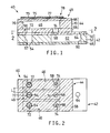
- FIG. 1 and 2 schematically showing an inkjet print head 40
- Fig. 3 which is an exploded perspective view of the print head 40
- an ink nozzle member 42 and a piezoelectric/electrostrictive actuator 45 as one embodiment of the present invention are bonded together to form an integral structure of the ink jet print head 40.
- an ink material is supplied to a plurality of pressure chambers 46 formed in the actuator 45, and is jetted or discharged from a plurality of nozzles 54 formed through the ink nozzle member 42.
- the ink nozzle member 42 consists of a nozzle plate 48 and an orifice plate 50 having a relatively small thickness, and a channel plate 52 interposed between these plates 48, 50.
- the nozzle plate 48 and the orifice plate 50 are integrally bonded to the channel plate 52 by means of an adhesive.
- the nozzle plate 48 has a plurality of nozzles 54 (three in this embodiment) formed therethrough, for permitting jets of fine ink particles, while the orifice plate 50 and the channel plate 52 have respective through-holes 56, 57 formed through the thicknesses thereof. These through-holes 56, 57 are aligned with the respective nozzles 54 as viewed in the direction of the thickness of the plates 48, 50, 52, and have a diameter which is larger by a given value than that of the nozzles 54.
- the orifice plate 50 further has a plurality of orifices 58 (three in this embodiment) formed therethrough, for permitting flow of the ink into to the respective pressure chambers 46.
- the channel plate 52 is formed with a window 60 which is closed at its opposite openings by the nozzle plate 48 and orifice plate 50, respectively, whereby an ink supply channel 62 communicating with the orifices 58 is defined by the channel plate 52, the nozzle plate 48 and the orifice plate 50.
- the orifice plate 50 further has a supply port 64 through which the ink is fed from an ink reservoir into the ink supply channel 62.
- each of the orifices 58 is desirably formed in tapered shape such that the diameter of the orifice 58 is reduced in the direction of flow of the ink (i.e., the direction from the ink supply channel 62 toward the pressure chambers 46), as shown in Fig. 1 by way of example, so as to function as a check valve for inhibiting the ink from flowing in the reverse direction.
- the piezoelectric/electrostrictive actuator 45 consists of a ceramic base member 44 and a plurality of piezoelectric/electrostrictive elements 78 formed integrally on the base member 44.
- the ceramic base member 44 consists of a closure plate 66 and a connecting plate 68 having a relatively small thickness, and a spacer plate 70 interposed between these plates 66, 68. These plates 66, 68, 70 are superposed on each other and formed integrally into the ceramic base member 44 in a manner as described later.
- the connecting plate 68 has first communication holes 72 and second communication holes 74 formed therethrough, which are respectively aligned with the through-holes 56 and orifices 58 formed in the orifice plate 50, as viewed in the direction of thickness of the plates 68,50.
- the diameter of the first communication holes 72 is substantially equal to or sl ig htly larger than that of the through-holes 56, while the diameter of the second communication holes 74 is larger by a given value than that of the orifices 58.
- the spacer plate 70 has a plurality of rectangular windows 76 formed therethrough.
- the spacer plate 70 is superposed on the connecting plate 68 such that each of the windows 76 communicates with the corresponding first and second communication holes 72, 74 formed in the connecting plate 68.
- the above-indicated closure plate 66 is superposed on one of the opposite major surfaces of the spacer plate 70 remote from the connecting plate 68, so as to close openings of the windows 76.
- the pressure chambers 46 are formed within the ceramic base member 44, such that the chambers 46 communicate with an exterior space through the first and second communication holes 72,74.
- the ceramic base member 44 is formed as an integrally formed fired ceramic structure. That is, in the process of producing the base member 44, green sheets are initially formed by using a slurry that is prepared from ceramic materials, binders, liquid solvents and others, by means of a generally used device such as a doctor blade device or a reverse roll coater. Then, the green sheets are subjected to suitable processing such as cutting, machining or punching, as needed, so as to form the windows 76 and the first and second communication holes 72, 74. Thus, there are formed precursors for the plates 66, 68, 70. These precursors are then laminated on each other and fired into an integral ceramic body as the ceramic base member 44.
- the closure plate 66 preferably has a thickness of 50 ⁇ m or smaller, more preferably, within a range of about 3 to 12wm.
- the connecting plate 68 preferably has a thickness of 10 ⁇ m or larger, more preferably, 50 ⁇ m or larger.
- the spacer plate 70 preferably has a thickness of 50 ⁇ m or larger, more preferably, 100 ⁇ m or larger.
- the above-described ceramic base member 44 which is formed as an integral fired ceramic structure, does not require any particular adhesive treatment for bonding the plates 66, 68, 70 together. Accordingly, complete and secure sealing can be achieved at the interfaces between the closure plate 66 and spacer plate 70 and between the connecting plate 68 and spacer plate 70.
- the ceramic base member 44 can be produced with improved efficiency, due to the presence of the connecting plate 68.
- the laminar structure including the connecting plate 68 exhibits an enhanced rigidity due to the presence of the plate 68, assuring improved handling ease thereof, while reducing the possibility of occurrence of defectives due to handling failure, as compared with when the structure does not include the connecting plate 68.
- the connecting plate 68 makes it possible to handle the laminar structure even in the above-described situation.
- the surface of the ceramic base member 44 which is to be bonded to the ink nozzle member 42, that is, the outer surface of the connecting plate 68, is made even or smooth.
- the evenness of the relevant surface of the ceramic base member 44 is suitably controlled so that the surface has the maximum waviness of not larger than 50 ⁇ m as measured along a reference length of 8mm, by means of "roughness measuring system".
- the maximum waviness of the relevant surface is not larger than 25 ⁇ m, more desirably, not larger than 10wm.
- the fired ceramic body which gives the base member 44 may be subjected to machining such as lapping or surface grinding.
- piezoelectric/electrostrictive elements 78 which correspond to the respective pressure chambers 46 formed in the member 44.
- Each of the piezoelectric/electrostrictive elements 78 has a piezoelectric/electrostrictive unit consisting of a lower electrode 77, a piezoelectric/electrostrictive layer 79, and an upper electrode 75, which are formed in lamination on the closure plate 66, by a suitable film-forming method.
- the piezoelectric/electrostrictive element 78 of the instant embodiment it is particularly preferable to employ a piezoelectric/electrostrictive element as proposed in EP-A-0 526 048 A1.
- the closure plate 66 which serves as a substrate for the piezoelectric/electrostrictive elements 78, is suitably formed by a ceramic substrate made of a material whose major component is zirconia having a crystal phase that is partially or fully stabilized by a suitable compound or compounds.
- the term "partially orfully stabilized zirconia” used herein should be interpreted to mean zirconia whose crystal phase is partially or fully stabilized, so that the crystal phase partially undergoes or does not undergo phase transformations, respectively, upon application of heat, stress or the like thereto.
- the above-indicated compound or compounds for stabilizing the zirconia is selected from the group consisting of: yttrium oxide; cerium oxide; magnesium oxide; and calcium oxide.
- the zirconia is partially or fully stabilized as desired, by addition of at least one of these compounds, that is, a selected one of the above-indicated oxides or a selected combination of two or more of these oxides. It is desirable to stabilize the zirconia by adding 2 to 7 mole % of yttrium oxide, or 6 to 15 mole % of cerium oxide, or 5 to 12 mole % of magnesium oxide or calcium oxide.
- the zirconia has a primary crystal phase which is partially stabilized as a tetragonal phase or a combination of a cubic phase and the tetragonal phase, to provide the ceramic substrate (closure plate 66) having excellent properties.
- the average crystal grain size of the ceramic substrate is preferably controlled to within a range of 0.05wm - 2wm, more preferably, to 1 wm or smaller, so as to ensure the presence of the tetragonal phase and assure a sufficiently large mechanical strength of the ceramic substrate.
- suitable films of the upper and lower electrodes 75, 77 and the piezoelectric/electrostrictive layers 79 are formed on the outer surface of the closure plate 66 by any one of various known methods which include thick-film forming process such as screen printing, spraying, dipping and coating, and thin-film forming process such as ion-beam method, sputtering, vacuum vapor deposition, ion plating, CVD and plating.
- thick-film forming process such as screen printing, spraying, dipping and coating
- thin-film forming process such as ion-beam method, sputtering, vacuum vapor deposition, ion plating, CVD and plating.
- These layers 75, 77, 79 may be formed either before or after firing of the closure plate 66 (the ceramic base member 44).
- the electrode films 75, 77 and piezoelectric/electrostrictive layer 79 thus formed on the closure plate 66 may be heat-treated as needed, either in different steps following formation of the respective layers 75, 77, 79, or in one step following formation of all of the layer 75, 77, 79.
- an insulating resin layer between the adjacent piezoelectric/electrostrictive layers 79, 79 may be formed as needed.
- each piezoelectric/ electrostrictive unit may be formed of any electrically conductive material which can withstand a high- temperature oxidizing atmosphere generated upon the heat-treatment or firing as described above.
- the electrode films 75, 77 may be formed of a single metal, an alloy of metals, a mixture of a metal or alloy and an electrically insulating ceramic or glass, or an electrically conductive ceramic.
- the electrode material has as a major component a noble metal having a high melting point, such as platinum, palladium or rhodium, or an alloy such as silver-palladium alloy, silver-platinum alloy or platinum-palladium alloy.
- each piezoelectric/electrostrictive unit may be formed of any piezoelectric or electrostrictive material which produces a relatively large amount of strain or displacement due to the converse or reverse piezoelectric effect or the electrostrictive effect.
- the piezoelectric/electrostrictive material may be either a crystalline material or an amorphous material, and may be a semi-conductor material or a dielectric or ferroelectric ceramic material. Further, the piezoelectric/electrostrictive material may either require a treatment for initial polarization or poling, or may not require such a polarization treatment.
- the piezoelectric/electrostrictive material used for the piezoelectric/electrostrictive layer 79 preferably contains as a major component lead zirconate titanate (PZT), lead magnesium niobate (PMN), lead nickel niobate (PNN), lead manganese niobate, lead antimony stannate, lead zinc niobate, lead titanate, or a mixture thereof.
- PZT lead zirconate titanate
- PMN lead magnesium niobate
- PNN lead nickel niobate
- lead manganese niobate lead antimony stannate
- lead zinc niobate lead titanate
- a mixture thereof lead zirconate titanate
- the piezoelectric/electrostrictive material having the above-indicated major component may further contain as an additive an oxide or other compound of lanthanum, barium, niobium, zinc, cerium, cadnium, chromium, cobalt, strontium, antimony, iron, yttrium, tantalum, tungsten, nickel, and/or manganese, so as to provide a material containing PLZT, for example.
- the piezoelectric/electrostrictive unit consisting of the electrode films 75, 77 and the piezoelectric/ electrostrictive layer 79 generally has a thickness of not larger than 100 ⁇ m.
- the thickness of each of the electrode films 75, 77 is generally 20 ⁇ m or smaller, preferably 5 ⁇ m or smaller.
- the thickness of the piezoelectric/electrostrictive layer 79 is preferably 50 ⁇ m or smaller, more preferably, within a range of 3 ⁇ m to 40 ⁇ m.
- the substrate of the piezoelectric/ electrostrictive element 78 is constituted by the closure plate 66 formed of a material having partially stabilized zirconia as a major component, the element 78 exhibits sufficiently high degrees of mechanical strength and toughness even though the plate 66 has a relatively small thickness.
- the thus formed piezoelectric/ electrostrictive element 78 can provide a relatively large amount of displacement by application of a relatively low operating voltage, with a relatively large magnitude of force or electric potential generated, and has an improved operating response.
- the film-forming method used for forming the electrode films 75, 77 and the piezoelectric/ electrostrictive layer 79 permits a relatively large number of the piezoelectric/electrostrictive elements 78 to be formed on the closure plate 66 of the ceramic base member44. That is, in the film-forming process as described above, the elements 78 can be concurrently and easily formed with a minute spacing left between the adjacent ones, without using an adhesive or the like. Accordingly, a plurality of piezoelectric/electrostrictive elements 78 can be easily formed on appropriation portions of the ceramic base member 44 which correspond to the respective pressure chambers 46 formed therein.
- the thus obtained piezoelectric/electrostrictive actuator 45 is superposed on the above-described ink nozzle member 42, and these actuator and nozzle member 45, 42 are bonded together by a suitable adhesive, such as epoxy resin, into an integral structure of the inkjet print head 40, as shown in Fig. 1.
- a suitable adhesive such as epoxy resin
- the ink material which is led through the ink supply channel 62 is supplied to the pressure chambers 46 through the respective orifices 58, and is passed through the through-holes 56, 57 and jetted outwards from the nozzles 54, based on the operation of the piezoelectric/electrostrictive elements 78 of the actuator 45.
- the pressure chambers 46 formed in the actuator 45 are suitably held in communication with the nozzles 54 and the ink supply channel 62 formed in the ink nozzle member 42, with the first and second communication holes 72, 74 being in communication with the through-holes 56 and orifices 58 formed through the orifice plate 50 of the ink nozzle member 42, respectively.
- the seal between the bonding surfaces of the actuator 45 and the ink nozzle member 42 needs to be well established only at around the first and second communication holes 72, 74. This leads to a significantly reduced area of bonded portions which must provide a complete seal, permitting the ink flow channel to easily and surely assure excellent fluid-tightness. Since the present inkjet print head 40 does not suffer from overflow of the adhesive into the pressure chambers 46, and otherwise possible gaps formed between the bonding surfaces of the actuator 45 and ink nozzle member 42, the print head 40 exhibits significantly improved ink-jetting characteristics with high stability.
- the diameters of the first and second communication holes 72, 74 are set to be smaller than the width dimension of the pressure chamber46 (the width dimension of the window 76 formed in the spacer plate 70). Therefore, the adjacent ones of the first communication holes 72 and those of the second communication holes 74 are spaced apart from each other by a sufficiently large distance (indicated by "L" in Fig. 2).
- the above arrangement assures a sufficiently large area of bonding between the actuator 45 and the ink nozzle member 42, at around the respective first and second communication holes 72, 74. Accordingly, a further improved seal can be obtained at the bonding surfaces even if the actuator 45 and the ink nozzle member 42 are made of different kinds of materials.
- the adhesive overflows into the first and second communication holes 72, 74 to thereby close the openings of these holes 72, 74.
- the diameter of the first and second communication holes 72, 74 be set to be substantially equal to the width dimension of the corresponding pressure chamber 46, so as to avoid the closure of the openings of the holes 72, 74. It is also desirable to form one or both of the first and second communication holes 72 in teardrop shape as shown in Fig. 7, or elliptic shape.
- the piezoelectric/electrostrictive actuator constructed according to the present invention may be used as an ink pump for ink jet print heads having various other structures, and may also be used for microphones, piezoelectric loudspeakers, sensors, vibrators or resonators, filters and other components or devices.
- the construction of the present piezoelectric/ electrostrictive element is by no means limited to that of the illustrated embodiment. While the ink supply channel 62 through which the ink is fed into the pressure chambers 46 is formed within the ink nozzle member 42 in the illustrated embodiment, the supply channel 62 may be formed within the actuator 45, as shown in Fig. 4 by way of example. In this figure, the same numerals as used in Fig. 1 showing the first embodiment are used for identifying structurally or functionally corresponding elements, so as to facilitate understanding of the embodiment of Fig. 4.
Abstract
Description
- The present invention relates in general to a piezoelectric/electrostrictive actuator, and more particularly to such a piezoelectric/electrostrictive actuator which has a novel structure that assures improved and stable operating characteristics, and which can be produced with significantly improved efficiency.
- In the recent years, there is known an actuator having a base member defining a pressure chamber, and a piezoelectric/electrostrictive element disposed on a wall of the pressure chamber, for raising the pressure of a fluid in the chamber so as to change the volume of the chamber. Such a piezoelectric/electrostrictive actuator may be used as an ink pump for a print head used in an ink jet printer, for example. To effect printing by the print head, an ink material is supplied to the pressure chambertofill the same, and the pressure within the chamber is raised by displacement of the piezoelectric/electrostrictive element, so that ink particles are jetted through a nozzle which communicates with the pressure chamber.
- Referring to Figs. 5 and 6, there is illustrated an example of ink jet print head which uses as an ink pump the above-described piezoelectric/electrostrictive actuator. This print head has an ink nozzle member 16 which consists of a metallic nozzle plate 4 having a plurality of
nozzles 2, ametallic orifice plate 8 having a plurality oforifices 6, and a channel plate 10, which are superposed on each other such that the channel plate 10 is interposed between theplates 4, 8. Theseplates 4, 8, 10 are bonded together into the ink nozzle member 16, so as to form a plurality ofink discharge channels 12 for leading or guiding an ink material to therespective nozzles 2, and at least oneink supply channel 14 for leading or supplying the ink material to theorifices 6. A piezoelectric/electrostrictive actuator 25 used as an ink pump forthe print head includes abase member 24 consisting of twoplates 18, 20 made of metal or synthetic resin and formed in lamination on the ink nozzle member 16. Thebase member 24 is formed with a plurality ofvoids 22 which correspond to thenozzles 2 andorifices 6. A plurality of piezoelectric/electrostrictive elements 28 corresponding to therespective voids 22 are secured to an outer surface of the plate 18 of thebase member 24 of theactuator 25. With thisactuator 25 superposed on and bonded to the ink nozzle member 16, each of thevoids 22 provides anink chamber 26 in which the pressure of the ink is raised by displacement of the corresponding piezoelectric/electrostrictive element 28. - In producing the
actuator 25 used in the above print head, however, small pieces of the piezoelectric/electrostrictive elements 28 must be bonded to the walls of therespective ink chambers 26, which makes it extremely difficult to render the resulting print head sufficiently small-sized. Further, the bonding of the piezoelectric/electrostrictive elements 28 inevitably pushes up the cost of manufacture of the print head, and makes it difficult for theelements 28 to maintain sufficiently high reliability. - Further, it is extremely difficult to bond the
actuator 25 to the ink nozzle member 16, since the spacing between theadjacent voids partition wall 30 which separates the adjacent voids from each other, is considerably small, more precisely, about 1 mm or smaller. - More specifically, an adhesive used for bonding the ink nozzle member 16 and the actuator25 is likely to overflow onto the opposite surfaces of the
partition wall 30. Therefore, theink chambers 26 and/or ink flow channels including the ink supply anddischarge channels orifices 6 may be deformed, whereby the ink-jetting characteristics of the print head may deteriorate, resulting in reduced quality and yield of the products (print heads). - If the amount of the adhesive applied is reduced to avoid its overflow as described above, it is likely that the ink nozzle member 16 and
actuator 25 are insufficiently or poorly bonded together at some portions of the interface of themembers 16,24. This may result in incomplete sealing between theadjacent ink chambers ink chambers members 16, 24, resulting in pressure loss upon pressurizing of theink chambers 26 due to the air remaining in the gaps. Consequently, the ink-jetting characteristics of the print head may be lowered. - It is therefore an object of the present invention to provide a piezoelectric/electrostrictive actuator which can be easily bonded to another member (such as an ink nozzle member of an ink jet print head), to alleviate or eliminate the above problems due to incomplete bonding or overflow of an adhesive from bonding surfaces thereof, thereby assuring excellent operating characteristics with high stability. It is also an object of the invention to provide such a piezoelectric/electrostrictive actuator which can be easily produced with improved efficiency, and which is sufficiently small-sized.
- According to the principle of the present invention, there is provided a piezoelectric/electrostrictive actuator comprising: a ceramic base member in which at least one pressure chamber is formed, the ceramic base member comprising at least a spacer plate having at least one window which provides the pressure chamber or chambers, a closure plate disposed on one of opposite major surfaces of the spacer plate, for closing one opening of each window, and a connecting plate disposed on the other major surface of the spacer plate, for closing the other opening of each window, the connecting plate having at least one hole formed in alignment with the window(s), the spacer plate, the closure plate and the connecting plate being formed from respective ceramic green sheets which are laminated on each other and fired into an integral ceramic structure as the ceramic base member; and at least one piezoelectric/electrostrictive element each disposed on a wall partially defining the corresponding pressure chamber, for deforming the wall so as to change a pressure of the corresponding pressure chamber, each piezoelectric/ electrostrictive element comprising a piezoelectric/ electrostrictive unit consisting of a pair of electrodes and a piezoelectric/electrostrictive layer, which are formed by a film-forming method on an outer surface of the closure plate of the ceramic base member, such that the piezoelectric/electrostrictive layer is interposed between the pair of electrodes.
- The above piezoelectric/electrostrictive actuator constructed according to the present invention can be produced with significantly improved efficiency, assuring improved product quality, since two or more piezoelectric/ electrostrictive elements can be easily formed at a time by a film-forming method with high efficiency. This also makes the resultant actuator sufficiently small-sized. Since the ceramic base member has a three-layer structure consisting of the closure plate, the spacer plate and the connecting plate, the present actuator exhibits a sufficiently high degree of rigidity even before firing, i,e, even when it is a laminar structure of green sheets forthese plates, thereby assuring improved handling ease of the laminar structure and enhanced production efficiency of the actuator.
- Further, the piezoelectric/electrostrictive actuator as described above may be suitably used as an ink pump for an ink jet print head, for example. In this case, the actuator having the above three-layer structure of the ceramic base member can be bonded to a member, such as an ink nozzle member of the print head, assuring a remarkably improved seal at bonding surfaces of the actuator and ink nozzle member so as to establish fluid-tightness of an ink flow channel through which the inkfiows through the print head. The thus obtained inkjet print head has an improved and stable product quality.
- The above and optional objects, features and advantages of the present invention will be better understood by reading the following detailed description of presently preferred embodiments of the invention, when considered in connection with the accompanying drawings, in which:
- Fig. 1 is a vertical cross sectional view showing an inkjet print head which includes one embodiment of a piezoelectric/electrostrictive actuator of the present invention;
- Fig. 2 is a cross sectional view taken along line 2-2 of Fig. 1;
- Fig. 3 is an exploded perspective view explaining the construction of the inkjet print head of Fig. 1;
- Fig. 4 is a vertical cross sectional view corresponding to that of Fig. 1, showing an inkjet print head which includes another embodiment of a piezoelectric/ electrostrictive actuator of the present invention;
- Fig. 5 is a vertical cross sectional view showing one example of a conventional inkjet print head;
- Fig. 6 is a cross sectional view taken along line 6-6 of Fig. 5; and
- Fig. 7 is a cross sectional view corresponding to that of Fig. 2, showing a modification of first and second communication holes of the ink jet print head of Fig. 1.
- Referring to Figs. 1 and 2 schematically showing an
inkjet print head 40, and to Fig. 3 which is an exploded perspective view of theprint head 40, anink nozzle member 42 and a piezoelectric/electrostrictive actuator 45 as one embodiment of the present invention are bonded together to form an integral structure of the inkjet print head 40. In thisprint head 40, an ink material is supplied to a plurality ofpressure chambers 46 formed in theactuator 45, and is jetted or discharged from a plurality ofnozzles 54 formed through theink nozzle member 42. - More specifically, the
ink nozzle member 42 consists of anozzle plate 48 and anorifice plate 50 having a relatively small thickness, and a channel plate 52 interposed between theseplates nozzle plate 48 and theorifice plate 50 are integrally bonded to the channel plate 52 by means of an adhesive. - The
nozzle plate 48 has a plurality of nozzles 54 (three in this embodiment) formed therethrough, for permitting jets of fine ink particles, while theorifice plate 50 and the channel plate 52 have respective through-holes holes respective nozzles 54 as viewed in the direction of the thickness of theplates nozzles 54. - The
orifice plate 50 further has a plurality of orifices 58 (three in this embodiment) formed therethrough, for permitting flow of the ink into to therespective pressure chambers 46. The channel plate 52 is formed with awindow 60 which is closed at its opposite openings by thenozzle plate 48 andorifice plate 50, respectively, whereby anink supply channel 62 communicating with theorifices 58 is defined by the channel plate 52, thenozzle plate 48 and theorifice plate 50. Theorifice plate 50 further has asupply port 64 through which the ink is fed from an ink reservoir into theink supply channel 62. - While the material used for the
plates plates nozzles 54 andorifices 58 to be formed in therespective plates orifices 58 is desirably formed in tapered shape such that the diameter of theorifice 58 is reduced in the direction of flow of the ink (i.e., the direction from theink supply channel 62 toward the pressure chambers 46), as shown in Fig. 1 by way of example, so as to function as a check valve for inhibiting the ink from flowing in the reverse direction. - The piezoelectric/
electrostrictive actuator 45 consists of aceramic base member 44 and a plurality of piezoelectric/electrostrictive elements 78 formed integrally on thebase member 44. Theceramic base member 44 consists of aclosure plate 66 and a connectingplate 68 having a relatively small thickness, and aspacer plate 70 interposed between theseplates plates ceramic base member 44 in a manner as described later. - The connecting
plate 68 hasfirst communication holes 72 andsecond communication holes 74 formed therethrough, which are respectively aligned with the through-holes 56 andorifices 58 formed in theorifice plate 50, as viewed in the direction of thickness of theplates first communication holes 72 is substantially equal to or sl ig htly larger than that of the through-holes 56, while the diameter of thesecond communication holes 74 is larger by a given value than that of theorifices 58. - The
spacer plate 70 has a plurality ofrectangular windows 76 formed therethrough. Thespacer plate 70 is superposed on the connectingplate 68 such that each of thewindows 76 communicates with the corresponding first andsecond communication holes connecting plate 68. - The above-indicated
closure plate 66 is superposed on one of the opposite major surfaces of thespacer plate 70 remote from the connectingplate 68, so as to close openings of thewindows 76. In this arrangement, thepressure chambers 46 are formed within theceramic base member 44, such that thechambers 46 communicate with an exterior space through the first andsecond communication holes - The
ceramic base member 44 is formed as an integrally formed fired ceramic structure. That is, in the process of producing thebase member 44, green sheets are initially formed by using a slurry that is prepared from ceramic materials, binders, liquid solvents and others, by means of a generally used device such as a doctor blade device or a reverse roll coater. Then, the green sheets are subjected to suitable processing such as cutting, machining or punching, as needed, so as to form thewindows 76 and the first andsecond communication holes plates ceramic base member 44. - While the ceramic material used for forming the
ceramic base member 44 is not particularly limited, alumina, zirconia or the like may be favorably employed in view of its formability and other properties. Theclosure plate 66 preferably has a thickness of 50µm or smaller, more preferably, within a range of about 3 to 12wm. The connectingplate 68 preferably has a thickness of 10µm or larger, more preferably, 50µm or larger. Thespacer plate 70 preferably has a thickness of 50µm or larger, more preferably, 100µm or larger. - The above-described
ceramic base member 44, which is formed as an integral fired ceramic structure, does not require any particular adhesive treatment for bonding theplates closure plate 66 andspacer plate 70 and between the connectingplate 68 andspacer plate 70. - In addition, the
ceramic base member 44 can be produced with improved efficiency, due to the presence of the connectingplate 68. Namely, it is generally difficult to handle a laminar structure consisting of thin, flexible green sheets, and fracture of the laminar structure and abnormal deformation of a resultant fired body tend to occur due to strains induced in the laminar structure when it is inadvertently supported upon its setting on a furnace. In the instant embodiment, however, the laminar structure including the connectingplate 68 exhibits an enhanced rigidity due to the presence of theplate 68, assuring improved handling ease thereof, while reducing the possibility of occurrence of defectives due to handling failure, as compared with when the structure does not include the connectingplate 68. Further, it is normally impossible to handle a laminar structure consisting only of theclosure plate 66 andspacer plate 70 where thepressure chambers 46 are formed with high density in theceramic base member 44, that is, where the ceramic base member44 includes a comparatively large number ofpressure chambers 46. In the instant embodiment, however, the connectingplate 68 makes it possible to handle the laminar structure even in the above-described situation. - While the configuration of the
ceramic base member 44 varies depending upon various factors relating to production of thismember 44, it is desirable that the surface of theceramic base member 44 which is to be bonded to theink nozzle member 42, that is, the outer surface of the connectingplate 68, is made even or smooth. The evenness of the relevant surface of theceramic base member 44 is suitably controlled so that the surface has the maximum waviness of not larger than 50µm as measured along a reference length of 8mm, by means of "roughness measuring system". Desirably, the maximum waviness of the relevant surface is not larger than 25µm, more desirably, not larger than 10wm. As a means for achieving the above degree of surface evenness, the fired ceramic body which gives thebase member 44 may be subjected to machining such as lapping or surface grinding. - On the ceramic base member44, more precisely, on the outer surface of the
closure plate 66, there are formed piezoelectric/electrostrictive elements 78 which correspond to therespective pressure chambers 46 formed in themember 44. Each of the piezoelectric/electrostrictive elements 78 has a piezoelectric/electrostrictive unit consisting of alower electrode 77, a piezoelectric/electrostrictive layer 79, and anupper electrode 75, which are formed in lamination on theclosure plate 66, by a suitable film-forming method. As the piezoelectric/electrostrictive element 78 of the instant embodiment, it is particularly preferable to employ a piezoelectric/electrostrictive element as proposed in EP-A-0 526 048 A1. - More specifically, the
closure plate 66, which serves as a substrate for the piezoelectric/electrostrictive elements 78, is suitably formed by a ceramic substrate made of a material whose major component is zirconia having a crystal phase that is partially or fully stabilized by a suitable compound or compounds. The term "partially orfully stabilized zirconia" used herein should be interpreted to mean zirconia whose crystal phase is partially or fully stabilized, so that the crystal phase partially undergoes or does not undergo phase transformations, respectively, upon application of heat, stress or the like thereto. - The above-indicated compound or compounds for stabilizing the zirconia is selected from the group consisting of: yttrium oxide; cerium oxide; magnesium oxide; and calcium oxide. The zirconia is partially or fully stabilized as desired, by addition of at least one of these compounds, that is, a selected one of the above-indicated oxides or a selected combination of two or more of these oxides. It is desirable to stabilize the zirconia by adding 2 to 7 mole % of yttrium oxide, or 6 to 15 mole % of cerium oxide, or 5 to 12 mole % of magnesium oxide or calcium oxide. It is particularly recommended to use yttrium oxide in an amount of 2 to 7 mole %, more preferably, 2 to 4 mole %, so as to partially stabilize the zirconia. With the addition of the yttrium oxide in the above range, the zirconia has a primary crystal phase which is partially stabilized as a tetragonal phase or a combination of a cubic phase and the tetragonal phase, to provide the ceramic substrate (closure plate 66) having excellent properties. Further, the average crystal grain size of the ceramic substrate is preferably controlled to within a range of 0.05wm - 2wm, more preferably, to 1 wm or smaller, so as to ensure the presence of the tetragonal phase and assure a sufficiently large mechanical strength of the ceramic substrate.
- On the outer surface of the
closure plate 66 are formed suitable films of the upper andlower electrodes electrostrictive layers 79, by any one of various known methods which include thick-film forming process such as screen printing, spraying, dipping and coating, and thin-film forming process such as ion-beam method, sputtering, vacuum vapor deposition, ion plating, CVD and plating. Theselayers electrode films electrostrictive layer 79 thus formed on theclosure plate 66 may be heat-treated as needed, either in different steps following formation of therespective layers layer electrode films electrostrictive layers - The
electrode films electrode films - The piezoelectric/
electrostrictive layer 79 of each piezoelectric/electrostrictive unit may be formed of any piezoelectric or electrostrictive material which produces a relatively large amount of strain or displacement due to the converse or reverse piezoelectric effect or the electrostrictive effect. The piezoelectric/electrostrictive material may be either a crystalline material or an amorphous material, and may be a semi-conductor material or a dielectric or ferroelectric ceramic material. Further, the piezoelectric/electrostrictive material may either require a treatment for initial polarization or poling, or may not require such a polarization treatment. - The piezoelectric/electrostrictive material used for the piezoelectric/
electrostrictive layer 79 preferably contains as a major component lead zirconate titanate (PZT), lead magnesium niobate (PMN), lead nickel niobate (PNN), lead manganese niobate, lead antimony stannate, lead zinc niobate, lead titanate, or a mixture thereof. The piezoelectric/electrostrictive material having the above-indicated major component may further contain as an additive an oxide or other compound of lanthanum, barium, niobium, zinc, cerium, cadnium, chromium, cobalt, strontium, antimony, iron, yttrium, tantalum, tungsten, nickel, and/or manganese, so as to provide a material containing PLZT, for example. - The piezoelectric/electrostrictive unit consisting of the
electrode films electrostrictive layer 79 generally has a thickness of not larger than 100µm. The thickness of each of theelectrode films electrostrictive layer 79 is preferably 50µm or smaller, more preferably, within a range of 3µm to 40µm. - Since the substrate of the piezoelectric/
electrostrictive element 78 is constituted by theclosure plate 66 formed of a material having partially stabilized zirconia as a major component, theelement 78 exhibits sufficiently high degrees of mechanical strength and toughness even though theplate 66 has a relatively small thickness. At the same time, the thus formed piezoelectric/electrostrictive element 78 can provide a relatively large amount of displacement by application of a relatively low operating voltage, with a relatively large magnitude of force or electric potential generated, and has an improved operating response. - In addition, the film-forming method used for forming the
electrode films electrostrictive layer 79 permits a relatively large number of the piezoelectric/electrostrictive elements 78 to be formed on theclosure plate 66 of the ceramic base member44. That is, in the film-forming process as described above, theelements 78 can be concurrently and easily formed with a minute spacing left between the adjacent ones, without using an adhesive or the like. Accordingly, a plurality of piezoelectric/electrostrictive elements 78 can be easily formed on appropriation portions of theceramic base member 44 which correspond to therespective pressure chambers 46 formed therein. - After firing the
ceramic base member 44 formed integrally with the piezoelectric/electrostrictive elements 78, the thus obtained piezoelectric/electrostrictive actuator 45 is superposed on the above-describedink nozzle member 42, and these actuator andnozzle member inkjet print head 40, as shown in Fig. 1. In this inkjet print head 40, the ink material which is led through theink supply channel 62 is supplied to thepressure chambers 46 through therespective orifices 58, and is passed through the through-holes nozzles 54, based on the operation of the piezoelectric/electrostrictive elements 78 of theactuator 45. - Upon bonding of the
actuator 45 and theink nozzle member 42 as described above, thepressure chambers 46 formed in theactuator 45 are suitably held in communication with thenozzles 54 and theink supply channel 62 formed in theink nozzle member 42, with the first and second communication holes 72, 74 being in communication with the through-holes 56 andorifices 58 formed through theorifice plate 50 of theink nozzle member 42, respectively. - To achieve sufficient fluid-tightness of the ink flow channel through which the ink flows in the
print head 40, the seal between the bonding surfaces of theactuator 45 and theink nozzle member 42 needs to be well established only at around the first and second communication holes 72, 74. This leads to a significantly reduced area of bonded portions which must provide a complete seal, permitting the ink flow channel to easily and surely assure excellent fluid-tightness. Since the presentinkjet print head 40 does not suffer from overflow of the adhesive into thepressure chambers 46, and otherwise possible gaps formed between the bonding surfaces of theactuator 45 andink nozzle member 42, theprint head 40 exhibits significantly improved ink-jetting characteristics with high stability. - In this particular embodiment, the diameters of the first and second communication holes 72, 74 are set to be smaller than the width dimension of the pressure chamber46 (the width dimension of the
window 76 formed in the spacer plate 70). Therefore, the adjacent ones of the first communication holes 72 and those of the second communication holes 74 are spaced apart from each other by a sufficiently large distance (indicated by "L" in Fig. 2). - The above arrangement assures a sufficiently large area of bonding between the actuator 45 and the
ink nozzle member 42, at around the respective first and second communication holes 72, 74. Accordingly, a further improved seal can be obtained at the bonding surfaces even if theactuator 45 and theink nozzle member 42 are made of different kinds of materials. - Depending upon the kind of the adhesive used or the method of application of the adhesive, there is a possibility that the adhesive overflows into the first and second communication holes 72, 74 to thereby close the openings of these
holes corresponding pressure chamber 46, so as to avoid the closure of the openings of theholes - It will be easily understood by comparing the shapes of the bonding surfaces of the
ink nozzle member 42 and theactuator 45 of the inkjet print head 40 of the instant embodiment, with those of the ink nozzle member 16 and theactuator 25 of the conventional inkjet print head as shown in Figs. 5 and 6 that theprint head 40 of the instant embodiment can achieve a significantly improved seal at the bonding surfaces of themembers - While the present invention has been described in its presently preferred embodiment with a certain degree of particularity, it is to be understood that the invention is not limited to the details of the illustrated embodiment, but may be otherwise embodied.
- Forexample, the piezoelectric/electrostrictive actuator constructed according to the present invention may be used as an ink pump for ink jet print heads having various other structures, and may also be used for microphones, piezoelectric loudspeakers, sensors, vibrators or resonators, filters and other components or devices.
- The construction of the present piezoelectric/ electrostrictive element is by no means limited to that of the illustrated embodiment. While the
ink supply channel 62 through which the ink is fed into thepressure chambers 46 is formed within theink nozzle member 42 in the illustrated embodiment, thesupply channel 62 may be formed within theactuator 45, as shown in Fig. 4 by way of example. In this figure, the same numerals as used in Fig. 1 showing the first embodiment are used for identifying structurally or functionally corresponding elements, so as to facilitate understanding of the embodiment of Fig. 4.
Claims (12)
Applications Claiming Priority (4)
| Application Number | Priority Date | Filing Date | Title |
|---|---|---|---|
| JP160204/92 | 1992-05-27 | ||
| JP16020492 | 1992-05-27 | ||
| JP87997/93 | 1993-03-22 | ||
| JP08799793A JP3144949B2 (en) | 1992-05-27 | 1993-03-22 | Piezoelectric / electrostrictive actuator |
Publications (3)
| Publication Number | Publication Date |
|---|---|
| EP0572230A2 true EP0572230A2 (en) | 1993-12-01 |
| EP0572230A3 EP0572230A3 (en) | 1994-04-06 |
| EP0572230B1 EP0572230B1 (en) | 1996-10-09 |
Family
ID=26429216
Family Applications (1)
| Application Number | Title | Priority Date | Filing Date |
|---|---|---|---|
| EP93304069A Expired - Lifetime EP0572230B1 (en) | 1992-05-27 | 1993-05-26 | Piezoelectric/electrostrictive actuator having integral ceramic base member and film-type piezoelectric/electrostrictive element(s) |
Country Status (6)
| Country | Link |
|---|---|
| US (2) | US5643379A (en) |
| EP (1) | EP0572230B1 (en) |
| JP (1) | JP3144949B2 (en) |
| DE (1) | DE69305231T2 (en) |
| HK (1) | HK24397A (en) |
| SG (1) | SG50389A1 (en) |
Cited By (24)
| Publication number | Priority date | Publication date | Assignee | Title |
|---|---|---|---|---|
| EP0600743A2 (en) * | 1992-12-04 | 1994-06-08 | Ngk Insulators, Ltd. | Actuator having ceramic substrate and ink jet print head using the actuator |
| EP0613196A2 (en) * | 1993-02-23 | 1994-08-31 | Ngk Insulators, Ltd. | Piezoelectric/electrostrictive actuator having ceramic substrate with auxiliary windows in addition to pressure chamber windows |
| DE4429904A1 (en) * | 1993-08-23 | 1995-03-02 | Seiko Epson Corp | Inkjet printhead and process for its manufacture |
| EP0666605A1 (en) * | 1994-02-04 | 1995-08-09 | Ngk Insulators, Ltd. | Piezoelectric and/or electrostrictive actuator |
| EP0667647A1 (en) * | 1994-02-14 | 1995-08-16 | Ngk Insulators, Ltd. | Piezoelectric/electrostrictive film element having convex diaphragm portions and method of producing the same |
| EP0667646A1 (en) * | 1994-02-14 | 1995-08-16 | Ngk Insulators, Ltd. | Piezoelectric/electrostrictive film element and method of producing the same |
| EP0671772A1 (en) * | 1994-02-14 | 1995-09-13 | Ngk Insulators, Ltd. | Ceramic diaphragm structure having convex diaphragm portion and method of producing the same |
| US5517076A (en) * | 1993-10-14 | 1996-05-14 | Ngk Insulators, Ltd. | Zirconia diaphragm structure and piezoelectric/electrostrictive element incorporating same |
| EP0755791A2 (en) * | 1995-07-24 | 1997-01-29 | Seiko Epson Corporation | Actuator unit for an ink jet recording head and method of fabricating same |
| EP0800920A2 (en) * | 1996-04-10 | 1997-10-15 | Seiko Epson Corporation | Ink jet recording head |
| US5729263A (en) * | 1994-08-03 | 1998-03-17 | Francotyp-Postalia Ag & Co. | Arrangement for plate-shaped piezoactuators and method for the manufacture thereof |
| EP0841165A2 (en) * | 1996-11-06 | 1998-05-13 | Seiko Epson Corporation | Actuator with piezo-electric element, method for producing the same and ink-jet recording head |
| EP0714022A3 (en) * | 1994-11-25 | 1998-08-19 | Ngk Insulators, Ltd. | Device for measuring viscosity and device for measuring characteristics of fluid |
| EP0862995A2 (en) * | 1997-03-04 | 1998-09-09 | Ngk Insulators, Ltd. | Manufacturing process of functional film element |
| US5880756A (en) * | 1993-12-28 | 1999-03-09 | Seiko Epson Corporation | Ink jet recording head |
| US5907338A (en) * | 1995-01-13 | 1999-05-25 | Burr; Ronald F. | High-performance ink jet print head |
| US5940099A (en) * | 1993-08-15 | 1999-08-17 | Ink Jet Technology, Inc. & Scitex Corporation Ltd. | Ink jet print head with ink supply through porous medium |
| CN1045231C (en) * | 1994-08-11 | 1999-09-22 | 日本碍子株式会社 | Ceramic diaphragm structure having convex diaphragm portion and method of producing the same |
| US6270203B1 (en) * | 1992-08-26 | 2001-08-07 | Seiko Epson Corporation | Multilayer ink jet recording head having a pressure generating unit and a flow path unit |
| US6502929B1 (en) * | 1993-12-24 | 2003-01-07 | Seiko Epson Corporation | Laminated ink jet recording head having a plurality of actuator units |
| US6601949B1 (en) | 1992-08-26 | 2003-08-05 | Seiko Epson Corporation | Actuator unit for ink jet recording head |
| US6623110B2 (en) | 1998-10-20 | 2003-09-23 | Fujitsu, Limited | Ink jet recording head and production methods therefor and printer apparatus therewith |
| EP1365457A2 (en) * | 2002-05-24 | 2003-11-26 | Ngk Insulators, Ltd. | Piezoelectric/electrostrictive film type actuator and method for manufacturing the same |
| EP1126530A3 (en) * | 2000-02-16 | 2004-05-26 | Matsushita Electric Industrial Co., Ltd. | Actuator, information recording/reproducing device, and method of manufacturing actuator |
Families Citing this family (69)
| Publication number | Priority date | Publication date | Assignee | Title |
|---|---|---|---|---|
| JP3144948B2 (en) * | 1992-05-27 | 2001-03-12 | 日本碍子株式会社 | Inkjet print head |
| US5790149A (en) * | 1993-06-03 | 1998-08-04 | Seiko Epson Corporation | Ink jet recording head |
| US6004644A (en) * | 1994-07-26 | 1999-12-21 | Ngk Insulators, Ltd. | Zirconia diaphragm structure and piezoelectric/electrostrictive film element having the zirconia diaphragm structure |
| DE19515406C2 (en) * | 1994-04-26 | 1999-04-01 | Seiko Epson Corp | Ink jet printhead and manufacturing method for the ink jet printhead |
| US5825121A (en) | 1994-07-08 | 1998-10-20 | Seiko Epson Corporation | Thin film piezoelectric device and ink jet recording head comprising the same |
| JP3196811B2 (en) * | 1994-10-17 | 2001-08-06 | セイコーエプソン株式会社 | Laminated ink jet recording head and method of manufacturing the same |
| JP3471447B2 (en) * | 1994-11-16 | 2003-12-02 | 日本碍子株式会社 | Ceramic diaphragm structure and method of manufacturing the same |
| JP3570447B2 (en) * | 1994-12-21 | 2004-09-29 | セイコーエプソン株式会社 | Laminated inkjet recording head, method of manufacturing the same, and recording apparatus |
| US5814923A (en) * | 1994-12-27 | 1998-09-29 | Seiko Epson Corporation | Piezoelectric thin-film device, process for producing the same, and ink jet recording head using said device |
| JP3366146B2 (en) * | 1995-03-06 | 2003-01-14 | セイコーエプソン株式会社 | Ink jet head |
| JP3320947B2 (en) * | 1995-05-26 | 2002-09-03 | 日本碍子株式会社 | Ceramic member having fine through holes |
| JP3987139B2 (en) * | 1995-06-27 | 2007-10-03 | セイコーエプソン株式会社 | Inkjet recording head |
| US6158847A (en) | 1995-07-14 | 2000-12-12 | Seiko Epson Corporation | Laminated ink-jet recording head, a process for production thereof and a printer equipped with the recording head |
| US5963234A (en) * | 1995-08-23 | 1999-10-05 | Seiko Epson Corporation | Laminated ink jet recording head having flow path unit with recess that confronts but does not communicate with common ink chamber |
| JP3890634B2 (en) | 1995-09-19 | 2007-03-07 | セイコーエプソン株式会社 | Piezoelectric thin film element and ink jet recording head |
| JP3585310B2 (en) * | 1996-02-20 | 2004-11-04 | 日本碍子株式会社 | Manufacturing method of multi-diaphragm structure |
| JP3267151B2 (en) * | 1996-04-12 | 2002-03-18 | ミノルタ株式会社 | Piezoelectric vibrating member and method of manufacturing the same |
| EP0810676B1 (en) * | 1996-05-27 | 2002-08-28 | Ngk Insulators, Ltd. | Piezoelectric film-type element |
| US5958165A (en) * | 1996-07-19 | 1999-09-28 | Ngk Insulators, Ltd. | Method of manufacturing ceramic member |
| US5877580A (en) * | 1996-12-23 | 1999-03-02 | Regents Of The University Of California | Micromachined chemical jet dispenser |
| US6786420B1 (en) | 1997-07-15 | 2004-09-07 | Silverbrook Research Pty. Ltd. | Data distribution mechanism in the form of ink dots on cards |
| US6618117B2 (en) | 1997-07-12 | 2003-09-09 | Silverbrook Research Pty Ltd | Image sensing apparatus including a microcontroller |
| US6690419B1 (en) | 1997-07-15 | 2004-02-10 | Silverbrook Research Pty Ltd | Utilising eye detection methods for image processing in a digital image camera |
| US6879341B1 (en) | 1997-07-15 | 2005-04-12 | Silverbrook Research Pty Ltd | Digital camera system containing a VLIW vector processor |
| US7110024B1 (en) | 1997-07-15 | 2006-09-19 | Silverbrook Research Pty Ltd | Digital camera system having motion deblurring means |
| US7551201B2 (en) | 1997-07-15 | 2009-06-23 | Silverbrook Research Pty Ltd | Image capture and processing device for a print on demand digital camera system |
| US6624848B1 (en) | 1997-07-15 | 2003-09-23 | Silverbrook Research Pty Ltd | Cascading image modification using multiple digital cameras incorporating image processing |
| DE69936075T2 (en) | 1998-01-22 | 2007-09-13 | Seiko Epson Corp. | Piezoelectric layer element and inkjet printhead using this |
| JP3520403B2 (en) | 1998-01-23 | 2004-04-19 | セイコーエプソン株式会社 | Piezoelectric thin film element, actuator, ink jet recording head, and ink jet recording apparatus |
| US6616270B1 (en) | 1998-08-21 | 2003-09-09 | Seiko Epson Corporation | Ink jet recording head and ink jet recording apparatus comprising the same |
| AUPP702098A0 (en) * | 1998-11-09 | 1998-12-03 | Silverbrook Research Pty Ltd | Image creation method and apparatus (ART73) |
| JP4570178B2 (en) * | 1998-11-26 | 2010-10-27 | 富士フイルム株式会社 | Ink jet head, manufacturing method thereof, and printing apparatus |
| JP3389986B2 (en) * | 1999-01-12 | 2003-03-24 | セイコーエプソン株式会社 | Inkjet recording head |
| AUPQ056099A0 (en) | 1999-05-25 | 1999-06-17 | Silverbrook Research Pty Ltd | A method and apparatus (pprint01) |
| JP3436735B2 (en) * | 1999-10-01 | 2003-08-18 | 日本碍子株式会社 | Piezoelectric / electrostrictive device and manufacturing method thereof |
| JP3965515B2 (en) * | 1999-10-01 | 2007-08-29 | 日本碍子株式会社 | Piezoelectric / electrostrictive device and manufacturing method thereof |
| US6755511B1 (en) * | 1999-10-05 | 2004-06-29 | Spectra, Inc. | Piezoelectric ink jet module with seal |
| US6203048B1 (en) | 1999-10-21 | 2001-03-20 | Edward C. Adair | Stowable ball mount trailer hitch |
| US6656432B1 (en) * | 1999-10-22 | 2003-12-02 | Ngk Insulators, Ltd. | Micropipette and dividedly injectable apparatus |
| EP1504903B1 (en) * | 1999-12-24 | 2007-03-07 | Fuji Photo Film Co., Ltd. | Method of producing ink-jet recording head |
| US6586889B1 (en) | 2000-06-21 | 2003-07-01 | Si Diamond Technology, Inc. | MEMS field emission device |
| US6713022B1 (en) | 2000-11-22 | 2004-03-30 | Xerox Corporation | Devices for biofluid drop ejection |
| US6861034B1 (en) | 2000-11-22 | 2005-03-01 | Xerox Corporation | Priming mechanisms for drop ejection devices |
| US6740530B1 (en) | 2000-11-22 | 2004-05-25 | Xerox Corporation | Testing method and configurations for multi-ejector system |
| AUPR292301A0 (en) * | 2001-02-06 | 2001-03-01 | Silverbrook Research Pty. Ltd. | A method and apparatus (ART99) |
| EP1372199B1 (en) | 2001-03-12 | 2010-12-15 | NGK Insulators, Ltd. | Piezoelectric/electrostrictive film type actuator and method of manufacturing the actuator |
| JP4042442B2 (en) * | 2001-03-29 | 2008-02-06 | ブラザー工業株式会社 | Piezoelectric transducer and droplet ejection device |
| JP3820922B2 (en) * | 2001-06-14 | 2006-09-13 | ブラザー工業株式会社 | Piezoelectric actuator and inkjet head using the same |
| ATE435749T1 (en) | 2002-04-09 | 2009-07-15 | Seiko Epson Corp | FLUID INJECTION HEAD |
| US6796637B2 (en) | 2002-05-28 | 2004-09-28 | Ngk Insulators, Ltd. | Piezoelectric/electrostrictive film type actuator and method for manufacturing the same |
| US6969157B2 (en) * | 2002-05-31 | 2005-11-29 | Matsushita Electric Industrial Co., Ltd. | Piezoelectric element, ink jet head, angular velocity sensor, method for manufacturing the same, and ink jet recording apparatus |
| US7052117B2 (en) | 2002-07-03 | 2006-05-30 | Dimatix, Inc. | Printhead having a thin pre-fired piezoelectric layer |
| JP2004114558A (en) * | 2002-09-27 | 2004-04-15 | Brother Ind Ltd | Inkjet printer head and manufacturing method therefor |
| KR100506093B1 (en) * | 2003-05-01 | 2005-08-04 | 삼성전자주식회사 | Ink-jet printhead package |
| JP2005035013A (en) | 2003-07-15 | 2005-02-10 | Brother Ind Ltd | Process for manufacturing liquid transfer system |
| EP1686632B1 (en) * | 2003-09-25 | 2010-06-02 | Panasonic Corporation | Piezoelectric element, ink-jet head with same, and their manufacturing methods |
| US7055939B2 (en) * | 2003-11-20 | 2006-06-06 | Xerox Corporation | Drop generator |
| US8491076B2 (en) | 2004-03-15 | 2013-07-23 | Fujifilm Dimatix, Inc. | Fluid droplet ejection devices and methods |
| US7281778B2 (en) | 2004-03-15 | 2007-10-16 | Fujifilm Dimatix, Inc. | High frequency droplet ejection device and method |
| JP2006181796A (en) * | 2004-12-27 | 2006-07-13 | Brother Ind Ltd | Method of manufacturing inkjet head |
| JP5004806B2 (en) | 2004-12-30 | 2012-08-22 | フジフィルム ディマティックス, インコーポレイテッド | Inkjet printing method |
| JP4529739B2 (en) * | 2005-03-09 | 2010-08-25 | 富士フイルム株式会社 | Liquid discharge head, image forming apparatus, and method of manufacturing liquid discharge head |
| KR100747459B1 (en) * | 2005-10-21 | 2007-08-09 | 엘지전자 주식회사 | A method and a mobile terminal for supporting multitasking with ensuring escapement from confliction of module |
| EP1837181A3 (en) * | 2006-03-20 | 2009-04-29 | Brother Kogyo Kabushiki Kaisha | Method for producing piezoelectric actuator, method for producing liquid droplet jetting apparatus, piezoelectric actuator, and liquid droplet jetting apparatus |
| US7771429B2 (en) * | 2006-08-25 | 2010-08-10 | Warsaw Orthopedic, Inc. | Surgical tool for holding and inserting fasteners |
| US7988247B2 (en) | 2007-01-11 | 2011-08-02 | Fujifilm Dimatix, Inc. | Ejection of drops having variable drop size from an ink jet printer |
| JP6197311B2 (en) * | 2013-03-11 | 2017-09-20 | セイコーエプソン株式会社 | Channel substrate manufacturing method, channel unit manufacturing method, channel unit, liquid ejecting head, and liquid ejecting apparatus |
| JP6263871B2 (en) * | 2013-06-25 | 2018-01-24 | セイコーエプソン株式会社 | Flow path unit, liquid ejecting head, liquid ejecting apparatus |
| JP6861558B2 (en) * | 2017-03-31 | 2021-04-21 | ローム株式会社 | Ultrasonic device |
Citations (5)
| Publication number | Priority date | Publication date | Assignee | Title |
|---|---|---|---|---|
| EP0188632A1 (en) * | 1983-12-27 | 1986-07-30 | AT & T Teletype Corporation | A print head actuator for an ink jet printer |
| GB2182611A (en) * | 1985-11-06 | 1987-05-20 | Pitney Bowes Inc | Impulse ink jet print head and methods of making the same |
| US4695854A (en) * | 1986-07-30 | 1987-09-22 | Pitney Bowes Inc. | External manifold for ink jet array |
| US4937597A (en) * | 1988-02-16 | 1990-06-26 | Fuji Electric Co., Ltd. | Ink jet printing head |
| EP0443628A2 (en) * | 1990-02-23 | 1991-08-28 | Seiko Epson Corporation | Drop-on-demand ink-jet printing head |
Family Cites Families (14)
| Publication number | Priority date | Publication date | Assignee | Title |
|---|---|---|---|---|
| US3946398A (en) * | 1970-06-29 | 1976-03-23 | Silonics, Inc. | Method and apparatus for recording with writing fluids and drop projection means therefor |
| SE349676B (en) * | 1971-01-11 | 1972-10-02 | N Stemme | |
| US4611219A (en) * | 1981-12-29 | 1986-09-09 | Canon Kabushiki Kaisha | Liquid-jetting head |
| JPS5989163A (en) * | 1982-10-25 | 1984-05-23 | Seiko Epson Corp | Ink jet head |
| US4730197A (en) * | 1985-11-06 | 1988-03-08 | Pitney Bowes Inc. | Impulse ink jet system |
| JPS62213399A (en) * | 1986-03-12 | 1987-09-19 | Omron Tateisi Electronics Co | Piezoelectric ceramic unit |
| JPS63149159A (en) * | 1986-12-12 | 1988-06-21 | Fuji Electric Co Ltd | Ink jet recording head |
| JPH0764060B2 (en) * | 1989-06-09 | 1995-07-12 | シャープ株式会社 | Inkjet printer |
| JP2842448B2 (en) * | 1989-07-11 | 1999-01-06 | 日本碍子株式会社 | Piezoelectric / electrostrictive film type actuator |
| EP0408306B1 (en) * | 1989-07-11 | 1996-05-01 | Ngk Insulators, Ltd. | Piezoelectric/electrostrictive actuator having at least one piezoelectric/electrostrictive film |
| JP2886588B2 (en) * | 1989-07-11 | 1999-04-26 | 日本碍子株式会社 | Piezoelectric / electrostrictive actuator |
| US5089455A (en) * | 1989-08-11 | 1992-02-18 | Corning Incorporated | Thin flexible sintered structures |
| JPH07108102B2 (en) * | 1990-05-01 | 1995-11-15 | 日本碍子株式会社 | Method for manufacturing piezoelectric / electrostrictive film type actuator |
| US5210455A (en) * | 1990-07-26 | 1993-05-11 | Ngk Insulators, Ltd. | Piezoelectric/electrostrictive actuator having ceramic substrate having recess defining thin-walled portion |
-
1993
- 1993-03-22 JP JP08799793A patent/JP3144949B2/en not_active Expired - Lifetime
- 1993-05-26 EP EP93304069A patent/EP0572230B1/en not_active Expired - Lifetime
- 1993-05-26 SG SG1995002317A patent/SG50389A1/en unknown
- 1993-05-26 DE DE69305231T patent/DE69305231T2/en not_active Expired - Lifetime
-
1995
- 1995-03-22 US US08/408,387 patent/US5643379A/en not_active Expired - Lifetime
- 1995-03-23 US US08/408,814 patent/US5475279A/en not_active Expired - Lifetime
-
1997
- 1997-02-27 HK HK24397A patent/HK24397A/en not_active IP Right Cessation
Patent Citations (5)
| Publication number | Priority date | Publication date | Assignee | Title |
|---|---|---|---|---|
| EP0188632A1 (en) * | 1983-12-27 | 1986-07-30 | AT & T Teletype Corporation | A print head actuator for an ink jet printer |
| GB2182611A (en) * | 1985-11-06 | 1987-05-20 | Pitney Bowes Inc | Impulse ink jet print head and methods of making the same |
| US4695854A (en) * | 1986-07-30 | 1987-09-22 | Pitney Bowes Inc. | External manifold for ink jet array |
| US4937597A (en) * | 1988-02-16 | 1990-06-26 | Fuji Electric Co., Ltd. | Ink jet printing head |
| EP0443628A2 (en) * | 1990-02-23 | 1991-08-28 | Seiko Epson Corporation | Drop-on-demand ink-jet printing head |
Cited By (59)
| Publication number | Priority date | Publication date | Assignee | Title |
|---|---|---|---|---|
| US6290340B1 (en) | 1992-05-19 | 2001-09-18 | Seiko Epson Corporation | Multi-layer ink jet print head and manufacturing method therefor |
| US6270203B1 (en) * | 1992-08-26 | 2001-08-07 | Seiko Epson Corporation | Multilayer ink jet recording head having a pressure generating unit and a flow path unit |
| US6601949B1 (en) | 1992-08-26 | 2003-08-05 | Seiko Epson Corporation | Actuator unit for ink jet recording head |
| US6929354B2 (en) | 1992-08-26 | 2005-08-16 | Seiko Epson Corp | Multi-layer ink jet recording head and manufacturing method therefor |
| US5617127A (en) * | 1992-12-04 | 1997-04-01 | Ngk Insulators, Ltd. | Actuator having ceramic substrate with slit(s) and ink jet print head using the actuator |
| EP0600743A2 (en) * | 1992-12-04 | 1994-06-08 | Ngk Insulators, Ltd. | Actuator having ceramic substrate and ink jet print head using the actuator |
| EP0600743A3 (en) * | 1992-12-04 | 1994-08-31 | Ngk Insulators Ltd | |
| EP0613196A2 (en) * | 1993-02-23 | 1994-08-31 | Ngk Insulators, Ltd. | Piezoelectric/electrostrictive actuator having ceramic substrate with auxiliary windows in addition to pressure chamber windows |
| EP0613196A3 (en) * | 1993-02-23 | 1995-07-19 | Ngk Insulators Ltd | Piezoelectric/electrostrictive actuator having ceramic substrate with auxiliary windows in addition to pressure chamber windows. |
| US5940099A (en) * | 1993-08-15 | 1999-08-17 | Ink Jet Technology, Inc. & Scitex Corporation Ltd. | Ink jet print head with ink supply through porous medium |
| US6481074B1 (en) | 1993-08-15 | 2002-11-19 | Aprion Digital Ltd. | Method of producing an ink jet print head |
| DE4429904C2 (en) * | 1993-08-23 | 1999-08-05 | Seiko Epson Corp | Inkjet printhead and process for its manufacture |
| US5856837A (en) * | 1993-08-23 | 1999-01-05 | Seiko Epson Corporation | Ink jet recording head with vibrating element having greater width than drive electrode |
| DE4429904A1 (en) * | 1993-08-23 | 1995-03-02 | Seiko Epson Corp | Inkjet printhead and process for its manufacture |
| GB2282992A (en) * | 1993-08-23 | 1995-04-26 | Seiko Epson Corp | Ink jet recording head and method of manufacturing the same. |
| US5956829A (en) * | 1993-08-23 | 1999-09-28 | Seiko Epson Corporation | Method of manufacturing an ink jet recording head |
| GB2282992B (en) * | 1993-08-23 | 1997-11-26 | Seiko Epson Corp | Ink jet recording head and method of manufacturing the same |
| US6334673B1 (en) | 1993-08-23 | 2002-01-01 | Seiko Epson Corporation | Ink jet print head with plural electrodes |
| US6766567B2 (en) | 1993-08-25 | 2004-07-27 | Aprion Digital Ltd. | Ink jet print head having a porous ink supply layer |
| US5517076A (en) * | 1993-10-14 | 1996-05-14 | Ngk Insulators, Ltd. | Zirconia diaphragm structure and piezoelectric/electrostrictive element incorporating same |
| US5733670A (en) * | 1993-10-14 | 1998-03-31 | Ngk Insulators, Ltd. | Zirconia diaphragm structure, method of producing the same, and piezoelectric/electrostrictive film element having the zirconia diaphragm structure |
| US6502929B1 (en) * | 1993-12-24 | 2003-01-07 | Seiko Epson Corporation | Laminated ink jet recording head having a plurality of actuator units |
| US5880756A (en) * | 1993-12-28 | 1999-03-09 | Seiko Epson Corporation | Ink jet recording head |
| US6206501B1 (en) | 1993-12-28 | 2001-03-27 | Seiko Epson Corporation | Ink jet recording head |
| EP0666605A1 (en) * | 1994-02-04 | 1995-08-09 | Ngk Insulators, Ltd. | Piezoelectric and/or electrostrictive actuator |
| US5512793A (en) * | 1994-02-04 | 1996-04-30 | Ngk Insulators, Ltd. | Piezoelectric and/or electrostrictive actuator having dummy cavities within ceramic substrate in addition to pressure chambers, and displacement adjusting layers formed aligned with the dummy cavities |
| EP0843367A2 (en) * | 1994-02-14 | 1998-05-20 | Ngk Insulators, Ltd. | Ceramic diaphragm structure having convex diaphragm portion and method of producing the same |
| EP0667646A1 (en) * | 1994-02-14 | 1995-08-16 | Ngk Insulators, Ltd. | Piezoelectric/electrostrictive film element and method of producing the same |
| EP0843367A3 (en) * | 1994-02-14 | 1998-06-03 | Ngk Insulators, Ltd. | Ceramic diaphragm structure having convex diaphragm portion and method of producing the same |
| US5600197A (en) * | 1994-02-14 | 1997-02-04 | Ngk Insulators, Ltd. | Piezoelectric/electrostrictive film element and method of producing the same |
| US5545461A (en) * | 1994-02-14 | 1996-08-13 | Ngk Insulators, Ltd. | Ceramic diaphragm structure having convex diaphragm portion and method of producing the same |
| US6108880A (en) * | 1994-02-14 | 2000-08-29 | Ngk Insulators, Ltd. | Method of producing a piezoelectric/electrostrictive film element having convex diaphragm portions |
| US6049158A (en) * | 1994-02-14 | 2000-04-11 | Ngk Insulators, Ltd. | Piezoelectric/electrostrictive film element having convex diaphragm portions and method of producing the same |
| US5774961A (en) * | 1994-02-14 | 1998-07-07 | Ngk Insulators, Ltd. | Method of producing piezoelectric/electrostrictive film element |
| EP0667647A1 (en) * | 1994-02-14 | 1995-08-16 | Ngk Insulators, Ltd. | Piezoelectric/electrostrictive film element having convex diaphragm portions and method of producing the same |
| EP0671772A1 (en) * | 1994-02-14 | 1995-09-13 | Ngk Insulators, Ltd. | Ceramic diaphragm structure having convex diaphragm portion and method of producing the same |
| US5729263A (en) * | 1994-08-03 | 1998-03-17 | Francotyp-Postalia Ag & Co. | Arrangement for plate-shaped piezoactuators and method for the manufacture thereof |
| US5883651A (en) * | 1994-08-03 | 1999-03-16 | Francotyp-Postalia Ag & Co. | Arrangement for plate-shaped piezoactuators and method for the manufacture thereof |
| CN1045231C (en) * | 1994-08-11 | 1999-09-22 | 日本碍子株式会社 | Ceramic diaphragm structure having convex diaphragm portion and method of producing the same |
| US5889351A (en) * | 1994-11-25 | 1999-03-30 | Ngk Insulators, Ltd. | Device for measuring viscosity and device for measuring characteristics of fluid |
| EP0714022A3 (en) * | 1994-11-25 | 1998-08-19 | Ngk Insulators, Ltd. | Device for measuring viscosity and device for measuring characteristics of fluid |
| US5907338A (en) * | 1995-01-13 | 1999-05-25 | Burr; Ronald F. | High-performance ink jet print head |
| EP1034930A1 (en) * | 1995-07-24 | 2000-09-13 | Seiko Epson Corporation | Ink jet recording head |
| US5907340A (en) * | 1995-07-24 | 1999-05-25 | Seiko Epson Corporation | Laminated ink jet recording head with plural actuator units connected at outermost ends |
| EP0755791A2 (en) * | 1995-07-24 | 1997-01-29 | Seiko Epson Corporation | Actuator unit for an ink jet recording head and method of fabricating same |
| EP0755791A3 (en) * | 1995-07-24 | 1997-11-05 | Seiko Epson Corporation | Actuator unit for an ink jet recording head and method of fabricating same |
| EP0800920A2 (en) * | 1996-04-10 | 1997-10-15 | Seiko Epson Corporation | Ink jet recording head |
| EP0800920A3 (en) * | 1996-04-10 | 1998-08-05 | Seiko Epson Corporation | Ink jet recording head |
| US6089701A (en) * | 1996-04-10 | 2000-07-18 | Seiko Epson Corporation | Ink jet recording head having reduced stress concentration near the boundaries of pressure generating chambers |
| USRE39474E1 (en) * | 1996-04-10 | 2007-01-23 | Seiko Epson Corporation | Method of manufacturing an ink jet recording head having reduced stress concentration near the boundaries of the pressure generating chambers |
| EP0841165A2 (en) * | 1996-11-06 | 1998-05-13 | Seiko Epson Corporation | Actuator with piezo-electric element, method for producing the same and ink-jet recording head |
| EP0841165A3 (en) * | 1996-11-06 | 2000-03-29 | Seiko Epson Corporation | Actuator with piezo-electric element, method for producing the same and ink-jet recording head |
| EP0862995A3 (en) * | 1997-03-04 | 1998-12-02 | Ngk Insulators, Ltd. | Manufacturing process of functional film element |
| EP0862995A2 (en) * | 1997-03-04 | 1998-09-09 | Ngk Insulators, Ltd. | Manufacturing process of functional film element |
| US6171420B1 (en) | 1997-03-04 | 2001-01-09 | Ngk Insulators, Ltd. | Manufacturing process of functional film element |
| US6623110B2 (en) | 1998-10-20 | 2003-09-23 | Fujitsu, Limited | Ink jet recording head and production methods therefor and printer apparatus therewith |
| EP1126530A3 (en) * | 2000-02-16 | 2004-05-26 | Matsushita Electric Industrial Co., Ltd. | Actuator, information recording/reproducing device, and method of manufacturing actuator |
| EP1365457A2 (en) * | 2002-05-24 | 2003-11-26 | Ngk Insulators, Ltd. | Piezoelectric/electrostrictive film type actuator and method for manufacturing the same |
| EP1365457A3 (en) * | 2002-05-24 | 2006-02-01 | Ngk Insulators, Ltd. | Piezoelectric/electrostrictive film type actuator and method for manufacturing the same |
Also Published As
| Publication number | Publication date |
|---|---|
| SG50389A1 (en) | 1998-07-20 |
| DE69305231T2 (en) | 1997-03-06 |
| JPH0640035A (en) | 1994-02-15 |
| US5643379A (en) | 1997-07-01 |
| US5475279A (en) | 1995-12-12 |
| EP0572230B1 (en) | 1996-10-09 |
| JP3144949B2 (en) | 2001-03-12 |
| HK24397A (en) | 1997-02-27 |
| EP0572230A3 (en) | 1994-04-06 |
| DE69305231D1 (en) | 1996-11-14 |
Similar Documents
| Publication | Publication Date | Title |
|---|---|---|
| EP0572230B1 (en) | Piezoelectric/electrostrictive actuator having integral ceramic base member and film-type piezoelectric/electrostrictive element(s) | |
| EP0572231B1 (en) | Ink jet print head | |
| US6290340B1 (en) | Multi-layer ink jet print head and manufacturing method therefor | |
| EP0587346B1 (en) | Ink jet print head having members with different coefficients of thermal expansion | |
| EP0600743B1 (en) | Actuator having ceramic substrate and ink jet print head using the actuator | |
| EP0613196B1 (en) | Piezoelectric/electrostrictive actuator having ceramic substrate with auxiliary windows in addition to pressure chamber windows | |
| EP0666605B1 (en) | Piezoelectric and/or electrostrictive actuator | |
| US7053526B2 (en) | Piezoelectric structure, liquid ejecting head and manufacturing method therefor | |
| KR100309405B1 (en) | Ink-jet head | |
| US20070090728A1 (en) | Piezoelectric substance, piezoelectric substance element, liquid discharge head, liquid discharge device and method for producing piezoelectric substance | |
| US7045935B2 (en) | Actuator and liquid discharge head, and method for manufacturing liquid discharge head | |
| US6997547B2 (en) | Piezoelectric element, piezoelectric actuator and liquid jetting head incorporating the same | |
| JPH09187931A (en) | Piezoelectric/electrostrictive film type chip | |
| EP0785071B1 (en) | Piezoelectric/electrostrictive film type chip | |
| JP3363881B2 (en) | Inkjet print head | |
| JP2001179975A (en) | Piezoelectric/electrostriction actuator |
Legal Events
| Date | Code | Title | Description |
|---|---|---|---|
| PUAI | Public reference made under article 153(3) epc to a published international application that has entered the european phase |
Free format text: ORIGINAL CODE: 0009012 |
|
| 17P | Request for examination filed |
Effective date: 19930615 |
|
| AK | Designated contracting states |
Kind code of ref document: A2 Designated state(s): DE FR GB IT |
|
| PUAL | Search report despatched |
Free format text: ORIGINAL CODE: 0009013 |
|
| AK | Designated contracting states |
Kind code of ref document: A3 Designated state(s): DE FR GB IT |
|
| RAP1 | Party data changed (applicant data changed or rights of an application transferred) |
Owner name: SEIKO EPSON CORPORATION Owner name: NGK INSULATORS, LTD. |
|
| 17Q | First examination report despatched |
Effective date: 19950814 |
|
| GRAH | Despatch of communication of intention to grant a patent |
Free format text: ORIGINAL CODE: EPIDOS IGRA |
|
| GRAA | (expected) grant |
Free format text: ORIGINAL CODE: 0009210 |
|
| AK | Designated contracting states |
Kind code of ref document: B1 Designated state(s): DE FR GB IT |
|
| REF | Corresponds to: |
Ref document number: 69305231 Country of ref document: DE Date of ref document: 19961114 |
|
| ET | Fr: translation filed | ||
| ITF | It: translation for a ep patent filed |
Owner name: MODIANO & ASSOCIATI S.R.L. |
|
| PLBE | No opposition filed within time limit |
Free format text: ORIGINAL CODE: 0009261 |
|
| STAA | Information on the status of an ep patent application or granted ep patent |
Free format text: STATUS: NO OPPOSITION FILED WITHIN TIME LIMIT |
|
| 26N | No opposition filed | ||
| REG | Reference to a national code |
Ref country code: GB Ref legal event code: IF02 |
|
| PGFP | Annual fee paid to national office [announced via postgrant information from national office to epo] |
Ref country code: DE Payment date: 20120531 Year of fee payment: 20 |
|
| PGFP | Annual fee paid to national office [announced via postgrant information from national office to epo] |
Ref country code: GB Payment date: 20120426 Year of fee payment: 20 Ref country code: FR Payment date: 20120510 Year of fee payment: 20 |
|
| PGFP | Annual fee paid to national office [announced via postgrant information from national office to epo] |
Ref country code: IT Payment date: 20120521 Year of fee payment: 20 |
|
| REG | Reference to a national code |
Ref country code: DE Ref legal event code: R071 Ref document number: 69305231 Country of ref document: DE |
|
| REG | Reference to a national code |
Ref country code: DE Ref legal event code: R071 Ref document number: 69305231 Country of ref document: DE |
|
| REG | Reference to a national code |
Ref country code: GB Ref legal event code: PE20 Expiry date: 20130525 |
|
| PG25 | Lapsed in a contracting state [announced via postgrant information from national office to epo] |
Ref country code: GB Free format text: LAPSE BECAUSE OF EXPIRATION OF PROTECTION Effective date: 20130525 Ref country code: DE Free format text: LAPSE BECAUSE OF EXPIRATION OF PROTECTION Effective date: 20130528 |