EP0505981A2 - Semiconductor wafer testing device - Google Patents
Semiconductor wafer testing device Download PDFInfo
- Publication number
- EP0505981A2 EP0505981A2 EP92105051A EP92105051A EP0505981A2 EP 0505981 A2 EP0505981 A2 EP 0505981A2 EP 92105051 A EP92105051 A EP 92105051A EP 92105051 A EP92105051 A EP 92105051A EP 0505981 A2 EP0505981 A2 EP 0505981A2
- Authority
- EP
- European Patent Office
- Prior art keywords
- container
- air
- arrangement according
- outflow elements
- semiconductor wafers
- Prior art date
- Legal status (The legal status is an assumption and is not a legal conclusion. Google has not performed a legal analysis and makes no representation as to the accuracy of the status listed.)
- Granted
Links
Images

Classifications
-
- G—PHYSICS
- G01—MEASURING; TESTING
- G01R—MEASURING ELECTRIC VARIABLES; MEASURING MAGNETIC VARIABLES
- G01R31/00—Arrangements for testing electric properties; Arrangements for locating electric faults; Arrangements for electrical testing characterised by what is being tested not provided for elsewhere
- G01R31/28—Testing of electronic circuits, e.g. by signal tracer
- G01R31/282—Testing of electronic circuits specially adapted for particular applications not provided for elsewhere
- G01R31/2831—Testing of materials or semi-finished products, e.g. semiconductor wafers or substrates
Definitions
- the invention relates to an arrangement for testing semiconductor wafers or the like according to the preamble of patent claim 1.
- Semiconductor wafers are tested in temperature ranges from -200 C to + 400 C. These temperature values are carried out by cooling and / or heating a test table on which the semiconductor wafers are placed for testing purposes. In the area around and below 0 C, ice crystals are generated on the wafers and on the test tables themselves, which result from the humidity of the ambient air. To avoid ice crystals of this type, a nitrogen jet is directed onto the prober in manually operated probers. With this method, the generation of ice crystals is prevented in the core area of the nitrogen jet, but ice crystal formation is not prevented by sucking in the ambient air at the edge areas of the nitrogen jet on the semiconductor wafers.
- the invention has for its object to provide an arrangement of the type mentioned in such a way that the production of ice crystals is prevented during operation at temperatures around and below 0 C and that in operation above 0 ° C impairments due to dust and / or oxidation can be avoided .
- This object is achieved in that the upwardly open container is covered by a plate which contains an opening for the passage of probes, and in that outflow elements are provided within the container which are connected to a source of air, gas or the like are connected.
- the invention provides an arrangement for testing semiconductor wafers, with which the generation of ice crystals is prevented when the test table is cooled to temperatures around or below 0 ° C., can also be maintained at temperatures above 0 ° C. and for special purposes Oxidation phenomena at the tips of the probes can be prevented.
- the rehearsal table is arranged within a container which is open at the top, the rehearsal table being movable in a horizontal plane either together with the container or relative to the container.
- the container which is open at the top, is closed by a plate with an opening, as a result of which the test table is arranged within a space defined by the container and the plate.
- Probes contact the semiconductor wafers to be tested through the plate opening.
- a gas or air with the required temperature and / or the desired dew point is passed into the container via outflow elements located inside the container. The flow rate is selected in such a way that a laminar flow is ensured and a predetermined amount of air emerging through the plate opening is reached.
- the outflow elements consist of porous bodies, for example in the form of cylindrical tubes, the porosity of which is selected in such a way that the gas or air emerges evenly over the entire length of the outflow elements into the interior of the container and thereby turbulence within of the container can be avoided.
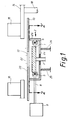
- Figure 1 shows a schematic representation of an arrangement for testing semiconductor wafers, hybrid circuits or the like, with a test table 1, which is used to hold semiconductor wafers and is formed in a known manner on its surface with narrow, preferably circular grooves Serve via a connection system, not shown, to exert a negative pressure in relation to the semiconductor wafer placed thereon and to hold the semiconductor wafer on the test table 1.
- the rehearsal table 1 is also equipped with elements for heating and / or cooling.
- Such a rehearsal table 1 is both in the horizontal plane, i. H. Movable in the X and Y directions, as well as displaceable in a vertical direction.
- an open-topped container 2 is fastened to the bearing 3 of the test table 1, which according to this embodiment can be moved together with the test table 1 and consists of a base 2a and four side walls 2b.
- the side walls 2b have a height such that the test table 1 comes to lie within this container 2 and the surface of the test table 1 comes to lie below the upper edges of the side walls 2b.
- a suitable seal which is not shown in FIG. 1 and which prevents the gas or air in the container 2 from flowing out downward, is arranged between the bearing 3 of the test table 1 and the base 2a.
- outflow elements 5, 6th provided, which are connected to one another via a connecting section 7 (FIG. 2) and are connected to a source 9 via a connection 8.
- the source 9 generates the gas which is led into the interior of the container 2 to produce a laminar flow.
- the connection 8 is carried out through one of the side walls 2b in such a way that the connection 8 is sealed off from the relevant side wall 2b in order to prevent air or gas from escaping.
- the outflow elements 5, 6 can be fixed relative to the bottom 2a or the side walls 2b of the container 2 by holding clips or the like.
- the top of the container 2, which is open at the top, is covered by a plate 10, which contains a central opening 12, which preferably has a circular shape and is aligned centrally with respect to the center of the likewise circular test table 1.
- the plate 10, for example made of sheet metal, is fixed relative to the entire arrangement, so that the test table 1 according to this embodiment can be adjusted together with the container 2 in the horizontal direction relative to the plate 10 and a probe holder 14.
- the probe holder 14 as well as the rehearsal table 1 with its mounting 3 are mounted relative to a frame (not shown), the probe holder 14 being supported relative to the frame 1 by means of a plurality of column guides, optionally adjustable.
- the column guides of the probe holder 14 are designated 18 in FIG.
- Several special holders 15, 16 are mounted on the probe holder 14, which in turn hold the probes to be used and not shown in FIG. 1.
- the opening 12 of the plate 10 is designed in such a way that the probes supported by the probe holders 15, 16 allow a tip contact to the semiconductor wafers to be tested. If necessary, the opening 12 can be closed off by a ring 20, for example made of plexiglass, which also contains a preferably circular opening 22 which is smaller than the opening 12.
- the ring 20 has an outer diameter which is slightly larger than the diameter the opening 12.
- test table 1 is adjusted together with the container 2 in the X and Y directions in order to enable the testing of the individual semiconductor wafers which are arranged on a carrier layer.
- a flow within the container 2 is generated by the outflow elements 5, 6, which flows out evenly from the outflow elements 5, 6 and generates a non-turbulent air flow within the container 2.
- a weak air flow or gas flow is generated in the direction of the opening 12, this air or gas flow emerging evenly from the opening 12. This prevents the entry of ambient air or particles from the environment into the interior of the container 2.
- Cylindrical tubes for example made of ceramic, plastic or synthetic fiber, with a pore density of the order of 1 to 30 ⁇ m are preferably used as outflow elements 5, 6.
- these tubular outflow elements 5, 6 are closed on the side with their free-standing end, whereby the outflow of air or gas is ensured essentially in the radial direction to the outflow elements 5, 6.
- a cooling effect caused by the test table 1 can also be determined, although the temperature is only comparatively lower than that at a surface temperature of the test table 1 of approximately -55 ° C. compared to the dried air supplied by the outflow elements 5, 6 air temperature of, for example, 20 C supplied through the outflow elements 5, 6.
- the cooling effect of the test table 1 is therefore advantageously limited only to the semiconductor wafers to be tested, while other parts within the space of the container 2 are cooled by the test table 1 not be charged.
- the negative pressure generated by the test table 1 for holding the semiconductor wafers is negligible in comparison to the air volume supplied by the outflow elements 5, 6 and does not impair the laminar air flow desired within the container 2.
- the cooling due to the test table 1 in the arrangement described concentrates on the semiconductor wafers placed on it, the rest of the structure largely remains at the temperature that is the temperature of the off flow elements 5, 6 corresponds to air supplied.
- the arrangement according to the invention can also be used to maintain clean room conditions, i. H. for testing semiconductor wafers at temperatures above 0 ° C, e.g. B. at room temperature.
- clean room conditions i. H. for testing semiconductor wafers at temperatures above 0 ° C, e.g. B. at room temperature.
- air with the desired particle purity is introduced into the container 2 and it is prevented that dirt particles enter the container 2 from above via the opening 12.
- the use of clean air is not absolutely necessary, but the supply of filtered air is necessary.
- Another application of the described arrangements is in the testing of semiconductor wafers at higher temperatures. At higher temperatures, needle tip oxidation can occur. Using the arrangement according to the invention, this can be prevented by passing a noble gas (e.g. argon or nitrogen) into the interior of the container 2 through the outflow elements 5, 6 and thereby the test tips of the probes held by the holders 15, 16 are always in a noble gas flow and thus prevent oxidation, which leads to incorrect measurements.
- a noble gas e.g. argon or nitrogen
- the dew point of which is, for example, -60 C
- the ionization of the air has the purpose of avoiding a sparkover within the container 2 when checking the semiconductor wafers.
- the rehearsal table 1 is adjustable relative to the container 2, in particular in the X-Y direction.
- the bottom 2 is provided with a correspondingly large opening, a flexible seal being inserted around the bearing 3 within the opening of the bottom 2a in order to implement the adjustment of the bearing 3 relative to the bottom 2a.
- spring devices 25, 26 are provided in the embodiment shown in FIG. 1, which generate a prestressing force and press the upper edges of the container walls 2b against the lower surface of the plate 10.
- the upward-pointing edges of the side walls 2b are rounded.
- additional sliding elements e.g. the edges of the sliding pins inserted from above are provided.
- the container 2 is preferably made of plexiglass.
- FIG. 2 shows only one possible embodiment of the outflow elements 5, 6, which are arranged essentially parallel to one another and result in an essentially U-shaped or annular structure through a connecting tube 7.
- a corresponding outflow element can be provided, which is connected to the other outflow elements 5, 6.
- the trough-shaped container 2 can be displaced in the horizontal plane to such an extent that it can be accessed by moving it relative to the top plate 10 in the manner of a drawer function in order to to enable replacement of the semiconductor wafers.
- probes in the form of test needles and / or needle edges for contacting the wafers, hybrid circuits or the like can be used.
Abstract
Description
Die Erfindung betrifft eine Anordnung zur Prüfung von Halbleiter-Wafern oder dergleichen gemäß dem Oberbegriff des Patentanspruchs 1.The invention relates to an arrangement for testing semiconductor wafers or the like according to the preamble of patent claim 1.
Die Prüfung von Halbleiter-Wafern wird in Temperaturbereichen von -200 C bis + 400 C durchgeführt. Diese Temperaturwerte werden durch Kühlung und/oder Beheizung eines Probertisches durchgeführt, auf dem die Halbleiter-Wafer zu Prüfzwecken aufgelegt werden. Im Bereich um und unter 0 C werden auf den Wafern sowie auf den Probertischen selbst Eiskristalle erzeugt, die sich infolge der Feuchtigkeit der Umgebungsluft ergeben. Zur Vermeidung derartiger Eiskristalle wird bei manuell bedienbaren Probern ein Stickstoffstrahl auf den Prober gerichtet. Bei dieser Methode wird zwar im Kernbereich des Stickstoffstrahles die Erzeugung von Eiskristallen verhindert, jedoch wird durch das Ansaugen der Umgebungsluft an den Randbereichen des Stickstoffstrahles auf den Halbleiter-Wafern eine Eiskristallbildung nicht verhindert.Semiconductor wafers are tested in temperature ranges from -200 C to + 400 C. These temperature values are carried out by cooling and / or heating a test table on which the semiconductor wafers are placed for testing purposes. In the area around and below 0 C, ice crystals are generated on the wafers and on the test tables themselves, which result from the humidity of the ambient air. To avoid ice crystals of this type, a nitrogen jet is directed onto the prober in manually operated probers. With this method, the generation of ice crystals is prevented in the core area of the nitrogen jet, but ice crystal formation is not prevented by sucking in the ambient air at the edge areas of the nitrogen jet on the semiconductor wafers.
Der Erfindung liegt die Aufgabe zugrunde, eine Anordnung der eingangs genannten Art derart auszubilden, daß im Betrieb bei Temperaturen um und unter 0 C die Erzeugung von Eiskristallen verhindert wird und daß im Betrieb oberhalb von 0°C Beeinträchtigungen durch Staub und/oder Oxidation vermeidbar sind.The invention has for its object to provide an arrangement of the type mentioned in such a way that the production of ice crystals is prevented during operation at temperatures around and below 0 C and that in operation above 0 ° C impairments due to dust and / or oxidation can be avoided .
Diese Aufgabe wird erfindungsgemäß dadurch gelöst, daß der nach oben offene Behälter durch eine Platte abgedeckt ist, die eine Öffnung zur Durchführung von Sonden enthält, und daß innerhalb des Behälters Ausströmelemente vorgesehen sind, die über eine Verbindung an eine Quelle für Luft, Gas oder dergleichen angeschlossen sind.This object is achieved in that the upwardly open container is covered by a plate which contains an opening for the passage of probes, and in that outflow elements are provided within the container which are connected to a source of air, gas or the like are connected.
Die Erfindung schafft eine Anordnung zur Prüfung von Halbleiter-Wafern, mit der bei einer Kühlung durch den Probertisch auf Temperaturen um oder unter 0° C die Erzeugung von Eiskristallen verhindert wird, ferner bei Temperaturen oberhalb von 0° C Reinraumbedingungen einhaltbar sind und bei speziellen Anwendungszwecken Oxidationserscheinungen an den Spitzen der Sonden verhindert werden können.The invention provides an arrangement for testing semiconductor wafers, with which the generation of ice crystals is prevented when the test table is cooled to temperatures around or below 0 ° C., can also be maintained at temperatures above 0 ° C. and for special purposes Oxidation phenomena at the tips of the probes can be prevented.
Bei der erfindungsgemäßen Anordnung ist der Probertisch innerhalb eines nach oben offenen Behälters angeordnet, wobei der Probertisch entweder zusammen mit dem Behälter oder relativ zum Behälter in einer horizontalen Ebene verfahrbar ist. Der nach oben offene Behälter ist durch eine Platte mit einer Öffnung abgeschlossen, wodurch der Probertisch innerhalb eines durch den Behälter und die Platte definierten Raumes angeordnet ist. Durch die Plattenöffnung kontaktieren Sonden die zu prüfenden Halbleiter-Wafer. Zur Vermeidung von Eiskristallbildung und/oder des Eindringens von Staubpartikeln wird über innerhalb des Behälters liegende Ausströmelemente ein Gas bzw. Luft mit der erforderlichen Temperatur und/oder dem gewünschten Taupunkt in den Behälter geleitet. Die Strömungsgeschwindigkeit ist derart gewählt, daß eine laminare Strömung gewährleistet ist und eine vorbestimmte Menge an durch die Plattenöffnung austretender Luft erreicht wird.In the arrangement according to the invention, the rehearsal table is arranged within a container which is open at the top, the rehearsal table being movable in a horizontal plane either together with the container or relative to the container. The container, which is open at the top, is closed by a plate with an opening, as a result of which the test table is arranged within a space defined by the container and the plate. Probes contact the semiconductor wafers to be tested through the plate opening. To avoid ice crystal formation and / or the penetration of dust particles, a gas or air with the required temperature and / or the desired dew point is passed into the container via outflow elements located inside the container. The flow rate is selected in such a way that a laminar flow is ensured and a predetermined amount of air emerging through the plate opening is reached.
Gemäß einer bevorzugten Ausführungsform der erfindungsgemäßen Anordnung bestehen die Ausströmelemente aus porösen Körpern, beispielsweise in Form von zylinderischen Rohren, deren Porösität derart gewählt ist, daß das Gas oder die Luft gleichmäßig über die gesamte Länge der Ausströmelemente in den Innenraum des Behältern austritt und dadurch Turbulenzen innerhalb des Behälters vermieden werden.According to a preferred embodiment of the arrangement according to the invention, the outflow elements consist of porous bodies, for example in the form of cylindrical tubes, the porosity of which is selected in such a way that the gas or air emerges evenly over the entire length of the outflow elements into the interior of the container and thereby turbulence within of the container can be avoided.
Im folgenden wird eine bevorzugte Ausführungsform der erfindungsgemäßen Anordnung anhand der Zeichnung zur Erläuterung weiterer Merkmale beschrieben. Es zeigen:
- Figur 1 eine schematische, teilweise im Schnitt gehaltene Ansicht der Anordnung, und
Figur 2 eine schematische Teilaufsicht auf die Anordnung entlang der Linie 2 - 2'in Figur 1.
- Figure 1 is a schematic, partly in section view of the arrangement, and
- Figure 2 is a schematic partial plan view of the arrangement along the line 2-2 'in Figure 1.
Figur 1 zeigt in schematischer Darstellung eine Anordnung zur Prüfung von Halbleiter-Wafern, Hybridschaltungen oder dergleichen, mit einem Probertisch 1, der zur Aufnahme von Halbleiter-Wafern dient und in bekannter Weise an seiner Oberfläche mit schmalen, vorzugsweise kreisförmigen verlaufenden Nuten ausgebildet ist, die über ein nicht angezeigtes Anschlußsystem dazu dienen, einen Unterdruck gegenüber dem aufgelegten Halbleiter-Wafer auszuüben und den Halbleiter-Wafer auf dem Probertisch 1 zu halten. Der Probertisch 1 ist ferner mit Elementen zur Heizung und/oder Kühlung ausgerüstet. Ein derartiger Probertisch 1 ist sowohl in horizontaler Ebene, d. h. in X- und Y-Richtung verfahrbar, wie auch in einer vertikalen Richtung verlagerbar. Gemäß der dargestellten Ausführungsform der Anordnung ist an der Lagerung 3 des Probertisches 1 eine oben offener Behälter 2 befestigt, der gemäß dieser Ausführungsform zusammen mit dem Probertisch 1 verfahrbar ist und aus einem Boden 2a sowie vier Seitenwänden 2b besteht. Die Seitenwände 2b haben eine Höhe, derart, daß der Probertisch 1 innerhalb dieses Behälters 2 zu liegen kommt und die Oberfläche des Probertisches 1 unterhalb der oberen Kanten der Seitenwände 2b zu liegen kommt. Zwischen der mit 3 bezeichneten Lagerung des Probertisches 1 und dem Boden 2a ist eine geeignete Dichtung angeordnet, die in Figur 1 nicht gezeigt ist und ein Ausströmen des im Behälter 2 befindlichen Gases oder Luft nach unten ausschließt.Figure 1 shows a schematic representation of an arrangement for testing semiconductor wafers, hybrid circuits or the like, with a test table 1, which is used to hold semiconductor wafers and is formed in a known manner on its surface with narrow, preferably circular grooves Serve via a connection system, not shown, to exert a negative pressure in relation to the semiconductor wafer placed thereon and to hold the semiconductor wafer on the test table 1. The rehearsal table 1 is also equipped with elements for heating and / or cooling. Such a rehearsal table 1 is both in the horizontal plane, i. H. Movable in the X and Y directions, as well as displaceable in a vertical direction. According to the illustrated embodiment of the arrangement, an open-
Seitlich des Probertisches 1 sind z. B. in zueinander paralleler Anordnung Ausströmelemente 5, 6 vorgesehen, die über einen Verbindungsabschnitt 7 (Fig. 2) miteinander in Verbindung stehen und über einen Anschluß 8 an eine Quelle 9 angeschlossen sind. Die Quelle 9 erzeugt das Gas, das in das Innere des Behälters 2 geleitet wird, um eine laminare Strömung zu erzeugen. Der Anschluß 8 ist, wie Figur 2 zeigt, durch eine der Seitenwände 2b durchgeführt, derart, daß der Anschluß 8 gegenüber der betreffenden Seitenwand 2b zur Vermeidung eines Austritts von Luft oder Gas abgedichtet ist. Die Ausströmelemente 5, 6 können gegenüber dem Boden 2a oder den Seitenwänden 2b des Behälters 2 durch Halteklammern oder dergleichen fixiert sein.To the side of the rehearsal table 1 are e.g. B. in parallel
Die Oberseite des nach oben offenen Behälters 2 ist durch eine Platte 10 abgedeckt, die eine mittige Öffnung 12 enthält, die vorzugsweise kreisförmige Gestalt hat und mittig gegenüber der Mitte des ebenfalls kreisförmigen Probertisches 1 ausgerichtet ist. Die Platte 10, beispielsweise aus Blech, ist gegenüber der gesamten Anordnung fixiert, so daß der Probertisch 1 gemäß dieser Ausführungsform zusammen mit dem Behälter 2 in horizontaler Richtung gegenüber der Platte 10 und einer Sondenhalterung 14 verstellbar ist.The top of the
Die Sondenhalterung 14 wie auch der Probertisch 1 mit seiner Lagerung 3 sind gegenüber einem nicht gezeigten Rahmen gelagert, wobei die Sondenhalterung 14 durch mehrere Säulenführungen gegenüber dem Rahmen 1, gegebenenfalls verstellbar, gelagert ist. Die Säulenführungen der Sondenhalterung 14 sind in Figur 1 mit 18 bezeichnet. Auf der Sondenhalterung 14 sind mehrere Sonderhalter 15, 16 montiert, die ihrerseits die zu benutzenden und in Figur 1 nicht gezeigten Sonden aufnehmen.The
Die Öffnung 12 der Platte 10 ist derart konzipiert, daß die von den Sondenhaltern 15, 16 gelagerten Sonden einen Spitzenkontakt zu den zu prüfenden Halbleiter-Wafern ermöglichen. Im Bedarfsfall kann die Öffnung 12 durch einen Ring 20, beispielsweise aus Plexiglas, abgeschlossen werden, der eine ebenfalls vorzugsweise kreisförmige Öffnung 22 enthält, welche kleiner ist als die Öffnung 12. Der Ring 20 hat dabei einen Außendurchmesser, der geringfügig größer ist als der Durchmesser der Öffnung 12.The
Mittels des Ringes 20, der entweder auf der Platte 10 aufliegt oder in eine ringförmige Nut der Platte 10 im Bereich deren Öffnung 12 eingesetzt wird, die seitlich der Öffnung 12 ausgebildet ist, wird eine Verringerung des Querschnittes der Öffnung 12 im Bedarfsfalle erreicht.By means of the
Bei der in Figur 1 und 2 gezeigten Ausführungsform ist eine Verstellung des Probertisches 1 gegenüber der Sondenhalterung 14 und den in den Sondenhaltern 15, 16 eingespannten Sonden möglich, um ein schrittweises Abtasten der auf dem Probertisch 1 aufliegenden Halbleiter-Wafern zu realisieren. Gemäß der dargestellten Ausführungsform wird der Probertisch 1 zusammen mit dem Behälter 2 in X- und Y-Richtung verstellt, um die Prüfung der einzelnen Halbleiter-Wafer zu ermöglichen, die auf einer Trägerschicht angeordnet sind.In the embodiment shown in FIGS. 1 and 2, an adjustment of the test table 1 with respect to the
Durch die Ausströmelemente 5, 6 wird eine Strömung innerhalb des Behälters 2 erzeugt, die gleichmäßig aus den Ausströmelementen 5, 6 austritt und eine nicht turbulente Luftströmung innerhalb des Behälters 2 erzeugt. Hierdurch wird ein schwacher Luftstrom oder Gasstrom in Richtung der Öffnung 12 erzeugt, wobei diese Luft- oder Gasströmung gleichmäßig aus der Öffnung 12 austritt. Dadurch wird der Eintritt von Umgebungsluft oder von Partikeln aus der Umgebung in das Innere des Behälters 2 verindert.A flow within the
Als Ausströmelemente 5, 6 dienen vorzugsweise zylinderische Rohre, beispielsweise aus Keramik, Kunststoff oder Kunstfaser, mit einer Porendichte in Größenordnung von 1 bis 30 um. Diese rohrförmigen Ausströmelemente 5, 6 sind gemäß Figur 2 an der Seite mit ihrem freistehenden Ende abgeschlossen, wodurch das Ausströmen von Luft oder Gas im wesentlichen in Radialrichtung zu den Ausströmelementen 5, 6 gewährleistet ist. Untersuchungen haben gezeigt, daß bei einer Anordnung mit dem vorstehend beschriebenen Aufbau stets eine konstante Luftvolumenemission aus der Öffnung 12 gegeben ist, wobei die Luft nur geringfügig abgekühlt wird, nachdem sie an der Oberfläche der zu prüfenden Halbleiter-Wafer passiert ist. Unterhalb des Probertisches 1 ist ebenfalls ein durch den Probertisch 1 hervorgerufener Kühleffekt festzustellen, wobei die Temperatur allerdings im Vergleich zu der durch die Ausströmelemente 5, 6 zugeführten, getrockneten Luft bei einer Oberflächentemperatur des Probertisches 1 von etwa - 55 C nur verhältnismäßig niedriger ist als die durch die Ausströmelemente 5, 6 zugeführte Lufttemperatur von beispielsweise 20 C. Damit beschränkt sich bei der beschriebenen Anordnung der Kühleffekt des Probertisches 1 vorteilhafterweise nur auf die zu prüfenden Halbleiter-Wafer, während andere Teile innerhalb des Raumes des Behälters 2 durch die Kühlung des Probertischs 1 nicht beaufschlagt werden.Cylindrical tubes, for example made of ceramic, plastic or synthetic fiber, with a pore density of the order of 1 to 30 μm are preferably used as
Der vom Probertisch 1 erzeugte Unterdruck zur Halterung der Halbleiter-Wafer ist im Vergleich zu dem von den Ausströmelementen 5, 6 zugeführten Luftvolumen vernachlässigbar und beeinträchtigt nicht die innerhalb des Behälters 2 gewünschte laminare Luftströmung.The negative pressure generated by the test table 1 for holding the semiconductor wafers is negligible in comparison to the air volume supplied by the
Somit konzentriert sich die Kühlung aufgrund des Probertisches 1 bei der beschriebenen Anordnung auf die aufgelegten Halbleiter-Wafer, der übrige Aufbau verbleibt weitgehend auf derjenigen Temperatur, die der Temperatur der durch die Ausströmelemente 5, 6 zugeführten Luft entspricht.Thus, the cooling due to the test table 1 in the arrangement described concentrates on the semiconductor wafers placed on it, the rest of the structure largely remains at the temperature that is the temperature of the
Die erfindungsgemäße Anordnung läßt sich auch zur Einhaltung von Reinraumbedingungen einsetzen, d. h. für die Prüfung von Halbleiter-Wafern bei Temperaturen oberhalb von 0 ° C, z. B. bei Raumtemperatur. Bei dieser Anwendungsart wird Luft mit der jeweils gewünschten Partikelreinheit in den Behälter 2 eingeführt und es wird verhindert, daß von oben über die Öffnung 12 Schmutzpartikel in den Behälter 2 eintreten. Bei Anwendung der beschriebenen Anordnung unter Reinraumbedingungen bedarf es nicht unbedingt des Einsatzes reiner Luft, jedoch der Zuführung von gefilterter Luft.The arrangement according to the invention can also be used to maintain clean room conditions, i. H. for testing semiconductor wafers at temperatures above 0 ° C, e.g. B. at room temperature. In this type of application, air with the desired particle purity is introduced into the
Eine weitere Anwendung der beschriebenen Anordnungen liegt in der Überprüfung von Halbleiter-Wafern bei höheren Temperaturen. Bei höheren Temperaturen können an den Nadelspitzen Oxidationen auftreten. Unter Einsatz der erfindungsgemäßen Anordnung läßt sich dies dadurch verhindern, daß durch die Ausströmelemente 5, 6 ein Edelgas (z. B. Argon oder Stickstoff) in den Innenraum des Behälters 2 geleitet wird und dadurch die Prüfspitzen der von den Haltern 15, 16 gehalterten Sonden sich stets in einem Edelgasstrom befinden und dadurch Oxidationen, die zu Fehlmessungen führen, verhindert werden.Another application of the described arrangements is in the testing of semiconductor wafers at higher temperatures. At higher temperatures, needle tip oxidation can occur. Using the arrangement according to the invention, this can be prevented by passing a noble gas (e.g. argon or nitrogen) into the interior of the
Wird die erfindungsgemäße Anordnung in Verbindung mit getrockneter Luft verwendet, deren Taupunkt beispielsweise bei -60 C liegt, kann es erforderlich sein, in dem Behälter 2 eine lonisationseinrichtung vorzusehen, um die zu den Ausströmelementen 5, 6 geführte Luft vor deren Eintriff in den Behälter 2 zu ionisieren. Die lonisierung der Luft hat den Zweck, einen Funkenüberschlag innerhalb des Behälters 2 bei der Überprüfung der Halbleiter-Wafer zu vermeiden.If the arrangement according to the invention is used in connection with dried air, the dew point of which is, for example, -60 C, it may be necessary to provide an ionization device in the
Gemäß einer weiteren, in den Zeichnungen nicht dargestellten Ausführungsform der erfindungsgemäßen Anordnung ist vorgesehen, daß der Probertisch 1 relativ zum Behälter 2 verstellbar, insbesondere in X-Y-Richtung verstellbar ist. Um dies zu erreichen, ist der Boden 2 mit einer entsprechend großen Öffnung versehen, wobei innerhalb der Öffnung des Bodens 2a um die Lagerung 3 eine flexible Dichtung eingesetzt ist, um die Verstellung der Lagerung 3 relativ zum Boden 2a zu realisieren.According to a further embodiment of the arrangement according to the invention, not shown in the drawings, it is provided that the rehearsal table 1 is adjustable relative to the
Um den Behälter 2 gegen die Unterfläche der Platte 10 zu halten, sind bei der in Figur 1 gezeigten Ausführungsform Federeinrichtungen 25, 26 vorgesehen, die eine Vorspannungskraft erzeugen und die oberen Kanten der Behälterwände 2b gegen die untere Fläche der Platte 10 drücken.In order to hold the
Um eine ruckfreie Verschiebung des Behälters 2 gegenüber der Platte 10 zu vermeiden, d. h. um den Reibungswiderstand zwischen den oberen Kanten der Seitenwände 2b und der Platte 10 weitgehend zu reduzieren, sind bei einer bevorzugten Ausführungsform die nach oben weisenden Kanten der Seitenwände 2b abgerundet. Anstelle der Abrundungen der Kanten der Seitenwände 2b können zusätzliche Gleitelemente, z.B. die Kanten von oben eingesetzten Gleitstiften, vorgesehen werden.In order to avoid a smooth displacement of the
Zur besseren Einsicht in den Behälter 2 besteht dieser vorzugsweise aus Plexiglas.For better insight into the
Figur 2 zeigt nur eine mögliche Ausführungsform der Ausströmelemente 5, 6, die im wesentlichen parallel zueinander liegend angeordnet sind und durch ein Verbindungsrohr 7 eine im wesentliche U-förmige oder ringförmige Struktur ergeben. Anstelle des Verbindungsrohres 7 kann ein entsprechendes Ausströmelement vorgesehen sein, das mit den anderen Ausströmelementen 5, 6 verbunden ist.FIG. 2 shows only one possible embodiment of the
Die erfindungsgemäße Anordnung läßt sich in der nachstehenden Weise verwenden:
- Bei Prüfvorgängen in Temperaturbereichen von - 200° C bis + 400 C, die vom Probertisch 1 an seiner Oberfläche gegenüber den aufliegenden Halbleiter-Wafern erzeugt werden, wird zur Vermeidung von Eiskristallbildung von der
Quelle 9 eine Luftströmung erzeugt, die beispielsweise eine Temperatur von 20 C hat und einen Taupunkt bei ungefähr -60 C besitzt.
- In test processes in temperature ranges from - 200 ° C to + 400 C, which are generated by the test table 1 on its surface opposite the semiconductor wafers lying on it, an air flow is generated from the
source 9 to prevent ice crystal formation, for example, a temperature of 20 C and has a dew point at around -60 C.
Bei der erfindungsgemäßen Anordnung, die sich insbesondere für manuell bedienbare Prober eignet, läßt sich der wannenförmige Behälter 2 soweit in der horizontalen Ebene verschieben, daß er durch Verlagerung gegenüber der oben liegenden Platte 10 nach Art einer Schubladenfunktion den Zugang auf den Probertisch 1 ermöglicht, um ein Auswechseln der Halbleiter-Wafer zu ermöglichen.In the arrangement according to the invention, which is particularly suitable for manually operated probers, the trough-shaped
Bei der Überprüfung von Wafern können Sonden in Form von Prüfnadeln und/oder Nadelkanten zum Kontaktieren der Wafer, Hybridschaltungen oder dergleichen eingesetzt werden.When checking wafers, probes in the form of test needles and / or needle edges for contacting the wafers, hybrid circuits or the like can be used.
Claims (8)
Applications Claiming Priority (2)
| Application Number | Priority Date | Filing Date | Title |
|---|---|---|---|
| DE4109908A DE4109908C2 (en) | 1991-03-26 | 1991-03-26 | Arrangement for testing semiconductor wafers |
| DE4109908 | 1991-03-26 |
Publications (3)
| Publication Number | Publication Date |
|---|---|
| EP0505981A2 true EP0505981A2 (en) | 1992-09-30 |
| EP0505981A3 EP0505981A3 (en) | 1994-04-06 |
| EP0505981B1 EP0505981B1 (en) | 1998-06-10 |
Family
ID=6428242
Family Applications (1)
| Application Number | Title | Priority Date | Filing Date |
|---|---|---|---|
| EP92105051A Expired - Lifetime EP0505981B1 (en) | 1991-03-26 | 1992-03-24 | Semiconductor wafer testing device |
Country Status (6)
| Country | Link |
|---|---|
| US (1) | US5220277A (en) |
| EP (1) | EP0505981B1 (en) |
| JP (1) | JP2719068B2 (en) |
| AT (1) | ATE167304T1 (en) |
| DE (2) | DE4109908C2 (en) |
| ES (1) | ES2117017T3 (en) |
Cited By (3)
| Publication number | Priority date | Publication date | Assignee | Title |
|---|---|---|---|---|
| US6745575B2 (en) | 2002-07-11 | 2004-06-08 | Temptronic Corporation | Workpiece chuck with temperature control assembly having spacers between layers providing clearance for thermoelectric modules |
| US6886347B2 (en) | 2002-07-11 | 2005-05-03 | Temptronic Corporation | Workpiece chuck with temperature control assembly having spacers between layers providing clearance for thermoelectric modules |
| WO2010028914A1 (en) * | 2008-09-15 | 2010-03-18 | Suss Microtec Test Systems Gmbh | Method for verifying a test substrate in a prober under defined thermal conditions |
Families Citing this family (44)
| Publication number | Priority date | Publication date | Assignee | Title |
|---|---|---|---|---|
| US5829128A (en) | 1993-11-16 | 1998-11-03 | Formfactor, Inc. | Method of mounting resilient contact structures to semiconductor devices |
| US5476211A (en) | 1993-11-16 | 1995-12-19 | Form Factor, Inc. | Method of manufacturing electrical contacts, using a sacrificial member |
| US6313649B2 (en) | 1992-06-11 | 2001-11-06 | Cascade Microtech, Inc. | Wafer probe station having environment control enclosure |
| US6380751B2 (en) | 1992-06-11 | 2002-04-30 | Cascade Microtech, Inc. | Wafer probe station having environment control enclosure |
| US5345170A (en) * | 1992-06-11 | 1994-09-06 | Cascade Microtech, Inc. | Wafer probe station having integrated guarding, Kelvin connection and shielding systems |
| US20020053734A1 (en) | 1993-11-16 | 2002-05-09 | Formfactor, Inc. | Probe card assembly and kit, and methods of making same |
| US5610529A (en) * | 1995-04-28 | 1997-03-11 | Cascade Microtech, Inc. | Probe station having conductive coating added to thermal chuck insulator |
| DE19540103B4 (en) * | 1995-10-27 | 2008-04-17 | Erich Reitinger | Test device for semiconductor wafers to be tested by means of test tools |
| DE19615674A1 (en) * | 1996-04-19 | 1997-10-23 | Mci Computer Gmbh | Measuring device for integrated circuits |
| US5963027A (en) * | 1997-06-06 | 1999-10-05 | Cascade Microtech, Inc. | Probe station having environment control chambers with orthogonally flexible lateral wall assembly |
| US6002263A (en) | 1997-06-06 | 1999-12-14 | Cascade Microtech, Inc. | Probe station having inner and outer shielding |
| US6034533A (en) * | 1997-06-10 | 2000-03-07 | Tervo; Paul A. | Low-current pogo probe card |
| US6445202B1 (en) | 1999-06-30 | 2002-09-03 | Cascade Microtech, Inc. | Probe station thermal chuck with shielding for capacitive current |
| AU2117101A (en) * | 1999-10-19 | 2001-04-30 | Solid State Measurements, Inc. | Non-invasive electrical measurement of semiconductor wafers |
| US6838890B2 (en) * | 2000-02-25 | 2005-01-04 | Cascade Microtech, Inc. | Membrane probing system |
| US6700397B2 (en) | 2000-07-13 | 2004-03-02 | The Micromanipulator Company, Inc. | Triaxial probe assembly |
| US6424141B1 (en) * | 2000-07-13 | 2002-07-23 | The Micromanipulator Company, Inc. | Wafer probe station |
| US6965226B2 (en) | 2000-09-05 | 2005-11-15 | Cascade Microtech, Inc. | Chuck for holding a device under test |
| US6914423B2 (en) | 2000-09-05 | 2005-07-05 | Cascade Microtech, Inc. | Probe station |
| US6628131B1 (en) * | 2000-11-06 | 2003-09-30 | Intel Corporation | Test unit and enclosure for testing integrated circuits |
| US6951846B2 (en) * | 2002-03-07 | 2005-10-04 | The United States Of America As Represented By The Secretary Of The Army | Artemisinins with improved stability and bioavailability for therapeutic drug development and application |
| US7750654B2 (en) | 2002-09-02 | 2010-07-06 | Octec Inc. | Probe method, prober, and electrode reducing/plasma-etching processing mechanism |
| DE10246282B4 (en) * | 2002-10-02 | 2005-12-29 | Suss Microtec Test Systems Gmbh | Prober for testing substrates at low temperatures |
| US7248062B1 (en) | 2002-11-04 | 2007-07-24 | Kla-Tencor Technologies Corp. | Contactless charge measurement of product wafers and control of corona generation and deposition |
| US6847219B1 (en) | 2002-11-08 | 2005-01-25 | Cascade Microtech, Inc. | Probe station with low noise characteristics |
| US6861856B2 (en) * | 2002-12-13 | 2005-03-01 | Cascade Microtech, Inc. | Guarded tub enclosure |
| US7492172B2 (en) | 2003-05-23 | 2009-02-17 | Cascade Microtech, Inc. | Chuck for holding a device under test |
| US7250626B2 (en) | 2003-10-22 | 2007-07-31 | Cascade Microtech, Inc. | Probe testing structure |
| US7187188B2 (en) | 2003-12-24 | 2007-03-06 | Cascade Microtech, Inc. | Chuck with integrated wafer support |
| DE102004062592B3 (en) * | 2004-12-24 | 2006-06-08 | Leica Microsystems Jena Gmbh | Disk-shaped substrate testing system, has suction unit arranged at side of housing and spaced from mounting plate, and opening provided in suction unit, where opening has width that corresponds to distance of plate to wall of housing |
| US7535247B2 (en) | 2005-01-31 | 2009-05-19 | Cascade Microtech, Inc. | Interface for testing semiconductors |
| US7656172B2 (en) | 2005-01-31 | 2010-02-02 | Cascade Microtech, Inc. | System for testing semiconductors |
| US20060177160A1 (en) * | 2005-02-07 | 2006-08-10 | Wagner James C | Disposable bag for particularized waste |
| US20070294047A1 (en) * | 2005-06-11 | 2007-12-20 | Leonard Hayden | Calibration system |
| WO2007022538A2 (en) | 2005-08-19 | 2007-02-22 | Kla-Tencor Technologies Corporation | Test pads for measuring properties of a wafer |
| JP4605387B2 (en) * | 2005-12-12 | 2011-01-05 | 住友電気工業株式会社 | Temperature characteristic inspection device |
| US7562617B2 (en) * | 2006-05-15 | 2009-07-21 | Centipede Systems, Inc. | Mounting apparatus |
| US7764076B2 (en) * | 2007-02-20 | 2010-07-27 | Centipede Systems, Inc. | Method and apparatus for aligning and/or leveling a test head |
| KR101492408B1 (en) * | 2007-10-10 | 2015-02-12 | 캐스캐이드 마이크로텍 드레스덴 게엠베하 | Method for testing a test substrate under defined thermal conditions and thermally conditionable prober |
| WO2009064285A1 (en) * | 2007-11-13 | 2009-05-22 | Testmetrix, Inc. | Apparatus and method for testing semiconductor devices |
| US8319503B2 (en) | 2008-11-24 | 2012-11-27 | Cascade Microtech, Inc. | Test apparatus for measuring a characteristic of a device under test |
| IT201800007609A1 (en) * | 2018-07-30 | 2020-01-30 | Microtest Srl | An integrated machine for conducting temperature tests on electronic components such as chips |
| DE102021211263A1 (en) | 2021-10-06 | 2023-04-06 | Ers Electronic Gmbh | Shielding device for a chuck, corresponding chuck and corresponding wafer prober arrangement |
| CN116148578B (en) * | 2023-02-28 | 2023-07-21 | 浙江科瑞信电子科技有限公司 | Probe contact device with carrier plate buffer |
Citations (7)
| Publication number | Priority date | Publication date | Assignee | Title |
|---|---|---|---|---|
| US3710251A (en) * | 1971-04-07 | 1973-01-09 | Collins Radio Co | Microelectric heat exchanger pedestal |
| US4607220A (en) * | 1984-05-07 | 1986-08-19 | The Micromanipulator Co., Inc. | Method and apparatus for low temperature testing of electronic components |
| US4845426A (en) * | 1987-05-20 | 1989-07-04 | Signatone Corporation | Temperature conditioner for tests of unpackaged semiconductors |
| EP0341156A1 (en) * | 1988-05-06 | 1989-11-08 | Carrier S.A. | Device for supporting and thermally regulating a piece and semi-conductor circuit plates testing apparatus comprising such a device |
| DE3914699A1 (en) * | 1988-05-05 | 1989-11-16 | Gourdon S A Ets | TEMPERATURE-CONDUCTING CARRIER FOR SMALL OBJECTS, SEMICONDUCTOR COMPONENTS, AND METHOD FOR THERMAL CONTROL WITH USE OF THIS CARRIER |
| FR2645679A1 (en) * | 1989-04-07 | 1990-10-12 | Onera (Off Nat Aerospatiale) | Test installation, in particular for semiconductor wafers |
| US5084671A (en) * | 1987-09-02 | 1992-01-28 | Tokyo Electron Limited | Electric probing-test machine having a cooling system |
Family Cites Families (14)
| Publication number | Priority date | Publication date | Assignee | Title |
|---|---|---|---|---|
| DE255410C (en) * | 1911-05-16 | 1913-01-08 | ||
| DE2753684C2 (en) * | 1977-12-02 | 1982-09-30 | Erich 8000 München Reitinger | Rotatable support table for automatic probers for holding wafers |
| JPS61131834U (en) * | 1985-02-06 | 1986-08-18 | ||
| US4665360A (en) * | 1985-03-11 | 1987-05-12 | Eaton Corporation | Docking apparatus |
| JPS6211243A (en) * | 1985-07-04 | 1987-01-20 | Hitachi Electronics Eng Co Ltd | Prober device having temperature control means |
| US4757255A (en) * | 1986-03-03 | 1988-07-12 | National Semiconductor Corporation | Environmental box for automated wafer probing |
| JPS6367980U (en) * | 1986-10-22 | 1988-05-07 | ||
| DD255410A1 (en) * | 1986-12-23 | 1988-03-30 | Tech Mikroelektronik Forsch | HEATABLE DISK PLATE FOR AUTOMATIC WAF PROP |
| JPH07111455B2 (en) * | 1987-12-15 | 1995-11-29 | 東京エレクトロン株式会社 | Probe device |
| JPH07111995B2 (en) * | 1987-09-02 | 1995-11-29 | 東京エレクトロン株式会社 | Probe device |
| JP2653075B2 (en) * | 1987-12-25 | 1997-09-10 | 株式会社デンソー | Multiprocessor control unit |
| JPH022144A (en) * | 1988-06-13 | 1990-01-08 | Tokyo Electron Ltd | Method of probing semiconductor wafer |
| US4968931A (en) * | 1989-11-03 | 1990-11-06 | Motorola, Inc. | Apparatus and method for burning in integrated circuit wafers |
| JPH03184355A (en) * | 1989-12-13 | 1991-08-12 | Mitsubishi Electric Corp | Wafer prober |
-
1991
- 1991-03-26 DE DE4109908A patent/DE4109908C2/en not_active Expired - Lifetime
-
1992
- 1992-03-24 ES ES92105051T patent/ES2117017T3/en not_active Expired - Lifetime
- 1992-03-24 AT AT92105051T patent/ATE167304T1/en active
- 1992-03-24 DE DE59209366T patent/DE59209366D1/en not_active Expired - Lifetime
- 1992-03-24 EP EP92105051A patent/EP0505981B1/en not_active Expired - Lifetime
- 1992-03-24 JP JP4065687A patent/JP2719068B2/en not_active Expired - Fee Related
- 1992-03-25 US US07/856,256 patent/US5220277A/en not_active Expired - Lifetime
Patent Citations (7)
| Publication number | Priority date | Publication date | Assignee | Title |
|---|---|---|---|---|
| US3710251A (en) * | 1971-04-07 | 1973-01-09 | Collins Radio Co | Microelectric heat exchanger pedestal |
| US4607220A (en) * | 1984-05-07 | 1986-08-19 | The Micromanipulator Co., Inc. | Method and apparatus for low temperature testing of electronic components |
| US4845426A (en) * | 1987-05-20 | 1989-07-04 | Signatone Corporation | Temperature conditioner for tests of unpackaged semiconductors |
| US5084671A (en) * | 1987-09-02 | 1992-01-28 | Tokyo Electron Limited | Electric probing-test machine having a cooling system |
| DE3914699A1 (en) * | 1988-05-05 | 1989-11-16 | Gourdon S A Ets | TEMPERATURE-CONDUCTING CARRIER FOR SMALL OBJECTS, SEMICONDUCTOR COMPONENTS, AND METHOD FOR THERMAL CONTROL WITH USE OF THIS CARRIER |
| EP0341156A1 (en) * | 1988-05-06 | 1989-11-08 | Carrier S.A. | Device for supporting and thermally regulating a piece and semi-conductor circuit plates testing apparatus comprising such a device |
| FR2645679A1 (en) * | 1989-04-07 | 1990-10-12 | Onera (Off Nat Aerospatiale) | Test installation, in particular for semiconductor wafers |
Cited By (3)
| Publication number | Priority date | Publication date | Assignee | Title |
|---|---|---|---|---|
| US6745575B2 (en) | 2002-07-11 | 2004-06-08 | Temptronic Corporation | Workpiece chuck with temperature control assembly having spacers between layers providing clearance for thermoelectric modules |
| US6886347B2 (en) | 2002-07-11 | 2005-05-03 | Temptronic Corporation | Workpiece chuck with temperature control assembly having spacers between layers providing clearance for thermoelectric modules |
| WO2010028914A1 (en) * | 2008-09-15 | 2010-03-18 | Suss Microtec Test Systems Gmbh | Method for verifying a test substrate in a prober under defined thermal conditions |
Also Published As
| Publication number | Publication date |
|---|---|
| ES2117017T3 (en) | 1998-08-01 |
| EP0505981A3 (en) | 1994-04-06 |
| US5220277A (en) | 1993-06-15 |
| EP0505981B1 (en) | 1998-06-10 |
| DE4109908C2 (en) | 1994-05-05 |
| ATE167304T1 (en) | 1998-06-15 |
| JPH06104321A (en) | 1994-04-15 |
| JP2719068B2 (en) | 1998-02-25 |
| DE4109908A1 (en) | 1992-10-01 |
| DE59209366D1 (en) | 1998-07-16 |
Similar Documents
| Publication | Publication Date | Title |
|---|---|---|
| EP0505981B1 (en) | Semiconductor wafer testing device | |
| DE3511165C2 (en) | ||
| DE2807262C2 (en) | Container arrangement with a completely emptying sample vessel | |
| DE3028154C2 (en) | Specimen holder for inverted microscopes | |
| DE3738840C2 (en) | ||
| DE4012600C2 (en) | Microtome | |
| DE112008002615B4 (en) | Method for testing a test substrate under defined thermal conditions and thermally conditionable prober | |
| DE102006018474A1 (en) | Test device for semiconductor elements on a semiconductor wafer and a test method using the test device | |
| DE102008047337A1 (en) | Method for testing a test substrate in a prober under defined thermal conditions | |
| DE60020329T2 (en) | Arrangement and method for collecting and detecting hydrogen | |
| DE10246282B4 (en) | Prober for testing substrates at low temperatures | |
| DE4343810C1 (en) | Photoelectric measuring head | |
| DE19801117C1 (en) | Quality testing of a flat element at limited test area | |
| WO2015078445A1 (en) | Needle guide for biopsy | |
| DE102008053942A1 (en) | Incubator device and method | |
| DE102004030881A1 (en) | Contact area contacting method for prober, involves observing vertical movement of semiconductor wafer along observation axis which runs in plane that is slight distance away from free wafer surface in its expected end position | |
| DE3016483A1 (en) | Electronic PCB test device - has contact pins with pneumatically applied test heads and arranged on carrier plate | |
| DE2143085A1 (en) | Method and device for drilling a side channel branching off from a channel | |
| DE2646888A1 (en) | DEVICE FOR THERMAL TENSIONING OF GLASS PANELS WITH AIR | |
| DE3220619C2 (en) | Device for handling thin sections, in particular cryosections, and method for freeze-drying such thin sections | |
| DE2937652C2 (en) | Nozzle for supplying gases | |
| DE4315441A1 (en) | Clamping (mounting, chucking) and locating unit for a set of components for measurement purposes | |
| WO2023057143A1 (en) | Shielding device for a chuck, corresponding chuck, and corresponding wafer prober assembly | |
| DE3026148C2 (en) | Device for checking the passage of a vessel | |
| DE604919C (en) | Device for distributing air or gases in liquids |
Legal Events
| Date | Code | Title | Description |
|---|---|---|---|
| PUAI | Public reference made under article 153(3) epc to a published international application that has entered the european phase |
Free format text: ORIGINAL CODE: 0009012 |
|
| AK | Designated contracting states |
Kind code of ref document: A2 Designated state(s): AT BE CH DE DK ES FR GB GR IT LI LU NL SE |
|
| PUAL | Search report despatched |
Free format text: ORIGINAL CODE: 0009013 |
|
| AK | Designated contracting states |
Kind code of ref document: A3 Designated state(s): AT BE CH DE DK ES FR GB GR IT LI LU NL SE |
|
| 17P | Request for examination filed |
Effective date: 19940510 |
|
| 17Q | First examination report despatched |
Effective date: 19961007 |
|
| GRAG | Despatch of communication of intention to grant |
Free format text: ORIGINAL CODE: EPIDOS AGRA |
|
| GRAG | Despatch of communication of intention to grant |
Free format text: ORIGINAL CODE: EPIDOS AGRA |
|
| GRAH | Despatch of communication of intention to grant a patent |
Free format text: ORIGINAL CODE: EPIDOS IGRA |
|
| GRAH | Despatch of communication of intention to grant a patent |
Free format text: ORIGINAL CODE: EPIDOS IGRA |
|
| GRAA | (expected) grant |
Free format text: ORIGINAL CODE: 0009210 |
|
| AK | Designated contracting states |
Kind code of ref document: B1 Designated state(s): AT BE CH DE DK ES FR GB GR IT LI LU NL SE |
|
| PG25 | Lapsed in a contracting state [announced via postgrant information from national office to epo] |
Ref country code: GR Free format text: LAPSE BECAUSE OF NON-PAYMENT OF DUE FEES Effective date: 19980610 |
|
| REF | Corresponds to: |
Ref document number: 167304 Country of ref document: AT Date of ref document: 19980615 Kind code of ref document: T |
|
| REG | Reference to a national code |
Ref country code: CH Ref legal event code: NV Representative=s name: HEPP, WENGER & RYFFEL AG Ref country code: CH Ref legal event code: EP |
|
| GBT | Gb: translation of ep patent filed (gb section 77(6)(a)/1977) |
Effective date: 19980611 |
|
| REF | Corresponds to: |
Ref document number: 59209366 Country of ref document: DE Date of ref document: 19980716 |
|
| REG | Reference to a national code |
Ref country code: ES Ref legal event code: FG2A Ref document number: 2117017 Country of ref document: ES Kind code of ref document: T3 |
|
| ET | Fr: translation filed | ||
| ITF | It: translation for a ep patent filed |
Owner name: STUDIO TORTA S.R.L. |
|
| PG25 | Lapsed in a contracting state [announced via postgrant information from national office to epo] |
Ref country code: DK Free format text: LAPSE BECAUSE OF FAILURE TO SUBMIT A TRANSLATION OF THE DESCRIPTION OR TO PAY THE FEE WITHIN THE PRESCRIBED TIME-LIMIT Effective date: 19980910 |
|
| PG25 | Lapsed in a contracting state [announced via postgrant information from national office to epo] |
Ref country code: LU Free format text: LAPSE BECAUSE OF NON-PAYMENT OF DUE FEES Effective date: 19990324 |
|
| PG25 | Lapsed in a contracting state [announced via postgrant information from national office to epo] |
Ref country code: BE Free format text: LAPSE BECAUSE OF NON-PAYMENT OF DUE FEES Effective date: 19990331 |
|
| PLBE | No opposition filed within time limit |
Free format text: ORIGINAL CODE: 0009261 |
|
| STAA | Information on the status of an ep patent application or granted ep patent |
Free format text: STATUS: NO OPPOSITION FILED WITHIN TIME LIMIT |
|
| 26N | No opposition filed | ||
| BERE | Be: lapsed |
Owner name: REITINGER ERICH Effective date: 19990331 |
|
| REG | Reference to a national code |
Ref country code: GB Ref legal event code: IF02 |
|
| PGFP | Annual fee paid to national office [announced via postgrant information from national office to epo] |
Ref country code: NL Payment date: 20100304 Year of fee payment: 19 |
|
| PGFP | Annual fee paid to national office [announced via postgrant information from national office to epo] |
Ref country code: SE Payment date: 20100310 Year of fee payment: 19 |
|
| PGFP | Annual fee paid to national office [announced via postgrant information from national office to epo] |
Ref country code: GB Payment date: 20110330 Year of fee payment: 20 Ref country code: DE Payment date: 20110331 Year of fee payment: 20 Ref country code: FR Payment date: 20110421 Year of fee payment: 20 |
|
| PGFP | Annual fee paid to national office [announced via postgrant information from national office to epo] |
Ref country code: IT Payment date: 20110331 Year of fee payment: 20 |
|
| REG | Reference to a national code |
Ref country code: NL Ref legal event code: V1 Effective date: 20111001 |
|
| PGFP | Annual fee paid to national office [announced via postgrant information from national office to epo] |
Ref country code: CH Payment date: 20110830 Year of fee payment: 20 |
|
| REG | Reference to a national code |
Ref country code: SE Ref legal event code: EUG |
|
| PGFP | Annual fee paid to national office [announced via postgrant information from national office to epo] |
Ref country code: ES Payment date: 20110926 Year of fee payment: 20 Ref country code: AT Payment date: 20110922 Year of fee payment: 20 |
|
| PG25 | Lapsed in a contracting state [announced via postgrant information from national office to epo] |
Ref country code: NL Free format text: LAPSE BECAUSE OF NON-PAYMENT OF DUE FEES Effective date: 20111001 |
|
| REG | Reference to a national code |
Ref country code: DE Ref legal event code: R071 Ref document number: 59209366 Country of ref document: DE |
|
| REG | Reference to a national code |
Ref country code: DE Ref legal event code: R071 Ref document number: 59209366 Country of ref document: DE |
|
| REG | Reference to a national code |
Ref country code: CH Ref legal event code: PL |
|
| REG | Reference to a national code |
Ref country code: GB Ref legal event code: PE20 Expiry date: 20120323 |
|
| PG25 | Lapsed in a contracting state [announced via postgrant information from national office to epo] |
Ref country code: DE Free format text: LAPSE BECAUSE OF EXPIRATION OF PROTECTION Effective date: 20120326 |
|
| PG25 | Lapsed in a contracting state [announced via postgrant information from national office to epo] |
Ref country code: GB Free format text: LAPSE BECAUSE OF EXPIRATION OF PROTECTION Effective date: 20120323 |
|
| REG | Reference to a national code |
Ref country code: AT Ref legal event code: MK07 Ref document number: 167304 Country of ref document: AT Kind code of ref document: T Effective date: 20120324 |
|
| PG25 | Lapsed in a contracting state [announced via postgrant information from national office to epo] |
Ref country code: SE Free format text: LAPSE BECAUSE OF NON-PAYMENT OF DUE FEES Effective date: 20110325 |
|
| REG | Reference to a national code |
Ref country code: ES Ref legal event code: FD2A Effective date: 20130718 |
|
| PG25 | Lapsed in a contracting state [announced via postgrant information from national office to epo] |
Ref country code: ES Free format text: LAPSE BECAUSE OF EXPIRATION OF PROTECTION Effective date: 20120325 |