EP0465693A1 - Electrical insulating printed circuit board with integrated cooling means - Google Patents
Electrical insulating printed circuit board with integrated cooling means Download PDFInfo
- Publication number
- EP0465693A1 EP0465693A1 EP90113092A EP90113092A EP0465693A1 EP 0465693 A1 EP0465693 A1 EP 0465693A1 EP 90113092 A EP90113092 A EP 90113092A EP 90113092 A EP90113092 A EP 90113092A EP 0465693 A1 EP0465693 A1 EP 0465693A1
- Authority
- EP
- European Patent Office
- Prior art keywords
- circuit carrier
- heat
- electrically insulating
- elements
- cooling
- Prior art date
- Legal status (The legal status is an assumption and is not a legal conclusion. Google has not performed a legal analysis and makes no representation as to the accuracy of the status listed.)
- Granted
Links
Images
Classifications
-
- H—ELECTRICITY
- H05—ELECTRIC TECHNIQUES NOT OTHERWISE PROVIDED FOR
- H05K—PRINTED CIRCUITS; CASINGS OR CONSTRUCTIONAL DETAILS OF ELECTRIC APPARATUS; MANUFACTURE OF ASSEMBLAGES OF ELECTRICAL COMPONENTS
- H05K7/00—Constructional details common to different types of electric apparatus
- H05K7/20—Modifications to facilitate cooling, ventilating, or heating
- H05K7/2039—Modifications to facilitate cooling, ventilating, or heating characterised by the heat transfer by conduction from the heat generating element to a dissipating body
- H05K7/20509—Multiple-component heat spreaders; Multi-component heat-conducting support plates; Multi-component non-closed heat-conducting structures
-
- H—ELECTRICITY
- H05—ELECTRIC TECHNIQUES NOT OTHERWISE PROVIDED FOR
- H05K—PRINTED CIRCUITS; CASINGS OR CONSTRUCTIONAL DETAILS OF ELECTRIC APPARATUS; MANUFACTURE OF ASSEMBLAGES OF ELECTRICAL COMPONENTS
- H05K1/00—Printed circuits
- H05K1/02—Details
- H05K1/0201—Thermal arrangements, e.g. for cooling, heating or preventing overheating
- H05K1/0203—Cooling of mounted components
- H05K1/0209—External configuration of printed circuit board adapted for heat dissipation, e.g. lay-out of conductors, coatings
-
- H—ELECTRICITY
- H05—ELECTRIC TECHNIQUES NOT OTHERWISE PROVIDED FOR
- H05K—PRINTED CIRCUITS; CASINGS OR CONSTRUCTIONAL DETAILS OF ELECTRIC APPARATUS; MANUFACTURE OF ASSEMBLAGES OF ELECTRICAL COMPONENTS
- H05K1/00—Printed circuits
- H05K1/02—Details
- H05K1/0284—Details of three-dimensional rigid printed circuit boards
-
- H—ELECTRICITY
- H05—ELECTRIC TECHNIQUES NOT OTHERWISE PROVIDED FOR
- H05K—PRINTED CIRCUITS; CASINGS OR CONSTRUCTIONAL DETAILS OF ELECTRIC APPARATUS; MANUFACTURE OF ASSEMBLAGES OF ELECTRICAL COMPONENTS
- H05K1/00—Printed circuits
- H05K1/02—Details
- H05K1/14—Structural association of two or more printed circuits
- H05K1/141—One or more single auxiliary printed circuits mounted on a main printed circuit, e.g. modules, adapters
-
- H—ELECTRICITY
- H05—ELECTRIC TECHNIQUES NOT OTHERWISE PROVIDED FOR
- H05K—PRINTED CIRCUITS; CASINGS OR CONSTRUCTIONAL DETAILS OF ELECTRIC APPARATUS; MANUFACTURE OF ASSEMBLAGES OF ELECTRICAL COMPONENTS
- H05K2201/00—Indexing scheme relating to printed circuits covered by H05K1/00
- H05K2201/09—Shape and layout
- H05K2201/09009—Substrate related
- H05K2201/09045—Locally raised area or protrusion of insulating substrate
-
- H—ELECTRICITY
- H05—ELECTRIC TECHNIQUES NOT OTHERWISE PROVIDED FOR
- H05K—PRINTED CIRCUITS; CASINGS OR CONSTRUCTIONAL DETAILS OF ELECTRIC APPARATUS; MANUFACTURE OF ASSEMBLAGES OF ELECTRICAL COMPONENTS
- H05K2201/00—Indexing scheme relating to printed circuits covered by H05K1/00
- H05K2201/09—Shape and layout
- H05K2201/09009—Substrate related
- H05K2201/09118—Moulded substrate
-
- H—ELECTRICITY
- H05—ELECTRIC TECHNIQUES NOT OTHERWISE PROVIDED FOR
- H05K—PRINTED CIRCUITS; CASINGS OR CONSTRUCTIONAL DETAILS OF ELECTRIC APPARATUS; MANUFACTURE OF ASSEMBLAGES OF ELECTRICAL COMPONENTS
- H05K2201/00—Indexing scheme relating to printed circuits covered by H05K1/00
- H05K2201/09—Shape and layout
- H05K2201/09209—Shape and layout details of conductors
- H05K2201/09654—Shape and layout details of conductors covering at least two types of conductors provided for in H05K2201/09218 - H05K2201/095
- H05K2201/09781—Dummy conductors, i.e. not used for normal transport of current; Dummy electrodes of components
-
- H—ELECTRICITY
- H05—ELECTRIC TECHNIQUES NOT OTHERWISE PROVIDED FOR
- H05K—PRINTED CIRCUITS; CASINGS OR CONSTRUCTIONAL DETAILS OF ELECTRIC APPARATUS; MANUFACTURE OF ASSEMBLAGES OF ELECTRICAL COMPONENTS
- H05K3/00—Apparatus or processes for manufacturing printed circuits
- H05K3/36—Assembling printed circuits with other printed circuits
- H05K3/366—Assembling printed circuits with other printed circuits substantially perpendicularly to each other
Definitions
- the invention relates to an electrically insulating circuit carrier with elements protruding from its surface, which are integrally connected to the circuit carrier.
- DE-OS 34 16 348 discloses a printed circuit board with a recess through which a pin of a heat sink is guided. An electrical component arranged on the circuit board is connected in a heat-conducting manner to the pin.
- the use of a heat sink as an additional element is known.
- the pin on the heat sink as a heat-conducting bridge between the component and the actual heat sink means a simplification.
- the object is to improve the cooling of electrical components arranged on the circuit carrier with good effect and by simple construction in the case of electrically insulating circuit carriers of the type mentioned above.
- This is achieved in that some of the essentially flat elements have metallized tracks and / or surfaces which are used to dissipate and transfer the heat loss through electrical components arranged on the circuit carrier and in operation.
- the elements are expediently designed as ribs, webs or pins. If there is direct contact between part of the components and the metallized surface of an element, the dissipation of the heat loss from the components is particularly effective.
- An advantageous embodiment is provided if some of the metallized elements are connected to one another by a heat-conducting plate, since such a heat-conducting plate not only represents a good thermal bridge, but can also be shaped subsequently according to the spatial conditions. Furthermore, it is advantageous if at least one assembly is electrically connected to the circuit carrier and this contacts at least one metallized element over a large area for heat conduction and from this element as the location of a heat source a connection via at least one heat conducting plate to other cooling elements on the circuit carrier serving as a heat sink there, the heat absorbed by the cooling elements is radiated to the ambient air. The cooling of the assembly carried out in this way proves to be particularly simple and effective.
- the cooling elements are an integral part of the circuit carrier, e.g. in the form of molded ribs, webs or pins.
- Such cooling elements are, like the elements already mentioned, in one working process by injection molding the circuit carrier, e.g. a printed circuit board and accordingly require a much lower cost, such as a solution with additional heat sinks that also have to be installed.
- the assemblies each have a cooling capsule made of sheet metal on the outside, which contacts the metallized element on the circuit carrier over a large area.
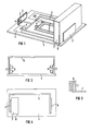
- the circuit carrier 1 shows an electrically insulating circuit carrier 1 with ribs 2 formed on its surface.
- the circuit carrier 1 and the ribs 2 have metallized tracks and surfaces 3.
- Components 4 arranged on the circuit carrier 1 are connected to these at least in part.
- the ribs 2 thus have the same function as the cooling ribs of heat sinks, but are an integral part of the circuit carrier 1 here. Particularly good heat dissipation is possible if the component 4 contacts the rib 2 over a large area and is, for example, attached directly to it.
- an assembly 7 can also have its outer cooling cap sel 8 made of sheet metal with a rib are connected over a large area.
- a heat-conducting plate 5, as shown in FIG. 4, can be attached to the same rib 2 in order to pass on the heat loss from the assembly 8.
- the heat is transported via the heat-conducting plate 5 to a further rib designed as a cooling element 9, which, for example according to FIG. 3, can also have a separate heat sink 6.
- the heat conducting sheet 5 connecting the two ribs 2 makes it possible to compensate for the heat between the two ribs 2, so that overheating of the components can be avoided.
- the one rib 2 serve once as a heat source and on the other hand as a heat sink with respect to the other rib 2, so that the heat transport direction will change accordingly.
- the heat-conducting plate 5 ensures that both ribs 2 are always involved in releasing the total power loss through all components 4 on the ribs 2 to the ambient air. Any combination of the features occurring in the figures is of course possible.
Abstract
Description
Die Erfindung betrifft einen elektrisch isolierenden Schaltungsträger mit von seiner Oberfläche abstehenden Elementen, die einstückig mit dem Schaltungsträger verbunden sind.The invention relates to an electrically insulating circuit carrier with elements protruding from its surface, which are integrally connected to the circuit carrier.
Aus der DE-OS 32 22 178 ist ein elektrisch isolierender Schaltungsträger, der einstückig mit Aufnahmen verbunden und mit diesen hergestellt ist, bekannt. Dieser Träger wird nachträglich im Heißprägeverfahren mit metallischen Leitern zur elektrischen Stromleitung versehen. Hierbei dienen starre Rippen, Stege, Stifte, Säulen oder Konsolen der Bauelementeaufnahme. Mit diesem Träger wird die Aufgabe gelöst, nicht nur die Verdrahtung, sondern auch die Montage elektrischer Bauelemente sowie mechanischer Baugruppen zu vereinfachen und zu rationalisieren. Hinweise auf eine hierin zu integrierende Kühlung der Bauelemente sind jedoch nicht angegeben.From DE-OS 32 22 178 an electrically insulating circuit carrier, which is integrally connected to receptacles and is produced with these, is known. This carrier is subsequently hot-stamped with metallic conductors for electrical power supply. Rigid ribs, webs, pins, columns or brackets are used to hold the components. This carrier solves the task of not only simplifying and rationalizing the wiring, but also the assembly of electrical components and mechanical assemblies. However, indications of a cooling of the components to be integrated are not given.
Weiterhin ist bekannt, zur Kühlung von Bauelementen auf einer Leiterplatte Kühlkörper zu verwenden. Die DE-OS 34 16 348 offenbart eine Leiterplatte mit einer Ausnehmung, durch die ein Zapfen eines Kühlkörpers geführt ist. Mit dem Zapfen wird ein auf der Leiterplatte angeordnetes, elektrisches Bauelement wärmeleitend verbunden. Die Verwendung eines Kühlkörpers als zusätzliches Element ist bekannt. Allerdings bedeutet der Zapfen an dem Kühlkörper als wärmeleitende Brücke zwischen dem Bauelement und dem eigentlichen Kühlkörper eine Vereinfachung.It is also known to use heat sinks for cooling components on a printed circuit board. DE-OS 34 16 348 discloses a printed circuit board with a recess through which a pin of a heat sink is guided. An electrical component arranged on the circuit board is connected in a heat-conducting manner to the pin. The use of a heat sink as an additional element is known. However, the pin on the heat sink as a heat-conducting bridge between the component and the actual heat sink means a simplification.
Hiervon ausgehend besteht die Aufgabe, bei elektrisch isolierenden Schaltungsträgern der obengenannten Art die Kühlung von auf dem Schaltungsträger angeordneten elektrischen Bauelementen mit guter Wirkung und durch einfache Bauweise zu verbessern. Dies wird dadurch gelöst, daß ein Teil der im wesentlichen flächig ausgebildeten Elemente metallisierte Bahnen und/oder Flächen aufweist, die zur Abführung und Weiterleitung der Verlustwärme durch auf dem Schaltungsträger angeordnete und in Betrieb befindliche elektrische Bauelemente dienen. Die Elemente sind zweckmäßigerweise als Rippen, Stege oder Zapfen ausgeführt. Besteht zwischen einem Teil der Bauelemente und der metallisierten Fläche eines Elements direkter Berührungskontakt, so ist die Abführung der Verlustwärme von den Bauelementen besonders wirksam. Eine vorteilhafte Ausführung ist gegeben, wenn ein Teil der metallisierten Elemente untereinander durch ein Wärmeleitblech miteinander verbunden ist, da ein solches Wärmeleitblech nicht nur eine gute Wärmebrücke darstellt, sondern auch nachträglich den räumlichen Gegebenheiten entsprechend geformt werden kann. Weiterhin ist es von Vorteil, wenn auf dem Schaltungsträger wenigstens eine Baugruppe elektrisch angeschlossen ist und diese mindestens ein metallisiertes Element großflächig zur Wärmeleitung kontaktiert und von diesem Element als Ort einer Wärmequelle eine Verbindung über wenigstens ein Wärmeleitblech zu anderen, als Wärmesenke dienenden Kühlelementen auf dem Schaltungsträger besteht, wobei die von den Kühlelementen aufgenommene Wärme an die Umgebungsluft abgestrahlt wird. Die auf diese Weise vorgenommene Kühlung der Baugruppe erweist sich als besonders einfach und wirksam. Es ist außerdem vorteilhaft, wenn die Kühlelemente integraler Bestandteil des Schaltungsträgers sind, z.B. in Form von angeformten Rippen, Stegen oder Zapfen. Derartige Kühlelemente werden, wie die zuvor schon genannten Elemente, in einem Arbeitsprozeß durch Spritzguß des Schaltungsträgers, z.B. einer Leiterplatte hergestellt und erfordern demgemäß einen weitaus geringeren Kostenaufwand wie z.B. eine Lösung mit zusätzlichen Kühlkörpern, die zudem noch montiert werden müssen. Um die Abführung von Verlustwärme aus Baugruppen mit z.B. Leiterplatten zu verbessern, ist es von Vorteil, wenn die Baugruppen nach außen jeweils eine Kühlkapsel aus Metallblech aufweisen, die das metallisierte Element auf dem Schaltungsträger großflächig berührt.Proceeding from this, the object is to improve the cooling of electrical components arranged on the circuit carrier with good effect and by simple construction in the case of electrically insulating circuit carriers of the type mentioned above. This is achieved in that some of the essentially flat elements have metallized tracks and / or surfaces which are used to dissipate and transfer the heat loss through electrical components arranged on the circuit carrier and in operation. The elements are expediently designed as ribs, webs or pins. If there is direct contact between part of the components and the metallized surface of an element, the dissipation of the heat loss from the components is particularly effective. An advantageous embodiment is provided if some of the metallized elements are connected to one another by a heat-conducting plate, since such a heat-conducting plate not only represents a good thermal bridge, but can also be shaped subsequently according to the spatial conditions. Furthermore, it is advantageous if at least one assembly is electrically connected to the circuit carrier and this contacts at least one metallized element over a large area for heat conduction and from this element as the location of a heat source a connection via at least one heat conducting plate to other cooling elements on the circuit carrier serving as a heat sink there, the heat absorbed by the cooling elements is radiated to the ambient air. The cooling of the assembly carried out in this way proves to be particularly simple and effective. It is also advantageous if the cooling elements are an integral part of the circuit carrier, e.g. in the form of molded ribs, webs or pins. Such cooling elements are, like the elements already mentioned, in one working process by injection molding the circuit carrier, e.g. a printed circuit board and accordingly require a much lower cost, such as a solution with additional heat sinks that also have to be installed. To remove heat loss from assemblies with e.g. To improve printed circuit boards, it is advantageous if the assemblies each have a cooling capsule made of sheet metal on the outside, which contacts the metallized element on the circuit carrier over a large area.
Ausführungsformen der Erfindung werden im folgenden anhand einer Zeichnung näher erläutert.Embodiments of the invention are explained in more detail below with reference to a drawing.
Es zeigen:
- FIG 1 einen elektrisch isolierenden Schaltungsträger in perspektivischer Darstellung,
- FIG 2 einen Querschnitt eines Schaltungsträgers mit Einsatz eines Wärmeleitbleches,
- FIG 3 eine Rippe als integraler Bestandteil eines Schaltungsträgers mit daran angebrachtem Kühlkörper,
- FIG 4 eine Draufsicht auf einen Schaltungsträger mit Stegen und einem Wärmeleitblech als Mittel zur Abführung von Verlustwärme einer Baugruppe.
- 1 shows an electrically insulating circuit carrier in a perspective view,
- 2 shows a cross section of a circuit carrier using a heat-conducting sheet,
- 3 shows a rib as an integral part of a circuit carrier with a heat sink attached to it,
- 4 shows a plan view of a circuit carrier with webs and a heat-conducting sheet as a means for dissipating heat loss from an assembly.
FIG 1 zeigt einen elektrisch isolierenden Schaltungsträger 1 mit an seiner Oberfläche angeformten Rippen 2. Der Schaltungsträger 1 und die Rippen 2 weisen metallisierte Bahnen und Flächen 3 auf. Mit diesen sind auf dem Schaltungsträger 1 angeordnete Bauelemente 4 wenigstens zum Teil verbunden. Dadurch wird die von den Bauelementen 4 erzeugte Verlustwärme über die Bahnen und Flächen 3, insbesondere auf den Rippen 2 abgeführt. Die Rippen 2 haben somit die gleiche Funktion wie die Kühlrippen von Kühlkörpern, sind jedoch hier integraler Bestandteil des Schaltungsträgers 1. Eine besonders gute Wärmeabführung ist möglich, wenn das Bauelement 4 die Rippe 2 großflächig kontaktiert und z.B. direkt auf ihr befestigt ist. Statt eines Bauelementes 4 kann aber auch eine Baugruppe 7 über ihre äußere Kühlkapsel 8 aus Metallblech mit einer Rippe großflächig in Verbindung stehen. Zur Weiterleitung der Verlustwärme der Baugruppe 8 kann an derselben Rippe 2 ein Wärmeleitblech 5 angebracht werden, wie es in FIG 4 dargestellt ist. Hier wird der Wärmetransport über das Wärmeleitblech 5 zu einer weiteren als Kühlelement 9 ausgebildeten Rippe vorgenommen, die z.B. gemäß FIG 3 zudem noch einen gesonderten Kühlkörper 6 aufweisen kann.1 shows an electrically insulating circuit carrier 1 with ribs 2 formed on its surface. The circuit carrier 1 and the ribs 2 have metallized tracks and
FIG 2 zeigt zwei an dem Schaltungsträger 1 angeformte Rippen 2, die metallisiert sind und an der Oberfläche Bauelemente 4 tragen. Abhängig vom Betrieb erzeugen die Bauelemente 4 unterschiedliche Verlustwärme. Durch das beide Rippen 2 verbindende Wärmeleitblech 5 ist ein Ausgleich der Wärme zwischen beiden Rippen 2 möglich, so daß eine Überhitzung der Bauelemente vermieden werden kann. Z.B. kann je nach Betriebsart, d.h. dem Anfall an Verlustwärme durch die Bauelemente 4 die eine Rippe 2 einmal als Wärmequelle und zum anderen als Wärmesenke gegenüber der anderen Rippe 2 dienen, so daß die Wärmetransportrichtung sich entsprechend ändern wird. Durch das Wärmeleitblech 5 wird erreicht, daß stets beide Rippen 2 an der Abgabe der gesamten Verlustleistung durch sämtliche Bauelemente 4 auf den Rippen 2 an die Umgebungsluft beteiligt sind. Selbstverständlich ist jede Kombination der bei den Figuren vorkommenden Merkmale möglich.2 shows two ribs 2 formed on the circuit carrier 1, which are metallized and have
Claims (7)
Priority Applications (2)
| Application Number | Priority Date | Filing Date | Title |
|---|---|---|---|
| DE90113092T DE59003026D1 (en) | 1990-07-09 | 1990-07-09 | Electrically insulating circuit carrier with integrated coolants. |
| EP19900113092 EP0465693B1 (en) | 1990-07-09 | 1990-07-09 | Electrical insulating printed circuit board with integrated cooling means |
Applications Claiming Priority (1)
| Application Number | Priority Date | Filing Date | Title |
|---|---|---|---|
| EP19900113092 EP0465693B1 (en) | 1990-07-09 | 1990-07-09 | Electrical insulating printed circuit board with integrated cooling means |
Publications (2)
| Publication Number | Publication Date |
|---|---|
| EP0465693A1 true EP0465693A1 (en) | 1992-01-15 |
| EP0465693B1 EP0465693B1 (en) | 1993-10-06 |
Family
ID=8204194
Family Applications (1)
| Application Number | Title | Priority Date | Filing Date |
|---|---|---|---|
| EP19900113092 Expired - Lifetime EP0465693B1 (en) | 1990-07-09 | 1990-07-09 | Electrical insulating printed circuit board with integrated cooling means |
Country Status (2)
| Country | Link |
|---|---|
| EP (1) | EP0465693B1 (en) |
| DE (1) | DE59003026D1 (en) |
Cited By (5)
| Publication number | Priority date | Publication date | Assignee | Title |
|---|---|---|---|---|
| EP0607845A1 (en) * | 1993-01-22 | 1994-07-27 | Siemens Aktiengesellschaft | One piece insulating part, especially injection molded part |
| EP0607846A1 (en) * | 1993-01-22 | 1994-07-27 | Siemens Aktiengesellschaft | One piece plastic part, especially injection molded part |
| US7298028B2 (en) | 2005-07-14 | 2007-11-20 | Via Technologies, Inc. | Printed circuit board for thermal dissipation and electronic device using the same |
| CN100361296C (en) * | 2005-08-22 | 2008-01-09 | 威盛电子股份有限公司 | Print circuit board with improved heat rejection structure and electronic device |
| WO2018134050A1 (en) * | 2017-01-23 | 2018-07-26 | Sma Solar Technology Ag | Relay arrangement with improved heat dissipation and converter device having a relay arrangement of this kind |
Citations (4)
| Publication number | Priority date | Publication date | Assignee | Title |
|---|---|---|---|---|
| DE3147789A1 (en) * | 1981-12-03 | 1983-06-09 | Brown, Boveri & Cie Ag, 6800 Mannheim | Power module and method of producing it |
| DE3416348A1 (en) * | 1984-05-03 | 1985-11-07 | Siemens AG, 1000 Berlin und 8000 München | Compact assembly in which a printed-circuit board is connected to a heat sink |
| GB2164499A (en) * | 1984-09-18 | 1986-03-19 | Howwood Ind Limited | Heat sinks for electronic components |
| US4811165A (en) * | 1987-12-07 | 1989-03-07 | Motorola, Inc. | Assembly for circuit modules |
-
1990
- 1990-07-09 EP EP19900113092 patent/EP0465693B1/en not_active Expired - Lifetime
- 1990-07-09 DE DE90113092T patent/DE59003026D1/en not_active Expired - Fee Related
Patent Citations (4)
| Publication number | Priority date | Publication date | Assignee | Title |
|---|---|---|---|---|
| DE3147789A1 (en) * | 1981-12-03 | 1983-06-09 | Brown, Boveri & Cie Ag, 6800 Mannheim | Power module and method of producing it |
| DE3416348A1 (en) * | 1984-05-03 | 1985-11-07 | Siemens AG, 1000 Berlin und 8000 München | Compact assembly in which a printed-circuit board is connected to a heat sink |
| GB2164499A (en) * | 1984-09-18 | 1986-03-19 | Howwood Ind Limited | Heat sinks for electronic components |
| US4811165A (en) * | 1987-12-07 | 1989-03-07 | Motorola, Inc. | Assembly for circuit modules |
Non-Patent Citations (1)
| Title |
|---|
| IBM TECHNICAL DISCLOSURE BULLETIN Band 28, Nr. 12, Mai 1986, Seiten 5565-5567, New York, US; "Ground plane thermal conduction brackets" * |
Cited By (11)
| Publication number | Priority date | Publication date | Assignee | Title |
|---|---|---|---|---|
| EP0607845A1 (en) * | 1993-01-22 | 1994-07-27 | Siemens Aktiengesellschaft | One piece insulating part, especially injection molded part |
| EP0607846A1 (en) * | 1993-01-22 | 1994-07-27 | Siemens Aktiengesellschaft | One piece plastic part, especially injection molded part |
| US5461201A (en) * | 1993-01-22 | 1995-10-24 | Siemens Aktiengesellschaft | Insulating part with integral cooling element |
| US5468909A (en) * | 1993-01-22 | 1995-11-21 | Siemens Aktiensesellschaft | Insulating part with improved heat transfer element |
| US7298028B2 (en) | 2005-07-14 | 2007-11-20 | Via Technologies, Inc. | Printed circuit board for thermal dissipation and electronic device using the same |
| CN100361296C (en) * | 2005-08-22 | 2008-01-09 | 威盛电子股份有限公司 | Print circuit board with improved heat rejection structure and electronic device |
| WO2018134050A1 (en) * | 2017-01-23 | 2018-07-26 | Sma Solar Technology Ag | Relay arrangement with improved heat dissipation and converter device having a relay arrangement of this kind |
| CN110199371A (en) * | 2017-01-23 | 2019-09-03 | 艾思玛太阳能技术股份公司 | Relay assembly with improved heat dissipation and the convertor device with the relay assembly |
| CN110199371B (en) * | 2017-01-23 | 2021-08-31 | 艾思玛太阳能技术股份公司 | Relay assembly with improved heat dissipation and inverter device having the same |
| US11129272B2 (en) | 2017-01-23 | 2021-09-21 | Sma Solar Technology Ag | Relay arrangement with improved heat dissipation and converter device having a relay arrangement of this kind |
| US11570884B2 (en) | 2017-01-23 | 2023-01-31 | Sma Solar Technology Ag | Relay arrangement with improved heat dissipation and converter device having a relay arrangement of this kind |
Also Published As
| Publication number | Publication date |
|---|---|
| DE59003026D1 (en) | 1993-11-11 |
| EP0465693B1 (en) | 1993-10-06 |
Similar Documents
| Publication | Publication Date | Title |
|---|---|---|
| DE10322745B4 (en) | Power semiconductor device with high radiation efficiency | |
| EP0847595B1 (en) | Cooling element for electronic components | |
| DE69532700T2 (en) | Control circuit module | |
| WO1994029901A1 (en) | Securing device for semiconductor circuit components | |
| DE4031051C2 (en) | Module with at least one semiconductor switching element and a control circuit | |
| DE102005057981A1 (en) | Power semiconductor device | |
| DE3123930A1 (en) | HEAT ARRESTER FOR A DUAL-IN-LINE HOUSING FOR INTEGRATED CIRCUITS | |
| DE112016004646B4 (en) | ELECTRICAL DISTRIBUTION BOX | |
| DE4422113C2 (en) | electronic module | |
| DE102014006360B4 (en) | Electrical circuit | |
| WO2010006924A1 (en) | Motor control device of a vehicle | |
| EP3763177B1 (en) | Electrical appliance arrangement having an electrical appliance which can be fastened to a support element, in particular a wall | |
| DE102018129418A1 (en) | circuitry | |
| DE69912657T2 (en) | Automotive switch box | |
| DE112019006498T5 (en) | Converter | |
| EP0674828A1 (en) | Device with a plastic substrate to accept and hold an electronic module. | |
| EP0465693B1 (en) | Electrical insulating printed circuit board with integrated cooling means | |
| DE3903615C2 (en) | ||
| DE202010017443U1 (en) | Electrical assembly | |
| DE102014109874A1 (en) | Electronic element and electronic device | |
| DE202020101852U1 (en) | Thermal interface for multiple discrete electronic devices | |
| DE19642405A1 (en) | Cooling device for electronic part, e.g. CPU | |
| EP1758165B1 (en) | Power semiconductor module with means for mounting on a heatsink | |
| DE112019002582T5 (en) | Switching device | |
| DE102020005363A1 (en) | Electrical device and method for producing a first and second electrical device from a kit |
Legal Events
| Date | Code | Title | Description |
|---|---|---|---|
| PUAI | Public reference made under article 153(3) epc to a published international application that has entered the european phase |
Free format text: ORIGINAL CODE: 0009012 |
|
| 17P | Request for examination filed |
Effective date: 19901205 |
|
| AK | Designated contracting states |
Kind code of ref document: A1 Designated state(s): CH DE FR GB IT LI SE |
|
| 17Q | First examination report despatched |
Effective date: 19930208 |
|
| GRAA | (expected) grant |
Free format text: ORIGINAL CODE: 0009210 |
|
| AK | Designated contracting states |
Kind code of ref document: B1 Designated state(s): CH DE FR GB IT LI SE |
|
| REF | Corresponds to: |
Ref document number: 59003026 Country of ref document: DE Date of ref document: 19931111 |
|
| ITF | It: translation for a ep patent filed |
Owner name: STUDIO JAUMANN |
|
| ET | Fr: translation filed | ||
| GBT | Gb: translation of ep patent filed (gb section 77(6)(a)/1977) |
Effective date: 19940106 |
|
| PG25 | Lapsed in a contracting state [announced via postgrant information from national office to epo] |
Ref country code: SE Effective date: 19940710 |
|
| PG25 | Lapsed in a contracting state [announced via postgrant information from national office to epo] |
Ref country code: LI Effective date: 19940731 Ref country code: CH Effective date: 19940731 |
|
| PLBE | No opposition filed within time limit |
Free format text: ORIGINAL CODE: 0009261 |
|
| STAA | Information on the status of an ep patent application or granted ep patent |
Free format text: STATUS: NO OPPOSITION FILED WITHIN TIME LIMIT |
|
| 26N | No opposition filed | ||
| EUG | Se: european patent has lapsed |
Ref document number: 90113092.2 Effective date: 19950210 |
|
| REG | Reference to a national code |
Ref country code: CH Ref legal event code: PL |
|
| EUG | Se: european patent has lapsed |
Ref document number: 90113092.2 |
|
| PGFP | Annual fee paid to national office [announced via postgrant information from national office to epo] |
Ref country code: GB Payment date: 19980623 Year of fee payment: 9 |
|
| PGFP | Annual fee paid to national office [announced via postgrant information from national office to epo] |
Ref country code: FR Payment date: 19980729 Year of fee payment: 9 |
|
| PG25 | Lapsed in a contracting state [announced via postgrant information from national office to epo] |
Ref country code: GB Free format text: LAPSE BECAUSE OF NON-PAYMENT OF DUE FEES Effective date: 19990709 |
|
| PG25 | Lapsed in a contracting state [announced via postgrant information from national office to epo] |
Ref country code: FR Free format text: THE PATENT HAS BEEN ANNULLED BY A DECISION OF A NATIONAL AUTHORITY Effective date: 19990731 |
|
| GBPC | Gb: european patent ceased through non-payment of renewal fee |
Effective date: 19990709 |
|
| REG | Reference to a national code |
Ref country code: FR Ref legal event code: ST |
|
| PGFP | Annual fee paid to national office [announced via postgrant information from national office to epo] |
Ref country code: DE Payment date: 20010919 Year of fee payment: 12 |
|
| PG25 | Lapsed in a contracting state [announced via postgrant information from national office to epo] |
Ref country code: DE Free format text: LAPSE BECAUSE OF NON-PAYMENT OF DUE FEES Effective date: 20030201 |
|
| PG25 | Lapsed in a contracting state [announced via postgrant information from national office to epo] |
Ref country code: IT Free format text: LAPSE BECAUSE OF NON-PAYMENT OF DUE FEES;WARNING: LAPSES OF ITALIAN PATENTS WITH EFFECTIVE DATE BEFORE 2007 MAY HAVE OCCURRED AT ANY TIME BEFORE 2007. THE CORRECT EFFECTIVE DATE MAY BE DIFFERENT FROM THE ONE RECORDED. Effective date: 20050709 |