EP0398741B1 - Image information transmitting system - Google Patents
Image information transmitting system Download PDFInfo
- Publication number
- EP0398741B1 EP0398741B1 EP90305399A EP90305399A EP0398741B1 EP 0398741 B1 EP0398741 B1 EP 0398741B1 EP 90305399 A EP90305399 A EP 90305399A EP 90305399 A EP90305399 A EP 90305399A EP 0398741 B1 EP0398741 B1 EP 0398741B1
- Authority
- EP
- European Patent Office
- Prior art keywords
- data
- block
- distribution
- pixel
- error
- Prior art date
- Legal status (The legal status is an assumption and is not a legal conclusion. Google has not performed a legal analysis and makes no representation as to the accuracy of the status listed.)
- Expired - Lifetime
Links
Images


Classifications
-
- H—ELECTRICITY
- H04—ELECTRIC COMMUNICATION TECHNIQUE
- H04N—PICTORIAL COMMUNICATION, e.g. TELEVISION
- H04N19/00—Methods or arrangements for coding, decoding, compressing or decompressing digital video signals
- H04N19/85—Methods or arrangements for coding, decoding, compressing or decompressing digital video signals using pre-processing or post-processing specially adapted for video compression
- H04N19/89—Methods or arrangements for coding, decoding, compressing or decompressing digital video signals using pre-processing or post-processing specially adapted for video compression involving methods or arrangements for detection of transmission errors at the decoder
- H04N19/895—Methods or arrangements for coding, decoding, compressing or decompressing digital video signals using pre-processing or post-processing specially adapted for video compression involving methods or arrangements for detection of transmission errors at the decoder in combination with error concealment
-
- H—ELECTRICITY
- H04—ELECTRIC COMMUNICATION TECHNIQUE
- H04N—PICTORIAL COMMUNICATION, e.g. TELEVISION
- H04N19/00—Methods or arrangements for coding, decoding, compressing or decompressing digital video signals
- H04N19/90—Methods or arrangements for coding, decoding, compressing or decompressing digital video signals using coding techniques not provided for in groups H04N19/10-H04N19/85, e.g. fractals
- H04N19/98—Adaptive-dynamic-range coding [ADRC]
Definitions
- the present invention relates to an image information transmitting system and, more particularly, to an image information transmitting system capable of performing high-efficiency coding.
- a high-efficiency coding scheme for a television signal is known as an image information transmitting scheme of this type.
- a so-called MIN-MAX method for reducing the average number of bits per pixel is employed. The MIN-MAX method will be described below.
- a television signal has strong correlation with time and space.
- the blocks When an image is divided into small blocks, the blocks often have only a small dynamic range due to local correlation.
- a local dynamic range is obtained in each block, and adaptive coding is performed to perform highly efficient data compression.
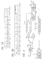
- Fig. 1 is a schematic block diagram of an image information transmitting system as a prior art.
- the image information transmitting system includes an input terminal 301.
- An analog signal obtained by raster-scanning, e.g., a television signal is sampled at a predetermined frequency, and data (n bits/sample) is input to the input terminal 301.
- the digital image data having 2 n gradation levels are supplied to a pixel block dividing circuit 302.
- Fig. 2 is a view showing a state wherein one-frame pixel data are divided into pixel blocks.
- the one-frame pixel data are temporarily stored in a memory or the like.
- the pixel data are read out in units of blocks each having (l x m) pixels, i.e., l pixels in the horizontal direction (to be referred to as an H direction hereinafter) and m pixels in the vertical direction (to be referred to as a V direction thereinafter). That is, the data are output in units of pixel blocks.
- Fig. 3 shows a format of each pixel block.
- This pixel block contains pixel data D 1,1 to D m,l .
- Image data output from the pixel block dividing circuit 302 are input to a MAX value detection circuit 303, a MIN value detection circuit 304, and a timing adjusting circuit 305.
- a pixel (D max ) having a MAX value and a pixel (D min ) having a MIN value are detected by and output from the detection circuits 303 and 304, respectively.
- the timing adjusting circuit 305 delays all the pixel data by a period required to cause the MAX and MIN value detection circuits 303 and 304 to detect the pixels D max and D min .
- the pixel data are sent to a divided value converting circuit 306 in units of pixel blocks in a predetermined order. For example, data are sent in an order of D 1,1 , D 2,1 , D 3,1 ,..., D m,1 , D 1,2 ,... D m,2 ,..., D 1,(l-1) ,... D m,(l-1) , D 1,l ,..., and D m,l in units of pixel blocks.
- All the pixel data (D 1,1 to D m,l ) and MAX and MIN values (D max and D min ) of each pixel block are input to the divided value converting circuit 306 and are compared with 2 k (where k is an integer smaller than n ) quantization levels between the values D max and D min , thereby obtaining k-bit division codes ( ⁇ 1,1 to ⁇ m,l ).
- the quantization state is shown in Fig. 4A.
- the division code ⁇ i,j is output as a k-bit binary code.
- the obtained k-bit division code ⁇ i,j and the n-bit values D max and D min are converted into serial data by parallel-to-serial (P-S) converters 307, 307', and 307", respectively.
- P-S parallel-to-serial
- One of the outputs from the P-S converters is selected by a data selector 308, thus obtaining serial data shown in Fig. 5A.
- the data output from the data selector 308 is added with a p-bit error correction code (Fig. 5B) by an error correction code adding circuit 309.
- the output from the error correction code adding circuit 309 is processed by a first-in first-out (FIFO) memory 310 along the time axis so as to obtain a predetermined data transmission rate.
- a synchronizing signal adding circuit 311 is added with a synchronizing signal by a synchronizing signal adding circuit 311.
- the obtained signal is sent out from an output terminal 312 onto a transmission line (a magnetic recording/reproducing system such as a VTR).
- the synchronizing signal is added in units of pixel blocks or every plurality of pixel blocks.
- the operation timings of the above circuits are determined on the basis of timing signals output from a timing control circuit 313.
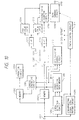
- Fig. 6 is a block diagram showing a schematic arrangement of a receiving side corresponding to a data transmitting side shown in Fig. 1.
- the receiving side in Fig. 6 includes an input terminal 821 for receiving transmission data highly efficiently coded at the transmitting side.
- the input transmission signal is supplied to a synchronizing signal separating circuit 822 and an error correction circuit 823.
- the synchronizing signal separating circuit 822 separates a synchronizing signal from the input transmission data and sends the separated synchronizing signal to the error correction circuit 823 and a timing control circuit 831.
- the error correction circuit 823 separates the error correction code from the transmission data in synchronism with the synchronizing signal supplied from the synchronizing signal separating circuit 822, detects a data error generated along the transmission line in accordance with the error correction code, corrects this error, and supplies the corrected data to a data selector 824.
- the timing control circuit 831 controls operating timings of the respective circuits on the receiving side on the basis of the synchronizing signal supplied from the synchronizing signal separating circuit 822.
- the data selector 824 separates the transmission data into the n-bit data D max and D min and the k-bit codes ⁇ i,j quantized between the values D max and D min . These separated data are supplied to serial-to-parallel (S-P) converters 825 and 825', respectively, and are converted into parallel data thereby.
- S-P serial-to-parallel
- the MAX and MIN value data D max and D min converted into the parallel data by the S-P converter 825 are latched by latch circuits 826 and 827, respectively.
- the latched MAX and MIN value data D max and D min are supplied to a divided value inverting circuit 828.
- the division code ⁇ i,j associated with all the pixel data in each pixel block are output from the S-P converter 825' in a predetermined order and are supplied to the divided value inverting converter 828.
- Fig. 4B is a view showing a state wherein representation data D i,j ' associated with the original pixel data are decoded from the division code ⁇ i,j and the MAX and MIN value data D max and D min .
- the representation value is set to be an intermediate value between the adjacent ones of 2 k quantization levels between the values D max and D min .
- the resultant n-bit representation value data (D 1,1 ' to D m,l ') from the divided value inverting circuit 828 are output in units of pixel blocks in the predetermined order.
- output data from the divided value inverting circuit 828 is converted in an order corresponding to raster scan, and the obtained data appears as decoded image data at an output terminal 830.
- the error correction code in order to correct a data error occurring on the transmission line, the error correction code must be added to the transmission data at the transmitting side, and the obtained data is sent onto the transmission line. At the receiving side, the data error occurring on the transmission line is corrected by using the error correction code. Redundancy of the transmission data is increased by the error correction code, and transmission efficiency cannot be improved much.
- the invention provides a method of transmitting image information, comprising:
- Embodiments of the invention illustrate various techniques for the replacing of erroneous data, such that image degradation can be minimised.
- the invention further provides a transmitting apparatus and a receiving apparatus suitable for implementing respective parts of the method of the invention, and also provides an image signal conveying image information transmitted in accordance with that method.
- Fig. 7A shows a schematic arrangement of a transmitting side of an image information transmitting system according to the first embodiment of the present invention.
- the same reference numerals as in Fig. 1 denote the same parts in Fig. 7A, and a detailed description thereof will be omitted.
- an error detection code adding circuit 101 adds q- and r-bit error detection codes to serial data output from a data selector 308a, and the obtained data are supplied to a FIFO memory 310, as shown in Fig. 7B.
- the error detection codes added by the error detection code adding circuit 101 are used to detect whether an error occurs in data.
- the number of bits of the error detection codes can be smaller than that of the error correction code, and redundancy of the transmission data can be reduced.
- Fig. 8 shows a schematic arrangement of a receiving side of the image information transmitting system according to the first embodiment of the present invention.
- the receiving side includes an input terminal 201 for receiving transmission data (Fig. 7B) coded with high efficiency by the transmitting side of Fig. 7A.
- the input transmission data is supplied to a data selector 202, an error detection circuit 203, and a synchronizing signal separating circuit 204.
- synchronizing signal separating circuit 204 a synchronizing signal is separated from the input transmission data, and the separated synchronizing signal is supplied to the error detection circuit 203 and a timing control circuit 205.
- the timing control circuit 205 controls operation timings of the respective circuits in the receiving side on the basis of the synchronizing signal supplied from the synchronizing signal separating circuit 204.
- the data selector 202 supplies the n-bit data D max to the A side, the n-bit data D min to the B side, and the k-bit code ⁇ i,j obtained by quantizing the data between the data D max and D min to the C side. These data are converted by serial-to-parallel (S-P) converters 206a, 206b, and 206c into parallel data, respectively.
- S-P serial-to-parallel
- the MAX value data D max of each pixel block which is converted into the parallel data by the S-P converter 206a is supplied to a memory 207a, and the B terminal of a data selector 208a.
- the MIN value data D min of each pixel block which is converted into the parallel data by the S-P converter 206b is supplied to a memory 207b and the B terminal of a data selector 208b.
- the division code ⁇ i,j associated with each pixel data within each pixel block and converted into the parallel data by the S-P converter 206c is supplied to a memory 207c and the B terminal of a data selector 208c.
- the memories 207a, 207b, and 207c are used to delay the input data by a one-field period each.
- the A terminals of the data selectors 208a, 208b, and 208c receive the MAX value data D max , the MIN value data D min , and the division code ⁇ i,j , respectively, of the immediately preceding field period.
- switching of the data selectors 208a, 208b, and 208c is controlled by an error detection result output from the error detection circuit 203. More specifically, when the error detection circuit 203 detects that no error occurs in the transmission data, the data selectors 208a to 208c are connected to the corresponding B terminals.
- the data selectors 208a and 208b are connected to the A terminals, respectively, and the data selector 208c is connected to the B terminal.
- the division code ⁇ i,j has an error, all the data selectors 208a to 208c are connected to the A side.
- the interpolation data is output from the data selector 208a, the data selector 208b, and/or the data selector 208c.
- the MAX value data D max , the MIN value data D min , and the division code ⁇ i,j respectively output from the data selectors 208a, 208b, and 208c are supplied to a divided value inverting circuit 211.
- the divided value inverting circuit 211 decodes the n-bit representation data D i,j associated with the original pixel data on the basis of the division code ⁇ i,j and the data D max and D min as in the receiving side shown in Fig. 6.
- the decoded data is supplied to a scan convert circuit 212.
- the scan convert circuit 212 converts the output data from the divided value inverting circuit 211 in an order corresponding to raster scan, and the converted data is output as decoded image data from an output terminal 213.
- the image data can be transmitted without its degradation.
- the transmission data of an immediately preceding field period stored in the memories 207a, 207b, and 207c can be transmitted to the divided value inverting circuit 211 as interpolation data in place of the data having the error.
- the present invention is not limited to this scheme.
- the transmission data of an immediately preceding field period, of transmission data which corresponds to an error, and transmission data corresponding to neighboring pixel blocks of a pixel block represented by the transmission data of the immediately preceding field period may be used to calculate interpolation data. With this arrangement, degradation of the image data can be minimized.
- Fig. 9A shows a schematic arrangement of a transmitting side of an image information transmitting system according to the second embodiment of the present invention.
- the same reference numerals as in Fig. 1 denote the same parts in Fig. 9A, and a detailed description thereof will be omitted.
- an error detection code adding circuit 101 adds q- and r-bit error detection codes to serial data output from a data selector 308a, and the obtained data are supplied to a FIFO memory 310, as shown in Fig. 9B.
- the error detection codes added by the error detection code adding circuit 101 are used to detect whether an error occurs in data.
- the number of bits of the error detection codes can be smaller than that of the error correction code, and redundancy of the transmission data can be reduced.
- Fig. 10 shows a schematic arrangement of a receiving side of the image information transmitting system according to the second embodiment of the present invention.
- the receiving side includes an input terminal 1201 for receiving transmission data (Fig. 9B) coded with high efficiency by the transmitting side of Fig. 9A.
- the input transmission data is supplied to memories 1202 and 1203, an error detection circuit 1204, and a synchronizing signal separating circuit 1205.
- the synchronizing signal separating circuit 1205 separates a synchronizing signal from the input transmission data and supplies the synchronizing signal to the error detection circuit 1204 and a timing control circuit 1217.
- the timing control circuit 1217 controls operation timings of the respective circuits on the receiving side on the basis of the synchronizing signal supplied from the synchronizing signal separating circuit 1205.
- the transmission data input from the input terminal 1201 are sequentially stored in the memories 1202 and 1203.
- the error detection circuit 1204 outputs error detection data representing that one of MAX value data D max , MIN value data D min , and a division code ⁇ i,j in the transmission data input from the input terminal 1201 has an error.
- the error detection data output from the error detection circuit 1204 is stored in an error detection data memory 1206.
- the transmission data corresponding to one-field image data is stored in the memories 1202 and 1203, and the error detection data corresponding to this transmission data is stored in the error detection data memory 1206.
- the data stored in the respective memories are then read out.
- new input transmission data and new error detection data are stored in the corresponding memory. Therefore, the memories store the new data in place of the readout data.
- the transmission data stored in the memory 1203 is read out in a FIFO order and supplied to the B terminal of a data selector 1207.
- an address generating circuit 1208 When the MAX value data D max or the MIN value data D min has an error, an address generating circuit 1208 outputs to the memory 1202 an address for reading out the data D max or D min in the transmission data corresponding to the neighboring pixel blocks on the screen in response to the error detection data supplied from the error detection data memory 1206.
- the address generating circuit 1208 When the division code ⁇ i,j has an error, the address generating circuit 1208 outputs to the memory 1202 an address for reading out the codes ⁇ i,j corresponding to the neighboring pixels in the pixel block.
- the stored data are read out from the memory 1202 in response to the read address output from the address generating circuit 1208.
- the readout data is supplied to an operation circuit 1209.
- the operation circuit 1209 calculates interpolation MAX value data D max ', interpolation MIN value data D min ', and an interpolation division code ⁇ i,j ' by using the data supplied from the memory 1202. The calculated data are supplied to the A terminal of the data selector 1207.
- the error detection data read out from the error detection data memory 1206 is also supplied to a data selector control circuit 1210.
- the data selector control circuit 1210 connects the data selector 1207 to the A terminal. Otherwise, the data selector control circuit 1210 connects the data selector 1207 to the B terminal.
- the data having an error is replaced with the corresponding interpolation data, and the interpolated data is output.
- the transmission data output from the data selector 1207 is separated into n-bit data D max and D min and the division code ⁇ i,j by a data selector 1211. These separated data are converted into parallel data by serial-to-parallel (S-P) converters 1212 and 1213.
- S-P serial-to-parallel
- the parallel MAX and MIN value data D max and D min from the S-P converter 1212 are latched by latches 1214 and 1215, respectively.
- the latched MAX and MIN value data D max and D min are supplied to a divided value inverting circuit 1216.
- the division code ⁇ i,j converted as parallel data by the S-P converter 1213 is also supplied to the divided value inverting circuit 1216.
- the divided value inverting circuit 1216 decodes n-bit representation data D i,j ' associated with the original pixel data on the basis of the division code ⁇ i,j and the data D max and D min as in the receiving side shown in Fig. 6.
- the decoded value is supplied to a scan convert circuit 1218.
- the scan convert circuit 1218 converts the output data from the divided value inverting circuit 1216 in an order corresponding to raster scan.
- the converted data is output as decoded image data from an output terminal 1219.
- the image data can be corrected to an extent that image quality degradation occurring on the transmission line is negligible. Since extra data is not transmitted, transmission efficiency can be improved.
- Fig. 11A shows a schematic arrangement of a transmitting side of an image information transmitting system according to the third embodiment of the present invention.
- the same reference numerals as in Fig. 1 denote the same parts in Fig. 11A, and a detailed description thereof will be omitted.
- an error detection code adding circuit 101 adds q- and r-bit error detection codes to serial data output from a data selector 308a, and the obtained data are supplied to a FIFO memory 310, as shown in Fig. 11B.
- the error detection codes added by the error detection code adding circuit 101 are used to detect whether an error occurs in data.
- the number of bits of the error detection codes can be smaller than that of the error correction code, and redundancy of the transmission data can be reduced.
- Fig. 12 shows a schematic arrangement of a receiving side of the image information transmitting system according to the third embodiment of the present invention.
- the receiving side includes an input terminal 2201 for receiving transmission data (Fig. 11B) coded with high efficiency by the transmitting side of Fig. 11A.
- the input transmission data is supplied to a data selector 2202, an error detection circuit 2203, and a synchronizing signal separating circuit 2204.
- synchronizing signal separating circuit 2204 a synchronizing signal is separated from the input transmission data, and the separated synchronizing signal is supplied to the error detection circuit 2203 and a timing control circuit 2205.
- the timing control circuit 2205 controls operation timings of the respective circuits in the receiving side on the basis of the synchronizing signal supplied from the synchronizing signal separating circuit 2204.
- the data selector 2202 supplies the n-bit data D max to the A side, the n-bit data D min to the B side, and the k-bit code ⁇ i,j obtained by quantizing the data between the data D max and D min to the C side. These data are converted by serial-to-parallel (S-P) converters 2206a, 2206b, and 2206c into parallel data, respectively.
- S-P serial-to-parallel
- the MAX value data D max of each pixel block which is converted into the parallel data by the S-P converter 2206a is supplied to a memory 2207a and the B terminal of a data selector 2208a.
- the MIN value data D min of each pixel block which is converted into the parallel data by the S-P converter 2206b is supplied to a memory 2207b and the B terminal of a data selector 2208b.
- the division code ⁇ i,j associated with each pixel data within each pixel block and converted into the parallel data by the S-P converter 2206c is supplied to a memory 2207c, the B terminal of a data selector 2208c, and an operation circuit 2209.
- the memories 2207a, 2207b, and 2207c are used to delay the input data by a one-field period each.
- the A terminals of the data selectors 2208a, 2208b, and 2208c receive the MAX value data D max , the MIN value data D min , and the division code ⁇ i,j , respectively.
- the operation circuit 2209 is a circuit for calculating an average value of the division codes ⁇ i,j associated with the pixel data of the pixel blocks output from the S-P converter 2206c.
- the data calculated by the operation circuit 2209 is supplied to the C terminal of the data selector 2208c, and a fixed data generator 2210 generates data representing an intermediate value of the values represented by the division codes ⁇ i,j .
- the output from the fixed data generator 2210 is supplied to the D terminal of the data selector 2208c.
- switching of the data selectors 2208a, 2208b, and 2208c is controlled by an error detection result output from the error detection circuit 2203. More specifically, when the error detection circuit 2203 detects that no error occurs in the transmission data, the data selectors 2208a to 2208c are connected to the corresponding B terminals. When only the MAX value data D max has an error, the data selector 2208a is connected to the A terminal. When only the MIN value data D min has an error, the data selector 2208b is connected to the A terminal. When the MIN and MIN value data D max and D min and the division code ⁇ i,j have errors, all the data selectors 2208a to 2208c are connected to the A side.
- the data selector 2208c when no error is present in the MAX data D max and the MIN value data D min , and an error is present in the division code ⁇ i,j , the data selector 2208c is connected to the C or D terminal in accordance with an error rate. More specifically, when the error detection circuit 2203 detects that the number of errors in the division codes ⁇ i,j exceeds a predetermined number, the average value of the division codes ⁇ i,j cannot be calculated. In this case, the data selector 2208c is connected to the D terminal, and data representing an intermediate value of the values of the division codes ⁇ i,j is output from the data selector 2208c in place of the data representing the average value.
- the error detection circuit 2203 detects that the detected number of errors in the division codes ⁇ i,j is smaller than the predetermined number
- the data selector 2208c is connected to the C terminal.
- Data representing the average value of the division codes ⁇ i,j and calculated by the operation circuit 2209 is output from the data selector 2208c.
- the data selectors 2208a, 2208b, and 2208c output the corresponding interpolation data in place of the error data.
- the MAX value data D max , the MIN value data D min , and the division code ⁇ i,j respectively output from the data selectors 2208a, 2208b, and 2208c are supplied to a divided value inverting circuit 2211.
- the divided value inverting circuit 2211 decodes n-bit representation value data D i,j associated from the original pixel data on the basis of the division code ⁇ i,j and the data D max and D min as in the receiving side shown in Fig. 6.
- the decoded data is supplied to a scan convert circuit 2212.
- the scan convert circuit 2211 converts the output data from the divided value inverting circuit 2211 in an order corresponding to raster scan.
- the converted data is output as decoded image data from an output terminal 2213.
Description
- The present invention relates to an image information transmitting system and, more particularly, to an image information transmitting system capable of performing high-efficiency coding.
- For example, a high-efficiency coding scheme for a television signal is known as an image information transmitting scheme of this type. In this high-efficiency coding scheme for the television signal, since a transmission band must be narrowed, a so-called MIN-MAX method for reducing the average number of bits per pixel is employed. The MIN-MAX method will be described below.
- A television signal has strong correlation with time and space. When an image is divided into small blocks, the blocks often have only a small dynamic range due to local correlation. A local dynamic range is obtained in each block, and adaptive coding is performed to perform highly efficient data compression.
- This coding scheme will be described in detail with reference to the accompanying drawings.
- Fig. 1 is a schematic block diagram of an image information transmitting system as a prior art. The image information transmitting system includes an
input terminal 301. An analog signal obtained by raster-scanning, e.g., a television signal is sampled at a predetermined frequency, and data (n bits/sample) is input to theinput terminal 301. The digital image data having 2n gradation levels are supplied to a pixelblock dividing circuit 302. - Fig. 2 is a view showing a state wherein one-frame pixel data are divided into pixel blocks. In the pixel
block dividing circuit 302, the one-frame pixel data are temporarily stored in a memory or the like. As shown in Fig. 2, the pixel data are read out in units of blocks each having (ℓ x m) pixels, i.e., ℓ pixels in the horizontal direction (to be referred to as an H direction hereinafter) and m pixels in the vertical direction (to be referred to as a V direction thereinafter). That is, the data are output in units of pixel blocks. - Fig. 3 shows a format of each pixel block. This pixel block contains pixel data D1,1 to Dm,ℓ. Image data output from the pixel
block dividing circuit 302 are input to a MAXvalue detection circuit 303, a MINvalue detection circuit 304, and atiming adjusting circuit 305. Of all the pixel data (D1,1 to Dm,ℓ ) in each pixel block, a pixel (Dmax) having a MAX value and a pixel (Dmin) having a MIN value are detected by and output from thedetection circuits - The timing adjusting
circuit 305 delays all the pixel data by a period required to cause the MAX and MINvalue detection circuits value converting circuit 306 in units of pixel blocks in a predetermined order. For example, data are sent in an order of D1,1, D2,1, D3,1,..., Dm,1, D1,2,... Dm,2,..., D1,(ℓ-1),... Dm,(ℓ-1), D1,ℓ,..., and Dm,ℓ in units of pixel blocks. - All the pixel data (D1,1 to Dm,ℓ) and MAX and MIN values (Dmax and Dmin) of each pixel block are input to the divided
value converting circuit 306 and are compared with 2k (where k is an integer smaller than n) quantization levels between the values Dmax and Dmin, thereby obtaining k-bit division codes (Δ1,1 to Δm,ℓ ). The quantization state is shown in Fig. 4A. - As shown in Fig. 4A, the division code Δi,j is output as a k-bit binary code. The obtained k-bit division code Δi,j and the n-bit values Dmax and Dmin are converted into serial data by parallel-to-serial (P-S)
converters data selector 308, thus obtaining serial data shown in Fig. 5A. The data output from thedata selector 308 is added with a p-bit error correction code (Fig. 5B) by an error correctioncode adding circuit 309. The output from the error correctioncode adding circuit 309 is processed by a first-in first-out (FIFO)memory 310 along the time axis so as to obtain a predetermined data transmission rate. In addition, an output from theFIFO memory 310 is added with a synchronizing signal by a synchronizingsignal adding circuit 311. The obtained signal is sent out from anoutput terminal 312 onto a transmission line (a magnetic recording/reproducing system such as a VTR). - The synchronizing signal is added in units of pixel blocks or every plurality of pixel blocks. The operation timings of the above circuits are determined on the basis of timing signals output from a timing control circuit 313.
- Fig. 6 is a block diagram showing a schematic arrangement of a receiving side corresponding to a data transmitting side shown in Fig. 1. The receiving side in Fig. 6 includes an
input terminal 821 for receiving transmission data highly efficiently coded at the transmitting side. The input transmission signal is supplied to a synchronizingsignal separating circuit 822 and anerror correction circuit 823. - The synchronizing
signal separating circuit 822 separates a synchronizing signal from the input transmission data and sends the separated synchronizing signal to theerror correction circuit 823 and atiming control circuit 831. - The
error correction circuit 823 separates the error correction code from the transmission data in synchronism with the synchronizing signal supplied from the synchronizingsignal separating circuit 822, detects a data error generated along the transmission line in accordance with the error correction code, corrects this error, and supplies the corrected data to adata selector 824. - The
timing control circuit 831 controls operating timings of the respective circuits on the receiving side on the basis of the synchronizing signal supplied from the synchronizingsignal separating circuit 822. - The
data selector 824 separates the transmission data into the n-bit data Dmax and Dmin and the k-bit codes Δi,j quantized between the values Dmax and Dmin. These separated data are supplied to serial-to-parallel (S-P)converters 825 and 825', respectively, and are converted into parallel data thereby. The MAX and MIN value data Dmax and Dmin converted into the parallel data by theS-P converter 825 are latched bylatch circuits value inverting circuit 828. The division code Δi,j associated with all the pixel data in each pixel block are output from the S-P converter 825' in a predetermined order and are supplied to the dividedvalue inverting converter 828. - Fig. 4B is a view showing a state wherein representation data D i,j' associated with the original pixel data are decoded from the division code Δi,j and the MAX and MIN value data Dmax and Dmin. As shown in Fig. 4B, the representation value is set to be an intermediate value between the adjacent ones of 2k quantization levels between the values Dmax and Dmin. The resultant n-bit representation value data (D1,1' to Dm,ℓ') from the divided
value inverting circuit 828 are output in units of pixel blocks in the predetermined order. In ascan convert circuit 829, output data from the dividedvalue inverting circuit 828 is converted in an order corresponding to raster scan, and the obtained data appears as decoded image data at anoutput terminal 830. - In the conventional arrangement, however, in order to correct a data error occurring on the transmission line, the error correction code must be added to the transmission data at the transmitting side, and the obtained data is sent onto the transmission line. At the receiving side, the data error occurring on the transmission line is corrected by using the error correction code. Redundancy of the transmission data is increased by the error correction code, and transmission efficiency cannot be improved much.
- A known system incorporating error correction as described above is disclosed for example in US-A-4 703 352 of Sony Corporation. Examples are described therein in which error correction capability can be provided independently for the MIN/MAX data and the pixel codes, or for the MIN/MAX data only. Another document US-A-4 792 953 of Ampex Corporation describes a system for digitally encoding a television signal, which includes operations of error correction and error concealment.
- The invention provides a method of transmitting image information, comprising:
- (a) dividing a plurality of pixel data comprising one image frame into a plurality of pixel data blocks, each block representing a predetermined number of pixels;
- (b) forming, for each pixel data block, distribution data representing a distribution of the pixel data of the pixel data block and position data representing for each pixel of the block a relative position in the distribution represented by said distribution data;
- (c) transmitting for each block via a transmission channel: (i) the distribution data; (ii) the position data and (iii) error detecting data for use in detecting whether an error occurs in the transmission channel; and
- (d) receiving for each block the distribution data, the position data and the error detecting data transmitted via the transmission channel;
- (e) detecting whether an error occurs in the received data for a given block by using the received error detecting data; and
- (f) replacing detected erroneous data of the received data using other data, in response to the detection of the occurrence of the error,
- wherein said detecting step (e) discriminates for each block between errors occurring in the distribution data and errors occurring in the position data, and wherein the replacing step (f) is performed in a manner dependent on the result of said discrimination, and
- wherein said error detection data is sufficient for the detection, but not the correction, of errors occurring each of the distribution data and the position data.
- In view of the fact that the error detection codes added for transmission are sufficient for error detection but not error correction, the advantages of data compression provided by the block based encoding of distribution data and position data can be maintained. Embodiments of the invention illustrate various techniques for the replacing of erroneous data, such that image degradation can be minimised.
- The invention further provides a transmitting apparatus and a receiving apparatus suitable for implementing respective parts of the method of the invention, and also provides an image signal conveying image information transmitted in accordance with that method.
- The above and other features and advantages of the present invention will be apparent from the detailed description of particular embodiments, which follows. These embodiments are presented by way of example only.
- Fig. 1 is a schematic block diagram of a transmitting side in a conventional image information transmitting system;
- Fig. 2 is a view showing a state wherein all pixel data are divided into pixel blocks;
- Fig. 3 is a view showing data layout of each pixel block;
- Fig. 4A is a view showing conversion characteristics of a divided value converting circuit shown in Fig. 1;
- Fig. 4B is a view showing conversion characteristics of a divided value inverting circuit shown in Fig. 6 (to be described later);
- Fig. 5A is a view showing a data string output from a
data selector 308 shown in Fig. 1; - Fig. 5B is a view showing a transmission data string output from the transmitting system shown in Fig. 1;
- Fig. 6 is a schematic block diagram of a receiving side corresponding to the transmitting side of the image information transmitting system shown in Fig. 1;
- Fig. 7A is a schematic block diagram of a transmitting side of an image information transmitting system according to the first embodiment of the present invention;
- Fig. 7B is a view showing a transmission data string output from the transmitting side shown in Fig. 7A;
- Fig. 8 is a schematic block diagram of a receiving side of the image information transmitting system according to the first embodiment of to the present invention;
- Fig. 9A is a schematic block diagram of a transmitting side of an image information transmitting system according to the second embodiment of the present invention;
- Fig. 9B is a view showing a transmission data string output from the transmitting side shown in Fig. 9A;
- Fig. 10 is a schematic block diagram of a receiving side of the image information transmitting system according to the second embodiment of the present invention;
- Fig. 11A is a schematic block diagram of a transmitting side of an image information transmitting system according to the third embodiment of the present invention;
- Fig. 11B is a view showing a transmission data string output from the transmitting side shown in Fig. 11A; and
- Fig. 12 is a schematic block diagram of a receiving side of the image information transmitting system according to the third embodiment of the present invention.
- The present invention will be described in detail with reference to the preferred embodiments hereinafter.
- Fig. 7A shows a schematic arrangement of a transmitting side of an image information transmitting system according to the first embodiment of the present invention. The same reference numerals as in Fig. 1 denote the same parts in Fig. 7A, and a detailed description thereof will be omitted.
- In this transmitting side shown in Fig. 7A, unlike the transmitting side shown in Fig. 1, an error detection
code adding circuit 101 adds q- and r-bit error detection codes to serial data output from adata selector 308a, and the obtained data are supplied to aFIFO memory 310, as shown in Fig. 7B. - With the above arrangement, the error detection codes added by the error detection
code adding circuit 101 are used to detect whether an error occurs in data. The number of bits of the error detection codes can be smaller than that of the error correction code, and redundancy of the transmission data can be reduced. - Fig. 8 shows a schematic arrangement of a receiving side of the image information transmitting system according to the first embodiment of the present invention.
- Referring to Fig. 8, the receiving side includes an
input terminal 201 for receiving transmission data (Fig. 7B) coded with high efficiency by the transmitting side of Fig. 7A. The input transmission data is supplied to a data selector 202, anerror detection circuit 203, and a synchronizingsignal separating circuit 204. - In the synchronizing
signal separating circuit 204, a synchronizing signal is separated from the input transmission data, and the separated synchronizing signal is supplied to theerror detection circuit 203 and atiming control circuit 205. - The
timing control circuit 205 controls operation timings of the respective circuits in the receiving side on the basis of the synchronizing signal supplied from the synchronizingsignal separating circuit 204. The data selector 202 supplies the n-bit data Dmax to the A side, the n-bit data Dmin to the B side, and the k-bit code Δi,j obtained by quantizing the data between the data Dmax and Dmin to the C side. These data are converted by serial-to-parallel (S-P)converters - The MAX value data Dmax of each pixel block which is converted into the parallel data by the
S-P converter 206a is supplied to amemory 207a, and the B terminal of adata selector 208a. - The MIN value data Dmin of each pixel block which is converted into the parallel data by the
S-P converter 206b is supplied to amemory 207b and the B terminal of adata selector 208b. - The division code Δi,j associated with each pixel data within each pixel block and converted into the parallel data by the
S-P converter 206c is supplied to amemory 207c and the B terminal of adata selector 208c. - The
memories data selectors - Note that switching of the
data selectors error detection circuit 203. More specifically, when theerror detection circuit 203 detects that no error occurs in the transmission data, thedata selectors 208a to 208c are connected to the corresponding B terminals. - When both the MAX and MIN value data Dmax and Dmin have errors, the
data selectors data selector 208c is connected to the B terminal. When the division code Δi,j has an error, all thedata selectors 208a to 208c are connected to the A side. - In the above operation, when an error occurs in the transmission data, the interpolation data is output from the
data selector 208a, thedata selector 208b, and/or thedata selector 208c. The MAX value data Dmax, the MIN value data Dmin, and the division code Δi,j respectively output from thedata selectors value inverting circuit 211. The dividedvalue inverting circuit 211 decodes the n-bit representation data Di,j associated with the original pixel data on the basis of the division code Δi,j and the data Dmax and Dmin as in the receiving side shown in Fig. 6. The decoded data is supplied to ascan convert circuit 212. Thescan convert circuit 212 converts the output data from the dividedvalue inverting circuit 211 in an order corresponding to raster scan, and the converted data is output as decoded image data from anoutput terminal 213. - As described above, even if data having high redundancy such as an error correction code need not be added to image data during its transmission, the image data can be transmitted without its degradation.
- In this embodiment, when an error occurs in the MAX value data Dmax, the MIN value data Dmin, and/or the division code Δi,j in the transmission data, the transmission data of an immediately preceding field period stored in the
memories value inverting circuit 211 as interpolation data in place of the data having the error. However, the present invention is not limited to this scheme. For example, the transmission data of an immediately preceding field period, of transmission data which corresponds to an error, and transmission data corresponding to neighboring pixel blocks of a pixel block represented by the transmission data of the immediately preceding field period may be used to calculate interpolation data. With this arrangement, degradation of the image data can be minimized. - As described above, according to this embodiment, there is provided a method and system for efficiently transmitting high-quality image information.
- The second embodiment of the present invention will be described below.
- Fig. 9A shows a schematic arrangement of a transmitting side of an image information transmitting system according to the second embodiment of the present invention. The same reference numerals as in Fig. 1 denote the same parts in Fig. 9A, and a detailed description thereof will be omitted.
- In this transmitting side shown in Fig. 9A, unlike the transmitting side shown in Fig. 1, an error detection
code adding circuit 101 adds q- and r-bit error detection codes to serial data output from adata selector 308a, and the obtained data are supplied to aFIFO memory 310, as shown in Fig. 9B. - With the above arrangement, the error detection codes added by the error detection
code adding circuit 101 are used to detect whether an error occurs in data. The number of bits of the error detection codes can be smaller than that of the error correction code, and redundancy of the transmission data can be reduced. - Fig. 10 shows a schematic arrangement of a receiving side of the image information transmitting system according to the second embodiment of the present invention.
- Referring to Fig. 10, the receiving side includes an
input terminal 1201 for receiving transmission data (Fig. 9B) coded with high efficiency by the transmitting side of Fig. 9A. The input transmission data is supplied tomemories error detection circuit 1204, and a synchronizingsignal separating circuit 1205. - The synchronizing
signal separating circuit 1205 separates a synchronizing signal from the input transmission data and supplies the synchronizing signal to theerror detection circuit 1204 and atiming control circuit 1217. - The
timing control circuit 1217 controls operation timings of the respective circuits on the receiving side on the basis of the synchronizing signal supplied from the synchronizingsignal separating circuit 1205. - The transmission data input from the
input terminal 1201 are sequentially stored in thememories error detection circuit 1204 outputs error detection data representing that one of MAX value data Dmax, MIN value data Dmin, and a division code Δi,j in the transmission data input from theinput terminal 1201 has an error. The error detection data output from theerror detection circuit 1204 is stored in an errordetection data memory 1206. - As described above, the transmission data corresponding to one-field image data is stored in the
memories detection data memory 1206. The data stored in the respective memories are then read out. During read access of each memory, new input transmission data and new error detection data are stored in the corresponding memory. Therefore, the memories store the new data in place of the readout data. - The transmission data stored in the
memory 1203 is read out in a FIFO order and supplied to the B terminal of adata selector 1207. - When the MAX value data Dmax or the MIN value data Dmin has an error, an
address generating circuit 1208 outputs to thememory 1202 an address for reading out the data Dmax or Dmin in the transmission data corresponding to the neighboring pixel blocks on the screen in response to the error detection data supplied from the errordetection data memory 1206. When the division code Δi,j has an error, theaddress generating circuit 1208 outputs to thememory 1202 an address for reading out the codes Δi,j corresponding to the neighboring pixels in the pixel block. The stored data are read out from thememory 1202 in response to the read address output from theaddress generating circuit 1208. The readout data is supplied to anoperation circuit 1209. - The
operation circuit 1209 calculates interpolation MAX value data Dmax', interpolation MIN value data Dmin', and an interpolation division code Δi,j' by using the data supplied from thememory 1202. The calculated data are supplied to the A terminal of thedata selector 1207. - The error detection data read out from the error
detection data memory 1206 is also supplied to a dataselector control circuit 1210. When a data error is represented by the input error detection data, the dataselector control circuit 1210 connects thedata selector 1207 to the A terminal. Otherwise, the dataselector control circuit 1210 connects thedata selector 1207 to the B terminal. When an error is present in the transmission data read out from thememory 1203, the data having an error is replaced with the corresponding interpolation data, and the interpolated data is output. - The transmission data output from the
data selector 1207 is separated into n-bit data Dmax and Dmin and the division code Δi,j by adata selector 1211. These separated data are converted into parallel data by serial-to-parallel (S-P)converters - The parallel MAX and MIN value data Dmax and Dmin from the
S-P converter 1212 are latched bylatches value inverting circuit 1216. - The division code Δi,j converted as parallel data by the
S-P converter 1213 is also supplied to the dividedvalue inverting circuit 1216. - The divided
value inverting circuit 1216 decodes n-bit representation data Di,j' associated with the original pixel data on the basis of the division code Δi,j and the data Dmax and Dmin as in the receiving side shown in Fig. 6. The decoded value is supplied to ascan convert circuit 1218. Thescan convert circuit 1218 converts the output data from the dividedvalue inverting circuit 1216 in an order corresponding to raster scan. The converted data is output as decoded image data from anoutput terminal 1219. - As described above, without adding data having high redundancy such as an error correction code to image signal during its transmission, the image data can be corrected to an extent that image quality degradation occurring on the transmission line is negligible. Since extra data is not transmitted, transmission efficiency can be improved.
- As described above, according to this embodiment, there is provided a method and system for efficiently transmitting high-quality image information.
- The third embodiment of the present invention will be described below.
- Fig. 11A shows a schematic arrangement of a transmitting side of an image information transmitting system according to the third embodiment of the present invention. The same reference numerals as in Fig. 1 denote the same parts in Fig. 11A, and a detailed description thereof will be omitted.
- In this transmitting side shown in Fig. 11A, unlike the transmitting side shown in Fig. 1, an error detection
code adding circuit 101 adds q- and r-bit error detection codes to serial data output from adata selector 308a, and the obtained data are supplied to aFIFO memory 310, as shown in Fig. 11B. - With the above arrangement, the error detection codes added by the error detection
code adding circuit 101 are used to detect whether an error occurs in data. The number of bits of the error detection codes can be smaller than that of the error correction code, and redundancy of the transmission data can be reduced. - Fig. 12 shows a schematic arrangement of a receiving side of the image information transmitting system according to the third embodiment of the present invention.
- Referring to Fig. 12, the receiving side includes an
input terminal 2201 for receiving transmission data (Fig. 11B) coded with high efficiency by the transmitting side of Fig. 11A. The input transmission data is supplied to adata selector 2202, anerror detection circuit 2203, and a synchronizingsignal separating circuit 2204. - In the synchronizing
signal separating circuit 2204, a synchronizing signal is separated from the input transmission data, and the separated synchronizing signal is supplied to theerror detection circuit 2203 and atiming control circuit 2205. - The
timing control circuit 2205 controls operation timings of the respective circuits in the receiving side on the basis of the synchronizing signal supplied from the synchronizingsignal separating circuit 2204. Thedata selector 2202 supplies the n-bit data Dmax to the A side, the n-bit data Dmin to the B side, and the k-bit code Δi,j obtained by quantizing the data between the data Dmax and Dmin to the C side. These data are converted by serial-to-parallel (S-P)converters - The MAX value data Dmax of each pixel block which is converted into the parallel data by the
S-P converter 2206a is supplied to amemory 2207a and the B terminal of adata selector 2208a. The MIN value data Dmin of each pixel block which is converted into the parallel data by theS-P converter 2206b is supplied to amemory 2207b and the B terminal of adata selector 2208b. The division code Δi,j associated with each pixel data within each pixel block and converted into the parallel data by theS-P converter 2206c is supplied to amemory 2207c, the B terminal of adata selector 2208c, and anoperation circuit 2209. - The
memories data selectors - The
operation circuit 2209 is a circuit for calculating an average value of the division codes Δi,j associated with the pixel data of the pixel blocks output from theS-P converter 2206c. The data calculated by theoperation circuit 2209 is supplied to the C terminal of thedata selector 2208c, and a fixeddata generator 2210 generates data representing an intermediate value of the values represented by the division codes Δi,j. The output from the fixeddata generator 2210 is supplied to the D terminal of thedata selector 2208c. - Note that switching of the
data selectors error detection circuit 2203. More specifically, when theerror detection circuit 2203 detects that no error occurs in the transmission data, thedata selectors 2208a to 2208c are connected to the corresponding B terminals. When only the MAX value data Dmax has an error, thedata selector 2208a is connected to the A terminal. When only the MIN value data Dmin has an error, thedata selector 2208b is connected to the A terminal. When the MIN and MIN value data Dmax and Dmin and the division code Δi,j have errors, all thedata selectors 2208a to 2208c are connected to the A side. - In this embodiment, when no error is present in the MAX data Dmax and the MIN value data Dmin, and an error is present in the division code Δi,j, the
data selector 2208c is connected to the C or D terminal in accordance with an error rate. More specifically, when theerror detection circuit 2203 detects that the number of errors in the division codes Δi,j exceeds a predetermined number, the average value of the division codes Δi,j cannot be calculated. In this case, thedata selector 2208c is connected to the D terminal, and data representing an intermediate value of the values of the division codes Δi,j is output from thedata selector 2208c in place of the data representing the average value. However, when theerror detection circuit 2203 detects that the detected number of errors in the division codes Δi,j is smaller than the predetermined number, thedata selector 2208c is connected to the C terminal. Data representing the average value of the division codes Δi,j and calculated by theoperation circuit 2209 is output from thedata selector 2208c. - In the above operation, when an error occurs in the transmission data, the
data selectors data selectors value inverting circuit 2211. The dividedvalue inverting circuit 2211 decodes n-bit representation value data Di,j associated from the original pixel data on the basis of the division code Δi,j and the data Dmax and Dmin as in the receiving side shown in Fig. 6. The decoded data is supplied to ascan convert circuit 2212. - The
scan convert circuit 2211 converts the output data from the dividedvalue inverting circuit 2211 in an order corresponding to raster scan. The converted data is output as decoded image data from anoutput terminal 2213. - As described above, even if data having high redundancy such as an error correction code is not added to image data during its transmission, various types of interpolation data can be formed in accordance with the error rate of the image data, and the data having an error is interpolated with the interpolation data. Therefore, the image data can be transmitted without being degraded.
- As described above, according to this embodiment, there is provided a method and system for efficiently transmitting high-quality image information.
Claims (14)
- A method of transmitting image information, comprising:(a) dividing (302) a plurality of pixel data comprising one image frame into a plurality of pixel data blocks, each block representing a predetermined number (l x m) of pixels;(b) forming (304-306), for each pixel data block, distribution data (Dmin, Dmax) representing a distribution of the pixel data of the pixel data block and position data (Δi,j) representing for each pixel of the block a relative position in the distribution represented by said distribution data;(c) transmitting (307-312) for each block via a transmission channel: (i) the distribution data; (ii) the position data and (iii) error detecting data for use in detecting whether an error occurs in the transmission channel;(d) receiving (201-206) for each block the distribution data, the position data and the error detecting data transmitted via the transmission channel;(e) detecting (203) whether an error occurs in the received data for a given block by using the received error detecting data; and(f) replacing (208a-208c) detected erroneous data of the received data using other data (A), in response to the detection of the occurrence of the error,wherein said detecting step (e) discriminates for each block between errors occurring in the distribution data and errors occurring in the position data, wherein the replacing step (f) is performed in a manner dependent on the result of said discrimination, and wherein said error detection data is sufficient for the detection, but not the correction, of errors occurring in each of the distribution data and the position data.
- A method according to claim 1, wherein for the step (f) data previously transmitted and received via the transmission channel is used as said other data.
- A method according to claim 1 or 2, wherein for step (f) the other data used for replacing the erroneous data of a given block includes data transmitted and received via the transmission channel in respect of the same frame as contains the given block.
- A method according to claim 1 or 2, wherein for step (f) said other data used for replacing erroneous data of a given block includes data transmitted and received via the transmission channel in respect of a different image frame to that containing the given block.
- A method according to any preceding claim wherein, for a block with an error detected in the distribution data only, the erroneous distribution data is replaced using said other data, while the received position data is not replaced.
- A method according to any preceding claim wherein, when no error is detected in the received distribution data, while errors occur more than a predetermined number of times in the position data for the block, said position data is replaced by predetermined data representing an intermediate position in the distribution.
- A method according to any preceding claim wherein, if errors detected in the received position data for a block do not exceed a predetermined number, erroneous position data are replaced using an average value of the position data received for said block.
- A method according to any preceding claim wherein, for a block having errors in the distribution data and position data, the entire data for that block is replaced.
- A method according to any preceding claim, wherein said distribution data comprises two components defining a dynamic range of pixel values for each block, and wherein errors are detected and replacement performed for the individual components of the distribution data.
- An apparatus for transmitting image information via a transmission channel, comprising:means (302) for dividing a plurality of pixel data comprising one image frame into a plurality of pixel data blocks, each block representing a predetermined number of pixels;means (304-306) for forming for each pixel data block distribution data and position data, said distribution data representing a distribution of the pixel data of the pixel data block and said position data representing for each pixel of the block a relative position in said distribution; andmeans (307-312) for transmitting for each block into said transmission channel: (i) the distribution data; (ii) the position data; and (iii) error detecting data for use in detecting whether an error occurs in the transmission channel,wherein said error detecting data is generated so as to permit discrimination for a given block between errors occurring in the distribution data and errors occurring in the position data,characterised in that said error detection data is sufficient for the detection, but not the correction, of errors occurring in each of the distribution data and the position data.
- A transmitting apparatus according to claim 10, wherein said distribution data comprises two components defining a dynamic range for pixel data of the block, and wherein said error detecting data is generated so as to permit discrimination between errors in the transmission of each of said components.
- An apparatus for receiving image information via a transmission channel, pixel data for one image frame having been divided for transmission into a plurality of pixel data blocks, each block representing a predetermined number of pixels, the receiving apparatus comprising:means (201-206) for receiving for each block: (i) distribution data representing a distribution of the pixel data of the block; (ii) position data representing for each pixel of the block a relative position in the distribution represented by said distribution data; and (iii) error detecting data;means (203) for detecting whether an error has occurred in the received data for the block by using the received error detecting data; andmeans (208a-208c) for replacing detected erroneous data of the received data using other data, in response to the detection of the occurrence of the error by said detecting means,wherein said detecting means (203) includes means for discriminating for a given block between errors occurring in the distribution data and errors occurring in the position data, and wherein said error detection data received with said distribution data and position data is sufficient for the detection but not the correction of errors occurring in each of the distribution data and the position data.
- A receiving apparatus according to claim 12, wherein said distribution data comprises two components defining a dynamic range for the pixel data of each block, and wherein said detecting means (203) includes means for discriminating between errors in the transmission of each of said components individually.
- A signal conveying image information, wherein a plurality of pixel data comprising one image frame have been divided into a plurality of pixel data blocks, said signal conveying for each block distribution data representing distribution of the pixel data of the pixel data block and position data representing for each pixel of the block a relative position in the distribution represented by said distribution data, said signal further conveying, for each block, error detecting data permitting discrimination between errors occurring in the distribution data and errors occurring in the position data, characterised in that said error detecting data is sufficient for the detection, but not the correction, of errors occurring in each of the distribution data and the position data.
Applications Claiming Priority (6)
| Application Number | Priority Date | Filing Date | Title |
|---|---|---|---|
| JP1126380A JPH02305281A (en) | 1989-05-19 | 1989-05-19 | Picture information transmission system |
| JP126381/89 | 1989-05-19 | ||
| JP1126381A JPH02305282A (en) | 1989-05-19 | 1989-05-19 | Picture information transmission system |
| JP126379/89 | 1989-05-19 | ||
| JP126380/89 | 1989-05-19 | ||
| JP12637989A JP2951967B2 (en) | 1989-05-19 | 1989-05-19 | Image decoding method and apparatus |
Publications (3)
| Publication Number | Publication Date |
|---|---|
| EP0398741A2 EP0398741A2 (en) | 1990-11-22 |
| EP0398741A3 EP0398741A3 (en) | 1991-08-28 |
| EP0398741B1 true EP0398741B1 (en) | 1997-10-29 |
Family
ID=27315318
Family Applications (1)
| Application Number | Title | Priority Date | Filing Date |
|---|---|---|---|
| EP90305399A Expired - Lifetime EP0398741B1 (en) | 1989-05-19 | 1990-05-18 | Image information transmitting system |
Country Status (3)
| Country | Link |
|---|---|
| US (1) | US5448298A (en) |
| EP (1) | EP0398741B1 (en) |
| DE (1) | DE69031638T2 (en) |
Cited By (9)
| Publication number | Priority date | Publication date | Assignee | Title |
|---|---|---|---|---|
| US6351494B1 (en) | 1999-09-24 | 2002-02-26 | Sony Corporation | Classified adaptive error recovery method and apparatus |
| US6389562B1 (en) | 1999-06-29 | 2002-05-14 | Sony Corporation | Source code shuffling to provide for robust error recovery |
| US6473876B1 (en) | 1999-06-29 | 2002-10-29 | Sony Corporation | Method and apparatus for encoding of bitstreams using rotation |
| US6493842B1 (en) | 1999-06-29 | 2002-12-10 | Sony Corporation | Time-varying randomization for data synchronization and implicit information transmission |
| US6519369B1 (en) | 1999-02-12 | 2003-02-11 | Sony Corporation | Method and apparatus for filter tap expansion |
| US6522785B1 (en) | 1999-09-24 | 2003-02-18 | Sony Corporation | Classified adaptive error recovery method and apparatus |
| US6539517B1 (en) | 1999-11-09 | 2003-03-25 | Sony Corporation | Data transformation for explicit transmission of control information |
| US6549672B1 (en) | 1999-06-29 | 2003-04-15 | Sony Corporation | Method and apparatus for recovery of encoded data using central value |
| US6621936B1 (en) | 1999-02-12 | 2003-09-16 | Sony Corporation | Method and apparatus for spatial class reduction |
Families Citing this family (16)
| Publication number | Priority date | Publication date | Assignee | Title |
|---|---|---|---|---|
| US5146325A (en) * | 1991-04-29 | 1992-09-08 | Rca Thomson Licensing Corporation | Video signal decompression apparatus for independently compressed even and odd field data |
| JP3259428B2 (en) * | 1993-03-24 | 2002-02-25 | ソニー株式会社 | Apparatus and method for concealing digital image signal |
| WO1994023534A1 (en) * | 1993-03-31 | 1994-10-13 | Sony Corporation | Signal processor |
| US6377628B1 (en) | 1996-12-18 | 2002-04-23 | Thomson Licensing S.A. | System for maintaining datastream continuity in the presence of disrupted source data |
| EP0945001B1 (en) * | 1996-12-18 | 2003-04-23 | Thomson Consumer Electronics, Inc. | A multiple format video signal processor |
| US6282684B1 (en) | 1997-10-23 | 2001-08-28 | Sony Corporation | Apparatus and method for recovery of data in a lossy transmission environment |
| US6581170B1 (en) | 1997-10-23 | 2003-06-17 | Sony Corporation | Source coding to provide for robust error recovery during transmission losses |
| JP4558190B2 (en) * | 1997-10-23 | 2010-10-06 | ソニー エレクトロニクス インク | Data recovery method and apparatus, and recording medium |
| US6212663B1 (en) * | 1997-10-23 | 2001-04-03 | Sony Corporation | Apparatus and method for recovery of quantization codes in a lossy transmission environment |
| US6170074B1 (en) | 1999-02-12 | 2001-01-02 | Sony Corporation | Source coding to provide for robust error recovery |
| US6535148B1 (en) | 1999-02-12 | 2003-03-18 | Sony Corporation | Method and apparatus for truncated decoding |
| US6307560B1 (en) | 1999-02-12 | 2001-10-23 | Sony Corporation | Classified adaptive spatio-temporal format conversion method and apparatus |
| ID30501A (en) * | 1999-02-12 | 2001-12-13 | Sony Electronics Inc | DEVICES AND METHODS FOR RECOMMENDATIONS OF COMPRESSION CONSTANTES IN CODE-DOMAIN DOMAINS |
| US6591398B1 (en) | 1999-02-12 | 2003-07-08 | Sony Corporation | Multiple processing system |
| US6418548B1 (en) | 1999-02-12 | 2002-07-09 | Sony Corporation | Method and apparatus for preprocessing for peripheral erroneous data |
| US6363118B1 (en) * | 1999-02-12 | 2002-03-26 | Sony Corporation | Apparatus and method for the recovery of compression constants in the encoded domain |
Family Cites Families (14)
| Publication number | Priority date | Publication date | Assignee | Title |
|---|---|---|---|---|
| JPS5529482B2 (en) * | 1974-04-01 | 1980-08-04 | ||
| JPS5657374A (en) * | 1979-10-16 | 1981-05-19 | Sony Corp | Processor of digital video signal |
| DE3582314D1 (en) * | 1984-12-19 | 1991-05-02 | Sony Corp | HIGH-PERFORMANCE TECHNOLOGY FOR ENCODING A DIGITAL VIDEO SIGNAL. |
| JP2670259B2 (en) * | 1985-11-29 | 1997-10-29 | ソニー株式会社 | High efficiency coding device |
| US4792953A (en) * | 1986-03-28 | 1988-12-20 | Ampex Corporation | Digital signal error concealment |
| JP2540809B2 (en) * | 1986-07-30 | 1996-10-09 | ソニー株式会社 | High efficiency encoder |
| JP2508439B2 (en) * | 1987-05-29 | 1996-06-19 | ソニー株式会社 | High efficiency encoder |
| US4953019A (en) * | 1987-11-27 | 1990-08-28 | Canon Kabushiki Kaisha | Image signal encoding apparatus |
| JP2629238B2 (en) * | 1988-02-05 | 1997-07-09 | ソニー株式会社 | Decoding device and decoding method |
| US4903124A (en) * | 1988-03-17 | 1990-02-20 | Canon Kabushiki Kaisha | Image information signal transmission apparatus |
| US4953023A (en) * | 1988-09-29 | 1990-08-28 | Sony Corporation | Coding apparatus for encoding and compressing video data |
| US4947249A (en) * | 1988-10-14 | 1990-08-07 | Sony Corporation | Apparatus in which subsampling and block coding are both employed for coding digital video data |
| US5122876A (en) * | 1988-12-26 | 1992-06-16 | Canon Kabushiki Kaisha | Image signal restoring apparatus |
| US5150210A (en) * | 1988-12-26 | 1992-09-22 | Canon Kabushiki Kaisha | Image signal restoring apparatus |
-
1990
- 1990-05-18 EP EP90305399A patent/EP0398741B1/en not_active Expired - Lifetime
- 1990-05-18 DE DE69031638T patent/DE69031638T2/en not_active Expired - Fee Related
-
1994
- 1994-11-10 US US08/338,815 patent/US5448298A/en not_active Expired - Fee Related
Cited By (10)
| Publication number | Priority date | Publication date | Assignee | Title |
|---|---|---|---|---|
| US6519369B1 (en) | 1999-02-12 | 2003-02-11 | Sony Corporation | Method and apparatus for filter tap expansion |
| US6621936B1 (en) | 1999-02-12 | 2003-09-16 | Sony Corporation | Method and apparatus for spatial class reduction |
| US6389562B1 (en) | 1999-06-29 | 2002-05-14 | Sony Corporation | Source code shuffling to provide for robust error recovery |
| US6473876B1 (en) | 1999-06-29 | 2002-10-29 | Sony Corporation | Method and apparatus for encoding of bitstreams using rotation |
| US6493842B1 (en) | 1999-06-29 | 2002-12-10 | Sony Corporation | Time-varying randomization for data synchronization and implicit information transmission |
| US6549672B1 (en) | 1999-06-29 | 2003-04-15 | Sony Corporation | Method and apparatus for recovery of encoded data using central value |
| US6553381B2 (en) | 1999-06-29 | 2003-04-22 | Sony Corporation | Time-varying randomization for data synchronization and implicit information transmission |
| US6351494B1 (en) | 1999-09-24 | 2002-02-26 | Sony Corporation | Classified adaptive error recovery method and apparatus |
| US6522785B1 (en) | 1999-09-24 | 2003-02-18 | Sony Corporation | Classified adaptive error recovery method and apparatus |
| US6539517B1 (en) | 1999-11-09 | 2003-03-25 | Sony Corporation | Data transformation for explicit transmission of control information |
Also Published As
| Publication number | Publication date |
|---|---|
| EP0398741A3 (en) | 1991-08-28 |
| US5448298A (en) | 1995-09-05 |
| DE69031638D1 (en) | 1997-12-04 |
| DE69031638T2 (en) | 1998-03-19 |
| EP0398741A2 (en) | 1990-11-22 |
Similar Documents
| Publication | Publication Date | Title |
|---|---|---|
| EP0398741B1 (en) | Image information transmitting system | |
| US4217609A (en) | Adaptive predictive coding system for television signals | |
| EP0617558B1 (en) | Apparatus for concealing errors in data | |
| US5193003A (en) | Apparatus for decoding digital video data with small memory requirement | |
| US4559563A (en) | Adaptive prediction for binary encoded documents containing a mixture of text, line drawings and halftones | |
| JPH0793724B2 (en) | High efficiency coding apparatus and coding method for television signal | |
| US4910594A (en) | Method and apparatus for adaptively compressing a video signal in accordance with the valves of individual pixels | |
| JPH04326255A (en) | Method and device for encoding image | |
| EP0539155B1 (en) | Image transmitting method | |
| US4982270A (en) | Video data transmitting system | |
| US5532837A (en) | Digital video signal processing apparatus | |
| US5040060A (en) | Image information transmission system with compression based on still-image redundancy | |
| EP0891101B1 (en) | Picture coding device, picture coding method, picture decoding device, picture decoding method, and recording medium | |
| US5023715A (en) | Method of and apparatus for transmitting image information | |
| US6339615B1 (en) | Picture encoding device, picture encoding method, picture decoding device, picture decoding method, and recording medium | |
| EP0151468B1 (en) | Signal storage system | |
| US5047854A (en) | Image information transmission system transmitting maximum and minimum value data | |
| EP0699001A2 (en) | Image data signal compression/transmission method and image data signal compression/transmission system | |
| EP0390471B1 (en) | Predictive coding device | |
| US6301390B1 (en) | Encoding image data in blocks read out in a predetermined order | |
| JP2951967B2 (en) | Image decoding method and apparatus | |
| JP3271109B2 (en) | Digital image signal processing apparatus and processing method | |
| JPH0133993B2 (en) | ||
| JP2692899B2 (en) | Image coding device | |
| JP2888523B2 (en) | Image processing device |
Legal Events
| Date | Code | Title | Description |
|---|---|---|---|
| PUAI | Public reference made under article 153(3) epc to a published international application that has entered the european phase |
Free format text: ORIGINAL CODE: 0009012 |
|
| AK | Designated contracting states |
Kind code of ref document: A2 Designated state(s): DE ES FR GB IT NL |
|
| 17P | Request for examination filed |
Effective date: 19901231 |
|
| PUAL | Search report despatched |
Free format text: ORIGINAL CODE: 0009013 |
|
| AK | Designated contracting states |
Kind code of ref document: A3 Designated state(s): DE ES FR GB IT NL |
|
| 17Q | First examination report despatched |
Effective date: 19930802 |
|
| GRAG | Despatch of communication of intention to grant |
Free format text: ORIGINAL CODE: EPIDOS AGRA |
|
| GRAH | Despatch of communication of intention to grant a patent |
Free format text: ORIGINAL CODE: EPIDOS IGRA |
|
| GRAH | Despatch of communication of intention to grant a patent |
Free format text: ORIGINAL CODE: EPIDOS IGRA |
|
| GRAA | (expected) grant |
Free format text: ORIGINAL CODE: 0009210 |
|
| AK | Designated contracting states |
Kind code of ref document: B1 Designated state(s): DE ES FR GB IT NL |
|
| PG25 | Lapsed in a contracting state [announced via postgrant information from national office to epo] |
Ref country code: ES Free format text: THE PATENT HAS BEEN ANNULLED BY A DECISION OF A NATIONAL AUTHORITY Effective date: 19971029 Ref country code: NL Free format text: LAPSE BECAUSE OF FAILURE TO SUBMIT A TRANSLATION OF THE DESCRIPTION OR TO PAY THE FEE WITHIN THE PRESCRIBED TIME-LIMIT Effective date: 19971029 Ref country code: IT Free format text: LAPSE BECAUSE OF FAILURE TO SUBMIT A TRANSLATION OF THE DESCRIPTION OR TO PAY THE FEE WITHIN THE PRESCRIBED TIME-LIMIT;WARNING: LAPSES OF ITALIAN PATENTS WITH EFFECTIVE DATE BEFORE 2007 MAY HAVE OCCURRED AT ANY TIME BEFORE 2007. THE CORRECT EFFECTIVE DATE MAY BE DIFFERENT FROM THE ONE RECORDED. Effective date: 19971029 |
|
| REF | Corresponds to: |
Ref document number: 69031638 Country of ref document: DE Date of ref document: 19971204 |
|
| ET | Fr: translation filed | ||
| NLV1 | Nl: lapsed or annulled due to failure to fulfill the requirements of art. 29p and 29m of the patents act | ||
| PLBE | No opposition filed within time limit |
Free format text: ORIGINAL CODE: 0009261 |
|
| STAA | Information on the status of an ep patent application or granted ep patent |
Free format text: STATUS: NO OPPOSITION FILED WITHIN TIME LIMIT |
|
| 26N | No opposition filed | ||
| REG | Reference to a national code |
Ref country code: GB Ref legal event code: IF02 |
|
| PGFP | Annual fee paid to national office [announced via postgrant information from national office to epo] |
Ref country code: DE Payment date: 20050720 Year of fee payment: 16 |
|
| PGFP | Annual fee paid to national office [announced via postgrant information from national office to epo] |
Ref country code: GB Payment date: 20060517 Year of fee payment: 17 |
|
| PGFP | Annual fee paid to national office [announced via postgrant information from national office to epo] |
Ref country code: FR Payment date: 20060518 Year of fee payment: 17 |
|
| PG25 | Lapsed in a contracting state [announced via postgrant information from national office to epo] |
Ref country code: DE Free format text: LAPSE BECAUSE OF NON-PAYMENT OF DUE FEES Effective date: 20061201 |
|
| GBPC | Gb: european patent ceased through non-payment of renewal fee |
Effective date: 20070518 |
|
| REG | Reference to a national code |
Ref country code: FR Ref legal event code: ST Effective date: 20080131 |
|
| PG25 | Lapsed in a contracting state [announced via postgrant information from national office to epo] |
Ref country code: GB Free format text: LAPSE BECAUSE OF NON-PAYMENT OF DUE FEES Effective date: 20070518 |
|
| PG25 | Lapsed in a contracting state [announced via postgrant information from national office to epo] |
Ref country code: FR Free format text: LAPSE BECAUSE OF NON-PAYMENT OF DUE FEES Effective date: 20070531 |