EP0384257A2 - Audio video interactive display - Google Patents
Audio video interactive display Download PDFInfo
- Publication number
- EP0384257A2 EP0384257A2 EP90102671A EP90102671A EP0384257A2 EP 0384257 A2 EP0384257 A2 EP 0384257A2 EP 90102671 A EP90102671 A EP 90102671A EP 90102671 A EP90102671 A EP 90102671A EP 0384257 A2 EP0384257 A2 EP 0384257A2
- Authority
- EP
- European Patent Office
- Prior art keywords
- display
- signal
- signals
- video
- high resolution
- Prior art date
- Legal status (The legal status is an assumption and is not a legal conclusion. Google has not performed a legal analysis and makes no representation as to the accuracy of the status listed.)
- Granted
Links
- 230000002452 interceptive effect Effects 0.000 title description 3
- 239000000872 buffer Substances 0.000 claims abstract description 132
- 230000004044 response Effects 0.000 claims description 4
- 230000005236 sound signal Effects 0.000 claims 15
- 229940000425 combination drug Drugs 0.000 claims 1
- 238000000034 method Methods 0.000 abstract description 12
- 230000009977 dual effect Effects 0.000 abstract description 7
- 230000003455 independent Effects 0.000 abstract description 2
- 230000015654 memory Effects 0.000 description 44
- 238000005070 sampling Methods 0.000 description 20
- 238000010586 diagram Methods 0.000 description 19
- 239000000306 component Substances 0.000 description 10
- 230000008569 process Effects 0.000 description 6
- 238000013459 approach Methods 0.000 description 5
- 238000005516 engineering process Methods 0.000 description 5
- 230000009850 completed effect Effects 0.000 description 4
- 230000001360 synchronised effect Effects 0.000 description 4
- 238000012546 transfer Methods 0.000 description 4
- 230000008901 benefit Effects 0.000 description 3
- 238000006243 chemical reaction Methods 0.000 description 3
- 230000000694 effects Effects 0.000 description 3
- 239000011159 matrix material Substances 0.000 description 3
- 230000008859 change Effects 0.000 description 2
- 239000003086 colorant Substances 0.000 description 2
- 238000012937 correction Methods 0.000 description 2
- 230000000875 corresponding effect Effects 0.000 description 2
- 238000013461 design Methods 0.000 description 2
- 230000006870 function Effects 0.000 description 2
- 230000008520 organization Effects 0.000 description 2
- 238000012545 processing Methods 0.000 description 2
- 230000000750 progressive effect Effects 0.000 description 2
- 101100263704 Arabidopsis thaliana VIN3 gene Proteins 0.000 description 1
- 201000005569 Gout Diseases 0.000 description 1
- 101100102627 Oscarella pearsei VIN1 gene Proteins 0.000 description 1
- 238000004891 communication Methods 0.000 description 1
- 239000002131 composite material Substances 0.000 description 1
- 230000001143 conditioned effect Effects 0.000 description 1
- 230000003247 decreasing effect Effects 0.000 description 1
- 239000000284 extract Substances 0.000 description 1
- 238000003780 insertion Methods 0.000 description 1
- 230000037431 insertion Effects 0.000 description 1
- 239000000463 material Substances 0.000 description 1
- 230000003287 optical effect Effects 0.000 description 1
- 238000010422 painting Methods 0.000 description 1
- 238000013139 quantization Methods 0.000 description 1
- 230000000007 visual effect Effects 0.000 description 1
Images


Classifications
-
- G—PHYSICS
- G09—EDUCATION; CRYPTOGRAPHY; DISPLAY; ADVERTISING; SEALS
- G09G—ARRANGEMENTS OR CIRCUITS FOR CONTROL OF INDICATING DEVICES USING STATIC MEANS TO PRESENT VARIABLE INFORMATION
- G09G5/00—Control arrangements or circuits for visual indicators common to cathode-ray tube indicators and other visual indicators
- G09G5/36—Control arrangements or circuits for visual indicators common to cathode-ray tube indicators and other visual indicators characterised by the display of a graphic pattern, e.g. using an all-points-addressable [APA] memory
- G09G5/39—Control of the bit-mapped memory
- G09G5/395—Arrangements specially adapted for transferring the contents of the bit-mapped memory to the screen
- G09G5/397—Arrangements specially adapted for transferring the contents of two or more bit-mapped memories to the screen simultaneously, e.g. for mixing or overlay
-
- G—PHYSICS
- G09—EDUCATION; CRYPTOGRAPHY; DISPLAY; ADVERTISING; SEALS
- G09G—ARRANGEMENTS OR CIRCUITS FOR CONTROL OF INDICATING DEVICES USING STATIC MEANS TO PRESENT VARIABLE INFORMATION
- G09G2340/00—Aspects of display data processing
- G09G2340/12—Overlay of images, i.e. displayed pixel being the result of switching between the corresponding input pixels
- G09G2340/125—Overlay of images, i.e. displayed pixel being the result of switching between the corresponding input pixels wherein one of the images is motion video
-
- G—PHYSICS
- G09—EDUCATION; CRYPTOGRAPHY; DISPLAY; ADVERTISING; SEALS
- G09G—ARRANGEMENTS OR CIRCUITS FOR CONTROL OF INDICATING DEVICES USING STATIC MEANS TO PRESENT VARIABLE INFORMATION
- G09G2360/00—Aspects of the architecture of display systems
- G09G2360/12—Frame memory handling
- G09G2360/126—The frame memory having additional data ports, not inclusive of standard details of the output serial port of a VRAM
Abstract
Description
- The invention is in the field of display devices, and specifically is directed to an audio video interactive display device in which two independent rasters are synchronized, such that a standard TV video and a high resolution computer generated graphics video may each be displayed in different combinations on a high resolution graphics monitor. Computer generated audio may be played in conjunction with the display on the high resolution graphics monitor.
- One of the difficulties encountered when displaying motion video from a standard (e.g. NTSC) video source on a high-resolution graphics screen is that of synchronizing the two independent "rasters". There is no inherent relationship between the timing (synchronization) of the two independent sources. If one were to try to use a conventional memory architecture, it would be extremely difficult to synchronize the write operation, which is synchronous with the incoming video, with the read operation, which must be synchronous with the high-resolution display on which the video is ultimately presented.
- Another challenge is presented by the high speed with which the video information must be manipulated in order to achieve full-motion video performance. Attempting to do this with a conventional display controller design risks having inadequate performance.
- Yet another challenge is presented by the fact that the manner in which television signals are displayed is fundamentally different from the method used by most high-resolution displays. The inherently interlaced characteristic of the incoming video in TV information must be eliminated in order to present it on the non-interlaced high-resolution graphics screen. Several possibilities exist for solving this problem, each having relative advantages and disadvantages.
- According to the present invention, a workstation-based frame buffer is intended to add full-motion, full-color, video and medium-to-high quality stereo audio to a personal workstation environment. It supports the mixing of this motion video with the high-resolution graphics of the host computer, so that video "windows" can be placed on the high resolution screen. The source of video can be any standard video source, such as a video camera, an optical videodisc player, a VCR, etc. Many video formats are supported, including, PAL, NTSC, SECAM, SVHS, etc.
- The audio section of the invention allows real time stereo audio playback and recording from the host. This audio processing is completely independent of the video capture process thus allowing the user complete control over the audio portion of a multi-media application. For example, a user may select from one of several "soundtracks" to accompany a given video presentation. One application of this feature could be the release of multi-lingual material, where the audio/voice information is shipped in many languages, with the user selecting whichever language is preferred.
- There are three major ideas that are incorporated into the approach taken to solve the technical problems that are presented. The combination of these ideas yield a unique solution for smoothly integrating digital video and audio within a host workstation environment.
- The problem of synchronizing the incoming TV video with the high-resolution graphics output from the host can be solved using the unique dual-port properties of VRAM technology. The secondary (serial) port of these special-purpose VRAMs can be operated completely asynchronously to the primary (random) port. Hence, the primary port can be used to store incoming video information synchronously, as it comes in, while the secondary port can read the video data out of the frame buffer synchronously with the high-resolution graphics display. Thus, a form of time base correction can be achieved by appropriate use of the independent properties of the video RAM's two ports.
- There are several approaches to combining video with high resolution graphics. Some methods simply double the scan rate of the incoming video through the use of a line buffer, reading out each video line twice for each line of the high-resolution screen. This method, although it is quite simple to implement, has several major drawback. First, it assumes that the high-resolution display is exactly twice the scan rate of the incoming video. This is seldom the case, and always requires a gen-lock circuit at the very least to force this strict relationship between the video and the graphics. It also fails to provide random access to the video information from the host workstation, since there is no frame buffer to store the video information. Another method involves converting the video and graphics information into a common format (e.g. RGB) and storing the two into a single, common frame buffer. While this may at first seem to be an advantage in that only one frame buffer is required, it can be seen that the requirements on this buffer require far more memory than having two separate dedicated buffers. Consider the following:
High-resolution graphics has limited color content (typically 8 or less bits/pixel) while having a large number of pixels (typically 640x480, 1024x768, or higher). On the other hand, video information is rich in color information (16-24 bits/pixel) but only limited resolution (780x480 or less). In order to use a single frame buffer to store both types of visual data, a very large frame buffer is required that is both "wide" and "deep" (e.g. 1024x768x24). Also, by storing both types of information in a common frame buffer, the available update bandwidth has to be shared between the two contending processes. - By using a separate dedicated frame buffer for the incoming video information, a memory organization optimized for the unique characteristics of motion video can be used. In addition, the update of the host computer's high-resolution graphics screen is unimpeded by the process of sampling live video.
- The use of a standard off-the-shelf digital TV chip set offers many advantages. These include low cost, ready availability, more accurate control of video parameters, ready acceptance of a wide variety of TV standards for worldwide use, and convenient access for digital communications networks. It is also important to select a chip technology that uses the CCITT 601 recommendation of sampling video with a frequency that is an integer multiple of the incoming video Horizontal Sync period. This feature eliminates the jitter that results when a sub-carrier based system is used in conjunction with a non-standard source, such as a VCR or videodisk.
-
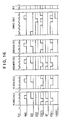
- FIG. 1 is a block diagram of an audio video interactive display;
- FIG. 2 is a block diagram illustrating the dual buffer concept;
- FIG. 3 is a block diagram of the audio video display controller which is shown generally in FIG. 1;
- FIG. 4 is a block diagram of the sync generator which is shown generally in FIG. 3;
- FIG. 5 is a block diagram of the source control logic which is shown generally in FIG. 4;
- FIG. 6 is a diagram illustrating sampling region parameters and sampling destination addresses;
- FIG. 7 is a block diagram of the FIFO shown generally in FIG. 3;
- FIG. 8 is a block diagram of the memory controller and arbiter shown generally in FIG. 3;
- FIG. 9 is a block diagram of the address generator shown generally in FIG. 3;
- FIG. 10 is a block diagram of the video buffer shown generally in FIG. 3;
- FIG. 11 is a block diagram of the serializer shown generally in FIG. 3;
- FIG. 12 is a block diagram of the color key network shown generally in FIG. 3;
- FIG. 13 is a block diagram of the digital audio circuitry shown generally in FIG. 1;
- FIG. 14 is a block diagram of the digital TV input circuitry shown generally in FIG. 1;
- FIG. 15 is a block diagram of the digital TV output circuitry shown generally in FIG. 1; and
- FIG. 16 and 17 are timing diagrams which are useful in the understanding of the invention.
- The system herein described may have many of the specific characteristics generalized to accommodate future improvements in digital television and personal computer display technologies without departing from the spirit of the invention. In this embodiment, the digital television subsystem is based on a chip set manufactured by Philips. The host system is an IBM Personal System/2 Model 70, which includes a VGA graphics (640x480x4 bit pixel) subsystem. A 12-bit luminance chrominance (Y-C) representation is referred to here, however the concepts described can be generalized to include systems with wider (e.g. 16 or more bits) data paths and higher bandwidths e.g. high definition television (HDTV). In addition, the high-resolution video described need not be limited to the bandwidth and bits/pixel provided by the VGA. Future digital TV and graphics technologies can readily be incorporated without departing from the spirit of this invention.
- FIG. 1 is a system block diagram showing how a Audio
Video Display Controller 100 interfaces to the other components of the system. It takes inputs from digitalTV input circuitry 200, ahost computer 300, and adigital audio circuitry 400. The host computer may receive input commands from input devices such as a mouse 340 andkeyboard 360. Thecontroller 100 provides outputs to thehost computer 300, a digitalTV output circuitry 500, thedigital audio circuitry 400, and a high-resolution monitor 600 via the digitalTV output circuitry 500. The digitalTV input circuitry 200 and the digitalTV output circuitry 500 are of the type set forth in Phillips Corporation's manual 9398 063 30011, date of release 6/88 entitled "Digital Video Signal Processing." - The digital
TV input circuitry 200 receives a plurality of analog input signals VIN1, VIN2 and VIN3 which may be, for example a cable TV input, a TV antenna input, a VCR input or the like. It is to be appreciated there may be more or less video inputs from different combinations of TV video sources, such as two or more VCR inputs, two or more cable inputs etc. - The digital TV input circuitry responds to these analog input signals to provide a plurality of digitized TV output signals to the audio
video display controller 100. These output signals include a TV clock or sampling clock signal TVCK; horizontal and vertical sync signals TVHS and TVVS, respectively; and a digitized TV data signal YCIN. Control signals are provided to theinput circuit 200 fromcontroller 100 on a control bus SVIN, which may also be known as an I²C bus. - The
host computer 300, which for example may be an IBM Personal System/2, the operation of which is described in detail in the IBM Personal System/2Model 50 and 60 Technical Reference, provides a plurality of signals to thecontroller 100. These signals include a PC data signal (PCDATA) which may include graphics information for insertion in the on screen portion of a TV frame buffer 145 (FIG. 3), or digitized audio to be stored in an off screen portion ofbuffer 145 for subsequent play byaudio circuit 400, or other data applications; a PC address signal (PCADDR) which indicates where PCDATA is to be stored in the frame buffer 145 (FIG. 3); PC control signals (PCCNTL); video data for high resolution display (VDAT); high resolution horizontal and vertical sync signals, (HRHS) and (HRVS), respectively; a high resolution blanking signal (HRB); a high resolution clock signal (HRCK); and high resolution red, green and blue signals, (HRRGB) from a high-resolution buffer in thehost 300 is provided to the digitalTV output circuitry 500. - The
Digital Audio Circuitry 400 receives a plurality of audio inputs such as audio in left (AINL) and audio in right (AINR) from audio sources such as microphones, CD players, stereo audio sources and the like. Audio output signals, audio out left (AOUTL) and audio out right (AOUTR) are provided to amplifiers and speakers (not shown). The control of the digital audio circuitry is provided by a plurality of signals from the audiovideo display controller 100. These signals include a sampling clock signal for audio (SCAUD); an audio control or sync signal (ACTL); and an audio data signal ADAT. - The audio
video display controller 100 responds to the respective signals frominput circuitry 200,host 300 andaudio circuitry 400 to provide a plurality of signals to the digitalTV output circuity 500. These signals include control signals on bus I²C; a TV video image out (YCOUT); and a video color switch signal (KEY) which selects between the TV image YCOUT and the high resolution image HRRGB from the host for display on thehigh resolution monitor 600. Red, green and blue output signals ROUT, GOUT and BOUT, respectively are applied to themonitor 600 fromTV output circuitry 500. - Refer now the FIG. 2 which illustrates in general the dual frame buffer concept of the invention. A more detailed description is set forth in the remaining figures. As previously stated, relative to FIG. 1, the digital
TV output circuitry 500 selects between a standard digital TV video signal from a buffer in the audiovideo display controller 100 and a high resolution graphics video signal from a buffer in thehost computer 300. In FIG. 2, alogic block 700 includes a digital TV chip set 710, which is a composite of digital TV input andoutput circuitry TV frame buffer 720 andVLSI controller 730 which are included in the audiovideo display controller 100 of FIG. 1; and aswitch 740 which is included in the digitalTV output circuitry 500 of FIG. 1. A Video Graphics Adaptor (VGA)display controller 750 and a highresolution frame buffer 760 are connected to aPC bus 770 and are included in thehost computer 300 of FIG. 1. The PC bus is also connected to the digital TV chip set 710 andcontroller 730. Thecontroller 730 receives PCDATA, PCADDR and PCCNTL on the PC bus. The PC data may be host computer graphics data which is stored in an on screen portion ofbuffer 720; or PC digital audio data which is stored in an off screen portion ofbuffer 720. This is described in detail relative to FIGS. 3 and 10. - In practice, an NTSC TV video signal is provided to chip set 710 and is converted to a digitized TV speed signal which is written to the
TV frame buffer 720 under control ofcontroller 730. A TV modified speed video signal is read from thebuffer 720, also under control ofcontroller 730 tochip set 710. The read and write operations are asynchronous with respect to each other. A TV RGB signal is then provided from chip set 710 as a first input to switch 740. This first input is from the TV Frame buffer. High resolution video information such as graphics video information is provided onPC Buss 770 toVGA display controller 750, which in turn provides high resolution pixel data to framebuffer 760.Buffer 760 provides a high resolution graphics RGB signal to a second input ofswitch 740.Switch 740 under control of control signals fromcomputer 300 selects which of thedual buffers - 1) An all TV image from
buffer 720. - 2) An all graphics image from
buffer 760. - 3) A TV image from
buffer 720 with at least one window of graphic images frombuffer 760. - 4) A graphics image from
buffer 760 with at least one window of TV images frombuffer 720. - A detailed description of the respective image generations and selection process is set forth in detail below.
- FIG. 3 is a detailed block diagram, showing the various components of the
display controller 100. Thedisplay controller 100 includestransceivers serial interface 94, async generator 105;FIFO logic 115; memory controller andarbiter 125;address generator 135;video buffer 145;serializer 155; andcolor key 165. - The general operation of audio
video display controller 100 is as follows. Async generator 105 receives the TV clock signal (TVCK), TV horizontal sync signal (TVHS) and the TV vertical sync signal (TVVS) and in response thereto generates an audio control signal (ACTL) which is sent to thedigital audio circuitry 400 and memory control andarbiter 125 to indicate when control of audio operations is to take place. A SREQ signal output is utilized by the memory control andarbiter 125 for windowing operations. - A
FIFO 115 buffers incoming TV video data YCIN under control of TVCK and SGNT from memory control andarbiter 125. Video out from theFIFO 115 is provided to the video bus (VIDBUS) when SGNT is high. The VIDBUS also receives data fromtransceiver AXCVR 90 andtransceiver XCVR 92.AXCVR 90 transmits to, and receives digital data (ADAT) fromdigital audio circuit 400.XCVR 92 receives PC data fromhost 300. This PC data may comprise graphics video in the on screen portion ofvideo buffer 145, or digital audio for storage in the off screen portion ofvideo buffer 145. Memory control andarbiter 125 controls which ofFIFO 115,AXCVR 90 andXCVR 92 is providing data to the VIDBUS at a given time, based on the state of SGNT or AGNT or PGNT, respectively. When the PC data is audio data that is stored in the off screen portion ofvideo buffer 145, this audio data may then be subsequently read out and provided to AXVR 90 and transmitted todigital audio circuit 400 for subsequent replay. - The memory controller and
arbiter 125 arbitrates for various requests for memory cycles under control of PC control signals (PCCNTL) fromhost 300. Besides the control signals utilized forFIFO 115,AXCVR 90 andXCVR 92, as discussed above, control signals are also provided to addressgenerator 135 andvideo buffer 145.Buffer 145 receives a video control signal (VBCTRL) andaddress generator 135 receives a MOP and DONE signals, which are described shortly. -
Address generator 135 receives PC addresses (PCADDR) fromhost 300 which are indicative of where PC data is to be stored. Addresses (VBAADDR) are provided to thevideo buffer 145 to indicate where data on the VIBUS is to be stored. - The PCADDR is also applied to a
serial interface 94 which connects to the I²C bus, providing SCVIN todigital input circuitry 200; SCVOUT todigital output circuitry 400, and SCAUD to digitalaudio circuitry 400. -
Serializer 155 takes the video data out fromvideo buffer 145 and provides it to digitalTV output circuitry 500.Color key 165 provides a KEY signal to digitalTV output circuitry 145 for determining which video is displayed onhigh resolution display 600 at a given time. - The main components of audio
video display controller 100 are described in detail below. - The main purpose of the
Sync Generator circuit 105, as shown in FIG. 4, is to generate requests to the memory controller for a video sampling cycle whenever the incoming TV raster is within a user-specified region. All information inside this region is written into thevideo buffer 145, while all information outside of this region is ignored. FIG. 6 illustrates how the "video sampling region" is defined. There are four parameters written to theSync Generator 105 by thehost computer 300. These are: XStart, XEnd, YStart, and YEnd. - Referring to FIG. 4, it is seen that two counters are employed to keep track of where in the TV raster the incoming video is from. For each incoming video "pixel" a horizontal counter (HCNT) 106 is incremented by the clock signal TVCK, which has the same frequency as the incoming digital video data. In this embodiment, this frequency is 13.5 MHz or 910 times the period of TVHS-. At the end of a scanline, this counter is reset (by TVHS-). In a similar manner, a vertical counter (VCNT) 107 is incremented by TVHS- one time for every scanline of incoming video. It is reset at the end of a field by the TVVS- signal. A source control logic receiver has as inputs, PCDATA, and the outputs from
counters audio timing logic 109 has a single input fromcounter 106. - The
source control logic 108 is shown in FIG. 5, and is comprised of two pairs of comparators, onepair pair XSTART 114 andXEND 115, the signal INX fromgate 116 is asserted. Similarly, when the Y- coordinate of the incoming raster falls betweenYSTART 117 andYEND 118, the signal INY fromgate 119 is asserted. When both signals are true, the raster is within the rectangular region depicted in FIG. 6, and theSync Generator 105 generates a Sample Request (SREQ) fromgate 120 to the memory controller andarbiter 135. - An additional function of the
Sync Generator 105 is to generate the appropriate timing signals to control the digital audio circuit by the audio timing logic 109 (FIG. 4). The timing is generated based on the video clock, TVCK which controls counter 106, the output of which controlslogic 109. The audio sample rate is based on an integer divisor of TVCK. For the system shown, the rate is approximately 64KHz. Every audio sample is initiated by the assertion of an Audio Request (AREQ) signal at a first output oflogic 109. An LR signal at a second output oflogic 109 toggles back and forth on every other audio request, causing the left and right audio channels to be digitized or played back on alternate audio cycles. This yields an effective sampling rate of 32 KHz per channel in this embodiment. An AUDDIR signal at a third output oflogic 109 is a control register bit that determines the type of audio cycle being requested. If AUDDIR is 0, an audio record (digitize) cycle is performed. If AUDDIR is 1, an audio playback cycle is performed. This signal is used directly to control the direction of the Audio Transceiver (AXCVR). - A Filter Clock signal (FCK) at a fourth output of
logic 109 is used to clock the pre- and post- filters at the appropriate rate. This frequency directly determines the cut-off frequency of these low-pass filters. For a sample rate of 32 KHz, the cutoff frequency should be no more than 16 KHz according to the Nyquist Theorem. If a lower sampling rate is required, for example to handle speech-quality audio, or to reduce host storage requirements, the frequency of FCK would have to be lowered correspondingly. - The
FIFO 115 shown in FIG. 7 is used to buffer the continuous stream of incoming video data while the memory controller is busy handling other requests, such as memory refresh. Whenever sampling is taking place, as indicated by SREQ being asserted atgate 116, video data online 117 is shifted into the FIFO at the rate of one video sample per TV Clock (TVCK) atgate 119. As long as the memory controller is actually performing Sample cycles (indicated by the fact that Sampling Grant online 120, or SGNT, is asserted), video data can be shifted out of the other end of the FIFO online 121, also at the TVCK rate. - If however the memory controller is busy performing another cycle, SGNT on
line 120 is not active, and no data is clocked out of the FIFO. Any samples that arrive during this time, accumulate in the FIFO. The FIFO only drives data onto the Video Bus (VIDBUS) 121 when it has been granted access to the bus (when SGNT=1) by the Memory Controller/Arbiter. - This circuit, illustrated in FIG. 8, is responsible for arbitrating between the various requests for memory cycles, and then carrying out the cycle by generating the appropriate control signals to the
video buffer 145. It also signals to the other components in the system which memory cycle it is currently performing, as well as providing an indication that the current cycle is complete. It controls access to the shared Video Data base (VIDBUS) via a request/grant protocol. Although multiple devices are attached to the Video Bus, this scheme assures that only one device at a time is allowed to drive data onto it. Finally, it can delay the host computer's I/O cycle long enough to insure that the host's data has been safely written to or read from the Video Buffer. - There are four possible requests that come to the memory controller and
arbiter 125, and are applied to thearbiter logic 126. These are: Audio Request (AREQ), Sample Request (SREQ), Transfer Request (TREQ), and PC Request (PREQ). There are two additional signals that specify the direction of the Audio and PC cycles requested. These are AUDDIR and PCDIR, respectively. In these two cases, the sequence of control signals generated depends on the whether the memory cycle is a read or a write. Each of the requests has a predefined priority in the arbitration scheme. In decreasing priority, they are: - 1. TREQ
- 2. AREQ
- 3. SREQ
- 4. PREQ
- The
arbiter 126 provides input to a memory controller section 127. When the current memory cycle is completed, a DONE signal is asserted at the output of controller 127, indicating this fact. At this time, the currently asserted request with the highest priority is serviced. If the serviced request requires use of the common Video Bus, the requesting device is given control of the bus via an appropriate Grant signal. The grant signals are Audio Grant (AGNT), PC Grant (PGNT), and Sample Grant (SGNT) provided at respective outputs ofarbiter 126. Note that the PGNT signal is used to enable the PC data bus transceiver (PXCVR), while the direction of this transceiver is controlled by the PCDIR signal. - Once arbitration is completed, the memory cycle appropriate to the winning request is performed. A memory operation code (MOP) is produced, indicating the type of memory cycle currently being performed.
- The specific sequence of control signals for the
Video Buffer 145 depends on the particular VRAM devices used to construct it. The control signals are typical of all DRAM devices, with the exception of the TR/QE- signal, which is typical of VRAMs only. Note that their are two separate Write Enable signals (WEY- and WEC-) at the output of controller 127. This allows separate write access to the Luminance (Y) and Chrominance (C) information in theVideo Buffer 145. For example, to write a monochromatic image of the incoming video, the Video Buffer could first be cleared, and then only the Luminance information would be sampled, keeping the Chrominance Write Enable signal (WEC-) inactive (high) throughout. - A typical set of timing diagrams is shown in FIGS. 16 and 17. These control sequences are generated using a generic sequences design, which progresses through multiple states until a given sequence (memory cycle) is completed. At this time the DONE signal from controller 127 is asserted, indicating to the other subsystems that the current cycle is completed.
- When the host computer requests a memory cycle (via PREQ to arbiter 126), the RDY signal from controller 127 is immediately brought inactive (low) in order to extend the host's bus cycle long enough to transfer the data to the
video buffer 145. When the data transfer is complete, the RDY signal is released, allowing thehost computer 300 to complete the bus cycle. - The
Address Generator circuit 135 shown in FIG. 9 provides all addresses for the various Video Buffer memory cycles outlined above. It includes separate, dedicated counters for Sampling 136, Host (PC) 137,Display Refresh 138, and Audio addressing 139. As various cycles repeatedly take place, this circuit automatically updates the counters so that the appropriate region of the Video Buffer is accessed. There is alarge multiplexor 140 which selects the counter output appropriate for the current operation and correctly divides the address into row and column components for successive output to the Video Buffer during RAS- and CAS- respectively. - The Sample Address Counters 136 generate a sequence of addresses that fill a rectangular region of the
Video Buffer 145 corresponding in size with the input region selected by theSync Generator 105. The upper left corner of this region is stored in two registers: Sampling Destination X-address (SDX) 141 and Sampling Destination Y-address (SDY) 142. These registers are set by the host computer using the PCDATA bus. Refer to FIG. 6. As each sampling memory cycle completes (as indicated by decoding the Memory Operation (MOP) to MOPSAMP via theMemory Operation Decoder 143, and finding DONE asserted), the Horizontal Sampling Address (HSADDR) increments across a scanline. At the end of each scanline, as signalled by TVHS-, the Vertical Sampling Address (VSADDR) is incremented by 1, and HSADDR is reset to its initial value (SDX). At the end of a field, as signalled by TVVS-, VSADDR is reset to its initial value (SDY). - The Host (PC) Address counters 137 operate in a manner very similar to the Sample Address counters 136. As each host memory cycle completes (as indicated by decoding MOP = MOPPC and DONE asserted), the Horizontal PC Address (HPADDR) increments. After a full line of video has been read from (or written to) the
video buffer 145 by thehost 300, the Vertical PC Address (VPADDR) increments, and HPADDR is reset to its initial value. The upper left corner of the region accessed by the host is determined by the PC Destination X-address (PDX)register 144 and PC Destination Y-address (PDY)register 146, both of which can be set via the host data bus (PCDATA). This auto-increment scheme allows the host computer to fill a rectangular region of theVideo Buffer 145 with a single stream-oriented instruction, such as the OUTSW or INSW instruction of the Intel 80X86 processors. - The Video Refresh Counter (VREF) 138 is used to determine which scanline of video memory is to be transferred to VRAM serial port on the next Video Refresh (TR/QE-) cycle. During each Horizontal Sync interval of the host's high resolution display (HRHS-), one scanline of VRAM must be transferred, so that the contents of the appropriate scanline in the
Video Buffer 145 can be shifted out synchronously with the high-resolution display 600. The particular sequence of Video Buffer scanlines transferred can be controlled by thehost 300 using the Refresh Mode Register (REFMODE) 147. Normally, the lines are transferred progressively, with the Video Refresh Address (VREF) incrementing by one after each scanline is transferred. This in known as progressive scan mode. This mode provides the highest effective vertical resolution, but exhibits some "scalloping" artifacts if the subject moves horizontally from one field to the next. The subject is seen in one position on the even scanlines, and in another on the odd ones in between The effect is most noticeable in distinct vertical edges with substantial horizontal motion. - For this reason, another mode, called double-scan mode, is provided. Here, each Video Refresh Address is used twice in succession, resulting in each of the incoming scanlines in the first (even) TV field being shown twice in the first high-speed output frame. During the next (odd) TV field, the Video Refresh address are again used twice each, causing the scanlines in the next-speed output frame to again be doubled. This mode has slightly lower vertical resolution than the progressive mode, but is more appropriate for images that exhibit artifacts using that mode. Since the scanlines are doubled, each high-speed output frame only contains information from one incoming TV field, so no scalloping occurs.
- The Horizontal and Vertical Audio Addresses (HAUDADDR and VAUDADDR) are produced by the auto
incrementing Audio Counters 139 when PCDATA fromhost 300 is audio data. They produce a sequence of addresses corresponding to an off-screen region portion ofVideo Buffer 145. After each audio memory cycle completes (as indicated by MOPAUD and DONE asserted), the counters increment, so that the next audio data fromhost 300 is sorted in contiguous locations in theVideo Buffer 145. - The
Address Multiplexor 140 performs two functions in parallel. First, it selects the appropriate address "type" from among the counters,Sampling 136, Host (PC) 137,Video Refresh 138, andAudio 139. Second, each of these address types must be split into it's row and column components before being driven to the VRAM array. So there are actually 8 possible inputs to theMUX 140, divided into 4 pairs. The appropriate pair is determined by examining the two high order bits of the MOP (the LSB of MOP is only used to indicate direction). The Row Address component must drive the Video Buffer Address while RAS- falls, in order to be strobed into the VRAM's Row Address latches. Once RAS- has fallen, the Column Address component of a pair is selected. Note that the Column Address component of the Video Refresh Address is always exactly 0. This is because it is necessary to start shifting video samples out of the Video Buffer starting with the leftmost sample (column 0). - The
Video Buffer 145 shown in FIG. 10 is an array of Video Memories including an on screen portion and an off screen portion. The on screen portion is used to store the live TV video image data as it comes in, and to store PC DATA when it is graphics data. In this particular embodiment, the organization is 1,024 video samples across by 512 scanlines high by 12 bits deep, being comprised of 61 Megabit (512x512x4 bit) devices. These numbers were chosen to accommodate the specific resolution and depth characteristics of the digital TV chip set used. For future digital TV systems having either higher resolution or deeper samples, it is simple to change the size of the video buffer to accommodate the new system's characteristics. The off screen portion is used to store PC DATA when it is audio data. It is to be appreciated that two separate memories could be utilized in the practice of the invention, that is a first memory to store TV video data and graphics data from thehost 300; and a second memory to store audio data from thehost 300. - The incoming data bus (VIDBUS) 148 carries all information to and from the primary port of the VRAM array. This includes incoming TV video data to be sampled, digital audio data (in PC DATA and out), and host computer graphics data (PC DATA in and out). The particular access being performed is determined via standard control signals RAS-, CAS0-, TR/QE, WEY- by the
memory controller 125 described above. The address at which a given cycle takes place is determined by VBADDR, which is provided by theAddress Generator circuit 135, also described above. As set forth above, TV video data and host computer graphics data are stored in the on screen portion; and host audio data is stored in the off screen portion ofvideo buffer 145. - Note that there are left and right halves of the Video buffer. Each half has a unique CAS-Line, which allows a 2:1 interleaved access to the Frame Buffer. This effectively halves the cycle time required to transfer data into the Buffer. This is critical, since the incoming video samples are being clocked out of the
FIFO 115 at the TVCK rate, or approximately every 70 nsec in this system. The fastest page mode cycle that can be performed using today's VRAM technology is around 90nsec. By using 2:1 interleave, effective page mode access times as fast as 45nsec are achieved, which is sufficient for current motion video data rates. For significantly higher data rates, higher interleave ratios and deeper Video Buffer organizations are required. - There are separate Write Enable signals for Luminance and Chrominance, for reasons mentioned above under the
Memory Controller 125 description. - There are two separate 12-bit serial data busses shown here, one for each of the left and right halves. Every time the VRAM serial ports are shifted via the SC signal from the
serializer 155, two separate video samples are shifted out. Theserializer 155, described below, takes these two samples and presents them sequentially. The rate at which video samples are shifted out of the VRAMs is completely independent of the rate at which video samples are put in, being limited only by the maximum serial clock frequency of the devices, which is typically 25 MHz or higher. This is the primary advantage of using VRAMSs as the video buffer, since the host's high-resolution display will in general be completely asynchronous from the incoming digital video data. Again, the effective data rate of the VRAM serial outputs is twice the serial shift clock (SC) frequency, due to the 2:1 interleaving. For output video data rates in excess of 50MHz, higher interleaving ratios or deeper buffer organizations are again required. - The
serializer 155, shown in FIG. 11, takes the incoming serial data from theVideo Buffer 145 along 2 parallel 12-bit paths, SDAT0 online 156 and SDAT1 online 157, and serializes them by amultiplexor 158, shifting them out onto the high-speed Luminance-Chrominance output data bus (YCOUT) one 12-bit sample at a time by flip-flop 159. The YCOUT is clocked synchronously with the host's high resolution display dot clock (HRCK). In the present embodiment, it is clocked using the same signal. This clock frequency can be increased by some fractional amount while remaining synchronous with HRCK using conventional phase-locked loop techniques. This may be necessary, for example, to correct the aspect ratio of the video image on the high-resolution screen. There is also a high-resolution blanking signal (HRB-), which is used to force the YCOUT data to 0 (black) and also to delay the start of clocking data out of the Video Buffer's serial ports (via SC) fromgate 160 as controlled by flip-flop 161, until the active portion of the high-resolution scanline starts. - The
Color Key circuit 165, shown in FIG. 12, is used to generate a keying signal (KEY) onoutput line 166, which in turn is used by the digitalTV output circuitry 500 to switch between TV video pixels (from the YCOUT bus) and the pixels from the host's high-resolution graphics controller. With reference to FIG. 2, every pixel during which KEY is asserted is seen on the monitor as video from theTV frame buffer 720, while those during which KEY is low are seen as video from the high-resolution frame buffer 760. - The KEY signal on
line 166 from keyselect logic 167 is determined incomparator 168 by comparing the incoming high-resolution pixel with two pre-defined colors set by the host computer as manifested byKey 1logic 169 andKey 2logic 170. If the incoming pixel is between the two programmed values (R1 < A < R2), the key signal is asserted. This allows a range of colors to be specified for which video will be overlayed. If it is desired to have only one specific color overlayed with video, the KEY signal should be derived from the A=R1 comparator 168 output and R1 should be programmed with the keying color. - Several interesting effects can be obtained by using different outputs of the
comparator 168. For example, if the A < R1 output is used, all high-resolution pixels having a value less than R1 are seen as video. By painting a graphics object with concentric rings of increasing color value, interesting "growing" and shrinking" window effects can be achieved by dynamically varying the threshold value, R1. - This circuitry, shown in FIG. 13, serves as the audio Input/Output subsystem in the system. The incoming analog stereo audio (
AINL 402 and AINR 404) signals to input gain andbalance control circuit 406 are first gain and balance adjusted appropriately and are subsequently low-pass prefiltered, so that they contain no frequency content above the Nyquist Frequency. The gain and balance can be controlled by thehost computer 300 via the 2-bit serial data bus 408 (SCAUD). - Once the signals have been conditioned, they must be multiplexed onto a common wire by a
multiplexor 410, in order to avoid the need for two separate Analog-to-Digital (A/D) convertors. Every other audio sample written into the video buffer comes from alternating channels of the incoming audio source. This toggling is performed via the L/R signal 412 generated by thesync generator 105. Thesync generator 105 also generates the basic timing pulses for the audio conversion processes. When the digital audio data is being recorded, (AUDDIR=0) online 414, the timing pulses (AREQ) online 416 are applied only to the A/D convertor 418 viagate 420. Similarly, if AUDDIR=1 (playback mode) online 414, AREQ online 416 are only be applied to the Digital-to-Analog convertor (DAC) 422 viagate 424. Each time one of theconvertors - The DAC used in this system is actually a dual channel DAC, taking a single digital input and providing two analog outputs. The two output voltages are updated on every other DAC conversion cycle, in a similar manner to the A/D. After the DAC, there is once again analog audio, which must be processed through a
reconstruction filter 426 in order to remove unwanted artifacts of the sampling process (i.e. quantization noise). This reconstruction filter has a cutoff frequency identical to that of the input filter. The cutoff frequency is controlled by the frequency of the FCK signal from theSync Generator 105. Thus, a range of sample rates (hence cutoff frequencies) can be accommodated. Finally, there is anoutput amplifier 428, to restore the signals to a level sufficient to drive an audio pre-amp or headphones. - An interesting additional feature of this circuit is the ability to monitor the digital audio through the DAC as it is being recorded from the A/D. This can be done by driving both the A/D and DAC convert pulses simultaneously, which requires an obvious change in the logic shown in FIG. 13. This feature is a result of the fact that the A/D and DAC share a common data bus (ADAT).
- FIG. 14 shows a typical system for providing the digital video input processed by the rest of the system. The video input can be selected by a video source
select logic 202 from one of several sources under host control through the use of a I²C serial control bus. (This bus is standard for control Philips chips and described in Signetics/Philips data books as previously referenced). In addition, these sources can be any of a variety of formats including PAL, NTSC, SECAM, SVHS,RGB, etc. This is a virtue of the digital television approach, since these devices have been designed with that flexibility in mind. After a source is selected, it is digitized using a conventional video A/D convertor 204. An 8 bit digital output is shown, but again, this is not a fundamental limitation, and higher resolutions provided by future systems can be readily accommodated. This digitized video is then processed by a Digital Multi-Standard Decoder (DMSD) 206, driving a 12-bit digital Luminance/Chrominance Input Bus (YCIN) 208 at the TV data rate (TVCK). It is theDMSD 206 that interprets the variety of input video formats and decodes them appropriately. Various parameters of the decoder can be adjusted via the serial control bus I²C. - A
Sync Separator circuit 210 simply extracts Sync and Clock information from the currently selected video input and provides this information (TVVS-, TVHS-,TVCK) to the rest of the system. - This circuit, shown in FIG. 15, converts the high-speed Luminance/Chrominance Bus (YCOUT) information on
line 502 back to analog RGB form by aconvertor 504 and video Y and C toRGB matrix 506, and multiplexes it in amultiplexer 508 withRGB signals 510 from the host's high-resolution graphics controller, under control of the KEY signals online 511. - The Y/C to
RGB Matrix 506 is a purely analog component which converts the analog Y/C representation to RGB using a standard conversion matrix. Various adjustments to the output video (Saturation, Contrast, and Brightness) can be made by the host via the serial control bus I²C. - Finally, the
Video Multiplexor 508 selects between the RGB-converted video and the RGB from the high-resolution display controller, on a pixel by pixel basis. This selection is done under control of the KEY signal online 511 generated by the Color Key circuit of FIG. 12. Theoutput 512 of themultiplexor 508 directly drives the high-resolution display 600.
Claims (19)
a high resolution monitor (600);
a computer (300) for providing control signals, including a high resolution frame buffer (760) for storing computer graphics images pel by pel, and reading out said graphics images on a pel by pel basis at a rate controlled by said control signals;
a TV video controller (100), including a TV frame buffer which stores TV video at TV speeds and reads out TV video on a pel by pel basis at a rate controlled by said control signals from said computer; and
a switching mechanism (500) controlled by said control signals from said computer for selectively switching between said high resolution frame buffer and said TV frame buffer on a pel by pel basis to read out said buffers to display the read out video on said high resolution monitor.
a high resolution display (600);
a computer system (300) for generating control signals, and including a high resolution frame buffer (760) for storing video graphics pel by pel for display on said high resolution display, including means for converting the video graphics to an analog high resolution graphics signal;
an input device (200) for receiving standard analog TV signals and converting them to standard digital TV signals;
a display controller (100) which operates under control of said control signals from said computer, said display controller including a two port TV frame buffer, with said standard digital TV signal being read into the first port at a TV rate, for storage, and being read out of the second port on a pel by pel basis at a higher speed rate controlled by said control signals from said computer; and
an output device (500) including a digital to analog converter (504) for converting the standard digital TV signal read out of the second port to an analog TV signal, and further including means (508) for selecting a pel at a time one of said analog high resolution graphics signal and said analog TV signal for display on said high resolution display.
a sync generator (105) responsive to a TV clock signal, horizontal sync signal and vertical signal portion of said standard digital TV signal to provide a TV sync signal for reading the data portion of said standard TV signal into said first port of said TV frame buffer; and
a serializer (155) operating under control of said control signals from said computer for reading out the digital TV data from said second port of said TV frame buffer on a pel by pel basis to provide serial TV data at a high resolution rate; and
a select network (508) responsive to said control signals from said computer for providing a key signal which when in a first state selects said TV video for display and when in a second state selects said high resolution graphics video for display.
a high resolution display (600);
a computer system (300) for generating control signals, and video graphics signals;
an input device (200) for receiving standard analog TV signals and converting them to standard digital TV signals;
a display controller (100) which operates under control of said control signals from said computer, said display controller including a two port display frame buffer, with one of said standard digital TV signal and said video graphics signal being read into the first port at a first rate, and being read out of the second port pel by pel at a second rate controlled by said control signals from said computer; and
an output device (500) including a digital to analog converter for converting the signal read out of the second port of said display frame buffer to an analog display signal, for display on said high resolution display.
a high resolution display;
a computer system for generating control signals, video graphics signals, and digitized audio signals;
an input device for receiving standard analog TV signals and converting them to standard digital TV signals;
a display controller which operates under control of said control signals from said computer, said display controller including a display frame buffer which includes an on screen portion and an off screen portion, with said standard digital TV signal and said video graphics signal being read for storage in predetermined locations in said on screen portion of said display frame buffer, with said digitized audio signals being read for storage in said off screen portion of said display frame buffer, and each being read out in response to said control signals from said computer;
an audio circuit responsive to the digitized audio signals read out of said display frame buffer, including means for converting the digitized audio to analog audio; and
an output device including a digital to analog converter for converting the standard TV signal and the video graphics signals read out of said TV frame buffer to an analog TV signal, for display on said high resolution display.
a high resolution frame buffer (760) for storing video graphics, including means for reading out said video graphics at a rate controlled by said control signals; and
means for converting the video graphics to an analog high resolution graphics signal; and
wherein said output device includes:
means for selecting one of said analog high resolution graphics signal and said analog display signal for display on said high resolution display.
a high resolution display;
a computer system for generating computer control signals, and computer data signals which include graphics data signals, and digitized audio data signals;
an input device for receiving standard analog TV signals and converting them to standard digital TV signals;
a display controller which operates under control of said computer control signals from said computer, said display controller including a two port data buffer which includes an on screen portion and an off screen portion, with said standard digital TV signal and said computer data signals being read into the first port for storage of the digital TV signal and the graphics data signals in predetermined locations in said on screen portion of said data buffer, and for storage of said digitized audio data signals in said off screen portion of said data buffer, with said digitized audio data signals being read out of said first port under control of said computer control signals and said digital TV signal and the graphics data signals being read out of the second port at a speed controlled by said computer control signals;
an audio circuit responsive to the digitized audio data signals read out of the first port of said display frame buffer, including means for converting the digitized audio data signals to analog audio; and
an output device including a digital to analog converter for converting the standard TV signal and the graphics data signals read out of the second port of said data buffer to an analog display signal, for display on said high resolution display.
a sync generator responsive to said standard digital TV signal to provide a TV sync signal for reading the data portion of said standard TV signal into said first port of said data buffer; and
a serializer operating under control of said computer control signals for reading out display data from said second port of said data buffer to provide display data at a high resolution rate to said output device.
a high resolution frame buffer for storing video graphics, including means for reading out said video graphics at a rate controlled by said computer system;
means for converting the video graphics to an analog high resolution graphics signal;
wherein said output device includes:
means for selecting one of said analog high resolution graphics signal and said analog display signal for display on said high resolution display.
a high resolution display;
a computer system for generating control signals, video graphics signals, and first digitized audio signals;
an input device for receiving standard analog TV signals and converting them to standard digital TV signals;
a display controller which operates under control of said control signals from said computer, said display controller including a display frame buffer which includes an on screen portion and an off screen portion, with said standard digital TV signal and said video graphics signal being read for storage in predetermined locations in said on screen portion of said display frame buffer, with said first digitized audio signals being read for storage in said off screen portion of said display frame buffer, and each being read out in response to said control signals from said computer;
a source of analog audio signals;
an audio circuit including means for converting said analog audio signals to second digitized audio signals to be read into the off screen portion of said TV frame buffer for storage at predetermined locations, and being read out under control of said control signals and being responsive to either the first digitized audio signals or the second digitized audio signals read out of said display frame buffer, including means for converting the digitized audio to analog audio; and
an output device including a digital to analog converter for converting the standard TV signal and the video graphics read out of said TV frame buffer to an analog TV signal, for display on said high resolution display.
a high resolution frame buffer for storing video graphics, including means for reading out said video graphics at a rate controlled by said control signals; and
means for converting the video graphics to an analog high resolution graphics signal; and
wherein said output device includes:
means for selecting one of said analog high resolution graphics signal and said analog display signal for display on said high resolution display.
a high resolution display;
a computer system for generating computer control signals, and computer data signals which include graphics data signals, and first digitized audio data signals;
an input device for receiving standard analog TV signals and converting them to standard digital TV signals;
a display controller which operates under control of said computer control signals from said computer, said display controller including a two port data buffer which includes an on screen portion and an off screen portion, with said standard digital TV signal and said computer data signals being read into the first port for storage of the digital TV signal and the graphics data signals in predetermined locations in said on screen portion of said data buffer, and for storage of said first digitized audio data signals in said off screen portion of said data buffer, with said first digitized audio data signals being read out of said first port under control of said computer control signals and said digital TV signal and the graphics data signal being read out of the second port at a speed controlled by said computer control signals;
a source of analog audio signals;
an audio circuit including means for converting said analog audio signals to second digitized audio signals to be read into the first port of said data buffer for storage at predetermined locations of said off screen portion, and being read out of said first port under control of said control signals and being responsive to either the first digitized audio data signals or the second digitized audio signals read out of the first port of said display frame buffer, including means for converting the digitized audio signals read out of said first port to analog audio; and
an output device including a digital to analog converter for converting the standard TV signal and the graphics data signals read out of the second port of said data buffer to an analog display signal, for display on said high resolution display.
Applications Claiming Priority (2)
| Application Number | Priority Date | Filing Date | Title |
|---|---|---|---|
| US314623 | 1989-02-23 | ||
| US07/314,623 US4994912A (en) | 1989-02-23 | 1989-02-23 | Audio video interactive display |
Publications (3)
| Publication Number | Publication Date |
|---|---|
| EP0384257A2 true EP0384257A2 (en) | 1990-08-29 |
| EP0384257A3 EP0384257A3 (en) | 1992-06-03 |
| EP0384257B1 EP0384257B1 (en) | 1995-10-04 |
Family
ID=23220711
Family Applications (1)
| Application Number | Title | Priority Date | Filing Date |
|---|---|---|---|
| EP90102671A Expired - Lifetime EP0384257B1 (en) | 1989-02-23 | 1990-02-12 | Audio video interactive display |
Country Status (5)
| Country | Link |
|---|---|
| US (1) | US4994912A (en) |
| EP (1) | EP0384257B1 (en) |
| JP (1) | JPH0820857B2 (en) |
| CA (1) | CA2000021C (en) |
| DE (1) | DE69022752T2 (en) |
Cited By (30)
| Publication number | Priority date | Publication date | Assignee | Title |
|---|---|---|---|---|
| EP0419814A2 (en) * | 1989-09-29 | 1991-04-03 | International Business Machines Corporation | Pixel protection mechanism for mixed graphics/video display adaptors |
| EP0484981A2 (en) * | 1990-11-09 | 1992-05-13 | Fuji Photo Film Co., Ltd. | Image data processing apparatus |
| EP0488125A2 (en) * | 1990-11-29 | 1992-06-03 | ESG Elektronik-System-Gesellschaft mbH | Multi-function display unit |
| WO1993021623A1 (en) * | 1992-04-17 | 1993-10-28 | Intel Corporation | Visual frame buffer architecture |
| EP0574747A2 (en) * | 1992-06-19 | 1993-12-22 | Intel Corporation | Visual frame buffer architecture |
| EP0574748A2 (en) * | 1992-06-19 | 1993-12-22 | Intel Corporation | Scalable multimedia platform architecture |
| EP0601647A1 (en) * | 1992-12-11 | 1994-06-15 | Koninklijke Philips Electronics N.V. | System for combining multiple-format multiple-source video signals |
| EP0610829A1 (en) * | 1993-02-05 | 1994-08-17 | Brooktree Corporation | System for, and method of, displaying information from a graphics memory and a video memory on a display monitor |
| US5426731A (en) * | 1990-11-09 | 1995-06-20 | Fuji Photo Film Co., Ltd. | Apparatus for processing signals representative of a computer graphics image and a real image |
| EP0682334A1 (en) * | 1994-05-10 | 1995-11-15 | ESSILOR INTERNATIONAL Compagnie Générale d'Optique | Process for transforming a video image into an image for a matrix display |
| WO1996015499A1 (en) * | 1994-11-10 | 1996-05-23 | Brooktree Corporation | System and method for command processing and data transfer in a computer system for sound or the like |
| EP0741379A1 (en) * | 1995-05-04 | 1996-11-06 | Winbond Electronics Corporation | Scaled video output overlaid onto a computer graphics output |
| CN1034150C (en) * | 1992-12-11 | 1997-02-26 | 菲利浦光灯制造公司 | System for combining multiple-format multiple-source video signals |
| US5719511A (en) * | 1996-01-31 | 1998-02-17 | Sigma Designs, Inc. | Circuit for generating an output signal synchronized to an input signal |
| EP0782333A3 (en) * | 1995-12-25 | 1998-07-29 | Hitachi, Ltd. | Image display apparatus |
| US5790881A (en) * | 1995-02-07 | 1998-08-04 | Sigma Designs, Inc. | Computer system including coprocessor devices simulating memory interfaces |
| US5797029A (en) * | 1994-03-30 | 1998-08-18 | Sigma Designs, Inc. | Sound board emulation using digital signal processor using data word to determine which operation to perform and writing the result into read communication area |
| US5818468A (en) * | 1996-06-04 | 1998-10-06 | Sigma Designs, Inc. | Decoding video signals at high speed using a memory buffer |
| US5821947A (en) * | 1992-11-10 | 1998-10-13 | Sigma Designs, Inc. | Mixing of computer graphics and animation sequences |
| US5890190A (en) * | 1992-12-31 | 1999-03-30 | Intel Corporation | Frame buffer for storing graphics and video data |
| EP0954171A1 (en) * | 1998-04-29 | 1999-11-03 | CANAL+ Société Anonyme | Receiver/decoder and method of processing video data |
| US6084909A (en) * | 1994-03-30 | 2000-07-04 | Sigma Designs, Inc. | Method of encoding a stream of motion picture data |
| US6124897A (en) * | 1996-09-30 | 2000-09-26 | Sigma Designs, Inc. | Method and apparatus for automatic calibration of analog video chromakey mixer |
| US6128726A (en) * | 1996-06-04 | 2000-10-03 | Sigma Designs, Inc. | Accurate high speed digital signal processor |
| EP1136906A2 (en) * | 1990-11-30 | 2001-09-26 | Sun Microsystems, Inc. | Improved method and apparatus for creating virtual worlds |
| US6421096B1 (en) | 1994-06-28 | 2002-07-16 | Sigman Designs, Inc. | Analog video chromakey mixer |
| EP1227675A2 (en) * | 2001-01-19 | 2002-07-31 | SAMSUNG ELECTRONICS Co. Ltd. | Device and method for realizing tranparency in an on screen display |
| WO2003019512A2 (en) * | 2001-08-22 | 2003-03-06 | Gary Alfred Demos | Method and apparatus for providing computer-compatible fully synchronized audio/video information |
| EP1629667A2 (en) * | 2003-05-30 | 2006-03-01 | Karl Storz GmbH & Co. KG | Method and device for displaying medical patient data on a medical display unit |
| US7703003B2 (en) | 2001-10-01 | 2010-04-20 | Oracle America, Inc. | XML document frameworks |
Families Citing this family (103)
| Publication number | Priority date | Publication date | Assignee | Title |
|---|---|---|---|---|
| US4855725A (en) | 1987-11-24 | 1989-08-08 | Fernandez Emilio A | Microprocessor based simulated book |
| US5327243A (en) * | 1989-12-05 | 1994-07-05 | Rasterops Corporation | Real time video converter |
| US5229852A (en) * | 1989-12-05 | 1993-07-20 | Rasterops Corporation | Real time video converter providing special effects |
| US5594467A (en) * | 1989-12-06 | 1997-01-14 | Video Logic Ltd. | Computer based display system allowing mixing and windowing of graphics and video |
| JPH05324821A (en) * | 1990-04-24 | 1993-12-10 | Sony Corp | High-resolution video and graphic display device |
| US5257348A (en) * | 1990-05-24 | 1993-10-26 | Apple Computer, Inc. | Apparatus for storing data both video and graphics signals in a single frame buffer |
| US5680151A (en) * | 1990-06-12 | 1997-10-21 | Radius Inc. | Method and apparatus for transmitting video, data over a computer bus using block transfers |
| US5229760A (en) * | 1990-06-28 | 1993-07-20 | Xerox Corporation | Arithmetic technique for variable resolution printing in a ros |
| US5228859A (en) * | 1990-09-17 | 1993-07-20 | Interactive Training Technologies | Interactive educational and training system with concurrent digitized sound and video output |
| US5327156A (en) * | 1990-11-09 | 1994-07-05 | Fuji Photo Film Co., Ltd. | Apparatus for processing signals representative of a computer graphics image and a real image including storing processed signals back into internal memory |
| US5138459A (en) | 1990-11-20 | 1992-08-11 | Personal Computer Cameras, Inc. | Electronic still video camera with direct personal computer (pc) compatible digital format output |
| JP2896414B2 (en) * | 1991-02-08 | 1999-05-31 | 鹿島建設株式会社 | Display device |
| CA2065979C (en) * | 1991-06-10 | 1999-01-19 | Stephen Patrick Thompson | Mode dependent minimum fifo fill level controls processor access to video memory |
| US5420856A (en) * | 1991-06-18 | 1995-05-30 | Multimedia Design, Inc. | High-speed multi-media switching system |
| US6088045A (en) * | 1991-07-22 | 2000-07-11 | International Business Machines Corporation | High definition multimedia display |
| US5351067A (en) * | 1991-07-22 | 1994-09-27 | International Business Machines Corporation | Multi-source image real time mixing and anti-aliasing |
| GB9120032D0 (en) * | 1991-09-19 | 1991-11-06 | Saulsbury Ashley | An interactive communication device |
| US5157495A (en) * | 1991-12-20 | 1992-10-20 | Eastman Kodak Company | Multi-mode video standard selection circuit and selection method |
| US5642437A (en) * | 1992-02-22 | 1997-06-24 | Texas Instruments Incorporated | System decoder circuit with temporary bit storage and method of operation |
| IT1259343B (en) * | 1992-03-17 | 1996-03-12 | Sip | VIDEO CONTROL CIRCUIT FOR MULTIMEDIA APPLICATIONS |
| JP3280116B2 (en) * | 1992-04-29 | 2002-04-30 | キヤノン株式会社 | Real-time interactive image processing device |
| KR950008714B1 (en) * | 1992-05-12 | 1995-08-04 | 삼성전자주식회사 | Osd apparatus & method in multi-mode monitor |
| US5404448A (en) * | 1992-08-12 | 1995-04-04 | International Business Machines Corporation | Multi-pixel access memory system |
| US20020091850A1 (en) * | 1992-10-23 | 2002-07-11 | Cybex Corporation | System and method for remote monitoring and operation of personal computers |
| KR950014157B1 (en) * | 1992-10-29 | 1995-11-22 | 대우전자주식회사 | Scanning method converted for image-data |
| US5402147A (en) * | 1992-10-30 | 1995-03-28 | International Business Machines Corporation | Integrated single frame buffer memory for storing graphics and video data |
| US5420801A (en) * | 1992-11-13 | 1995-05-30 | International Business Machines Corporation | System and method for synchronization of multimedia streams |
| US5729556A (en) * | 1993-02-22 | 1998-03-17 | Texas Instruments | System decoder circuit with temporary bit storage and method of operation |
| US5657423A (en) * | 1993-02-22 | 1997-08-12 | Texas Instruments Incorporated | Hardware filter circuit and address circuitry for MPEG encoded data |
| US5412426A (en) * | 1993-04-16 | 1995-05-02 | Harris Corporation | Multiplexing of digitally encoded NTSC and HDTV signals over single microwave communication link from television studio to tower transmitter facility for simultaneous broadcast (simulcast) to customer sites by transmitter facility |
| US5502727A (en) * | 1993-04-20 | 1996-03-26 | At&T Corp. | Image and audio communication system having graphical annotation capability |
| CA2100700C (en) * | 1993-07-16 | 2000-01-11 | Robert P. Bicevskis | Multi-media computer architecture |
| US5617367A (en) * | 1993-09-01 | 1997-04-01 | Micron Technology, Inc. | Controlling synchronous serial access to a multiport memory |
| USRE38610E1 (en) * | 1993-09-30 | 2004-10-05 | Ati Technologies, Inc. | Host CPU independent video processing unit |
| US5523791A (en) * | 1993-10-12 | 1996-06-04 | Berman; John L. | Method and apparatus for applying overlay images |
| US5583652A (en) * | 1994-04-28 | 1996-12-10 | International Business Machines Corporation | Synchronized, variable-speed playback of digitally recorded audio and video |
| US5765142A (en) * | 1994-08-18 | 1998-06-09 | Creatacard | Method and apparatus for the development and implementation of an interactive customer service system that is dynamically responsive to change in marketing decisions and environments |
| US5764964A (en) * | 1994-10-13 | 1998-06-09 | International Business Machines Corporation | Device for protecting selected information in multi-media workstations |
| US6037926A (en) * | 1994-11-18 | 2000-03-14 | Thomson Consumer Electronics, Inc. | Emulation of computer monitor in a wide screen television |
| US6014125A (en) * | 1994-12-08 | 2000-01-11 | Hyundai Electronics America | Image processing apparatus including horizontal and vertical scaling for a computer display |
| US5598525A (en) | 1995-01-23 | 1997-01-28 | Cirrus Logic, Inc. | Apparatus, systems and methods for controlling graphics and video data in multimedia data processing and display systems |
| US5896179A (en) * | 1995-03-31 | 1999-04-20 | Cirrus Logic, Inc. | System for displaying computer generated images on a television set |
| JPH08331472A (en) * | 1995-05-24 | 1996-12-13 | Internatl Business Mach Corp <Ibm> | Method and apparatus for synchronizing video data with graphic data in multimedia display device containing communal frame buffer |
| US6359636B1 (en) | 1995-07-17 | 2002-03-19 | Gateway, Inc. | Graphical user interface for control of a home entertainment system |
| US5675390A (en) * | 1995-07-17 | 1997-10-07 | Gateway 2000, Inc. | Home entertainment system combining complex processor capability with a high quality display |
| US5812144A (en) * | 1995-09-08 | 1998-09-22 | International Business Machines Corporation | System for performing real-time video resizing in a data processing system having multimedia capability |
| US5940610A (en) * | 1995-10-05 | 1999-08-17 | Brooktree Corporation | Using prioritized interrupt callback routines to process different types of multimedia information |
| US5892982A (en) * | 1995-11-29 | 1999-04-06 | Matsushita Electric Industrial Co., Ltd. | External expansion bus interface circuit for connecting a micro control unit, and a digital recording and reproducing apparatus incorporating said interface circuit |
| US5663748A (en) * | 1995-12-14 | 1997-09-02 | Motorola, Inc. | Electronic book having highlighting feature |
| US5815407A (en) * | 1995-12-14 | 1998-09-29 | Motorola Inc. | Method and device for inhibiting the operation of an electronic device during take-off and landing of an aircraft |
| US5697793A (en) * | 1995-12-14 | 1997-12-16 | Motorola, Inc. | Electronic book and method of displaying at least one reading metric therefor |
| US5661635A (en) * | 1995-12-14 | 1997-08-26 | Motorola, Inc. | Reusable housing and memory card therefor |
| US5893132A (en) * | 1995-12-14 | 1999-04-06 | Motorola, Inc. | Method and system for encoding a book for reading using an electronic book |
| US5761681A (en) * | 1995-12-14 | 1998-06-02 | Motorola, Inc. | Method of substituting names in an electronic book |
| US5761682A (en) * | 1995-12-14 | 1998-06-02 | Motorola, Inc. | Electronic book and method of capturing and storing a quote therein |
| US5657088A (en) * | 1995-12-22 | 1997-08-12 | Cirrus Logic, Inc. | System and method for extracting caption teletext information from a video signal |
| US6292176B1 (en) * | 1996-02-26 | 2001-09-18 | Motorola, Inc. | Method and system for displaying textual information |
| US5914711A (en) * | 1996-04-29 | 1999-06-22 | Gateway 2000, Inc. | Method and apparatus for buffering full-motion video for display on a video monitor |
| JPH1079915A (en) * | 1996-09-02 | 1998-03-24 | Mitsubishi Electric Corp | Recording and reproducing device |
| US6195086B1 (en) * | 1996-09-12 | 2001-02-27 | Hearme | Method and apparatus for loosely synchronizing closed free running raster displays |
| KR100233388B1 (en) * | 1996-10-11 | 1999-12-01 | 구자홍 | Pctv display apparatus |
| US6437829B1 (en) * | 1997-01-16 | 2002-08-20 | Display Laboratories, Inc. | Alignment of cathode ray tube displays using a video graphics controller |
| US6546426B1 (en) | 1997-03-21 | 2003-04-08 | International Business Machines Corporation | Method and apparatus for efficiently processing an audio and video data stream |
| JP3564961B2 (en) | 1997-08-21 | 2004-09-15 | 株式会社日立製作所 | Digital broadcast receiver |
| AU774003B2 (en) * | 1998-09-22 | 2004-06-10 | Avocent Huntsville Corporation | System for accessing personal computers remotely |
| US7046308B1 (en) * | 1998-11-13 | 2006-05-16 | Hewlett-Packard Development Company, L.P. | Method and apparatus for transmitting digital television data |
| US6694379B1 (en) * | 1999-04-09 | 2004-02-17 | Sun Microsystems, Inc. | Method and apparatus for providing distributed clip-list management |
| US6573946B1 (en) * | 2000-08-31 | 2003-06-03 | Intel Corporation | Synchronizing video streams with different pixel clock rates |
| US20030014674A1 (en) * | 2001-07-10 | 2003-01-16 | Huffman James R. | Method and electronic book for marking a page in a book |
| US7313764B1 (en) * | 2003-03-06 | 2007-12-25 | Apple Inc. | Method and apparatus to accelerate scrolling for buffered windows |
| CN1327695C (en) * | 2004-10-18 | 2007-07-18 | 海信集团有限公司 | TV circuit realizing high resolution 1080P/60 format |
| US20060168537A1 (en) * | 2004-12-22 | 2006-07-27 | Hochmuth Roland M | Computer display control system and method |
| US8631342B2 (en) * | 2004-12-22 | 2014-01-14 | Hewlett-Packard Development Company, L.P. | Computer display control system and method |
| CN101496387B (en) * | 2006-03-06 | 2012-09-05 | 思科技术公司 | System and method for access authentication in a mobile wireless network |
| EP2048666A1 (en) * | 2007-10-12 | 2009-04-15 | Magix Ag | System and Method of automatically creating a multi/hybrid multimedia storage medium |
| US8797377B2 (en) * | 2008-02-14 | 2014-08-05 | Cisco Technology, Inc. | Method and system for videoconference configuration |
| US10229389B2 (en) * | 2008-02-25 | 2019-03-12 | International Business Machines Corporation | System and method for managing community assets |
| US8694658B2 (en) * | 2008-09-19 | 2014-04-08 | Cisco Technology, Inc. | System and method for enabling communication sessions in a network environment |
| US8659637B2 (en) * | 2009-03-09 | 2014-02-25 | Cisco Technology, Inc. | System and method for providing three dimensional video conferencing in a network environment |
| US20100283829A1 (en) * | 2009-05-11 | 2010-11-11 | Cisco Technology, Inc. | System and method for translating communications between participants in a conferencing environment |
| US8659639B2 (en) | 2009-05-29 | 2014-02-25 | Cisco Technology, Inc. | System and method for extending communications between participants in a conferencing environment |
| US9082297B2 (en) * | 2009-08-11 | 2015-07-14 | Cisco Technology, Inc. | System and method for verifying parameters in an audiovisual environment |
| US9225916B2 (en) * | 2010-03-18 | 2015-12-29 | Cisco Technology, Inc. | System and method for enhancing video images in a conferencing environment |
| US9313452B2 (en) | 2010-05-17 | 2016-04-12 | Cisco Technology, Inc. | System and method for providing retracting optics in a video conferencing environment |
| US8896655B2 (en) | 2010-08-31 | 2014-11-25 | Cisco Technology, Inc. | System and method for providing depth adaptive video conferencing |
| US8599934B2 (en) | 2010-09-08 | 2013-12-03 | Cisco Technology, Inc. | System and method for skip coding during video conferencing in a network environment |
| US8599865B2 (en) | 2010-10-26 | 2013-12-03 | Cisco Technology, Inc. | System and method for provisioning flows in a mobile network environment |
| US8699457B2 (en) | 2010-11-03 | 2014-04-15 | Cisco Technology, Inc. | System and method for managing flows in a mobile network environment |
| US8730297B2 (en) | 2010-11-15 | 2014-05-20 | Cisco Technology, Inc. | System and method for providing camera functions in a video environment |
| US9143725B2 (en) | 2010-11-15 | 2015-09-22 | Cisco Technology, Inc. | System and method for providing enhanced graphics in a video environment |
| US8902244B2 (en) | 2010-11-15 | 2014-12-02 | Cisco Technology, Inc. | System and method for providing enhanced graphics in a video environment |
| US9338394B2 (en) | 2010-11-15 | 2016-05-10 | Cisco Technology, Inc. | System and method for providing enhanced audio in a video environment |
| US8542264B2 (en) | 2010-11-18 | 2013-09-24 | Cisco Technology, Inc. | System and method for managing optics in a video environment |
| US8723914B2 (en) | 2010-11-19 | 2014-05-13 | Cisco Technology, Inc. | System and method for providing enhanced video processing in a network environment |
| US9111138B2 (en) | 2010-11-30 | 2015-08-18 | Cisco Technology, Inc. | System and method for gesture interface control |
| US8692862B2 (en) | 2011-02-28 | 2014-04-08 | Cisco Technology, Inc. | System and method for selection of video data in a video conference environment |
| US8670019B2 (en) | 2011-04-28 | 2014-03-11 | Cisco Technology, Inc. | System and method for providing enhanced eye gaze in a video conferencing environment |
| US8786631B1 (en) * | 2011-04-30 | 2014-07-22 | Cisco Technology, Inc. | System and method for transferring transparency information in a video environment |
| US8934026B2 (en) | 2011-05-12 | 2015-01-13 | Cisco Technology, Inc. | System and method for video coding in a dynamic environment |
| US8947493B2 (en) | 2011-11-16 | 2015-02-03 | Cisco Technology, Inc. | System and method for alerting a participant in a video conference |
| US8682087B2 (en) | 2011-12-19 | 2014-03-25 | Cisco Technology, Inc. | System and method for depth-guided image filtering in a video conference environment |
| US9681154B2 (en) | 2012-12-06 | 2017-06-13 | Patent Capital Group | System and method for depth-guided filtering in a video conference environment |
| US9843621B2 (en) | 2013-05-17 | 2017-12-12 | Cisco Technology, Inc. | Calendaring activities based on communication processing |
Citations (4)
| Publication number | Priority date | Publication date | Assignee | Title |
|---|---|---|---|---|
| JPS5881386A (en) * | 1981-11-10 | 1983-05-16 | Sony Corp | Television receiver |
| US4599611A (en) * | 1982-06-02 | 1986-07-08 | Digital Equipment Corporation | Interactive computer-based information display system |
| WO1988009540A1 (en) * | 1987-05-18 | 1988-12-01 | Denyse Dubrucq | The information station |
| EP0300509A2 (en) * | 1987-07-24 | 1989-01-25 | Matsushita Electric Industrial Co., Ltd. | Display apparatus capable of simultaneously displaying a television picture and a compressed display page of character and graphics data |
Family Cites Families (27)
| Publication number | Priority date | Publication date | Assignee | Title |
|---|---|---|---|---|
| US4357624A (en) * | 1979-05-15 | 1982-11-02 | Combined Logic Company | Interactive video production system |
| US4282546A (en) * | 1979-11-28 | 1981-08-04 | Rca Corporation | Television image size altering apparatus |
| US4317114A (en) * | 1980-05-12 | 1982-02-23 | Cromemco Inc. | Composite display device for combining image data and method |
| USRE32201F1 (en) * | 1981-08-12 | 1989-08-01 | Ibm | Apparatus and method for reading and writing text characters in a graphics display |
| US4710873A (en) * | 1982-07-06 | 1987-12-01 | Marvin Glass & Associates | Video game incorporating digitized images of being into game graphics |
| US4562435A (en) * | 1982-09-29 | 1985-12-31 | Texas Instruments Incorporated | Video display system using serial/parallel access memories |
| US4639721A (en) * | 1982-10-09 | 1987-01-27 | Sharp Kabushiki Kaisha | Data selection circuit for the screen display of data from a personal computer |
| JPS59202535A (en) * | 1983-04-30 | 1984-11-16 | Nec Home Electronics Ltd | Circuit for converting display memory output and copy data |
| JPS59214085A (en) * | 1983-05-20 | 1984-12-03 | 株式会社東芝 | Signal converter |
| JPS6089278A (en) * | 1983-10-21 | 1985-05-20 | Pioneer Electronic Corp | Picture information processing system |
| JPS60145761A (en) * | 1984-01-06 | 1985-08-01 | Nec Corp | Original image information display circuit of facsimile equipment |
| US4663617A (en) * | 1984-02-21 | 1987-05-05 | International Business Machines | Graphics image relocation for display viewporting and pel scrolling |
| US4862156A (en) * | 1984-05-21 | 1989-08-29 | Atari Corporation | Video computer system including multiple graphics controllers and associated method |
| JPH0786743B2 (en) * | 1984-05-25 | 1995-09-20 | 株式会社アスキー | Display controller |
| US4631588A (en) * | 1985-02-11 | 1986-12-23 | Ncr Corporation | Apparatus and its method for the simultaneous presentation of computer generated graphics and television video signals |
| US4639765A (en) * | 1985-02-28 | 1987-01-27 | Texas Instruments Incorporated | Synchronization system for overlay of an internal video signal upon an external video signal |
| JP2572373B2 (en) * | 1986-01-14 | 1997-01-16 | 株式会社 アスキ− | Color display device |
| US4777486A (en) * | 1986-05-09 | 1988-10-11 | A-Squared Systems | Video signal receiver for computer graphics system |
| JPH087567B2 (en) * | 1986-08-12 | 1996-01-29 | 株式会社日立製作所 | Image display device |
| JP2526558B2 (en) * | 1986-10-21 | 1996-08-21 | ソニー株式会社 | Video signal scan converter |
| US4862154A (en) * | 1986-10-31 | 1989-08-29 | International Business Machines Corporation | Image display processor for graphics workstation |
| US4870406A (en) * | 1987-02-12 | 1989-09-26 | International Business Machines Corporation | High resolution graphics display adapter |
| JPS63213886A (en) * | 1987-03-03 | 1988-09-06 | 東芝ライテック株式会社 | Video display device |
| EP0280932B1 (en) * | 1987-03-04 | 1992-11-19 | Hitachi, Ltd. | Video system for displaying lower resolution video signals on higher resolution video monitors |
| US4851826A (en) * | 1987-05-29 | 1989-07-25 | Commodore Business Machines, Inc. | Computer video demultiplexer |
| DE3732111A1 (en) * | 1987-09-24 | 1989-04-06 | Bosch Gmbh Robert | METHOD FOR ADAPTING VIDEO AND AUDIO SIGNALS TO A REFERENCE SIGNAL |
| US4855813A (en) * | 1987-12-11 | 1989-08-08 | Russell David P | Television image processing system having capture, merge and display capability |
-
1989
- 1989-02-23 US US07/314,623 patent/US4994912A/en not_active Expired - Lifetime
- 1989-10-02 CA CA002000021A patent/CA2000021C/en not_active Expired - Fee Related
- 1989-12-20 JP JP1328617A patent/JPH0820857B2/en not_active Expired - Fee Related
-
1990
- 1990-02-12 DE DE69022752T patent/DE69022752T2/en not_active Expired - Fee Related
- 1990-02-12 EP EP90102671A patent/EP0384257B1/en not_active Expired - Lifetime
Patent Citations (4)
| Publication number | Priority date | Publication date | Assignee | Title |
|---|---|---|---|---|
| JPS5881386A (en) * | 1981-11-10 | 1983-05-16 | Sony Corp | Television receiver |
| US4599611A (en) * | 1982-06-02 | 1986-07-08 | Digital Equipment Corporation | Interactive computer-based information display system |
| WO1988009540A1 (en) * | 1987-05-18 | 1988-12-01 | Denyse Dubrucq | The information station |
| EP0300509A2 (en) * | 1987-07-24 | 1989-01-25 | Matsushita Electric Industrial Co., Ltd. | Display apparatus capable of simultaneously displaying a television picture and a compressed display page of character and graphics data |
Non-Patent Citations (2)
| Title |
|---|
| GLOBAL TELECOMMUNICATIONS CONFERENCE 15 November 1987, TOKYO ,JAPAN pages 731 - 739; A. FERNANDEZ ET AL: 'A RASTER ASSEMBLY PROCESSOR (RAP) FOR INTEGRATED HDTV DISPLAY OF VIDEO AND IMAGE WINDOWS' * |
| PATENT ABSTRACTS OF JAPAN vol. 7, no. 178 (E-191)6 August 1983 & JP-A-58 081 386 ( SONY K.K. ) 16 May 1983 * |
Cited By (49)
| Publication number | Priority date | Publication date | Assignee | Title |
|---|---|---|---|---|
| EP0419814A2 (en) * | 1989-09-29 | 1991-04-03 | International Business Machines Corporation | Pixel protection mechanism for mixed graphics/video display adaptors |
| EP0419814B1 (en) * | 1989-09-29 | 1995-06-21 | International Business Machines Corporation | Pixel protection mechanism for mixed graphics/video display adaptors |
| EP0484981A2 (en) * | 1990-11-09 | 1992-05-13 | Fuji Photo Film Co., Ltd. | Image data processing apparatus |
| US5426731A (en) * | 1990-11-09 | 1995-06-20 | Fuji Photo Film Co., Ltd. | Apparatus for processing signals representative of a computer graphics image and a real image |
| EP0484981A3 (en) * | 1990-11-09 | 1993-12-29 | Fuji Photo Film Co Ltd | Image data processing apparatus |
| EP0488125A2 (en) * | 1990-11-29 | 1992-06-03 | ESG Elektronik-System-Gesellschaft mbH | Multi-function display unit |
| EP0488125A3 (en) * | 1990-11-29 | 1993-06-30 | Esg Elektronik-System- Gesellschaft Mbh | Multi-function display unit |
| EP1136906A3 (en) * | 1990-11-30 | 2001-11-14 | Sun Microsystems, Inc. | Improved method and apparatus for creating virtual worlds |
| EP1136906A2 (en) * | 1990-11-30 | 2001-09-26 | Sun Microsystems, Inc. | Improved method and apparatus for creating virtual worlds |
| WO1993021623A1 (en) * | 1992-04-17 | 1993-10-28 | Intel Corporation | Visual frame buffer architecture |
| US5914729A (en) * | 1992-04-17 | 1999-06-22 | Intel Corporation | Visual frame buffer architecture |
| US5546531A (en) * | 1992-04-17 | 1996-08-13 | Intel Corporation | Visual frame buffer architecture |
| EP0574747A3 (en) * | 1992-06-19 | 1994-11-23 | Intel Corp | Visual frame buffer architecture. |
| EP0574748A3 (en) * | 1992-06-19 | 1995-03-15 | Intel Corp | Scalable multimedia platform architecture. |
| EP0574748A2 (en) * | 1992-06-19 | 1993-12-22 | Intel Corporation | Scalable multimedia platform architecture |
| EP0574747A2 (en) * | 1992-06-19 | 1993-12-22 | Intel Corporation | Visual frame buffer architecture |
| US5821947A (en) * | 1992-11-10 | 1998-10-13 | Sigma Designs, Inc. | Mixing of computer graphics and animation sequences |
| EP0601647A1 (en) * | 1992-12-11 | 1994-06-15 | Koninklijke Philips Electronics N.V. | System for combining multiple-format multiple-source video signals |
| CN1034150C (en) * | 1992-12-11 | 1997-02-26 | 菲利浦光灯制造公司 | System for combining multiple-format multiple-source video signals |
| US5890190A (en) * | 1992-12-31 | 1999-03-30 | Intel Corporation | Frame buffer for storing graphics and video data |
| EP0610829A1 (en) * | 1993-02-05 | 1994-08-17 | Brooktree Corporation | System for, and method of, displaying information from a graphics memory and a video memory on a display monitor |
| US5406306A (en) * | 1993-02-05 | 1995-04-11 | Brooktree Corporation | System for, and method of displaying information from a graphics memory and a video memory on a display monitor |
| US5797029A (en) * | 1994-03-30 | 1998-08-18 | Sigma Designs, Inc. | Sound board emulation using digital signal processor using data word to determine which operation to perform and writing the result into read communication area |
| US6084909A (en) * | 1994-03-30 | 2000-07-04 | Sigma Designs, Inc. | Method of encoding a stream of motion picture data |
| FR2719928A1 (en) * | 1994-05-10 | 1995-11-17 | Essilor Int | A method of transforming a video image into an image for a display matrix |
| EP0682334A1 (en) * | 1994-05-10 | 1995-11-15 | ESSILOR INTERNATIONAL Compagnie Générale d'Optique | Process for transforming a video image into an image for a matrix display |
| US6421096B1 (en) | 1994-06-28 | 2002-07-16 | Sigman Designs, Inc. | Analog video chromakey mixer |
| US6501512B2 (en) | 1994-06-28 | 2002-12-31 | Sigma Designs, Inc. | Method and apparatus for automatic calibration of analog video chromakey mixer |
| US5732279A (en) * | 1994-11-10 | 1998-03-24 | Brooktree Corporation | System and method for command processing or emulation in a computer system using interrupts, such as emulation of DMA commands using burst mode data transfer for sound or the like |
| WO1996015499A1 (en) * | 1994-11-10 | 1996-05-23 | Brooktree Corporation | System and method for command processing and data transfer in a computer system for sound or the like |
| US5974478A (en) * | 1994-11-10 | 1999-10-26 | Brooktree Corporation | System for command processing or emulation in a computer system, such as emulation of DMA commands using burst mode data transfer for sound |
| US5790881A (en) * | 1995-02-07 | 1998-08-04 | Sigma Designs, Inc. | Computer system including coprocessor devices simulating memory interfaces |
| US5710573A (en) * | 1995-05-04 | 1998-01-20 | Winbond Electronics Corp. | Scaled video output overlaid onto a computer graphics output |
| EP0741379A1 (en) * | 1995-05-04 | 1996-11-06 | Winbond Electronics Corporation | Scaled video output overlaid onto a computer graphics output |
| EP0782333A3 (en) * | 1995-12-25 | 1998-07-29 | Hitachi, Ltd. | Image display apparatus |
| US5719511A (en) * | 1996-01-31 | 1998-02-17 | Sigma Designs, Inc. | Circuit for generating an output signal synchronized to an input signal |
| US5818468A (en) * | 1996-06-04 | 1998-10-06 | Sigma Designs, Inc. | Decoding video signals at high speed using a memory buffer |
| US6128726A (en) * | 1996-06-04 | 2000-10-03 | Sigma Designs, Inc. | Accurate high speed digital signal processor |
| US6124897A (en) * | 1996-09-30 | 2000-09-26 | Sigma Designs, Inc. | Method and apparatus for automatic calibration of analog video chromakey mixer |
| EP0954171A1 (en) * | 1998-04-29 | 1999-11-03 | CANAL+ Société Anonyme | Receiver/decoder and method of processing video data |
| WO1999056465A1 (en) * | 1998-04-29 | 1999-11-04 | Canal+ Societe Anonyme | Receiver/decoder and method of processing video data |
| US7284262B1 (en) | 1998-04-29 | 2007-10-16 | Thomson Licensing S.A. | Receiver/decoder and method of processing video data |
| EP1227675A2 (en) * | 2001-01-19 | 2002-07-31 | SAMSUNG ELECTRONICS Co. Ltd. | Device and method for realizing tranparency in an on screen display |
| EP1227675A3 (en) * | 2001-01-19 | 2004-03-17 | SAMSUNG ELECTRONICS Co. Ltd. | Device and method for realizing tranparency in an on screen display |
| US6829015B2 (en) | 2001-01-19 | 2004-12-07 | Samsung Electronics Co., Ltd. | Device and method for realizing transparency in an on screen display |
| WO2003019512A2 (en) * | 2001-08-22 | 2003-03-06 | Gary Alfred Demos | Method and apparatus for providing computer-compatible fully synchronized audio/video information |
| WO2003019512A3 (en) * | 2001-08-22 | 2003-11-27 | Gary Alfred Demos | Method and apparatus for providing computer-compatible fully synchronized audio/video information |
| US7703003B2 (en) | 2001-10-01 | 2010-04-20 | Oracle America, Inc. | XML document frameworks |
| EP1629667A2 (en) * | 2003-05-30 | 2006-03-01 | Karl Storz GmbH & Co. KG | Method and device for displaying medical patient data on a medical display unit |
Also Published As
| Publication number | Publication date |
|---|---|
| DE69022752T2 (en) | 1996-06-13 |
| CA2000021A1 (en) | 1990-08-23 |
| JPH02248993A (en) | 1990-10-04 |
| CA2000021C (en) | 1994-11-08 |
| US4994912A (en) | 1991-02-19 |
| DE69022752D1 (en) | 1995-11-09 |
| JPH0820857B2 (en) | 1996-03-04 |
| EP0384257A3 (en) | 1992-06-03 |
| EP0384257B1 (en) | 1995-10-04 |
Similar Documents
| Publication | Publication Date | Title |
|---|---|---|
| EP0384257B1 (en) | Audio video interactive display | |
| US5680178A (en) | Video multiplexing system for superimposition of scalable video data streams upon a background video data stream | |
| US5777601A (en) | System and method for generating video in a computer system | |
| US4564915A (en) | YIQ Computer graphics system | |
| US5929933A (en) | Video multiplexing system for superimposition of scalable video data streams upon a background video data stream | |
| US6172669B1 (en) | Method and apparatus for translation and storage of multiple data formats in a display system | |
| US5455628A (en) | Converter to convert a computer graphics signal to an interlaced video signal | |
| US5805148A (en) | Multistandard video and graphics, high definition display system and method | |
| US5557302A (en) | Method and apparatus for displaying video data on a computer display | |
| US7030934B2 (en) | Video system for combining multiple video signals on a single display | |
| US20030038807A1 (en) | Method and apparatus for providing computer-compatible fully synchronized audio/video information | |
| US5258750A (en) | Color synchronizer and windowing system for use in a video/graphics system | |
| JPH05241524A (en) | Universal video output device | |
| JP3472667B2 (en) | Video data processing device and video data display device | |
| GB2137857A (en) | Computer Graphics System | |
| JPH0432593B2 (en) | ||
| GB2073997A (en) | Computer graphics system | |
| GB2073995A (en) | Computer graphic system | |
| JP2593427B2 (en) | Image processing device | |
| JPH06214538A (en) | System and method for display of integrated video and graphic | |
| JPS61193580A (en) | Two-screen television receiver | |
| KR100776943B1 (en) | Video capture card having a high quality and capture method of multichannel video | |
| WO1993015453A1 (en) | Personal computer apparatus for digital video and audio manipulation | |
| JP3611815B2 (en) | Video device | |
| JP3283281B2 (en) | Image input / output device |
Legal Events
| Date | Code | Title | Description |
|---|---|---|---|
| PUAI | Public reference made under article 153(3) epc to a published international application that has entered the european phase |
Free format text: ORIGINAL CODE: 0009012 |
|
| AK | Designated contracting states |
Kind code of ref document: A2 Designated state(s): DE FR GB |
|
| 17P | Request for examination filed |
Effective date: 19901210 |
|
| PUAL | Search report despatched |
Free format text: ORIGINAL CODE: 0009013 |
|
| AK | Designated contracting states |
Kind code of ref document: A3 Designated state(s): DE FR GB |
|
| 17Q | First examination report despatched |
Effective date: 19931021 |
|
| GRAA | (expected) grant |
Free format text: ORIGINAL CODE: 0009210 |
|
| AK | Designated contracting states |
Kind code of ref document: B1 Designated state(s): DE FR GB |
|
| REF | Corresponds to: |
Ref document number: 69022752 Country of ref document: DE Date of ref document: 19951109 |
|
| ET | Fr: translation filed | ||
| PLBE | No opposition filed within time limit |
Free format text: ORIGINAL CODE: 0009261 |
|
| STAA | Information on the status of an ep patent application or granted ep patent |
Free format text: STATUS: NO OPPOSITION FILED WITHIN TIME LIMIT |
|
| 26N | No opposition filed | ||
| REG | Reference to a national code |
Ref country code: GB Ref legal event code: IF02 |
|
| PGFP | Annual fee paid to national office [announced via postgrant information from national office to epo] |
Ref country code: GB Payment date: 20030203 Year of fee payment: 14 |
|
| PGFP | Annual fee paid to national office [announced via postgrant information from national office to epo] |
Ref country code: FR Payment date: 20030217 Year of fee payment: 14 |
|
| PGFP | Annual fee paid to national office [announced via postgrant information from national office to epo] |
Ref country code: DE Payment date: 20040102 Year of fee payment: 15 |
|
| PG25 | Lapsed in a contracting state [announced via postgrant information from national office to epo] |
Ref country code: GB Free format text: LAPSE BECAUSE OF NON-PAYMENT OF DUE FEES Effective date: 20040212 |
|
| GBPC | Gb: european patent ceased through non-payment of renewal fee |
Effective date: 20040212 |
|
| PG25 | Lapsed in a contracting state [announced via postgrant information from national office to epo] |
Ref country code: FR Free format text: LAPSE BECAUSE OF NON-PAYMENT OF DUE FEES Effective date: 20041029 |
|
| REG | Reference to a national code |
Ref country code: FR Ref legal event code: ST |
|
| PG25 | Lapsed in a contracting state [announced via postgrant information from national office to epo] |
Ref country code: DE Free format text: LAPSE BECAUSE OF NON-PAYMENT OF DUE FEES Effective date: 20050901 |