EP0371443A2 - A saving and restoring method and a processor system for implementation of the same method - Google Patents
A saving and restoring method and a processor system for implementation of the same method Download PDFInfo
- Publication number
- EP0371443A2 EP0371443A2 EP89121903A EP89121903A EP0371443A2 EP 0371443 A2 EP0371443 A2 EP 0371443A2 EP 89121903 A EP89121903 A EP 89121903A EP 89121903 A EP89121903 A EP 89121903A EP 0371443 A2 EP0371443 A2 EP 0371443A2
- Authority
- EP
- European Patent Office
- Prior art keywords
- command
- processor
- execution
- fpu
- information
- Prior art date
- Legal status (The legal status is an assumption and is not a legal conclusion. Google has not performed a legal analysis and makes no representation as to the accuracy of the status listed.)
- Granted
Links
Images


Classifications
-
- G—PHYSICS
- G06—COMPUTING; CALCULATING OR COUNTING
- G06F—ELECTRIC DIGITAL DATA PROCESSING
- G06F9/00—Arrangements for program control, e.g. control units
- G06F9/06—Arrangements for program control, e.g. control units using stored programs, i.e. using an internal store of processing equipment to receive or retain programs
- G06F9/46—Multiprogramming arrangements
- G06F9/461—Saving or restoring of program or task context
-
- G—PHYSICS
- G06—COMPUTING; CALCULATING OR COUNTING
- G06F—ELECTRIC DIGITAL DATA PROCESSING
- G06F9/00—Arrangements for program control, e.g. control units
- G06F9/06—Arrangements for program control, e.g. control units using stored programs, i.e. using an internal store of processing equipment to receive or retain programs
- G06F9/30—Arrangements for executing machine instructions, e.g. instruction decode
- G06F9/30003—Arrangements for executing specific machine instructions
- G06F9/30007—Arrangements for executing specific machine instructions to perform operations on data operands
- G06F9/30025—Format conversion instructions, e.g. Floating-Point to Integer, decimal conversion
-
- G—PHYSICS
- G06—COMPUTING; CALCULATING OR COUNTING
- G06F—ELECTRIC DIGITAL DATA PROCESSING
- G06F9/00—Arrangements for program control, e.g. control units
- G06F9/06—Arrangements for program control, e.g. control units using stored programs, i.e. using an internal store of processing equipment to receive or retain programs
- G06F9/30—Arrangements for executing machine instructions, e.g. instruction decode
- G06F9/38—Concurrent instruction execution, e.g. pipeline, look ahead
- G06F9/3861—Recovery, e.g. branch miss-prediction, exception handling
-
- G—PHYSICS
- G06—COMPUTING; CALCULATING OR COUNTING
- G06F—ELECTRIC DIGITAL DATA PROCESSING
- G06F9/00—Arrangements for program control, e.g. control units
- G06F9/06—Arrangements for program control, e.g. control units using stored programs, i.e. using an internal store of processing equipment to receive or retain programs
- G06F9/30—Arrangements for executing machine instructions, e.g. instruction decode
- G06F9/38—Concurrent instruction execution, e.g. pipeline, look ahead
- G06F9/3885—Concurrent instruction execution, e.g. pipeline, look ahead using a plurality of independent parallel functional units
-
- G—PHYSICS
- G06—COMPUTING; CALCULATING OR COUNTING
- G06K—GRAPHICAL DATA READING; PRESENTATION OF DATA; RECORD CARRIERS; HANDLING RECORD CARRIERS
- G06K7/00—Methods or arrangements for sensing record carriers, e.g. for reading patterns
Abstract
Description
- The present invention relates to the improvement of a method of saving information from a processor and restoring the same to the processor, or sometimes to another processor, which is capable of reducing a time necessary for performing such saving and restoring of information. The present invention also concerns a processor system suitable for implementation of the same method.
- When a processor executes a command and another command, which has the higher priority of execution, is issued, the processor must interrupt the execution of the command currently executed and start the execution of the another command. At that time, information existing within the processor upon receipt of the another information must be saved in an appropriate storage, and after completion of the execution of the another command, the saved information must be restored in the processor, or sometimes in another processor. These operations are known as a so-called interruption and interruption processing.
- The following explanation will be made, taking a so-called coprocessor system as an example. There is already know a coprocessor system for a high-performance microcomputer system, in which, in addition to a main or host processor, there is provided a second processor, called a coprocessor, which executes external module functions, such as a floating-point calculation and a complicated input/output control including a direct memory access (DMA) control. With such a coprocessor system, not only the high performance of a microcomputer system is realized, but also the freedom or flexibility increases in the construction of a microcomputer system.
- In such a coprocessor system, information of an internal status of a coprocessor must be saved in an appropriate storage, when a save command is issued by a host processor and restored therefrom, when a restore command is issued. One of conventional methods of saving and restoring is discussed, for example, in the article "The MC68881 Floating-point Coprocessor" by Clayton Huntsman et al on pp. 44 to 54 of "IEEE MICRO" Vol. 3, No. 6 (December 1983).
- According to this prior art, when a coprocessor receives a save command, the coprocessor discontinues the execution of a current command executed at that time irrespective of a time necessary for execution of the current command, and initiates the execution of the save command at once.
- In such prior art, however, if the execution of a command is discontinued at random, a large amount of intermediate results of the execution of the command occurs, so that an amount of information transferred from the coprocessor to the storage increases. The large amount of information to be transferred causes a very long time of execution of the save command. As a result, the host processor must be under waiting for a long time, until the execution of the save command is completed. This results in degrading the responsibility of the microcomputer system.
- It is an object of the present invention to provide a saving and restoring method in a processor system, according to which an amount of information to be saved by a save command is made as small as possible, whereby a time necessary for saving information, and therefore restoring the same, is reduced and the processing performance of the processor system is enhanced as whole. The object of the present invention also resides in providing a processor system, which is most suited for implementation of the saving and restoring method as mentioned above.
- A feature of the present invention is in that in a processor system having a processing unit and a memory coupled with each other through buses, when a save command is issued to the processing unit, the processing unit discriminates the attribute of a current command executed thereby upon receipt of the save command and the internal status thereof, and in response to the discrimination result, the processing unit interrupts the execution of the current command at once to start the execution of the received save command, or executes the received save command after the execution of the current command is completed.
-
- Fig. 1 schematically shows an overall construction of a coprocessor system with a floating-point processing unit as an example of a processor system, to which the present invention is applied;
- Fig. 2 schematically shows a construction of a floating-point processing unit according to an embodiment of the present invention, which is used in the coprocessor system as shown in Fig. 1;
- Fig. 3 is an explanatory drawing of data formats for explaining the format conversion;
- Fig. 4 is a timing chart for explaining the pipeline processing which carries out in the coprocessor system as shown in Fig. 1;
- Fig. 5 is a flow chart showing the operation of the coprocessor system in accordance with an embodiment of the present invention, when a save command is issued;
- Fig. 6 shows a structure of a frame header used in the saving and restoring operation according to the embodiment of the present invention;
- Figs. 7a, 8a, 9a, 10a, 11a and 12a show, for every case of the internal status of the floating-point processing unit, the timing chart of the saving operation;
- Figs. 7b, 8b, 9b, 10b, 11b and 12b show contents of information to be transferred for saving, an order of transfer and addresses of a memory, at which information transferred is stored, corresponding to Figs. 7a, 8a, 9a, 10a, 11a and 12a, respectively;
- Fig. 13 is a flow chart showing the operation of the coprocessor system in accordance with the embodiment of the present invention, when a restore command is issued; and
- Figs. 14 to 19 show contents of information to be transferred for restoring, an order of transfer and addresses of a memory, at which information transferred is read out, which correspond to Figs. 7b, 8b, 9b, 10b 11b and 12b, respectively.
- In the following, description will be made of an embodiment of the present invention, with reference to accompanying drawings. As already described, the embodiment is explained, taking a coprocessor system as an example.
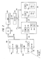
- Fig. 1 schematically shows an overall construction of a microcomputer system capable of performing a floating-point processing at a high speed, as an example of a coprocessor system, to which the present invention is applied. Therefore, the microcomputer system includes two processing units, i.e., central processing unit (CPU) 100 as a host processor and floating-point processing unit (FPU) 101 as a coprocessor.
- The
CPU 100 processes only integer data and does not carry out the processing of floating-point data. If theCPU 100 is made to process floating-point data, it has to be provided with software or programs to support such processing, so that the processing speed of the microcomputer system decreases as a whole. To prevent this, as already known, there is provided the FPU 101 which exclusively performs the processing of floating-point data at a high speed. - The microcomputer system is further provided with read-only memory (ROM) 102 and random-access memory (RAM) 103. The
ROM 102 stores programs including instructions to be executed by both theCPU 100 and the FPU 101. Since, however, instructions can be decoded only by theCPU 100, a high-speed interface is achieved by a protocol exclusively provided for the communication between theCPU 100 and the FPU 101. TheRAM 103 stores integer data and floating-point data to be processed and intermediate and final results of the processing. - The
aforesaid CPU 100, FPU 101,ROM 102 andRAM 103 of the microcomputer system are coupled with each other through three busses, i.e.,address bus 104,data bus 105 andcontrol bus 106. As usual, the microcomputer system further includes clock generator (CLKG) 107 for generating clock signals (CLK) supplied to theCPU 100, FPU 101,ROM 102 andRAM 103, however, for brevity, signal lines therefor are omitted in the figure. - Referring next to Fig. 2, there is shown the construction of the FPU 101 according to the embodiment of the present invention.
- As shown in this figure, there is provided in the FPU 101 bus control unit (BCU) 200, as an interface unit, for realizing a high-speed interface of the FPU 101 with other units or devices of the microcomputer system. Signals supplied to and derived from the
bus control unit 200 are as follows:
CLK: a clock signal supplied from theclock generator 107;
A: an address signal supplied from theCPU 100 through theaddress bus 104. This signal is a three bit signal, each bit being indicated by A2 to A0; and
D: data supplied from and derived to other units and devices through thedata bus 105. Data is composed of 32 bits, i.e., D31 to D0. - Further, as signals supplied to and derived from the
bus control unit 200 through thecontrol bus 106, there are the following:
CS : a chip select signal. If a device, other than the FPU 101, asserts this signal (i.e., makes a signal CS a low level), the FPU 101 is selected as a processing unit which carries out the data communication with the device;
AS : an address strobe signal indicating the existence of an address signal on theaddress bus 104;
DS : a data strobe signal indicating that data on thedata bus 105 is established;
R/W : a signal indicating the data transfer direction, which assumes "1" upon the read operation of theCPU 100 and "0" upon the write operation thereof;
DC : a signal indicating the completion of the data transfer through thedata bus 105. In the case of the data transfer between theCPU 100 and theFPU 101, this signal is outputted toCPU 100 from theFPU 101, when the data transfer is completed, and in the case of the data transfer between theFPU 101 and an external memory, theRAM 103, for example, this signal is inputted to theFPU 101 from the external memory, when the data transfer is completed;
CDE : a coprocessor data enable signal, which is supplied by theCPU 100 as an output timing signal. TheFPU 101 outputs a destination operand (processing result) onto thedata bus 105 in one clock cycle after this signal is asserted;
CPST: a signal indicating an internal operating status of theFPU 101. This signal is a three bit signal composed of CPST2 to CPST0; and
BAT: a signal indicating a kind of access made by theCPU 100. This signal is also a three bit signal composed of BAT2 to BAT0. - When the
FPU 101 receives the signal BAT from theCPU 100, it operates accordingly and returns to theCPU 100 the signal CPST indicating its internal status as the result of the operation. Thereby, the protocol is exchanged between theCPU 100 and theFPU 101. Codes and their meaning of the signal CPST are as follows:

- Further, codes and their meaning of the signal BAT are as follows:


- Moreover, the bus control unit (BCU) 200 includes command register (BCMR) 214, which stores a command issued by the
CPU 100 to be executed by theFPU 101. TheCPU 100 issues commands by decoding a floating-point processing instruction read out from theROM 102. - The
FPU 101 also includes format conversion unit (FCU) 201. Thisunit 201 communicates data with thebus control unit 200 throughdata bus 206 and converts the data in the external format into data of the internal format of theFPU 101, and vice versa. The external format data can be a signal precision format data, a double precision format data and a double-expanded precision format data, which are defined by the IEEE standard P754, for example. The internal format is determined in advance in one selected from among the aforesaid three formats, e.g., in the double-expanded precision format in this embodiment. - Although the format conversion of this sort is already known, an example of the format conversion will be explained briefly, with reference to Fig. 3. By way of example, assuming that external data taken in the
bus control unit 200 and outputted therefrom to theformat conversion unit 201 is of the single precision format (one bit for a sign, 8 bits for an exponent and 23 bits for a mantissa), theformat conversion unit 201 converts it into the double-extended precision format which is the internal format of theFPU 101, in the following manner. - At first, the 8-bit exponent portion in the signal precision format is converted into a form of 15 bits according to the aforesaid IEEE standard, whereby an exponent portion of the double-expanded precision format is formed. Then, the 23-bit mantissa portion of the signal precision format is put into a mantissa portion of the double-expanded precision format by successively stuffing it from the left-end bit and filling all the remaining bits with "0" so as to form the mantissa portion of total 63 bits.
- In the case where data of an
execution unit 202, which will be described later, is to be transferred to thebus control unit 200, theformat conversion unit 210 converts the data format from the internal format (the double-expanded precision format) to the external format as specified by means of the reverse conversion of the above mentioned conversion. - The
format conversion unit 201 is provided with the following registers, i.e., command register (FCMR) 212, instruction address register (FIAR) 213, input register (FIR) 219 and output register (FOR) 220. Thecommand register 212 stores a command which is issued by theCPU 100 and executed by theFPU 101. Contents of thisregister 212 means a command which uses data converted by theformat conversion unit 201. - The instruction address register 213 stores an instruction address issued by the
CPU 100. This instruction address is used for the following purpose. In a processor which does not carry out the pipeline processing, if the processor anomalously stops operating, it can be easily recognized that the anomalous stop is caused by a command under execution, because only one instruction is executed at that time. On the other hand, however, plural instructions are simultaneously executed in a processor which carries out the pipeline processing. An instruction address is used in order to identify which command causes the anomalous stop. Therefore, an instruction address is necessary to attend every command in the pipeline processing system. - The input register 219 stores data of the internal format, which is converterd from data of the external format, and the
output register 220 stores data, which is obtained by converting internal format data into one of the external formats as designated. - The
FPU 101 includes an execution unit (EU) 202, which receives converted internal format data from theformat conversion unit 201 and executes a predetermined processing to perform a floating-point operation. Theexecution unit 202 is provided with floating-point registers (FR0 to FR7), composed of 8 words, for storing data used for the operation and the result of operation, and temporary registers (TR0 to TR7), which is also composed of 8 words and temporarily store intermediate results of the operation. - The
execution unit 202 is further provided with command register (ECMR) 217 and instruction address register (EIAR) 218. The former stores a command issued by theCPU 100 and executed by theexecution unit 202 and the latter stores an instruction address of a command issued by theCPU 100. In addition to the registers as mentioned above, theexecution unit 202, as usually known, includes an arithmetic logic unit, barrel shifters and multipliers. - The
FPU 101 includesROM 203, in which a microprogram for executing the floating-point processing is stored. Instruction executing codes read out from theROM 203 are decoded bydecoder 204, whereby control signals 210 and 211 are generated. These control signals 210 and 211 are applied to theexecution unit 202 and theformat conversion unit 210 to control them, respectively. - The reading-out of the instruction executing codes from the
ROM 203 is controlled by signals frominstruction sequencer 205, to which a command, which is issued by theCPU 100 and received by thebus control unit 200, is given throughinstruction bus 208. - Referring next to Fig. 4, explanation will be made of the pipeline processing carried out in the
FPU 101 and its operational timing. This figure shows a flow from a k-th command CMDk to a (k+2)-th command CMDk+2. - The command CMDk and its operand OPSk and instruction address IARk, which are transferred from the
CPU 100, are successively inputted to the bus control unit (BCU) 200 through thedata bus 105 for every bus cycle B1 to B3. Among those, the command CMDk is inputted to theinstruction sequencer 205 through thebus 208, wherebyinstruction executing codes 209 are read out from theROM 203 in accordance with the command CMDk, and they are decoded in thedecoder 204 to produce the control signals 211, 210 for theformat conversion unit 201 and theexecution unit 202. - The operand OPSk is further inputted to the format conversion unit (FCU) 201 through the
bus 206 in the bus cycle B3. The operand OPSk is subject to the format conversion in thisunit 201. - The format-converted operand OPSk is transferred to the
execution unit 202, in which the execution of the command CMDk is commenced and carried out through the bus cycles B4 to B6. On the other hand, at the same time as the commencement of the execution of the command CMDk, the next, i.e., (k+1)-th, command CMDk+1 starts to be fetched in the bus cycle B4. - In this manner, by controlling the operation of the
bus control unit 200, theformat conversion unit 201 and theexecution unit 202 on the pipeline processing basis, the results of execution of the (k-1)-th command CMDk-1, the k-th command CMDk and the (k+1)-th command CMDk+1 can be obtained by the ends of the bus cycles B3, B6 and B9, respectively. - Further, in the example as mentioned above, there is shown the case where a source operand is in a memory and a destination operand is in a register.
- As described above, the
FPU 101 usually carries out the pipeline processing that thebus control unit 200, theformat conversion unit 201 and theoperation unit 202 are operated independently from each other, in order to realize the high speed processing. To this end, the threeunits - Further, the
format conversion unit 201 and theexecution unit 202 are provided with the instruction address registers 213 and 218 for storing instruction addresses of current commands executed by theunits - Now, the operation when a save command FSAVE is executed, will be described, referring to Fig. 5, in which there is shows a flow chart of the operation of the
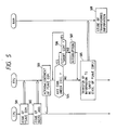
CPU 100, theFPU 101 and theRAM 103. - The command FSAVE performs the processing of transferring an internal status or information of the
FPU 101 to external resources such as theRAM 103. Namely, for example, the command FSAVE carries out the saving of the internal status of theFPU 101 in order to analyze a task switch or an anomalous (exceptional) stop, as described below. - To switch a task A being executed by the
FPU 101 at present to another task B. When an operating system (OS) for managing a whole system switches over the task A to the task B, the OS issues a save command FSAVE in order to save intermediate results of the processing of the task A from theFPU 101 to theRAM 103. Further, when the task A is executed again, a restore command FREST is issued in order to restore the saved intermediate results into theFPU 101. - When the
FPU 101 stops because of an exceptional cause, data of registers of theFPU 101 are transferred to theRAM 103 by a save command FSAVE, and the saved contents of theRAM 103 are referred to, in order to analyze the cause. - In the cases as mentioned above, the internal status of the
FPU 101 can not be transferred to theRAM 103 by a transfer instruction provided for general cases. A command provided for coping with this is a save command FSAVE. If, however, theFPU 101 is under execution of any other command, it can not start to execute a save command FSAVE. - Therefore, a time from receipt of a command FSAVE to start of execution thereof greatly depends on the condition of the
FPU 101 when the command FSAVE is received, i.e., theFPU 101 is in the interrupted condition or under the operation, and further in the latter case, theFPU 101 just starts the execution of a new command or ends it soon, when the command FSAVE is received. Accordingly, a time necessary for theCPU 100, which issues a command FSAVE, to confirm the acknowledgment thereof varies very much, and in the worst case, theCPU 100 is forced to be in the waiting condition for a long time. - To prevent this, the saving operation according to the present invention is performed as follows. At first, as shown in Fig. 5, the
CPU 100 issues a save command FSAVE and its instruction address to the FPU 101 (steps 501, 502). When theFPU 101 confirms that a command sent from theCUP 100 is a save command FSAVE, it immediately receives the command unconditionally, whether thebus control unit 200, theformat conversion unit 201 and theexecution unit 202 are under operation or not. Then, theFPU 101 acknowledges the command FSAVE to theCPU 100 by means of the signal CPST (step 503). - However, the start of execution of the command FSAVE depends on the internal status of the
execution unit 202 of theFPU 101 and the attribute of a command executed by theFPU 101 at that time. The relationship therebetween is represented in the table 1 below.Table 1 Status of the unit 202Execution of FSAVE idle started at once exceptional status ditto under execution of commands FREM, FMOD, FSIN, FCOS, FTAN or FSINCOS ditto under execution of other commands started after completion of execution of a command under execution - In the table above;
FREM: IEEE modulo calculation instruction;
FMOD: modulo calculation instruction;
FSIN: sine conversion instruction;
FCOS: cosine conversion instruction;
FTAN: tangent conversion instruction; and
FSINCOS: sine and cosine conversion instruction. - Further, although there are used both terms "command" and "instruction" in the foregoing description, they can be considered to express substantially the same here. The term "instruction" is an expression, when viewed from the
CPU 100 or an operator's standpoint, and the term "command" is an expression, when viewed from theFPU 101. - Among commands for the floating-point processing executed by the
FPU 101, the commands FREM, FMOD, FSIN, FCOS, FTAN and FSINCOS as mentioned above belong to a group of commands which require a relatively long processing time. We will call a command of this group "a long command" for the convenience of the following explanation. If theFPU 101 receives a save command FSAVE during the execution of a long command, it interrupts the execution of the long command and starts the execution of the command FSAVE. At this time, of course, intermediate results of execution of the long command must be saved together with the internal status of theexecution unit 202. - A command other than the aforesaid commands will be called "a short command". As a short command, there are various kinds of general operation commands such as FADD (add), FSUB (subtract), FMUL (multiply), FDIV (divide), FSCALE (scale), FABS (find absolute), FNEG (find negative), FSQRT (find square root), FINT (infinite), FINTRZ (extract mantissa), as well as commands for coordinates conversion, judgment, branch, transfer and other processings.
- The aforesaid various commands has been enumerated only for the purpose of exampling the long command and the short command. It is to be noted that all commands to be executed by the
FPU 101 can be arbitrarily classified into two categories, i.e., a short command group or a long command group, in accordance with a predetermined criterion. Generally, a command including the repetitive operation, such as a command used in a calculation of approximation, will belong to a long command. - Returning to Fig. 5, after acknowledgment of the save command FSAVE (step 503), the
FPU 101 discriminates whether or not there is any command under execution (step 504). If there is no command under execution, the processing of theFPU 101 goes to step 505. If there is any command under execution, it is further discriminated whether or not the command is a short command (step 506). This discrimination can be carried out on the basis of the classification or categorization of commands as mentioned above. - If the command under execution is discriminated to be a short command, steps 504 and 506 are repeatedly executed, until it is judged at
step 504 that there is no command under execution. If it is judged atstep 506 that the command under execution is discriminated to be no a short command, i.e., in the case where the command under execution is a long command, the execution of the long command is interrupted (step 507) and then the processing of theFPU 101 goes to step 505. - At
step 505, theFPU 101 executes the command FSAVE, whereby information to be saved is formed based on the internal status of theFPU 101 and transferred to theRAM 103. TheRAM 103 stores the transferred information (step 508). With this, the saving of the information within theFPU 101 is completed. - In the following, the formation of the information to be saved will be explained. Various indexes indicating the internal status of the
FPU 101 and a word count (WS) indicating an amount of information to be transferred are included in a first word of the information to be transferred. This first word is called "a frame header (FH)", hereinafter. The construction of the frame header FH is as shown in Fig. 6. - The frame header FH includes a coprocessor identification COP.ID of three bits. In the case where a coprocessor system includes plural coprocessors, every coprocessor has a particular identification COP.ID. Therefore, it can be identified by this COP.ID. which coprocessor originates the information to be saved. An index EX of two bits, represented by EX1 and EX0, indicates three kinds of the status of the
execution unit 202, as follows.EX1 EX0 Status of the unit 2020 0 idle 0 1 reserved 1 0 interruption processing 1 1 exception - In the above, "idle" means the status that the
execution unit 202 completes the execution of a command and stops to wait for a next command. "Interruption processing" means the status that since theFPU 101 receives a save command FSAVE during the execution of a long command, it interrupts the processing of the long command and stops. "Exception" means the status that the execution of theFPU 101 is interrupted because of occurrence of anomalies and exceptions such as overflow, underflow, division by zero, and further execution becomes impossible. - An index OPL of one bit indicates whether or not a command unexecuted exists in the
FPU 101. If OPL assumes "1", this means that there still exists a command unexecuted, although theFPU 101 completes to exchange a protocol with theCPU 100. These two indexes EX and OPL as mentioned above are important as indexes representing the internal status of theFPU 101 upon receipt of a save command FSAVE. - An index EXCO of one bit, which has the meaning only in the case of "exception", i.e., (EX1, EX0) = (1, 1), indicates that an operand used for the execution among the information saved by execution of the command FSAVE is bias-regulated by the
format conversion unit 201. An index FIRRQ of one bit indicates that an unexecuted command in theFPU 101 has an operand. Accordingly, only when OPL representing the existence of an unexecuted command is set, FIRRQ is set. - The word count (WC) indicates a number of words of information to be saved, excluding the frame header FH. An amount of information to be saved is made variable in accordance with the internal status of the
FPU 101 represented by the indexes EX (EX1, EX0) and OPL, whereby the transfer of unnecessary information is prevented. The relationship of EX (EX1, EX0), OPL and the word count (WC) is indicated in the table 2 below.Table 2 EX1 EX0 OPL WC (words) 0 0 0 0 0 0 1 5 1 0 0 26 1 0 1 31 1 1 0 26 1 1 1 31 - A value of WC indicated above does not include the frame header FH. Therefore, the number of words to be actually transferred is by one word more than the value indicated in the table.
- If the correspondence between EX1, EX0, OPL and WC is provided as a table in advance, the occurrence of error in the data transfer can be easily checked by counting a number of words actually transferred and referring to the table.
- In the following, explanation will be made of the timing of operation of the
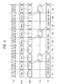
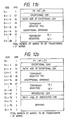
CPU 100 and theFPU 101, as well as contents of information to be transferred, an order of transfer and addresses of theRAM 103, at which the information to be saved is stored, referring to Figs. 7a, 7b to 12a, 12b. - By the way, when the
FPU 101 is going to execute a save command FSAVE, its internal status can assume six kinds of status, which are represented by the combination of EX1, EX0 and OPL (it is to be noted that (EX1, EX0) = (0, 1) is reserved). Among the figures, Figs. 7a, 8a, ..., 12a show the execution timing of theCPU 100 and theFPU 101 for each of the aforesaid six kinds of the status, and Figs. 7b, 8b, ..., 12b show the contents of information to be transferred, the order of transfer (ORD) and the allocation of addresses (ADD) of theRAM 103. - Referring at first to Fig. 7a, there is shown the timing of execution, in the case where when a save command FSAVE is issued by the
CPU 100, theFPU 101 is idle ((EX1 , EX0) = (0, 0)) and there is no unexecuted command (OPL = 0). Namely, before issuance of the command FSAVE, the bus control unit (BCU) 200, the format conversion unit (FCU) 201 and the execution unit (EU) 202 of theFPU 101 are all idle. Therefore, when the command FSAVE and its instruction address IARk are issued by theCPU 100, they are taken in theFPU 101 through the BCU, and the command FSAVE is executed at once. - In this case, only the frame header FH with WC = 0, as shown in Fig. 7b, is transferred to the location of address $n of the
RAM 103. Any other information is not transferred. Therefore, the total number of words to be transferred is only one word. - Fig. 8a is a timing chart of the execution under the condition that when the
CPU 100 issues a save command FSAVE, theFPU 101 is idle ((EX1, EX0) = (0, 0)), but there exists a command unexecuted (OPL = 1). More particularly, before issuing the command FSAVE, theCPU 100 issues a command CMDk as well as its operand OPSk and instruction address IARk and transfers them to theFPU 101. At this time, in theFPU 101, the FCU initiates the format conversion of the operand OPSk, however the EU still keeps the status at the time of the execution of a previous command CMDk-1 and therefore does not start to execute the command CMDk yet. Namely, the command CMDk remains unexecuted at this time. - Fig. 8b shows the contents of information to be transferred and the order of transfer as well as the allocation of addresses of the
RAM 103 in this case. As shown in the figure, the contents of information to be saved from theFPU 101 to theRAM 103 include the frame header FH as well as the unexecuted command CMDk and its instruction address IARk and operand OPSk. - The word count WC of the frame header FH in this case assumes 5, and this means that five words are transferred, in addition to the frame header FH itself. The unexecuted command CMDk and its instruction address IARk and operand OPSk are held in the
command register 212, theinstruction address register 213 and the input register 219 of theformat conversion unit 201, respectively. - As already described, although the operand OPSk, when it is issued from the
CUP 100, is of the external format (the single precision format), it is converted into the internal format (the double-precision format) by theformat conversion unit 210 and stored in theinput register 219. Therefore, an area of three words is prepared for the operand OPSk, as shown in Fig. 8b. - The
FPU 101 transfers the information of the contents as mentioned above to theRAM 103 in the following order. At first, the frame header FH is transferred to the location of address $n of theRAM 103. Next, the operand OPSk of the internal format is transferred to the locations of addresses $n+14, $n+10 and $n+C of theRAM 103. - Thereafter, the instruction address IARk of the unexecuted command CMDk is transferred to the location of address $n+8 of the
RAM 103, and lastly the unexecuted command CMDk is transferred to the location of address $n+4 of theRAM 103. - Referring next to Fig. 9a, there is shown a timing chart of the execution under the condition that when the
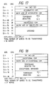
CPU 100 issues a save command FSAVE, theFPU 101 is in the interruption processing ((EX1, EX0) = (1, 0)), but there is no command unexecuted (OPL = 0). More particularly, theCUP 100 issues a command FSIN for calculating a sine function as well as an operand OPSk and instruction address IARk thereof, and transfers them to theFPU 101. - In the
FPU 101, after receipt of them in the BCU, the FCU converts the format of the operand OPSk and then the EU starts the execution of obtaining a sine value with respect to the format-converted operand OPSk. Under those circumstances, if theCPU 100 issues a save command FSAVE during the execution of the command FSIN, theFPU 101 receives the save command FSAVE and starts the execution thereof after interruption of the execution of the command FSIN, because the command FSIN belongs to the long command. In this case, the command FSIN is called an interrupted command. - Fig. 9b shows the contents of information to be transferred and the order of transfer as well as the allocation of addresses of the
RAM 103, for the purpose of executing the command FSAVE under the condition as mentioned above. - As shown in the figure, the contents of information to be saved from the
FPU 101 to theRAM 103 include the frame header FH, the interrupted command FSIN and its instruction address IARk as well as contents of the temporary registers TR0 to TR7 of the EU. - The word count WC of the frame header FH in this case assumes 26, and this means that further 26 words are transferred in addition to the frame header FH itself. The interrupted command FSIN and its instruction address IARk are held in the
command register 217 and theinstruction address register 218 of theexecution unit 202, respectively. Further, the temporary registers TR0 to TR7 hold the intermediate results of the interrupted execution of the command FSIN. - The
FPU 101 transfers the information of the contents as mentioned above to theRAM 103 in the following order. First of all, the frame header FH is transferred to the location of address $n of theRAM 103. Next, contents of the temporary register TR7 are transferred to the locations of addresses $n+68, $n+64 and $n+60 of theRAM 103, and then contents of the temporary registers TR6 to TR0 are successively transferred to the locations of respectively allocated addresses, as shown in Fig. 9b. - Thereafter, the instruction address IARk of the interrupted command FSIN is transferred to the location of address $n+8 of the
RAM 103, and lastly, the interrupted command FSIN is transferred to the location of address $n+4. - Next in Fig. 10a, there is shown a timing chart of the execution under the condition that when the
CUP 100 issues a save command FSAVE, theFPU 101 is in the interruption processing ((EX1, EX0) = (1, 0)) and there is an command unexecuted (OPL = 1). Similarly to the case as mentioned above, a command FSIN belonging to the long command will be taken as an example. - The
CPU 100 issues a command FSIN as well as operand OPSk and instruction address IARk thereof, and transfers them to theFPU 101. Then, theCPU 100 successively issues a command CMDk+1 and its operand OPSk+1 and instruction address IARk+1 and transfers them to theFPU 101. - In the
FPU 101, after receipt of the command FSIN and its accessories in the BCU, the FCU converts the format of the operand OPSk and then the EU starts the execution of obtaining a value of the sine function with respect to the format-converted operand OPSk. During the execution of the command FSIN by the EU, the BCU receives the command CMDk+1 and its accessories, and then the FCU performs the format-conversion of the operand OPSk+1. At this time, the EU continues to execute the command FSIN. - Under these circumstances, if the
CUP 100 issues a save command FSAVE and its instruction address IARk+2, theFPU 101 receives them and starts the execution of the command FSAVE after interruption of the execution of the command FSIN by the EU. Therefore, the received command CMDk+1 remains unexecuted. Namely, in this case, the command FSIN is an interrupted command and the command CMDk+1 is an unexecuted command. - There are shown in Fig. 10b the contents of information to be transferred and the order of transfer as well as the allocation of addresses of the
RAM 103, for the purpose of executing the command FSAVE under the condition as mentioned above. - As shown in this figure, the contents of information to be saved from the
FPU 101 to theRAM 103 include the frame header FH, the interrupted command FSIN, its instruction address IARk, contents of the temporary registers TR0 to TR7 of theexecution unit 202, the unexecuted command CMDk+1 and its instruction address IARk+1 and operand OPSk+1. The total number of words to be transferred amounts to 32 words. - The word count WC of the frame header FH in this case assumes 31 and indicates that there are further 31 words to be transferred, in addition to the frame header FH. The interrupted command FSIN and its instruction address IARk are held in the
command register 217 and theinstruction address register 218 of theexecution unit 202, respectively. The temporary registers TR0 to TR7 hold intermediate results of the interrupted execution of the command FSIN. - Further, the unexecuted command CMDk+1 and its instruction address IARk+1 are held in the
command register 212 and theinstruction address register 213 of theformat conversion unit 210. The operand OPSk+1 thereof is held in the input register 219 of theformat conversion unit 210 in the converted format of three words. - The
FPU 101 transfers the information of the contents as mentioned above to theRAM 103 in the following order. First of all, the frame header FH is transferred to the location of address $n of theRAM 103. Next, the format-converted operand OPSk+1 of the unexecuted command CMDk+1 are transferred to the locations of addresses $n+7C, $n+78 and $n+74 of theRAM 103. Then, the instruction address IARk+1 and the unexecuted command CMDk+1 are transferred to the locations of addresses $n+70 and $n+6C. - Further, contents of the temporary registers T0 to TR7 are transferred to the locations of addresses $n+68 to $n+C of the
RAM 103. Thereafter, the instruction address IARk of the interrupted command FSIN is transferred to the location of address $n+8 of theRAM 103, and lastly, the interrupted command FSIN is transferred to the location of address $n+4 of theRAM 103. - Fig. 11a is a timing chart of the execution under the condition that when the
CPU 100 issues a save command FSAVE, theFPU 101 is in the exceptional status ((EX1, EX0) = (1, 1)), but there is no command unexecuted (OPL = 0). - The
CPU 100 issues a command CMDk and its operand OPSk and instruction address IARk, and transfers them to theFUP 101 one after another. In theFPU 101, the BCU receives them and the FCU converts the format of the operand OPSk. The EU starts the execution of the command CMDk with respect to the format-converted operand OPSk. During the execution of the command CMDk, however, the EU can no longer continue the execution and stops because of occurrence of the exception such as overflow. When theFPU 101 is in this status, theCPU 100 issues a save command FSAVE and its instruction address IARk+1. In this case, the command CMDk is called an exceptional command, hereinafter. - There are shown in Fig. 11b the contents of information to be transferred and the order of transfer as well as the allocation of addresses of the
RAM 103, for the purpose of executing the command FSAVE under the condition as mentioned above. - As shown in this figure, the contents of information to be saved from the
FPU 101 to theRAM 103 include the frame header FH, the exceptional command CMDk and its instruction address IARk and operand OPSk. Hereinafter, the last two will be called an exceptional instruction address and an exceptional operand, respectively. Further, the microprogram 203 (cf. Fig. 2) is programed so as to always store the exceptional operand OPSk in the temporary register TR0. The information to be transferred further includes contents of the temporary registers TR7 to TR1, which are in fact empty. In this case, the total number of words to be transferred amount to 27 words, including the frame header FH. - The word count WC of the frame header FH in this case assumes 26 and indicates that there are further 26 words to be transferred, in addition to the frame header FH. The exceptional command CMDk and its instruction address IARk are stored in the
command register 217 and theinstruction address register 218 of theexecution unit 202, respectively. In the exceptional operand OPSk, there exists data which caused the exception. Although the contents of the temporary registers TR7 to TR1 are transferred, they have no special significance. - The order of transfer of the information as mentioned above is as follows. As shown in Fig. 11b, first of all, the frame header FH is transferred to the location of address $n of the
RAM 103. Then, the contents of the temporary registers TR7 to TR1 are transferred to the locations of addresses $n+68 to $n+18 of theRAM 103, however, as already described, they have no special significance. Next, the contents of the temporary register TR0 are transferred to the location of addresses $n+14 to $n+C as the exceptional operand. - Thereafter, the instruction address IARk of the exceptional command CMDk is transferred to the location of address $n+8 of the
RAM 103, and lastly the exceptional command CMDk is transferred to the location of address $n+4 of theRAM 103. - Referring lastly to Fig. 12a, there is shown a timing of the execution under the condition that when the
CUP 100 issues a save command FSAVE, theFPU 101 is in the exceptional status ((EX1, EX0) = (1, 1)) and there is a command unexecuted (OPL = 1). - The
CPU 100 issues a command CMDk and its operand OPSk and instruction address IARk, and transfers them to theFPU 101. Then, a next command CMDk+1 and its operand OPSk+1 and instruction address IARk+1 are issued and transferred to theFPU 101. - In the
FPU 101, after the BCU receives the command CMDk and its accessories, the FCU converts the format of the operand OPSk. The EU executes the command CMDk, using data of the operand OPSk. During the EU executes the command CMDk, the BCU receives the command CMDk+1 and its accessories, and the operand OPSk+1 thereof is subject to the format-conversion in the FCU. In the example shown, the exceptional status occurs during the execution of the command CMDk, whereby the execution becomes no longer possible and the EU stops. Under those circumstances, theCPU 100 issues the command FSAVE and its instruction address IARk+2. In this case, the command CMDk becomes an exceptional command and the command CMDk+1 becomes an unexecuted command. - There are shown in Fig. 12b the contents of information to be transferred and the order to transfer as well as the allocation of addresses of the
RAM 103 in the execution of the command FSAVE under the condition as mentioned above. - As shown in the figure, the contents of information to be saved from the
FPU 101 to theRAM 103 include the frame header FH, the exceptional command CMDk and its instruction address IARk and operand OPSk. Also in this case, the last two are called an exceptional instruction address and an exceptional operand, respectively. Further, the exceptional operand OPSk is held in the temporary register TR0. The information to be transferred further includes the unexecuted command CMDk+1 and its instruction address IARk+1 and operand OPSk+1 as well as insignificant contents of the temporary registers TR7 to TR1. The total number of words to be transferred amounts to 32 words. - As shown in Fig. 12b, the word count WC of the frame header FH in this case assumes 31 and indicates that there are further 31 words to be transferred, in addition to the frame header FH. In the same manner as that in Fig. 10b, the unexecuted command CMDk+1 is a command which remained unexecuted because of occurrence of the exception, although it was received by the
FPU 101. Its instruction address IARk+1 and operand OPSk+1 are also the same as those in Fig. 10b. - Also, the exceptional command CMDk, the exceptional instruction address IARk and the exceptional operand OPSk as well as the insignificant contents of the temporary registers TR7 to TR1 are the same as those shown in Fig. 11b.
- The order to transfer of the information as mentioned above is as follows. As shown in Fig. 12B, first of all, the frame header FH is transferred to the location of address $n of the
RAM 103. Next, the unexecuted operand OPSk+1 is transferred to the location of addresses $n+7c to $n+74 of theRAM 103, and then the unexecuted instruction address IARk+1 and the unexecuted command CMDk+1 are successively transferred to the locations of addresses $n+70 and $n+6C, respectively. - After that, the insignificant contents of the temporary registers TR7 to TR1 are transferred to the locations of addresses $n+68 to $n+18 of the
RAM 103. The contents of the temporary register TR0 are transferred to the location of addresses $n+14 to $n+C as the exceptional operand. - Lastly, the exceptional instruction address IARk and the exceptional command CMDk are transferred to the locations of addresses $n+8 and $n+4 of the
RAM 103, respectively. - As described above, when the
FPU 101 receives a save command FSAVE, it discriminates, in accordance with the status of theexecution unit 202 and the category of a current command under execution, whether theFPU 101 interrupts the execution of the current command and starts the processing of the command FSAVE or whether it continues the execution of the current command and has the processing of the command FSAVE waiting. Therefore, the saving operation of theFPU 101 becomes possible according to the status of theFPU 101. - Further, the information to be saved includes the coprocessor identification COP.ID, the word count WC and various indexes, such as EX and OPL, representing the internal status of the
FPU 101, in addition to contents of registers, which hold intermediate results of the processing within theFPU 101. With this, the restoring operation, which will be described later, can be performed in safe and reliably. - Although it has already stated that the
FPU 101 unconditionally receives a save command FSAVE issued by theCPU 100, the reasons therefor are as follows. As a manner of receiving a save command FSAVE in theFPU 101, there can be considered the following two cases: - 1) after receiving a save command FSAVE, the
FPU 101 prepares itself for the execution thereof (unconditional receipt of a save command FSAVE); and - 2) before receiving a save command FSAVE, the
FPU 101 prepares itself for the execution thereof. - In the embodiment described above, as measures for reducing a time necessary for preparing the execution of a save command FSAVE, a current command under execution upon receipt of the command FSAVE continues to be executed and the execution of the command FSAVE is waited, if the current command is a short command. On the contrary, if the current command is a long command, the execution thereof is interrupted and the command FSAVE starts to be executed at once.
- In the
FPU 101, which adopts such measures for reducing the preparing time, the measures becomes much more effective, if theFPU 101 prepares itself for the execution of a save command FSAVE after receiving it, as described in the case 1) above. Therefore, the unconditional receipt of a save command FSAVE is adopted in the embodiment. However, it is to be noted that the present invention is never limited to the unconditional receipt of a save command FSAVE. - Now, the information, which has been once saved in the
RAM 103, must be restored in theFPU 101 again, when theFPU 101 restarts the execution of an unexecuted command, an interrupted command and/or an exceptional command. In the following, description will be made of the restoring operation of the saved information to theFPU 101. - A command, which is used in order to restore the saved information from the
RAM 103 to theFPU 101 again, is called a restore command FREST. Therefore, the operation of execution of a restore command FREST will be described, hereinafter. The process of execution of a restore command FREST is shown by a flow chart of Fig. 13. - At first, the
CPU 100 issues a restore command FREST to the FPU 101 (step 1301). The issuance of the command FREST is managed by a program of the operating system of the coprocessor system. After issuing the command FREST, theCPU 100 instructs theRAM 103 to transfer a frame header FH to the FPU 101 (step 1302). The frame header FH transferred in this time is the same as the frame header, which is transferred to theRAM 103 as one of the information to be saved and therefore has the same structure as shown in Fig. 6. - The
FPU 101 can receive the command FREST, only when it is idle. Therefore, theFPU 101 discriminates its own internal status (step 1303) and sends the discrimination result to theCPU 100 as the signal CPST. - If there remains an unexecuted command or a command under execution within the
FPU 101, i.e., if the discrimination result atstep 1303 is "no", theFPU 101 judges that the command FREST can not be received and requests theCPU 100 to reissue the command FREST (step 1305). In response to this request, theCPU 100 instructs theRAM 103 to retransfer the frame header FH, again. This operation is repeated, until the unexecuted command or the command under execution is completed to be executed, i.e., until the result in the discrimination atstep 1303 changes to "yes". - If an command within the
FPU 101 is completely executed, theFPU 101 acknowledges the command FREST to the CPU 100 (step 1304). In response thereto, theCPU 100 issues an instruction address of the command FREST to theFPU 101. Then, theFPU 101 checks the number of transfer words by comparing a value of the word count WC with the combination of the indexes EX (EX1, EX0) and OPL, of the frame header FH transferred from the RAM 103 (step 1307). - If the relationship between the combination of EX (EX1, EX0) and OPL and the word count WC meets the correspondence as presented in the table 2, the number of transfer words is judged to be normal and the
FPU 101 informs theCPU 100 thereof (step 1308), and otherwise theFPU 101 informs theCPU 100 that the number of transfer words is abnormal (step 1309). - In the case where the
CPU 100 is informed that the number of transfer words is normal, theCPU 100 instructs theRAM 103 to transfer the remaining part of the information saved by the execution of a save command FSAVE. In response to this instruction, theRAM 103 transfers the information to be restored to the FPU 101 (step 1310). At this time, theFPU 101 can recognize the format and contents of the transferred information from the contents of the frame header FH and therefore store them in corresponding registers of theFPU 101. - Further, it is to be noted that the frame header FH is transferred at first both in a save command FSAVE and in a restore command FREST, however the order to transfer of the remaining words is different in the latter from in the former. In this manner, by transferring the frame header FH first and checking the correctness thereof, the erroneous restoring operation can be prevented.
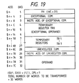
- Fig. 14 shows contents of information to be restored in the
FPU 101 in the case of (EX1, EX0) = (0, 0) and OPL = 0 in the frame header FH. Namely, this corresponds to the case of the saved information described with reference to Figs. 7a and 7b. This figure also indicates an order of transfer (ORD) and an address (ADD) of theRAM 103, from which the information to be restored is read out. In this case, as shown in the figure, the word count WC of this frame header FH is zero, which indicates that an information to be restored is the frame header FH only. - Fig. 15 shows contents of information to be restored in the
FPU 101 in the case of (EX1, EX0) = (0, 0) and OPL = 1. Therefore, this corresponds to the case of the saved information described with reference to Figs. 8a and 8b. Since the word count WC in this case is 5, the total number of transfer words amounts to 6 words. - The order of transfer is as follows. The frame header FH, which is read out from the address $n of the
RAM 103, is at first transferred. Then, the unexecuted command read out from the address $n+4 of theRAM 103 and the instruction address read out from the address $n+8 are transferred to theFPU 101 successively. Lastly, the operand read out from the addresses $n+C to $n+14 of theRAM 103 are transferred to theFPU 101 in the order as shown. - Fig. 16 shows contents of information to be restored in the
FPU 101 in the case of (EX1, EX0) = (1, 0) and OPL = 0. This corresponds to the case of the saved information described with reference to Figs. 9a and 9b. As shown in the figure, the word count WC in this case amounts to 26 and therefore the total number of transfer words amounts to 27 words. Also in this case, the frame header FH is at first transferred to theFPU 101. Although the order of transfer is different, the contents to be transferred are the same as those as shown in Fig. 9b. - As described above, in all cases, the frame header is at first transferred to the
FPU 101 both in the transfer from theFPU 101 to theRAM 103 and in the transfer from theRAM 103 to theFPU 101. Also the contents of information to be transferred are the same in both the transfer directions. Only the difference therebetween is in the order of transfer. Therefore, the restoring operation as shown in Figs. 17 to 19, which correspond to Figs. 10b to 12b, respectively, can be easily understood. - In this manner, by executing a restore command FREST , the
FPU 101 can recover the status according to the contents of the information restored, which corresponds to the status before the execution of a save command FSAVE. The table 3 indicates the relationship of the values of EX1, EX0 and OPL within the frame header FH, the FPU status to be restored by the FREST command and the FPU status just after the execution of the FREST command. - As indicated in the Table 3, when the execution of a restore command FREST is completed, the
FPU 101 can restart the execution from a point, at which the execution thereof is interrupted by the command FSAVE.Table 3 Value of Frame Header FPU status to be restored by FREST FPU status just after FREST execution Unexecuted Command Execution Unit Unexecuted Command Execution Unit EX1 EX0 OPL Yes/No State Yes/ No State 0 0 0 No Idle No Idle 0 0 1 Yes Idle No Execution start 1 0 0 No Processing No Execution restart 1 0 1 Yes Processing Yes Execution restart 1 1 0 No Exception No Exception 1 1 1 Yes Exception Yes Exception - Further, the following use of the frame header FH can be considered.
- 1) In the case where a save command FSAVE is issued during a coprocessor stops due to the exception, a frame header of an information to be saved in an external memory has (EX1, EX0) = (1, 1). When the saved information is restored, although the frame header is usually transferred to the coprocessor with the same value of (EX1, EX0), it can be also restored with (EX1, EX0) changed to (0, 0), for example. With this, the coprocessor can restart the processing from the point at which it stops.
- 2) In a coprocessor system including plural coprocessors, a frame header of an information saved from a coprocessor is restored with a coprocessor identification COP.ID changed to that of another coprocessor.
- According to the embodiment, because when a saved information is restored in the
FPU 101, theFPU 101 judges whether or not a restore command FREST can be received properly, i.e., theFPU 101 is idle, and further the restoring operation is carried out after checking the word count, the erroneous operation caused by restoring erroneous information to theFPU 101 can be prevented. - By the way, there is the following relationship between a time point, at which a save command FSAVE starts to be executed, and a time necessary for executing the FSAVE command. Here it is assumed that the
CPU 100 issues a save command FSAVE during theFPU 101 executes a current command. - Under those circumstances, if the
FPU 101 interrupts the execution of the current command and starts to execute the command FSAVE at once, there may occur a large amount of intermediate results of the interrupted execution of the current command, according to a point, at which the execution of the current command is interrupted. In this case, a large amount of information must be transferred to theRAM 103 by executing the command FSAVE. This fact requires a long time for the execution of not only a save command FSAVE, but also a restore command FREST which will be executed later. - On the contrary, if the FSAVE command starts to be executed after the execution of the current command is completed, there are no intermediate results as the information to be transferred to the
RAM 103 by execution of the command FSAVE. In this case, since only a frame header FH is transferred, the time necessary for executing the command FSAVE becomes very short. Further, since an amount of the information saved is small, the time necessary for execution of a restore command FREST is short, too. - Accordingly, a time point of starting the execution of a save command FSAVE and a time necessary for executing the command FSAVE result in a problem of trade-off between both. In the embodiment as described above, as the solution of this problem, commands are classified into two categories, i.e., a short command group and a long command group, according to a time necessary for the execution thereof, and the execution of a command is interrupted only when a command under execution upon receipt of a save command FSAVE belongs to a long command.
- In order to further reduce an amount of information to be communicated between the
FPU 101 and theRAM 103, the following improvement can be considered. According to the inventors' analysis, an amount of information (intermediate results), which occurs in the course of the execution of a command in theFPU 101, varies so as to repeatedly increase and decrease as a time from the start of execution of the command proceeds, and there are some points (i.e., steps in the process of execution of the command), at which the amount of the intermediate results becomes very small. - If, therefore, some markers are provided in advance at such points in a command and the
FPU 101 interrupts the execution when detecting such a marker after receipt of a save command FSAVE, the start of execution of the command FSAVE is not delayed so much and the time necessary for executing the command FSAVE does not become long. With this, the effect of the present invention is much enhanced. - In the embodiment mentioned above, there has been used a RAM as an external memory which stores information to be saved. However, a special memory for that purpose can be provided within a processor. If a cache memory is provided, the high speed saving or restoring operation becomes possible.
- Moreover, in the foregoing, the present invention has been described with respect to a coprocessor system. However, the present invention is not limited to a coprocessor system, but can be of course applied to usual processors. Also in a usual processor, when the execution of the processor is necessary to be interrupted, information within the processor must be saved in an appropriate storage. A saving and restoring method according to the present invention is applicable also to such a case, and in order to cope with such saving and restoring method, a processor can be constructed according to the present invention.
Claims (18)
characterized in that the processor performs the saving and restoring operation in accordance with the following steps:
step of discriminating the attribute of a current command executed upon receipt of the save command and the internal status of the processor at that time;
step of selecting either one of the following two choices in response to the result of said discriminating step; i.e., (1) to make the processor interrupt the execution of the current command and start the execution of the received save command at once, or (2) to make the processor execute the received save command after the execution of the current command is completed;
step of executing, in accordance with the choice selected in said selecting step, the received command to save the information within the processor in the memory; and
step of restoring the saved information to the processor from the memory, when a restore command is issued.
characterized in that said processing unit (FPU, 101) comprises:
an interface unit (BCU, 200), coupled to the buses, for making interface of the processing unit with other devices, including the memory (ROM 102, RAM 103) of the processor system;
an execution unit (EU, 202) for performing a predetermined processing under the control of control signals applied thereto; and
a control unit (203-205), coupled to said interface means (BCU, 200) and said execution unit (EU, 202) to generate the control signals for said execution unit,
wherein the control unit is adapted to control the processing unit (FPU, 101) such that when the processing unit (FPU, 101) receives a save command, the processing unit discriminates the attribute of a current command executed thereby upon receipt of the save command and the internal status thereof and, in response to the discrimination result, selects either one of the following two choices, i.e., (1) to make the processor interrupt the execution of the current command at once to start the execution of the received save command, or (2) to make the processor execute the received save command after the execution of the current command is completed.
Applications Claiming Priority (2)
| Application Number | Priority Date | Filing Date | Title |
|---|---|---|---|
| JP300575/88 | 1988-11-30 | ||
| JP63300575A JPH0652521B2 (en) | 1988-11-30 | 1988-11-30 | Information processing system |
Publications (3)
| Publication Number | Publication Date |
|---|---|
| EP0371443A2 true EP0371443A2 (en) | 1990-06-06 |
| EP0371443A3 EP0371443A3 (en) | 1992-02-12 |
| EP0371443B1 EP0371443B1 (en) | 1995-04-12 |
Family
ID=17886489
Family Applications (1)
| Application Number | Title | Priority Date | Filing Date |
|---|---|---|---|
| EP89121903A Expired - Lifetime EP0371443B1 (en) | 1988-11-30 | 1989-11-28 | A saving and restoring method and a processor system for implementation of the same method |
Country Status (5)
| Country | Link |
|---|---|
| US (1) | US5642499A (en) |
| EP (1) | EP0371443B1 (en) |
| JP (1) | JPH0652521B2 (en) |
| KR (1) | KR940003384B1 (en) |
| DE (1) | DE68922188T2 (en) |
Families Citing this family (6)
| Publication number | Priority date | Publication date | Assignee | Title |
|---|---|---|---|---|
| US6785803B1 (en) * | 1996-11-13 | 2004-08-31 | Intel Corporation | Processor including replay queue to break livelocks |
| US5987620A (en) * | 1997-09-19 | 1999-11-16 | Thang Tran | Method and apparatus for a self-timed and self-enabled distributed clock |
| US20060179285A1 (en) * | 2003-03-19 | 2006-08-10 | Bekooij Marco J G | Type conversion unit in a multiprocessor system |
| EP1622009A1 (en) * | 2004-07-27 | 2006-02-01 | Texas Instruments Incorporated | JSM architecture and systems |
| US7490223B2 (en) * | 2005-10-31 | 2009-02-10 | Sun Microsystems, Inc. | Dynamic resource allocation among master processors that require service from a coprocessor |
| JP5668573B2 (en) * | 2011-03-30 | 2015-02-12 | 日本電気株式会社 | Microprocessor and memory access method |
Citations (1)
| Publication number | Priority date | Publication date | Assignee | Title |
|---|---|---|---|---|
| US3789365A (en) * | 1971-06-03 | 1974-01-29 | Bunker Ramo | Processor interrupt system |
Family Cites Families (6)
| Publication number | Priority date | Publication date | Assignee | Title |
|---|---|---|---|---|
| JPS5528190A (en) * | 1978-08-22 | 1980-02-28 | Nippon Telegr & Teleph Corp <Ntt> | Microprogram control system |
| JPS5697154A (en) * | 1979-12-29 | 1981-08-05 | Nec Corp | Interruption control system for information processor |
| JPS59144955A (en) * | 1983-02-08 | 1984-08-20 | Nec Corp | Information processor |
| US4750110A (en) * | 1983-04-18 | 1988-06-07 | Motorola, Inc. | Method and apparatus for executing an instruction contingent upon a condition present in another data processor |
| US4715013A (en) * | 1983-04-18 | 1987-12-22 | Motorola, Inc. | Coprocessor instruction format |
| US4977497A (en) * | 1988-03-23 | 1990-12-11 | Mitsubishi Denki Kabushiki Kaisha | Data processor |
-
1988
- 1988-11-30 JP JP63300575A patent/JPH0652521B2/en not_active Expired - Fee Related
-
1989
- 1989-11-28 DE DE68922188T patent/DE68922188T2/en not_active Expired - Fee Related
- 1989-11-28 EP EP89121903A patent/EP0371443B1/en not_active Expired - Lifetime
- 1989-11-30 KR KR1019890017609A patent/KR940003384B1/en not_active IP Right Cessation
-
1994
- 1994-04-06 US US08/223,834 patent/US5642499A/en not_active Expired - Fee Related
Patent Citations (1)
| Publication number | Priority date | Publication date | Assignee | Title |
|---|---|---|---|---|
| US3789365A (en) * | 1971-06-03 | 1974-01-29 | Bunker Ramo | Processor interrupt system |
Non-Patent Citations (3)
| Title |
|---|
| ELECTRO/80 CONFERENCE RECORD 13 May 1980, BOSTON, US pages 1 - 11; R.E. HIGGINBOTHAM ET AL.: 'Real-time signal processing with FPS array processors' * |
| IBM TECHNICAL DISCLOSURE BULLETIN. vol. 25, no. 6, November 1982, NEW YORK US pages 2971 - 2972; W.C. BRANTLEY ET AL.: 'Minimizing overhead in interrupt handling' * |
| MICROPROCESSORS AND MICROSYSTEMS. vol. 10, no. 4, May 1986, LONDON GB pages 202 - 210; A. CLEMENTS: 'Exception handling in the 68000, part 1' * |
Also Published As
| Publication number | Publication date |
|---|---|
| EP0371443B1 (en) | 1995-04-12 |
| US5642499A (en) | 1997-06-24 |
| DE68922188D1 (en) | 1995-05-18 |
| KR900008402A (en) | 1990-06-04 |
| JPH02148164A (en) | 1990-06-07 |
| EP0371443A3 (en) | 1992-02-12 |
| KR940003384B1 (en) | 1994-04-21 |
| DE68922188T2 (en) | 1995-09-14 |
| JPH0652521B2 (en) | 1994-07-06 |
Similar Documents
| Publication | Publication Date | Title |
|---|---|---|
| EP0297893B1 (en) | Apparatus and method for recovering from page faults in vector data processing operations | |
| EP0106670B1 (en) | Cpu with multiple execution units | |
| JP3663317B2 (en) | Computer system | |
| JPH0242569A (en) | Context switching method and apparatus used for vector processing system | |
| JPH03177924A (en) | Processor with a plurality of microprogram control type processor | |
| US5003458A (en) | Suspended instruction restart processing system based on a checkpoint microprogram address | |
| US6216222B1 (en) | Handling exceptions in a pipelined data processing apparatus | |
| EP0371443B1 (en) | A saving and restoring method and a processor system for implementation of the same method | |
| EP1389312B1 (en) | Locking source registers in a data processing apparatus | |
| EP0205193B1 (en) | Information processing system comprising a register renewal waiting control circuit with renewal register number registering means | |
| JP2843750B2 (en) | Method and system for non-sequential instruction dispatch and execution in a superscalar processor system | |
| US4631672A (en) | Arithmetic control apparatus for a pipeline processing system | |
| EP0240606A2 (en) | Pipe-line processing system and microprocessor using the system | |
| US5742842A (en) | Data processing apparatus for executing a vector operation under control of a master processor | |
| EP0385136B1 (en) | Microprocessor cooperating with a coprocessor | |
| US20080215859A1 (en) | Computer with high-speed context switching | |
| US5784606A (en) | Method and system in a superscalar data processing system for the efficient handling of exceptions | |
| EP0306891A2 (en) | Pipelined slave protocol for high performance CPU-FPU cluster | |
| US4991130A (en) | Normalization control system for floating point arithmetic operation | |
| JPS623347A (en) | Saving system for error recovery information | |
| US4758978A (en) | Method and apparatus for selectively evaluating an effective address for a coprocessor | |
| US5781433A (en) | System for detecting failure in information processing device | |
| JPH01503340A (en) | data processing unit | |
| IE79236B1 (en) | Apparatus and method for recovering from page faults in vector data processing operations | |
| EP0336091A2 (en) | Pipeline type microprocessor |
Legal Events
| Date | Code | Title | Description |
|---|---|---|---|
| PUAI | Public reference made under article 153(3) epc to a published international application that has entered the european phase |
Free format text: ORIGINAL CODE: 0009012 |
|
| AK | Designated contracting states |
Kind code of ref document: A2 Designated state(s): DE FR GB IT |
|
| 17P | Request for examination filed |
Effective date: 19901122 |
|
| PUAL | Search report despatched |
Free format text: ORIGINAL CODE: 0009013 |
|
| AK | Designated contracting states |
Kind code of ref document: A3 Designated state(s): DE FR GB IT |
|
| 17Q | First examination report despatched |
Effective date: 19940705 |
|
| GRAA | (expected) grant |
Free format text: ORIGINAL CODE: 0009210 |
|
| AK | Designated contracting states |
Kind code of ref document: B1 Designated state(s): DE FR GB IT |
|
| REF | Corresponds to: |
Ref document number: 68922188 Country of ref document: DE Date of ref document: 19950518 |
|
| ITF | It: translation for a ep patent filed |
Owner name: MODIANO & ASSOCIATI S.R.L. |
|
| ET | Fr: translation filed | ||
| PLBE | No opposition filed within time limit |
Free format text: ORIGINAL CODE: 0009261 |
|
| STAA | Information on the status of an ep patent application or granted ep patent |
Free format text: STATUS: NO OPPOSITION FILED WITHIN TIME LIMIT |
|
| 26N | No opposition filed | ||
| PGFP | Annual fee paid to national office [announced via postgrant information from national office to epo] |
Ref country code: FR Payment date: 19980915 Year of fee payment: 10 |
|
| PGFP | Annual fee paid to national office [announced via postgrant information from national office to epo] |
Ref country code: GB Payment date: 19980930 Year of fee payment: 10 |
|
| PGFP | Annual fee paid to national office [announced via postgrant information from national office to epo] |
Ref country code: DE Payment date: 19990128 Year of fee payment: 10 |
|
| PG25 | Lapsed in a contracting state [announced via postgrant information from national office to epo] |
Ref country code: GB Free format text: LAPSE BECAUSE OF NON-PAYMENT OF DUE FEES Effective date: 19991128 |
|
| GBPC | Gb: european patent ceased through non-payment of renewal fee |
Effective date: 19991128 |
|
| PG25 | Lapsed in a contracting state [announced via postgrant information from national office to epo] |
Ref country code: FR Free format text: LAPSE BECAUSE OF NON-PAYMENT OF DUE FEES Effective date: 20000731 |
|
| PG25 | Lapsed in a contracting state [announced via postgrant information from national office to epo] |
Ref country code: DE Free format text: LAPSE BECAUSE OF NON-PAYMENT OF DUE FEES Effective date: 20000901 |
|
| REG | Reference to a national code |
Ref country code: FR Ref legal event code: ST |
|
| PG25 | Lapsed in a contracting state [announced via postgrant information from national office to epo] |
Ref country code: IT Free format text: LAPSE BECAUSE OF NON-PAYMENT OF DUE FEES Effective date: 20051128 |