EP0371231A2 - Method and apparatus for increasing image generation speed on raster displays - Google Patents
Method and apparatus for increasing image generation speed on raster displays Download PDFInfo
- Publication number
- EP0371231A2 EP0371231A2 EP89118104A EP89118104A EP0371231A2 EP 0371231 A2 EP0371231 A2 EP 0371231A2 EP 89118104 A EP89118104 A EP 89118104A EP 89118104 A EP89118104 A EP 89118104A EP 0371231 A2 EP0371231 A2 EP 0371231A2
- Authority
- EP
- European Patent Office
- Prior art keywords
- video memory
- graphics system
- system processor
- image data
- address
- Prior art date
- Legal status (The legal status is an assumption and is not a legal conclusion. Google has not performed a legal analysis and makes no representation as to the accuracy of the status listed.)
- Granted
Links
Images


Classifications
-
- G—PHYSICS
- G09—EDUCATION; CRYPTOGRAPHY; DISPLAY; ADVERTISING; SEALS
- G09G—ARRANGEMENTS OR CIRCUITS FOR CONTROL OF INDICATING DEVICES USING STATIC MEANS TO PRESENT VARIABLE INFORMATION
- G09G5/00—Control arrangements or circuits for visual indicators common to cathode-ray tube indicators and other visual indicators
- G09G5/36—Control arrangements or circuits for visual indicators common to cathode-ray tube indicators and other visual indicators characterised by the display of a graphic pattern, e.g. using an all-points-addressable [APA] memory
- G09G5/39—Control of the bit-mapped memory
- G09G5/393—Arrangements for updating the contents of the bit-mapped memory
Definitions
- This invention relates to creation of images and, more particularly, to generation of images on raster displays. These images can consist of textual and/or graphical information. Specifically, the invention is directed to a method and apparatus for digitally processing image data, which increase the speed or rate of generation of corresponding images on a raster display.
- raster display is a cathode ray tube (CRT) on which images are displayed by a technique known as raster scanning.
- Raster scanning involves driving a deflection control circuit which directs an electron beam modulated by image information onto discrete areas of luminescent material on a display screen. The image information determines whether or not each discrete luminescent area is illuminated.
- raster scanning involves sweeping the electron beam from the upper left hand corner of the screen horizontally across the screen to the right to selectively illuminate a horizontal row of discrete luminescent areas and repeating the process for each row of the screen from top to bottom, selectively illuminating each discrete luminescent area in accordance with the corresponding image information which modulates the electron beam.
- the electron beam can be modulated in various ways depending on the manner in which the CRT is being used.
- One example is a television in which image information is transmitted through the atmosphere and detected by a television receiver which decodes the received image information and modulates the electron beam to display images on a screen.
- the deflection control circuit sweeps the electron beam to generate images on a television screen as many as 60 times a second.
- CRTs are also used as displays for other purposes.
- One such use is in computer terminals.
- images are displayed by sweeping the electron beam in the same way as in a television.
- the image information is not generally transmitted through the atmosphere, but rather is input to the computer at a local or remote location and stored in a screen memory.
- a display control processor feeds the stored image data in the screen memory to the CRT for modulating the electron beam to generate an image corresponding to the stored image data.
- CTR CTR
- electronic instrumentation such as an oscilloscope, spectrum analyzer, or network analyzer. These instruments measure characteristics of received signals transmitted through the atmosphere or responses of electronic devices connected to them.
- the measured information is processed and stored in a screen memory, similar to the way in which image data is stored in the screen memory for display on computer terminals.
- instruments make measurements at significantly higher speeds.
- data can be entered in computer terminals by a keyboard at typing speed, say at an average of 80 characters a minute, whereas sophisticated instruments make measurements at a rate of between 300 to 3,600 times a minute.
- Achieving a fast display update rate is very important in many instrument applications. If the display cannot be updated as fast as measurements are made, the data collection process must be slowed down, or else the user of the instrument will not see the data that has been collected. The measurement traces will be updated sluggishly, making the instrument less responsive to the user. In addition, if the display is not updated quickly, the instrument will not have a "real-time" feel; that is, the images will dance in steps to the final displayed values rather than appear to move smoothly and instantaneously to those final values as the display is updated with new measurement data that has been collected. A display update rate of at least 10 to 20 updates a second (10 to 20 Hz) is needed in order to achieve a "real-time" feel.
- pixels on the display screen must be written by the graphics system processor into a region of screen memory.
- the process of writing image data corresponding to a single line into the screen memory can require the graphics system processor to access hundreds of screen memory locations, consuming a significant amount of time.
- One embodiment of the invention increases the speed with which image data is written into a screen memory. Accordingly, the image data is stored in a manner which enables updated image data to be accessed and displayed more quickly on a raster display, such as a CRT, by the use of a conventional deflection control circuit and raster scanning technique. For example, the invention results in an eight-fold increase in the speed of updating the display of traces of measurement data in a network analyzer. This enables new measurement data to be more rapidly displayed to the user without the data trace appearing to dance on the screen.
- a graphics system processor receives information which is to be displayed. At least a portion of this information is in the form of X,Y coordinate data.
- the graphics system processor transposes each received set of X and Y coordinates so that X,Y becomes Y,X.
- the graphics system processor then processes adjacent pairs of transposed coordinates to generate a line segment or segments by using the first set of transposed coordinates as the starting point and the second set of transposed coordinates as the end point.
- the graphics system processor can compute a best-fit set of points between the starting and end points to interconnect them using a conventional technique, such as Bresenham's line-drawing algorithm.
- the method in accordance with one embodiment of the invention optimizes the line segment drawing process in the graphics system processor.
- the graphics system processor is connected to a conventional screen or video memory which stores the image or video data produced by the graphics system processor.
- an address translator circuit interfaces the graphics system processor to the video memory.
- the address translator circuit writes the image data in banks of vertically oriented image data, as compared to horizontally oriented banks of image data, so that image data is stored in the video memory in a conventional format for updating the display on the CRT.
- the address translator circuit writes into the video memory by reversing the address select lines to the video memory so that the image data is correctly stored for later access.
- the graphics system processor By first transposing the coordinates with the graphics system processor and digitally processing in a conventional horizontal mode, changes in vertical distances between adjacent points of information are more quickly written into the video memory and hence more quickly reflected on the screen of the CRT as the electron beam is modulated in the conventional way.
- limitations on the speed of operation of the graphics system processor are removed by allowing the graphics system processor to operate in a pseudo-horizontal mode without affecting the appropriate image data storage needed to generate the CRT display.
- the graphics system processor is able to process image data characterized by vertical excursions as fast as conventional processing of image data, such as horizontal line drawing.
- the address translator then reconverts the image data to the appropriate form for conventional storage in the screen memory so that a conventional CRT can be used.
- a pulse stretching circuit is preferably provided to replicate an adjacent pixel for each pixel of each line segment to provide a smooth, high resolution trace.
- the graphics system processor and its associated video memory are optimized to operate with image data being written into horizontally adjacent memory cells in the video memory.
- This constraint is imposed by a conventional deflection control circuit in a CRT, which raster scans horizontally, and the required interconnection of the video memory output shift register to the deflection control circuit for modulating the electron beam of the CRT.
- This constraint slows the speed of the graphics system processor in processing measurement data for display, since measurement data is typified by vertical excursions as opposed to horizontal ones. Therefore, more time is required to update the video memory when sequential measurements vary.
- the data display is a graph, with the controlled variable drawn along the X-axis, and the independent variable drawn along the Y-axis. (See, for example, Fig. 4.) Such graphs tend to exhibit a more rapid data variation in the Y direction than in the X direction. As a result, the graph is predominantly composed of vertically oriented lines and contains far fewer horizontally oriented lines.
- off-the-shelf graphics system processors There are various significant disadvantages of off-the-shelf graphics systems processors. Unfortunately, presently available off-the-shelf graphics system processors are typically designed in a way that optimizes their drawing speed in the horizontal direction. This results in much lower performance when drawing in the vertical direction. Generally, horizontal lines can be drawn two to 16 times faster than vertical lines. In order to achieve a rapid display update rate, the graphics system processor must be able to draw vertical lines very quickly.
- one conventional graphics system processor has a 16-bit data bus, allowing it to write four 4-bit pixels to the video memory in one cycle.
- the graphics system processor is designed such that the four pixels it writes during a memory cycle are horizontally adjacent.
- the standard technique of interfacing the graphics system processor to the video memory is to have it access four 64K x 4 video dynamic random access memories (VRAMs) in parallel.
- VRAMs video dynamic random access memories
- the result is that the adjacent pixels on a horizontal raster scan line are interleaved among the four VRAMs.
- the pixels are to be shifted out of the VRAMs to the CRT, the four banks are all shifted simultaneously, and the interleaved pixels are multiplexed onto a single video bus.
- the number of bits per pixel, n is 1, 2, or 4. If, for example, 16 colors are desired on a CRT, four bits per pixel are needed to specify one of the colors. Since the graphics system processor accesses 16 bits of memory per cycle, it is able to write 16, 8, or 4 pixels to memory per cycle, respectively. Thus, m, the number of graphics system processor data outputs (16-bit data bus) divided by the number of bits per pixel, n, is 4 for a 16-color CRT.
- the pixels that are written together in a single memory cycle are pixels that are horizontally adjacent in video memory rather than vertically adjacent for the following reason.
- the video memory is configured in such a way that the horizontally adjacent memory cells (which each contain a pixel) have adjacent addresses. That is, incrementing the video memory address by one results in the selection of the pixel immediately to the right of the current pixel.
- graphics system processors are typically designed to work with standard video memories. This requires that they be architected in such a way that they convert the X,Y position of a pixel into a video memory address in which Y selects the most significant portion of the address and X selects the least significant portion of the address. Since the graphics system processor accesses several horizontally adjacent pixels in a single memory cycle, it is able to generate horizontal lines significantly faster than vertical lines.
- the method and apparatus in accordance with the invention alter the graphics system processor to operate as though it is drawing horizontal lines, when it is actually drawing vertical lines. This is achieved by exchanging the X and Y coordinates of each line segment endpoint and computing vertical line segments in a pseudo-horizontal mode. Then, the X and Y halves of the memory address are exchanged by means of an address translator circuit so that image data is written into the video memory in the appropriate format for modulating the electron beam.
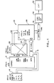
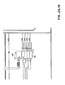
- the image data generation circuit 10 comprises a graphics system processor 12.
- the graphics system processor 12 is preferably a conventional graphics systems processor integrated circuit, for example, a Texas Instruments TMS34010 Graphics System Processor (GSP).
- GSP Graphics System Processor
- the operation and programming instructions for this processor are described in "Texas Instruments TMS34010 User's Guide” published in 1988 by Texas Instruments.
- the graphics system processor 12 is programmed in a conventional manner to read raw data from a display list memory 14 on an I/O data bus 16 which interconnects the graphics system processor and the display list memory. At least a portion of the raw data is stored in the display list memory 14 in X,Y coordinate form.
- the first cycle of the graphics system processor 12 after reading the raw data in X,Y coordinate form is to transpose this raw data to Y,X coordinate form.
- the graphics system processor 12 then commences a line drawing operation which translates the raw data to a pictorial representation in the form of image data.
- the graphics system processor 12 reads one X,Y coordinate from the display list memory 14 and then reads the adjacent X,Y coordinate from the display list memory. The graphics system processor 12 then transposes the X and Y coordinates for these points. Next, the graphics system processor 12 determines the horizontal separation between the points.
- the vertical spacing is determined. If the vertical spacing is greater than the horizontal separation, i.e., the slope is greater than 45 degrees, then the line is broken into a set of vertical line segments offset horizontally from one another by one pixel. Next, if the cumulative offset between X coordinates is one, the line is broken into two segments of equal length, ignoring round-off. If, on the other hand, the cumulative offset is two or more, the number of segments is computed to be Delta X plus where Delta X equals the number of pixels separating the adjacent X coordinates.
- each vertical segment is then determined by computing the vertical spacing so as to determine the number of pixels between the Y coordinates of the adjacent points, inclusive of the end points, and dividing the result by Delta X, ignoring round-off.
- the first and last segments are preferably half the length (number of pixels) of the remaining segments. This last feature is so that the broken line connects well with the preceding and/or subsequent lines, if any. Interestingly, this produces the same result as Bresenham's line-drawing algorithm, but the graphics system processor 12 performs the modified line drawing procedure in accordance with the invention considerably faster, on the average of ten times faster using the TMS34010 GSP.
- the graphics system processor 12 executes a routine which examines the now horizontally oriented line that has been broken into a series of individual horizontal line segments. Since these line segments are horizontal, and not just horizontally oriented, it is now possible to use the fill rectangle command (“FILL") of the graphics system processor 12, which is very fast at drawing horizontal lines.
- FILL fill rectangle command
- the image data generated by the graphics system processor 12 appears on the I/0 data bus 16 in Y,X coordinate form with the Y,X coordinate address information appearing on output address lines 18 and 20 of the graphics system processor.
- the graphics system processor 12 converts the X,Y pixel location into a video memory address, it uses the X value as the least significant portion of the video memory address and the Y value as the most significant portion of the video memory address. But since the X and Y values have been exchanged, the video memory address that is generated will have the least significant portion generated from the Y value, and the most significant portion generated from the X value.
- the Y coordinate address line 18 and X coordinate address line 20 are therefore connected to an address translator circuit 22 included in the image data generation circuit 10.
- the address translator circuit 22 converts the address information on the Y and X coordinate address lines 18 and 20 to X and Y coordinate information on address lines 24 and 26, respectively.
- the address translator circuit 22 reverses it again. The result is that the Y-half (low order bits now) determine the row address in the video memory 28, and the X-half of the address (higher order bits now) determine the column address in the video memory.
- the X and Y coordinate address lines 24 and 26 are connected to the video memory 28 which also receives image data on the data I/0 bus 16.
- the video memory 28 stores image data in memory locations identified by the address information on the X and Y coordinate address lines 24 and 26 to write the image data into the appropriate memory locations for generating a raster display.
- the video memory 28 preferably comprises 16 VRAMs, arranged as four banks of four.
- the video memory 28 can comprise conventional 256K-bit video memories arranged as 64K x 4 VRAMs available from any one of a number of integrated circuit manufacturers.
- the video memory 28 also comprises a video memory shift register 28A into which image data for drawing each individual row of the raster display is sequentially written and subsequently fed on a video data bus 32 to a CRT 30 to modulate the electron beam.
- the CRT 30 can be a Sony Part Number CHM-7501-00 color monitor.
- the graphics system processor 12 accesses the video memory 28 in groups of either vertically adjacent memory cells or horizontally adjacent memory cells.
- the video memory 28 is accessed vertically, resulting in the writing of four vertically adjacent pixels a memory cycle.
- the video memory shift register 28A is accessed horizontally, shifting out four horizontally adjacent pixels per shift cycle to the CRT 30. The effect of this dual access is that it allows faster writing of vertical lines, yet it still allows conventional transfers of pixels to the CRT 30 for screen update or refresh.
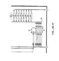
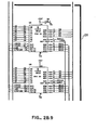
- Fig. 2 shows a detailed implementation of the image data generation circuit 10 shown in Fig. 1.
- the correspondence between the elements of the block diagram in Fig. 1 and the corresponding implementation shown in Fig. 2 is indicated by labeled boxes in Figs. 2A and 2B.
- measurement data is preferably entered through the graphics system processor 12 to the display list memory 14 shown in Fig. 2B, rather than directly to the display list memory.
- the graphics system processor 12 serves as a slave processor, and this operation does not form any part of the image data generation method in accordance with the invention.
- the high address information (X coordinate information) on address lines 20 appears at pins LAD 2 through LAD 11.
- the low address (Y coordinate information) appears on pins LAD 0 through LAD 9.
- Image data appears on pins LAD 0 through LAD 15. This occurs during three sequential output periods of the graphics system processor 12.
- circuitry which performs the video memory interface is shown on the right half of Fig 2A.
- the VRAMs of the video memory 28 are shown on the left half of Fig. 2B.
- the hardware is all standard off-the-shelf components. The component types are indicated in Figs. 2A and 2B.
- the address translator circuit 22 is preferably implemented by two PALs U49 and U50. This logic controls accesses to the video memory 28, choosing the proper VRAMs for a given memory cycle.
- This hardware latches the row address from the graphics system processor 12, using LRAS. Next, it sends the column address from the graphics system processor 12 to the VRAMs of the video memory 28, followed immediately by a LRAS signal. (This LRAS signal will come from the LCAS signal of the graphics system processor 12.) Thus, the VRAMs of the video memory 28 will use the column address as their row address.
- the hardware waits 24 nS, determined using the LCLK1 and LCLK2 outputs from the graphics system processor 12.
- the address information which appears on the address lines 24 and 26 is preferably multiplexed to the video memory 28 (Fig. 2B) on lines AO through A7.
- a DMUX U46 and latch U47 shown below block 22 in Fig. 2A, interconnect the graphics system processor 12 and the video memory 28 (Fig. 2B) to control loading and shifting of the video memory shift register 28A whose outputs appear on lines SDO through SD15 from the video memory, which form the video data bus 32.
- the four D flip-flops U30A, U30B, U41A, and U41B shown below the block 34 in Fig. 2B, provide the required timing on a shift control bus 38B that controls the shifting of image data from the shift register 28A.
- the X-half of an X,Y register constitutes the lowest order bits of the video memory address
- the Y-half of the X,Y register constitutes the higher order bits.
- the X and Y halves of the X,Y register need to be arranged exactly the opposite. The solution is to reverse the X and Y positions in the registers of the graphics system processor 12, and then to reverse the row and column address lines going to the VRAMs of the video memory 28.
- the X and Y pixel coordinates are reversed in software, defining the lower half of each X,Y register as the Y half and the upper half as the X half.
- Transposing the X and Y addresses requires additional hardware to reverse the row and column addresses supplied by the graphics system processor 12 before they are presented to the VRAMs of the video memory 28.
- the address translator circuit 22 reverses the X and Y pixel address coordinates during drawing cycles of the graphics system processor 12, but maintains standard addressing for screen update or refresh and memory update or refresh.
- the pixels end up being stored in VRAM with their X and Y values oriented in a standard manner. It is now possible to shift these pixels out to the CRT 30 in a standard fashion.
- the image data generation circuit 10 also preferably includes a pixel processing circuit 34 connected between the video memory shift register 28A and the CRT 30.
- the pixel processing circuit 34 replicates pixels based on the image data that appears on the video data bus 32 to double the width of the trace displayed on the CRT 30.
- Pixel stretching is a method of doubling pixel positionability in the horizontal direction, while not actually doubling the resolution requirements of the CRT 30.
- To implement pixel stretching the horizontal resolution of the raster display is doubled, resulting in much smoother appearing, near-vertical lines.
- a resolution of 512 x 400 (identical to a Series 300 Bobcat computer with medium resolution graphics and 35741 display) is initially chosen. In accordance with pixel stretching, the resolution is doubled to 1024 x 400. In spite of the doubled horizontal resolution and video rate, the same 512 x 400 CRT can be used. The reason is that the video input signal to the CRT is still composed of standard 1/512 width pixels (1/1024 * 2). The only difference is that the pixels are sometimes offset half a pixel width, due to 1/1024 positionability. Note that since each pixel is still 1/512th of a line wide, and not 1/1024th, the bandwidth requirements of the CRT are not increased.
- Table III illustrates an example of how a vertically oriented line would appear using various display techniques. Each "X" represents 1/1024th of the screen width.
- the screen of a color RGB monitor can be thought of as a continuous field of RGB phosphor and not discrete colored phosphor trios.
- This conceptualization is valid because the electron beam which strikes the phosphor has a Gaussian distribution about its center. This distribution causes approximately 2.67 phosphor trios on the face of the CRT to glow. (A portion of this wide distribution is caused by the inability to turn the electron beam on or off instantaneously.)
- the brain quantifies the spot, making it appear to be emanating from a single point, not 2.67 individual phosphor trios.
- the exact point of electron beam landing be it centered on a trio or in between two trios, has little effect on the resultant image.
- Pixel stretching is preferably implemented in hardware.
- the pixel processing circuit 34 comprises two multiplexers U15 and U16 for a 16-to-8-bit data reduction connected to a latch U29 and a PAL U14. Each adjacent pair of pixels enters the pixel stretching PAL U14.
- This PAL uses the following stretching algorithm. IF the current pixel is a background color (0000), THEN output the previous value of the pixel (stretch it). IF the current pixel is NOT a background color (0001...1111), THEN output the current pixel (don't stretch the previous pixel).
- An example of pixel stretching follows.
- a video palette U1 is connected to the outputs of the pixel processing circuit 34 for converting the digital image data to analog signals which are input to the CRT 30.
- the detailed circuit of CRT 30 is omitted from Fig. 2, since it forms no part of this invention.
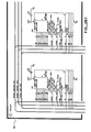
- the graphics system processor 12 initially reads X,Y values from the display list memory 14, as indicated by the numeral 100. In accordance with the method of the invention, the graphics system processor 12 next reverses X and Y values to Y and X values, as indicated by the numeral 102. Then, the graphics system processor 12 examines the direction of the reversed line joining adjacent Y,X values, as indicated by the numeral 104.
- the graphics system processor 12 breaks the reversed line into a series of horizontal line segments, as indicated by the numeral 106. Then, the graphics system processor 12 draws line segments using the "FILL" command, as indicated by the numeral 108.
- the address translator circuit 22 After the graphics system processor 12 executes the "FILL" command to draw line segments in groups of four horizontally adjacent pixels, as indicated by the numeral 110, the address translator circuit 22 reverses the upper and lower halves of the address bus, essentially reversing X and Y values, as indicated by the numeral 112. This selects the video memory 28 to allow writing of pixel data into four vertically adjacent memory cells (locations), as indicated by the numeral 114. The pixel data is thus written into the video memory 28 in conventional format, as indicated by the numeral 116.
- the graphics system processor 12 draws a line using a conventional "LINE" command, as indicated by the numeral 118. Accordingly, the graphics system processor 12 executes the "LINE" command to write one pixel at a time into the video memory 28, as indicated by the numeral 120. This is relatively slow, due to a read/modify/write process described in more detail below, and added computation.
- the address translator circuit 22 reverses the upper and lower halves of the address bus, essentially reversing X and Y values, as indicated by the numeral 122.
- the graphics system processor 12 next reads four vertically adjacent pixels from the video memory 28, three are masked, and one is modified, and then the resultant pixel data is written into four vertically adjacent memory cells in the video memory, as indicated by the numeral 124. The pixel data is thus written into the video memory 28 in conventional format, as indicated by the numeral 116.
- the pixel data is read into the video memory shift register 28A and shifted out as indicated by the numeral 126.
- pixels are stretched, as indicated by the numeral 128.
- the image is displayed by the CRT 30, as indicated by the numeral 130.
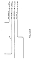
- the conventional line drawing process of the graphics system processor 12 is improved to smoothly and consistently track vertical transitions in traces. This is particularly useful in displaying measurement data traces of instruments, such as network analyzers. An exemplary trace appears in Fig. 4.
- Table V below compares the drawing speed of the TMS34010 GSP as it was designed to be used versus being incorporated into the image data generation circuit 10 when drawing vertical lines.
Abstract
Description
- This invention relates to creation of images and, more particularly, to generation of images on raster displays. These images can consist of textual and/or graphical information. Specifically, the invention is directed to a method and apparatus for digitally processing image data, which increase the speed or rate of generation of corresponding images on a raster display.
- One type of raster display is a cathode ray tube (CRT) on which images are displayed by a technique known as raster scanning. Raster scanning involves driving a deflection control circuit which directs an electron beam modulated by image information onto discrete areas of luminescent material on a display screen. The image information determines whether or not each discrete luminescent area is illuminated. Typically, raster scanning involves sweeping the electron beam from the upper left hand corner of the screen horizontally across the screen to the right to selectively illuminate a horizontal row of discrete luminescent areas and repeating the process for each row of the screen from top to bottom, selectively illuminating each discrete luminescent area in accordance with the corresponding image information which modulates the electron beam.
- The electron beam can be modulated in various ways depending on the manner in which the CRT is being used. One example is a television in which image information is transmitted through the atmosphere and detected by a television receiver which decodes the received image information and modulates the electron beam to display images on a screen. The deflection control circuit sweeps the electron beam to generate images on a television screen as many as 60 times a second.
- CRTs are also used as displays for other purposes. One such use is in computer terminals. Here, images are displayed by sweeping the electron beam in the same way as in a television. Unlike television, however, the image information is not generally transmitted through the atmosphere, but rather is input to the computer at a local or remote location and stored in a screen memory. A display control processor feeds the stored image data in the screen memory to the CRT for modulating the electron beam to generate an image corresponding to the stored image data.
- Another use of a CRT is in electronic instrumentation, such as an oscilloscope, spectrum analyzer, or network analyzer. These instruments measure characteristics of received signals transmitted through the atmosphere or responses of electronic devices connected to them. Typically, the measured information is processed and stored in a screen memory, similar to the way in which image data is stored in the screen memory for display on computer terminals.
- Unlike computer terminals in which data is entered and displayed at relatively low rates or speeds, instruments make measurements at significantly higher speeds. For example, data can be entered in computer terminals by a keyboard at typing speed, say at an average of 80 characters a minute, whereas sophisticated instruments make measurements at a rate of between 300 to 3,600 times a minute.
- In most instruments with CRTs, standard off-the-shelf graphics system processors are used to update the display, due to their relatively low cost (compared to custom graphics system processors or dedicated graphics engines). The resultant update rate is typically two to five times a second during normal measurement operation. Examples of such instruments include the Hewlett-Packard Company HP 4195A Network/Spectrum Analyzer, HP 54110 Color Digitizing Oscilloscope, and HP 70000 Modular Measurement System, as well as the Wiltron Company 360, Wiltron 561, and wiltron 6409 network analyzers.
- Achieving a fast display update rate is very important in many instrument applications. If the display cannot be updated as fast as measurements are made, the data collection process must be slowed down, or else the user of the instrument will not see the data that has been collected. The measurement traces will be updated sluggishly, making the instrument less responsive to the user. In addition, if the display is not updated quickly, the instrument will not have a "real-time" feel; that is, the images will dance in steps to the final displayed values rather than appear to move smoothly and instantaneously to those final values as the display is updated with new measurement data that has been collected. A display update rate of at least 10 to 20 updates a second (10 to 20 Hz) is needed in order to achieve a "real-time" feel.
- One disadvantage of raster displays used in instruments is that pixels on the display screen must be written by the graphics system processor into a region of screen memory. The process of writing image data corresponding to a single line into the screen memory can require the graphics system processor to access hundreds of screen memory locations, consuming a significant amount of time.
- In fast instruments, which make measurements at 3,000 or so times a minute (as fast as 60 Hz), changes in the measured data are not faithfully displayed on the CRT quickly because of limitations of the graphics system processor which is not able to quickly fill video memory at a rate that can be accommodated by the 60 Hz maximum update capability of the deflection control circuit of conventional CRTs. It is desirable that the rate or speed with which image data can be processed can be better matched to the display update capability of the deflection control circuit of the raster display so that changes in images can be more quickly updated on the raster display and perceived by the user.
- One embodiment of the invention increases the speed with which image data is written into a screen memory. Accordingly, the image data is stored in a manner which enables updated image data to be accessed and displayed more quickly on a raster display, such as a CRT, by the use of a conventional deflection control circuit and raster scanning technique. For example, the invention results in an eight-fold increase in the speed of updating the display of traces of measurement data in a network analyzer. This enables new measurement data to be more rapidly displayed to the user without the data trace appearing to dance on the screen.
- In accordance with one embodiment of the method and apparatus in accordance with the invention, a graphics system processor receives information which is to be displayed. At least a portion of this information is in the form of X,Y coordinate data. The graphics system processor transposes each received set of X and Y coordinates so that X,Y becomes Y,X. The graphics system processor then processes adjacent pairs of transposed coordinates to generate a line segment or segments by using the first set of transposed coordinates as the starting point and the second set of transposed coordinates as the end point. Next, the graphics system processor can compute a best-fit set of points between the starting and end points to interconnect them using a conventional technique, such as Bresenham's line-drawing algorithm. Preferably, the method in accordance with one embodiment of the invention optimizes the line segment drawing process in the graphics system processor.
- The graphics system processor is connected to a conventional screen or video memory which stores the image or video data produced by the graphics system processor. In order to write the image data into the video memory so that the image data is properly fed to modulate the electron beam of the CRT, an address translator circuit interfaces the graphics system processor to the video memory. The address translator circuit writes the image data in banks of vertically oriented image data, as compared to horizontally oriented banks of image data, so that image data is stored in the video memory in a conventional format for updating the display on the CRT. The address translator circuit writes into the video memory by reversing the address select lines to the video memory so that the image data is correctly stored for later access.
- By first transposing the coordinates with the graphics system processor and digitally processing in a conventional horizontal mode, changes in vertical distances between adjacent points of information are more quickly written into the video memory and hence more quickly reflected on the screen of the CRT as the electron beam is modulated in the conventional way. In other words, limitations on the speed of operation of the graphics system processor are removed by allowing the graphics system processor to operate in a pseudo-horizontal mode without affecting the appropriate image data storage needed to generate the CRT display. Accordingly, the graphics system processor is able to process image data characterized by vertical excursions as fast as conventional processing of image data, such as horizontal line drawing. The address translator then reconverts the image data to the appropriate form for conventional storage in the screen memory so that a conventional CRT can be used. Also, a pulse stretching circuit is preferably provided to replicate an adjacent pixel for each pixel of each line segment to provide a smooth, high resolution trace.
- The above and other features of the invention and the concomitant advantages will be better understood and appreciated by persons skilled in the art in view of the detailed description given below in conjunction with the accompanying drawings. In the drawings:
- Fig. 1 is a block diagram of one embodiment of an image data generation circuit in accordance with the invention;
- Fig. 2, comprising Figs. 2A and 2B, is a detailed schematic drawing of one implementation of the image data generation circuit shown in Fig. 1;
- Fig. 3 is a flow chart of one embodiment of the method in accordance with the invention for speeding generation of raster displays; and
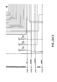
- Fig. 4 illustrates an example of a trace generated from measurement data in accordance with one embodiment of the invention.
- The following additional background information is intended to facilitate an understanding of the invention. Typically, the graphics system processor and its associated video memory are optimized to operate with image data being written into horizontally adjacent memory cells in the video memory. This constraint is imposed by a conventional deflection control circuit in a CRT, which raster scans horizontally, and the required interconnection of the video memory output shift register to the deflection control circuit for modulating the electron beam of the CRT. This constraint slows the speed of the graphics system processor in processing measurement data for display, since measurement data is typified by vertical excursions as opposed to horizontal ones. Therefore, more time is required to update the video memory when sequential measurements vary.
- Considered in more detail, in many instrument applications, the data display is a graph, with the controlled variable drawn along the X-axis, and the independent variable drawn along the Y-axis. (See, for example, Fig. 4.) Such graphs tend to exhibit a more rapid data variation in the Y direction than in the X direction. As a result, the graph is predominantly composed of vertically oriented lines and contains far fewer horizontally oriented lines.
- There are various significant disadvantages of off-the-shelf graphics systems processors. Unfortunately, presently available off-the-shelf graphics system processors are typically designed in a way that optimizes their drawing speed in the horizontal direction. This results in much lower performance when drawing in the vertical direction. Generally, horizontal lines can be drawn two to 16 times faster than vertical lines. In order to achieve a rapid display update rate, the graphics system processor must be able to draw vertical lines very quickly.
- For example, one conventional graphics system processor has a 16-bit data bus, allowing it to write four 4-bit pixels to the video memory in one cycle. The graphics system processor is designed such that the four pixels it writes during a memory cycle are horizontally adjacent. Hence, the standard technique of interfacing the graphics system processor to the video memory is to have it access four 64K x 4 video dynamic random access memories (VRAMs) in parallel. The result is that the adjacent pixels on a horizontal raster scan line are interleaved among the four VRAMs. When the pixels are to be shifted out of the VRAMs to the CRT, the four banks are all shifted simultaneously, and the interleaved pixels are multiplexed onto a single video bus.
- Typically, the number of bits per pixel, n, is 1, 2, or 4. If, for example, 16 colors are desired on a CRT, four bits per pixel are needed to specify one of the colors. Since the graphics system processor accesses 16 bits of memory per cycle, it is able to write 16, 8, or 4 pixels to memory per cycle, respectively. Thus, m, the number of graphics system processor data outputs (16-bit data bus) divided by the number of bits per pixel, n, is 4 for a 16-color CRT. The pixels that are written together in a single memory cycle are pixels that are horizontally adjacent in video memory rather than vertically adjacent for the following reason.
- The video memory is configured in such a way that the horizontally adjacent memory cells (which each contain a pixel) have adjacent addresses. That is, incrementing the video memory address by one results in the selection of the pixel immediately to the right of the current pixel.
- Accordingly, graphics system processors are typically designed to work with standard video memories. This requires that they be architected in such a way that they convert the X,Y position of a pixel into a video memory address in which Y selects the most significant portion of the address and X selects the least significant portion of the address. Since the graphics system processor accesses several horizontally adjacent pixels in a single memory cycle, it is able to generate horizontal lines significantly faster than vertical lines.
- The method and apparatus in accordance with the invention alter the graphics system processor to operate as though it is drawing horizontal lines, when it is actually drawing vertical lines. This is achieved by exchanging the X and Y coordinates of each line segment endpoint and computing vertical line segments in a pseudo-horizontal mode. Then, the X and Y halves of the memory address are exchanged by means of an address translator circuit so that image data is written into the video memory in the appropriate format for modulating the electron beam.
- A preferred embodiment of the image data generation circuit in accordance with the invention, generally indicated by the numeral 10, is shown in Fig. 1. The image
data generation circuit 10 comprises agraphics system processor 12. Thegraphics system processor 12 is preferably a conventional graphics systems processor integrated circuit, for example, a Texas Instruments TMS34010 Graphics System Processor (GSP). The operation and programming instructions for this processor are described in "Texas Instruments TMS34010 User's Guide" published in 1988 by Texas Instruments. - The
graphics system processor 12 is programmed in a conventional manner to read raw data from adisplay list memory 14 on an I/O data bus 16 which interconnects the graphics system processor and the display list memory. At least a portion of the raw data is stored in thedisplay list memory 14 in X,Y coordinate form. - In accordance with the invention, the first cycle of the
graphics system processor 12 after reading the raw data in X,Y coordinate form is to transpose this raw data to Y,X coordinate form. Thegraphics system processor 12 then commences a line drawing operation which translates the raw data to a pictorial representation in the form of image data. - Considered in more detail, the
graphics system processor 12 reads one X,Y coordinate from thedisplay list memory 14 and then reads the adjacent X,Y coordinate from the display list memory. Thegraphics system processor 12 then transposes the X and Y coordinates for these points. Next, thegraphics system processor 12 determines the horizontal separation between the points. - Preferably, if the horizontal spacing is less than a predetermined distance, for example, less than two pixels, the vertical spacing is determined. If the vertical spacing is greater than the horizontal separation, i.e., the slope is greater than 45 degrees, then the line is broken into a set of vertical line segments offset horizontally from one another by one pixel. Next, if the cumulative offset between X coordinates is one, the line is broken into two segments of equal length, ignoring round-off. If, on the other hand, the cumulative offset is two or more, the number of segments is computed to be Delta X plus where Delta X equals the number of pixels separating the adjacent X coordinates. The length of each vertical segment is then determined by computing the vertical spacing so as to determine the number of pixels between the Y coordinates of the adjacent points, inclusive of the end points, and dividing the result by Delta X, ignoring round-off. Finally, the first and last segments are preferably half the length (number of pixels) of the remaining segments. This last feature is so that the broken line connects well with the preceding and/or subsequent lines, if any. Interestingly, this produces the same result as Bresenham's line-drawing algorithm, but the
graphics system processor 12 performs the modified line drawing procedure in accordance with the invention considerably faster, on the average of ten times faster using the TMS34010 GSP. - To perform the actual line drawing, the
graphics system processor 12 executes a routine which examines the now horizontally oriented line that has been broken into a series of individual horizontal line segments. Since these line segments are horizontal, and not just horizontally oriented, it is now possible to use the fill rectangle command ("FILL") of thegraphics system processor 12, which is very fast at drawing horizontal lines. - As the
graphics system processor 12 generates the horizontal line segments of each line, it takes each group of m horizontally adjacent pixels and attempts to write them to video memory in a single cycle. (m can be calculated as the width of the data bus of thegraphics system processor 12 divided by the number of bits per pixel, and, typically, m = 4, 8, or 16. In an exemplary application of the invention in which 16 colors are available, m = 16 / 4 = 4.) This technique of writing multiple horizontally adjacent pixels in each memory cycle is what makes horizontal line drawing fast. Table I below is a listing of the source code for a Texas Instruments TMS34010 GSP, which performs this line drawing operation. -


- The image data generated by the
graphics system processor 12 appears on the I/0data bus 16 in Y,X coordinate form with the Y,X coordinate address information appearing onoutput address lines graphics system processor 12 converts the X,Y pixel location into a video memory address, it uses the X value as the least significant portion of the video memory address and the Y value as the most significant portion of the video memory address. But since the X and Y values have been exchanged, the video memory address that is generated will have the least significant portion generated from the Y value, and the most significant portion generated from the X value. - In order to write the pixels into the proper, conventional locations in a
video memory 28, it is now necessary to exchange the upper and lower portions of the address bus before presenting the address to the video memory. The Y coordinateaddress line 18 and X coordinateaddress line 20 are therefore connected to anaddress translator circuit 22 included in the imagedata generation circuit 10. Theaddress translator circuit 22 converts the address information on the Y and X coordinateaddress lines address lines graphics system processor 12 outputs the video memory address, theaddress translator circuit 22 reverses it again. The result is that the Y-half (low order bits now) determine the row address in thevideo memory 28, and the X-half of the address (higher order bits now) determine the column address in the video memory. - The X and Y coordinate
address lines video memory 28 which also receives image data on the data I/0bus 16. Thevideo memory 28 stores image data in memory locations identified by the address information on the X and Y coordinateaddress lines - In accordance with the invention, the
video memory 28 preferably comprises 16 VRAMs, arranged as four banks of four. For example, thevideo memory 28 can comprise conventional 256K-bit video memories arranged as 64K x 4 VRAMs available from any one of a number of integrated circuit manufacturers. - The
video memory 28 also comprises a videomemory shift register 28A into which image data for drawing each individual row of the raster display is sequentially written and subsequently fed on avideo data bus 32 to aCRT 30 to modulate the electron beam. For example, theCRT 30 can be a Sony Part Number CHM-7501-00 color monitor. - Accordingly, the
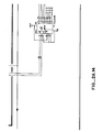
graphics system processor 12 accesses thevideo memory 28 in groups of either vertically adjacent memory cells or horizontally adjacent memory cells. During drawing, thevideo memory 28 is accessed vertically, resulting in the writing of four vertically adjacent pixels a memory cycle. During screen update or refresh, the videomemory shift register 28A is accessed horizontally, shifting out four horizontally adjacent pixels per shift cycle to theCRT 30. The effect of this dual access is that it allows faster writing of vertical lines, yet it still allows conventional transfers of pixels to theCRT 30 for screen update or refresh. - Fig. 2, comprising Figs. 2A and 2B, shows a detailed implementation of the image
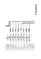
data generation circuit 10 shown in Fig. 1. The correspondence between the elements of the block diagram in Fig. 1 and the corresponding implementation shown in Fig. 2 is indicated by labeled boxes in Figs. 2A and 2B. - As shown in Fig. 2A, measurement data is preferably entered through the
graphics system processor 12 to thedisplay list memory 14 shown in Fig. 2B, rather than directly to the display list memory. During this operation, thegraphics system processor 12 serves as a slave processor, and this operation does not form any part of the image data generation method in accordance with the invention. - Referring to Fig. 2A, the high address information (X coordinate information) on
address lines 20 appears atpins LAD 2 throughLAD 11. The low address (Y coordinate information) appears onpins LAD 0 throughLAD 9. Image data appears onpins LAD 0 throughLAD 15. This occurs during three sequential output periods of thegraphics system processor 12. - Generally, the circuitry which performs the video memory interface is shown on the right half of Fig 2A. The VRAMs of the
video memory 28 are shown on the left half of Fig. 2B. The hardware is all standard off-the-shelf components. The component types are indicated in Figs. 2A and 2B. - The
address translator circuit 22 is preferably implemented by two PALs U49 and U50. This logic controls accesses to thevideo memory 28, choosing the proper VRAMs for a given memory cycle. This hardware latches the row address from thegraphics system processor 12, using LRAS. Next, it sends the column address from thegraphics system processor 12 to the VRAMs of thevideo memory 28, followed immediately by a LRAS signal. (This LRAS signal will come from the LCAS signal of thegraphics system processor 12.) Thus, the VRAMs of thevideo memory 28 will use the column address as their row address. Next, the hardware waits 24 nS, determined using the LCLK1 and LCLK2 outputs from thegraphics system processor 12. Finally, it sends the row address (latched in the first step above) to the VRAMs of thevideo memory 28 followed immediately by a LCAS signal. (This LCAS signal will come from the LCAS signal of thegraphics system processor 12, delayed 24 nS.) Thus, the VRAMs of thevideo memory 28 will use the row address from thegraphics system processor 12 as their column address. The equations for the logic implemented in the two PALs U49 and U50 which implement theaddress translator circuit 22 are shown in Table II below.


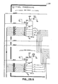
- As shown in the right hand portion of the
block 22 in Fig. 2A, the address information which appears on the address lines 24 and 26 is preferably multiplexed to the video memory 28 (Fig. 2B) on lines AO through A7. A DMUX U46 and latch U47, shown belowblock 22 in Fig. 2A, interconnect thegraphics system processor 12 and the video memory 28 (Fig. 2B) to control loading and shifting of the videomemory shift register 28A whose outputs appear on lines SDO through SD15 from the video memory, which form thevideo data bus 32. The four D flip-flops U30A, U30B, U41A, and U41B, shown below theblock 34 in Fig. 2B, provide the required timing on a shift control bus 38B that controls the shifting of image data from theshift register 28A. - In summary, in the
graphics system processor 12, the X-half of an X,Y register constitutes the lowest order bits of the video memory address, and the Y-half of the X,Y register constitutes the higher order bits. In order to draw vertical lines quickly, the X and Y halves of the X,Y register need to be arranged exactly the opposite. The solution is to reverse the X and Y positions in the registers of thegraphics system processor 12, and then to reverse the row and column address lines going to the VRAMs of thevideo memory 28. - Accordingly, the X and Y pixel coordinates are reversed in software, defining the lower half of each X,Y register as the Y half and the upper half as the X half. Transposing the X and Y addresses requires additional hardware to reverse the row and column addresses supplied by the
graphics system processor 12 before they are presented to the VRAMs of thevideo memory 28. Accordingly, theaddress translator circuit 22 reverses the X and Y pixel address coordinates during drawing cycles of thegraphics system processor 12, but maintains standard addressing for screen update or refresh and memory update or refresh. - Doing so, the pixels end up being stored in VRAM with their X and Y values oriented in a standard manner. It is now possible to shift these pixels out to the
CRT 30 in a standard fashion. - As shown in Fig. 1, the image
data generation circuit 10 also preferably includes apixel processing circuit 34 connected between the videomemory shift register 28A and theCRT 30. Thepixel processing circuit 34 replicates pixels based on the image data that appears on thevideo data bus 32 to double the width of the trace displayed on theCRT 30. - Pixel stretching is a method of doubling pixel positionability in the horizontal direction, while not actually doubling the resolution requirements of the
CRT 30. To implement pixel stretching, the horizontal resolution of the raster display is doubled, resulting in much smoother appearing, near-vertical lines. - In doubling the horizontal resolution alone, a problem occurs. Vertically oriented lines are now twice as thin as horizontal lines, and so they appear much dimmer. To compensate for this dimming, each pixel is stretched to twice its width in the horizontal direction. The result is vertically oriented lines of proper brightness and with improved smoothness.
- A resolution of 512 x 400 (identical to a Series 300 Bobcat computer with medium resolution graphics and 35741 display) is initially chosen. In accordance with pixel stretching, the resolution is doubled to 1024 x 400. In spite of the doubled horizontal resolution and video rate, the same 512 x 400 CRT can be used. The reason is that the video input signal to the CRT is still composed of standard 1/512 width pixels (1/1024 * 2). The only difference is that the pixels are sometimes offset half a pixel width, due to 1/1024 positionability. Note that since each pixel is still 1/512th of a line wide, and not 1/1024th, the bandwidth requirements of the CRT are not increased.
- Table III below illustrates an example of how a vertically oriented line would appear using various display techniques. Each "X" represents 1/1024th of the screen width.

- Since the CRT has a horizontal resolution of only 512 pixels, the question arises whether or not 1024 pixels can be mapped onto it. Won't some pixels land between the colored phosphors?
- The answer is that the screen of a color RGB monitor can be thought of as a continuous field of RGB phosphor and not discrete colored phosphor trios. This conceptualization is valid because the electron beam which strikes the phosphor has a Gaussian distribution about its center. This distribution causes approximately 2.67 phosphor trios on the face of the CRT to glow. (A portion of this wide distribution is caused by the inability to turn the electron beam on or off instantaneously.) When viewed by the human eye, the brain quantifies the spot, making it appear to be emanating from a single point, not 2.67 individual phosphor trios. Thus, the exact point of electron beam landing, be it centered on a trio or in between two trios, has little effect on the resultant image.
- Pixel stretching is preferably implemented in hardware. As shown in Fig. 2B, the
pixel processing circuit 34 comprises two multiplexers U15 and U16 for a 16-to-8-bit data reduction connected to a latch U29 and a PAL U14. Each adjacent pair of pixels enters the pixel stretching PAL U14. This PAL uses the following stretching algorithm. IF the current pixel is a background color (0000), THEN output the previous value of the pixel (stretch it). IF the current pixel is NOT a background color (0001...1111), THEN output the current pixel (don't stretch the previous pixel). An example of pixel stretching follows. - input: ......R...G.B....... (R,G,B = colors)
- result: ......RR..GGBB...... (. = background)
- input: .......RGB..........
- result: .......RGBB.........
- Note that the red and green pixels cannot be stretched to their full width, but they are still displayed at their unstretched width (limited somewhat by CRT bandwidth). On a 512-pixel wide screen, however, only two pixels could have been displayed in the same case, due to its lower resolution. Hence, pixel stretching is still advantageous. The PAL equations for the PAL U14 appear in Table IV below.


- As shown in the right hand portion of Fig. 2B, a video palette U1 is connected to the outputs of the
pixel processing circuit 34 for converting the digital image data to analog signals which are input to theCRT 30. For the sake of simplification, the detailed circuit ofCRT 30 is omitted from Fig. 2, since it forms no part of this invention. - Operation of the image
data generation circuit 10 is summarized in the flow chart shown in Fig. 3. As shown in Fig. 3, thegraphics system processor 12 initially reads X,Y values from thedisplay list memory 14, as indicated by the numeral 100. In accordance with the method of the invention, thegraphics system processor 12 next reverses X and Y values to Y and X values, as indicated by the numeral 102. Then, thegraphics system processor 12 examines the direction of the reversed line joining adjacent Y,X values, as indicated by the numeral 104. - On the one hand, if the slope of the reversed line is nearly horizontal, as indicated by the numeral 105, the
graphics system processor 12 breaks the reversed line into a series of horizontal line segments, as indicated by the numeral 106. Then, thegraphics system processor 12 draws line segments using the "FILL" command, as indicated by the numeral 108. - After the
graphics system processor 12 executes the "FILL" command to draw line segments in groups of four horizontally adjacent pixels, as indicated by the numeral 110, theaddress translator circuit 22 reverses the upper and lower halves of the address bus, essentially reversing X and Y values, as indicated by the numeral 112. This selects thevideo memory 28 to allow writing of pixel data into four vertically adjacent memory cells (locations), as indicated by the numeral 114. The pixel data is thus written into thevideo memory 28 in conventional format, as indicated by the numeral 116. - On the other hand, if the slope of the reversed line is not nearly horizontal, as determined by the
step 105, thegraphics system processor 12 draws a line using a conventional "LINE" command, as indicated by the numeral 118. Accordingly, thegraphics system processor 12 executes the "LINE" command to write one pixel at a time into thevideo memory 28, as indicated by the numeral 120. This is relatively slow, due to a read/modify/write process described in more detail below, and added computation. - Then, the
address translator circuit 22 reverses the upper and lower halves of the address bus, essentially reversing X and Y values, as indicated by the numeral 122. In accordance with the read/modify/write process, thegraphics system processor 12 next reads four vertically adjacent pixels from thevideo memory 28, three are masked, and one is modified, and then the resultant pixel data is written into four vertically adjacent memory cells in the video memory, as indicated by the numeral 124. The pixel data is thus written into thevideo memory 28 in conventional format, as indicated by the numeral 116. - Next, the pixel data is read into the video
memory shift register 28A and shifted out as indicated by the numeral 126. Preferably, pixels are stretched, as indicated by the numeral 128. Finally, the image is displayed by theCRT 30, as indicated by the numeral 130. - In accordance with the invention, the conventional line drawing process of the
graphics system processor 12 is improved to smoothly and consistently track vertical transitions in traces. This is particularly useful in displaying measurement data traces of instruments, such as network analyzers. An exemplary trace appears in Fig. 4. - Table V below compares the drawing speed of the TMS34010 GSP as it was designed to be used versus being incorporated into the image
data generation circuit 10 when drawing vertical lines.
video memory 28 and a corresponding increase in the speed of updating theCRT 30. - The foregoing description is offered primarily for purposes of illustration. While a variety of embodiments of the image data generation method and apparatus in accordance with the invention has been disclosed, it will be readily apparent to those skilled in the art that numerous other modifications and variations not mentioned above can still be made without departing from the spirit and scope of the invention as claimed below.
It is possible for a group of non-background color pixels to be packed so closely together that some of them cannot be stretched. For example, let's suppose that there were three adjacent red, green, and blue pixels.
Claims (21)
Applications Claiming Priority (2)
| Application Number | Priority Date | Filing Date | Title |
|---|---|---|---|
| US278873 | 1988-12-01 | ||
| US07/278,873 US4992961A (en) | 1988-12-01 | 1988-12-01 | Method and apparatus for increasing image generation speed on raster displays |
Publications (3)
| Publication Number | Publication Date |
|---|---|
| EP0371231A2 true EP0371231A2 (en) | 1990-06-06 |
| EP0371231A3 EP0371231A3 (en) | 1991-06-19 |
| EP0371231B1 EP0371231B1 (en) | 1993-12-15 |
Family
ID=23066740
Family Applications (1)
| Application Number | Title | Priority Date | Filing Date |
|---|---|---|---|
| EP89118104A Expired - Lifetime EP0371231B1 (en) | 1988-12-01 | 1989-09-29 | Method and apparatus for increasing image generation speed on raster displays |
Country Status (4)
| Country | Link |
|---|---|
| US (1) | US4992961A (en) |
| EP (1) | EP0371231B1 (en) |
| JP (1) | JPH0333793A (en) |
| DE (1) | DE68911492T2 (en) |
Cited By (2)
| Publication number | Priority date | Publication date | Assignee | Title |
|---|---|---|---|---|
| EP0568078A1 (en) * | 1992-04-30 | 1993-11-03 | Toshiba America Information Systems, Inc. | External interface for a high performance graphics adapter allowing for graphics compatibility |
| US5404445A (en) * | 1991-10-31 | 1995-04-04 | Toshiba America Information Systems, Inc. | External interface for a high performance graphics adapter allowing for graphics compatibility |
Families Citing this family (13)
| Publication number | Priority date | Publication date | Assignee | Title |
|---|---|---|---|---|
| CA2043493C (en) * | 1990-10-05 | 1997-04-01 | Ricky C. Hetherington | Hierarchical integrated circuit cache memory |
| US5442462A (en) * | 1992-06-10 | 1995-08-15 | D.V.P. Technologies Ltd. | Apparatus and method for smoothing images |
| US5799111A (en) * | 1991-06-14 | 1998-08-25 | D.V.P. Technologies, Ltd. | Apparatus and methods for smoothing images |
| US5313577A (en) * | 1991-08-21 | 1994-05-17 | Digital Equipment Corporation | Translation of virtual addresses in a computer graphics system |
| JPH05210481A (en) * | 1991-09-18 | 1993-08-20 | Ncr Internatl Inc | Direct access type video bus |
| US5289575A (en) * | 1991-11-22 | 1994-02-22 | Nellcor Incorporated | Graphics coprocessor board with hardware scrolling window |
| EP0843299B1 (en) * | 1992-09-30 | 2000-04-12 | Hudson Soft Co., Ltd. | Image processing apparatus |
| US5504503A (en) * | 1993-12-03 | 1996-04-02 | Lsi Logic Corporation | High speed signal conversion method and device |
| US5867178A (en) * | 1995-05-08 | 1999-02-02 | Apple Computer, Inc. | Computer system for displaying video and graphic data with reduced memory bandwidth |
| US6234521B1 (en) | 1996-04-08 | 2001-05-22 | Daicel Chemical Industries, Ltd. | Airbag inflator and an airbag apparatus |
| US6052107A (en) * | 1997-06-18 | 2000-04-18 | Hewlett-Packard Company | Method and apparatus for displaying graticule window data on a computer screen |
| US8395630B2 (en) * | 2007-01-02 | 2013-03-12 | Samsung Electronics Co., Ltd. | Format conversion apparatus from band interleave format to band separate format |
| CN113849143A (en) * | 2021-09-28 | 2021-12-28 | 上海顺久电子科技有限公司 | Display method, display device, and storage medium |
Citations (2)
| Publication number | Priority date | Publication date | Assignee | Title |
|---|---|---|---|---|
| EP0149188A2 (en) * | 1983-12-20 | 1985-07-24 | Ascii Corporation | Display control system |
| EP0164880A2 (en) * | 1984-05-07 | 1985-12-18 | Advanced Micro Devices, Inc. | A circuit for modifying data in a display memory |
Family Cites Families (6)
| Publication number | Priority date | Publication date | Assignee | Title |
|---|---|---|---|---|
| US4475161A (en) * | 1980-04-11 | 1984-10-02 | Ampex Corporation | YIQ Computer graphics system |
| US4459677A (en) * | 1980-04-11 | 1984-07-10 | Ampex Corporation | VIQ Computer graphics system |
| US4631750A (en) * | 1980-04-11 | 1986-12-23 | Ampex Corporation | Method and system for spacially transforming images |
| ATE45258T1 (en) * | 1981-04-10 | 1989-08-15 | Ampex | DEVICE FOR SPATIAL TRANSFORMATION OF IMAGES. |
| JPS6067989A (en) * | 1983-09-26 | 1985-04-18 | 株式会社日立製作所 | Image display circuit |
| US4799173A (en) * | 1986-02-28 | 1989-01-17 | Digital Equipment Corporation | Transformation circuit to effect raster operations |
-
1988
- 1988-12-01 US US07/278,873 patent/US4992961A/en not_active Expired - Lifetime
-
1989
- 1989-09-29 DE DE89118104T patent/DE68911492T2/en not_active Expired - Fee Related
- 1989-09-29 EP EP89118104A patent/EP0371231B1/en not_active Expired - Lifetime
- 1989-12-01 JP JP1313117A patent/JPH0333793A/en active Pending
Patent Citations (2)
| Publication number | Priority date | Publication date | Assignee | Title |
|---|---|---|---|---|
| EP0149188A2 (en) * | 1983-12-20 | 1985-07-24 | Ascii Corporation | Display control system |
| EP0164880A2 (en) * | 1984-05-07 | 1985-12-18 | Advanced Micro Devices, Inc. | A circuit for modifying data in a display memory |
Non-Patent Citations (1)
| Title |
|---|
| IBM JOURNAL OF RESEARCH AND DEVELOPMENT, vol. 28, no. 4, July 1984, pages 393-398, Armonk, New York, US; D.L. OSTAPKO: "A mapping and memory chip hardware which provides symmetric reading/writing of horizontal and vertical lines" * |
Cited By (3)
| Publication number | Priority date | Publication date | Assignee | Title |
|---|---|---|---|---|
| US5404445A (en) * | 1991-10-31 | 1995-04-04 | Toshiba America Information Systems, Inc. | External interface for a high performance graphics adapter allowing for graphics compatibility |
| EP0568078A1 (en) * | 1992-04-30 | 1993-11-03 | Toshiba America Information Systems, Inc. | External interface for a high performance graphics adapter allowing for graphics compatibility |
| US5438663A (en) * | 1992-04-30 | 1995-08-01 | Toshiba America Information Systems | External interface for a high performance graphics adapter allowing for graphics compatibility |
Also Published As
| Publication number | Publication date |
|---|---|
| JPH0333793A (en) | 1991-02-14 |
| EP0371231B1 (en) | 1993-12-15 |
| EP0371231A3 (en) | 1991-06-19 |
| DE68911492D1 (en) | 1994-01-27 |
| US4992961A (en) | 1991-02-12 |
| DE68911492T2 (en) | 1994-04-21 |
Similar Documents
| Publication | Publication Date | Title |
|---|---|---|
| EP0371231B1 (en) | Method and apparatus for increasing image generation speed on raster displays | |
| US4673929A (en) | Circuit for processing digital image data in a high resolution raster display system | |
| US4823120A (en) | Enhanced video graphics controller | |
| US4490797A (en) | Method and apparatus for controlling the display of a computer generated raster graphic system | |
| US4342029A (en) | Color graphics display terminal | |
| EP0710377B1 (en) | A data display apparatus and method for displaying digital samples of signal data on a bit mapped display system | |
| EP0019045B1 (en) | Graphics display apparatus | |
| EP0012420A1 (en) | Methods of operating display devices and apparatus for performing the methods | |
| EP0071744A2 (en) | Method for operating a computing system to write text characters onto a graphics display | |
| EP0012793A2 (en) | Method of displaying graphic pictures by a raster display apparatus and apparatus for carrying out the method | |
| KR910001564B1 (en) | A computer display system for producing color text and graphics | |
| US5237650A (en) | Method and apparatus for spatial anti-aliased depth cueing | |
| JPH0695273B2 (en) | Display control device | |
| JPH04220695A (en) | Gamma correcting apparatus for picture- element data in computer graphic system | |
| KR930002862A (en) | Display device and its driving method | |
| WO1993004461A1 (en) | High speed ramdac with reconfigurable color palette | |
| US4833462A (en) | Raster-scanned cathode ray tube display with cross-hair cursor | |
| JPS6221195A (en) | Reading circuit for image memory | |
| CA1304847C (en) | Display data conversion | |
| EP0202426B1 (en) | Raster scan digital display system | |
| US5023602A (en) | Raster graphical display apparatus | |
| US4703322A (en) | Variable loadable character generator | |
| EP0413483B1 (en) | A display system | |
| US5706025A (en) | Smooth vertical motion via color palette manipulation | |
| US4719456A (en) | Video dot intensity balancer |
Legal Events
| Date | Code | Title | Description |
|---|---|---|---|
| PUAI | Public reference made under article 153(3) epc to a published international application that has entered the european phase |
Free format text: ORIGINAL CODE: 0009012 |
|
| AK | Designated contracting states |
Kind code of ref document: A2 Designated state(s): DE FR GB NL |
|
| PUAL | Search report despatched |
Free format text: ORIGINAL CODE: 0009013 |
|
| AK | Designated contracting states |
Kind code of ref document: A3 Designated state(s): DE FR GB NL |
|
| 17P | Request for examination filed |
Effective date: 19911130 |
|
| 17Q | First examination report despatched |
Effective date: 19920723 |
|
| GRAA | (expected) grant |
Free format text: ORIGINAL CODE: 0009210 |
|
| AK | Designated contracting states |
Kind code of ref document: B1 Designated state(s): DE FR GB NL |
|
| PG25 | Lapsed in a contracting state [announced via postgrant information from national office to epo] |
Ref country code: FR Effective date: 19931215 |
|
| REF | Corresponds to: |
Ref document number: 68911492 Country of ref document: DE Date of ref document: 19940127 |
|
| EN | Fr: translation not filed | ||
| PLBE | No opposition filed within time limit |
Free format text: ORIGINAL CODE: 0009261 |
|
| STAA | Information on the status of an ep patent application or granted ep patent |
Free format text: STATUS: NO OPPOSITION FILED WITHIN TIME LIMIT |
|
| 26N | No opposition filed | ||
| PGFP | Annual fee paid to national office [announced via postgrant information from national office to epo] |
Ref country code: NL Payment date: 19980825 Year of fee payment: 10 |
|
| PGFP | Annual fee paid to national office [announced via postgrant information from national office to epo] |
Ref country code: GB Payment date: 19980826 Year of fee payment: 10 Ref country code: DE Payment date: 19980826 Year of fee payment: 10 |
|
| PG25 | Lapsed in a contracting state [announced via postgrant information from national office to epo] |
Ref country code: GB Free format text: LAPSE BECAUSE OF NON-PAYMENT OF DUE FEES Effective date: 19990929 |
|
| PG25 | Lapsed in a contracting state [announced via postgrant information from national office to epo] |
Ref country code: NL Free format text: LAPSE BECAUSE OF NON-PAYMENT OF DUE FEES Effective date: 20000401 |
|
| GBPC | Gb: european patent ceased through non-payment of renewal fee |
Effective date: 19990929 |
|
| NLV4 | Nl: lapsed or anulled due to non-payment of the annual fee |
Effective date: 20000401 |
|
| PG25 | Lapsed in a contracting state [announced via postgrant information from national office to epo] |
Ref country code: DE Free format text: LAPSE BECAUSE OF NON-PAYMENT OF DUE FEES Effective date: 20000701 |