EP0317827A2 - Computer system with logical monitoring for secure processing of system support signals - Google Patents
Computer system with logical monitoring for secure processing of system support signals Download PDFInfo
- Publication number
- EP0317827A2 EP0317827A2 EP88118676A EP88118676A EP0317827A2 EP 0317827 A2 EP0317827 A2 EP 0317827A2 EP 88118676 A EP88118676 A EP 88118676A EP 88118676 A EP88118676 A EP 88118676A EP 0317827 A2 EP0317827 A2 EP 0317827A2
- Authority
- EP
- European Patent Office
- Prior art keywords
- redundant
- arrangement
- power supply
- computer system
- computer
- Prior art date
- Legal status (The legal status is an assumption and is not a legal conclusion. Google has not performed a legal analysis and makes no representation as to the accuracy of the status listed.)
- Withdrawn
Links
Images


Classifications
-
- G—PHYSICS
- G06—COMPUTING; CALCULATING OR COUNTING
- G06F—ELECTRIC DIGITAL DATA PROCESSING
- G06F11/00—Error detection; Error correction; Monitoring
- G06F11/07—Responding to the occurrence of a fault, e.g. fault tolerance
- G06F11/0703—Error or fault processing not based on redundancy, i.e. by taking additional measures to deal with the error or fault not making use of redundancy in operation, in hardware, or in data representation
- G06F11/0706—Error or fault processing not based on redundancy, i.e. by taking additional measures to deal with the error or fault not making use of redundancy in operation, in hardware, or in data representation the processing taking place on a specific hardware platform or in a specific software environment
- G06F11/0745—Error or fault processing not based on redundancy, i.e. by taking additional measures to deal with the error or fault not making use of redundancy in operation, in hardware, or in data representation the processing taking place on a specific hardware platform or in a specific software environment in an input/output transactions management context
-
- G—PHYSICS
- G06—COMPUTING; CALCULATING OR COUNTING
- G06F—ELECTRIC DIGITAL DATA PROCESSING
- G06F11/00—Error detection; Error correction; Monitoring
- G06F11/07—Responding to the occurrence of a fault, e.g. fault tolerance
- G06F11/0703—Error or fault processing not based on redundancy, i.e. by taking additional measures to deal with the error or fault not making use of redundancy in operation, in hardware, or in data representation
- G06F11/0793—Remedial or corrective actions
-
- G—PHYSICS
- G06—COMPUTING; CALCULATING OR COUNTING
- G06F—ELECTRIC DIGITAL DATA PROCESSING
- G06F11/00—Error detection; Error correction; Monitoring
- G06F11/07—Responding to the occurrence of a fault, e.g. fault tolerance
- G06F11/16—Error detection or correction of the data by redundancy in hardware
Definitions
- This invention relates to electronic data processing systems and more particularly to redundant electronic computer systems with monitoring for secure processing of system support signals.
- system support signals such as start, stop and interrupt
- a high reliable computer system comprising a system bus arrangement, an arrangement of processor modules in a MASTER / CHECKER pair located on said computer card and connected to said system bus arrangement, a power supply module supplying power to the computer system, said power supply module arrangement connecting to the computer system through a plurality of interconnecting lines, logic circuitry connected to said plurality of interconnecting lines for processing a plurality of system support signals transmitted by said power supply arrangement to the computer systems, to insure the integrity of said system support signals, and a interrupt signal line as part of said interconnecting lines.
- a redundant computer system including a redundant system bus arrangement of two essentially identical system buses, a redundant arrangement of processor modules in two essentially identical MASTER / CHECKER pairs located on said computer card and connected to the redundant system bus arrangement and the redundant module bus arrangement, a redundant power supply module arrangement of two essentially identical power supply modules supplying power to the computer system, the redundant power supply module arrangement connecting to the computer system through a plurality of redundant interconnecting lines, and logic circuitry connected to the plurality of interconnecting lines for processing a plurality of system support signals transmitted by the redundant power supply arrangement to the computer system, to insure the integrity of said system support signals.
- This arrangement in accordance with the invention insures that the system support signals are, in an advantageous manner, first either buffered by being placed in temporary storage in the case of an interrupt, or checked for plausibility or integrity in the case of INIT.
- buffering of the interrupt signal it is made certain that data processing in each of the processor modules, which operate in parallel, is stopped in the same well-defined stop condition, since a repetition cannot take place until the next system clock pulse.
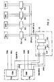
- FIG. 1 illustrates a computer system with function blocks representing a computer card, i.e., computational board CBA and CBB, on which there are two processor modules, general data processors GDPA and GDPB.
- the processor modules are VLSI components.
- the two processor modules GDPA and GDPB form a logical general data processor.
- One of the modules, under hardware or software control, is assigned the Master function and the other module the subordinate Checker function.
- the processor module GDPA is connected, via a local bus LB, to bus extension units BXUA and BXUB
- the processor module GDPB is connected, via a local bus LB, to bus extension units BXUC and BXUD.
- bus extension units BXUA and BXUC are connected to a system bus APA and each of the bus extension units BXUB and BXUD are connected to a further system bus APB.
- bus extension units BXUA and BXUC are connected to a system bus APA and each of the bus extension units BXUB and BXUD are connected to a further system bus APB.
- a nonredundant bus version (not shown) only one AP bus is connected via a BXU module to the processors.
- memory arrays MAA and MAB are connected to the system buses APA and APB.
- the bus extension units BXUA and BXUB are, furthermore, each connected via a communications line COM0 and COM1 to a parameter controller PC, and the bus extension units BXUC and BXUD are each connected via a communications line COM2 and COM3 to the said parameter controller PC.
- the parameter controller may be, for example, the Intel 8051 microprocessor.
- certain parameters of the computer card can be set from outside by means of analog or digital setting means as well as by means of stored data.
- the parameter controller is connected, via a buffer BUA, to the local bus LB of the first pair of processor modules GDPA and GDPB which are predefined as a Master pair and, via a buffer BUB, to the local bus LBB of the second processor modules GDPB.
- Figure 1 further shows two serial system support buses SSBA and SSBB and a set of support signal lines SSL.
- the parameter controllers PC of the computer cards are connected to either SSBA or SSBB: Redundant embodiments of each of the computer cards (e. g., processor means, memory means, input/output means) and the power supply modules are connected to separate serial system support buses.
- FIG. 1 shows an overall plan of two power supply modules PSA and PSB, both of essentially the same design.
- the power supply modules PSA and PSB exhibit two system support modules SSMA and SSMB, each of which is provided with a microprocessor, e.g., an Intel 8051. Outputs of the system support modules SSMA and SSMB are connected to the system support buses SSBA and SSBB respectively.
- the support signal lines SSL and their interconnections with the system and the power supply modules PSA/PSB are illustrated in figure 2 and 3 in more detail.
- the embodiment illustrated in Figure 2 contains four general data processors GDPA, GDPB, GDPC, GDPD in a fully redundant version.
- the embodiment illustrated in Figure 3 contains only two general data processors GDPA and GDPB and one power supply PSA. In this nonredundant computer configuration where only a MASTER / CHECKER system is present the same principles as described in Figure 2 may be used.
- the interconnecting line SSM-INTRA/SSM-INTRB allows a system interrupt signal to be emitted; this action can be induced, for example, by pressing an appropriate button on the system control panel. This signal causes the processor modules to start the system monitor program, for example for test functions, without resetting.
- a LOW signal can be used to indicate that the system will fail preferably after 2 milliseconds.
- initialization of all components under software or hardware control is carried out first during an INIT signal issued by the system support modules SSMA/SSMB.
- an identification phase during which the identities of the VLSI components are established.
- parameters are loaded into the appropriate registers of the VLSI components, preferably by means of the parameter controller PC, which is discribed in our Patent file "Arrangement for Loading the Parameters Into Active Modules in a Computer System” (our Dockel Number VPA 85 E 7421) assigned to Siemens Aktiengesellschaft and Intel Corporation.
- the parameters depend on the configuration of the system and on several controllable factors, and may differ from the values imposed in the first phase of initialization. Both phases are executed principally over the COM pins of the VLSI components, through serial loading of the registers in the components.
- the physical identification mechanism is controlled by a microcode implemented in the processor modules.
- Figure 2 further shows a circuit arrangement for the processing of interrupt and failure signals, in which the interrupt signal line SSM-INTRA and SSM-INTRB and the AC power failure signal line CPFA, CPFB of the two redundant power supply modules PSA and PSB are conducted through a register SC.
- the respective signal lines of each module for example CPFA and CPFB, are conducted through an OR element to an input of a register element SE1, which is supplied with the clock signal CLK at one clock input. Further clock pulse delays or synchronizations can be effected with the register elements SE2 and SE3, which are likewise supplied with the clock signal CLK.
- init signals issued by the SSMA and SSMB forces a system initialization. Two separate init signals are propagated to each system part. The two signals are interpreted differently for a cold and a warm start according to the following table. Init - Input System Reaction INITA INITB Warm-Init Cold-Init yes yes yes yes yes no no yes no yes no yes no no no no no no no no
- This strategy enables high-available systems on the one side to start after a cold start independantly of a single error in one of the SSMs. On the other side a restart after a warm init will only be done if neither SSMA nor SSMB does not show an error.
Abstract
A high reliability computer system comprising a system bus arrangement, an arrangement of processor modules in a MASTER/CHECKER pair located on said computer card and connected to said system bus arrangement, a power supply module supplying power to the computer system, said power supply module arrangement connecting to the computer system through a plurality of interconnecting lines, logic circuitry connected to said plurality of interconnecting lines for processing a plurality of system support signals transmitted by said power supply arrangement to the computer systems, to insure the integrity of said system support signals, and a interrupt signal line as part of said interconnecting lines.
Description
- This invention relates to electronic data processing systems and more particularly to redundant electronic computer systems with monitoring for secure processing of system support signals.
- For the operation of high-availability computer systems, to insure NON-STOP or reliable operation, it is necessary to at least duplicate all active computing components as well as the system support cards and the necessary interconnecting lines. In this connection it is necessary that the system support signals that are also duplicated, e.g., start, stop, INIT and interrupt; be checked for the possibility of false alarm. For example, if the power supply fails, interrupt signals are sent to the computer cards in order the achieve a well-defined stop condition in the processing of data without the complete loss of data present in the system. However, as a result of differences in delay time these interrupts may arrive at different times and thus yield contradictory information.
- Also, when the system is started, it is also necessary to evaluate correctly the initialization signals coming from the power supply modules in such a manner to ascertain that both power supply modules are functioning properly, even through operation will initially be carried on with one of the power supply modules.
- It is an object of this invention to create a computer system with logical monitoring for the secure processing of system support signals, such as start, stop and interrupt, wherein the system support signals, which are transmitted over separate interconnecting lines in the computer system, can influence the system only under well-defined preconditions.
- Briefly stated in accordance with one aspect of the invention the aforementioned objects are achieved by providing a high reliable computer system comprising a system bus arrangement, an arrangement of processor modules in a MASTER / CHECKER pair located on said computer card and connected to said system bus arrangement, a power supply module supplying power to the computer system, said power supply module arrangement connecting to the computer system through a plurality of interconnecting lines, logic circuitry connected to said plurality of interconnecting lines for processing a plurality of system support signals transmitted by said power supply arrangement to the computer systems, to insure the integrity of said system support signals, and a interrupt signal line as part of said interconnecting lines.
- Briefly stated in accordance with a further aspect of the invention the aforementioned objects are achieved by providing a redundant computer system including a redundant system bus arrangement of two essentially identical system buses, a redundant arrangement of processor modules in two essentially identical MASTER / CHECKER pairs located on said computer card and connected to the redundant system bus arrangement and the redundant module bus arrangement, a redundant power supply module arrangement of two essentially identical power supply modules supplying power to the computer system, the redundant power supply module arrangement connecting to the computer system through a plurality of redundant interconnecting lines, and logic circuitry connected to the plurality of interconnecting lines for processing a plurality of system support signals transmitted by the redundant power supply arrangement to the computer system, to insure the integrity of said system support signals.
- This arrangement in accordance with the invention insures that the system support signals are, in an advantageous manner, first either buffered by being placed in temporary storage in the case of an interrupt, or checked for plausibility or integrity in the case of INIT. In the case of buffering of the interrupt signal, it is made certain that data processing in each of the processor modules, which operate in parallel, is stopped in the same well-defined stop condition, since a repetition cannot take place until the next system clock pulse.
- While the specification concludes with claims particularly pointing out and distinctly claiming the subject matter which is regarded as the invention, it is believed that the invention will be better understood from the following description of the preferred embodiment taken in conjunction with the accompanying drawings in which:
- Figure 1 shows a simplified functional block diagram of an embodiment of a computer system;
- Figure 2 shows a circuit diagram relating to the signal lines for interrupt and failure signals and a register for a redundant computer system;
and - Figure 3 shows a nonredundant version of the diagram shown in Figure 2.
- Figure 1 illustrates a computer system with function blocks representing a computer card, i.e., computational board CBA and CBB, on which there are two processor modules, general data processors GDPA and GDPB. Like most of the computer modules mentioned in what follows, the processor modules are VLSI components. The two processor modules GDPA and GDPB form a logical general data processor. One of the modules, under hardware or software control, is assigned the Master function and the other module the subordinate Checker function. In the present preferred circuit, the processor module GDPA is connected, via a local bus LB, to bus extension units BXUA and BXUB, and the processor module GDPB is connected, via a local bus LB, to bus extension units BXUC and BXUD. Each of the bus extension units BXUA and BXUC are connected to a system bus APA and each of the bus extension units BXUB and BXUD are connected to a further system bus APB. In a nonredundant bus version (not shown) only one AP bus is connected via a BXU module to the processors.
- In a further function block, not shown in more detail, memory arrays MAA and MAB are connected to the system buses APA and APB.
- The bus extension units BXUA and BXUB are, furthermore, each connected via a communications line COM0 and COM1 to a parameter controller PC, and the bus extension units BXUC and BXUD are each connected via a communications line COM2 and COM3 to the said parameter controller PC. The parameter controller may be, for example, the Intel 8051 microprocessor. At further inputs of the parameter controller PC, certain parameters of the computer card can be set from outside by means of analog or digital setting means as well as by means of stored data. The parameter controller is connected, via a buffer BUA, to the local bus LB of the first pair of processor modules GDPA and GDPB which are predefined as a Master pair and, via a buffer BUB, to the local bus LBB of the second processor modules GDPB.
- Also in Figure 1, on the right-hand side, there are function blocks representing the input-output module I/OA and I/OB of the computer system described here, the circuitry not being treated in detail at this point. This I/O modules accomplishes the connection of the computer system to peripherals PM by means of well-defined communications protocols, e.g., LAN, etc.
- Figure 1 further shows two serial system support buses SSBA and SSBB and a set of support signal lines SSL. The parameter controllers PC of the computer cards are connected to either SSBA or SSBB: Redundant embodiments of each of the computer cards (e. g., processor means, memory means, input/output means) and the power supply modules are connected to separate serial system support buses.
- The bottom part of Figure 1 shows an overall plan of two power supply modules PSA and PSB, both of essentially the same design. In addition to the DC power supply connections, the power supply modules PSA and PSB exhibit two system support modules SSMA and SSMB, each of which is provided with a microprocessor, e.g., an Intel 8051. Outputs of the system support modules SSMA and SSMB are connected to the system support buses SSBA and SSBB respectively.
- The support signal lines SSL and their interconnections with the system and the power supply modules PSA/PSB are illustrated in figure 2 and 3 in more detail. The embodiment illustrated in Figure 2 contains four general data processors GDPA, GDPB, GDPC, GDPD in a fully redundant version. The embodiment illustrated in Figure 3 contains only two general data processors GDPA and GDPB and one power supply PSA. In this nonredundant computer configuration where only a MASTER / CHECKER system is present the same principles as described in Figure 2 may be used.
- The interconnecting line SSM-INTRA/SSM-INTRB allows a system interrupt signal to be emitted; this action can be induced, for example, by pressing an appropriate button on the system control panel. This signal causes the processor modules to start the system monitor program, for example for test functions, without resetting.
- Over the interconnecting line CPFA/CPFB, the system is notified of an interruption in the AC line power inputs to the power supply module PSA/PSB. For example, a LOW signal can be used to indicate that the system will fail preferably after 2 milliseconds.
- After the system is switched on, i.e., cold start, or just part of the system is restarted, i.e., a warm start, initialization of all components under software or hardware control is carried out first during an INIT signal issued by the system support modules SSMA/SSMB. There follows an identification phase, during which the identities of the VLSI components are established. Next, in the parameter loading phase, parameters are loaded into the appropriate registers of the VLSI components, preferably by means of the parameter controller PC, which is discribed in our Patent file "Arrangement for Loading the Parameters Into Active Modules in a Computer System" (our Dockel Number VPA 85 E 7421) assigned to Siemens Aktiengesellschaft and Intel Corporation. The parameters depend on the configuration of the system and on several controllable factors, and may differ from the values imposed in the first phase of initialization. Both phases are executed principally over the COM pins of the VLSI components, through serial loading of the registers in the components.
- The physical identification mechanism, with appropriate commands, is controlled by a microcode implemented in the processor modules.
- Figure 2 further shows a circuit arrangement for the processing of interrupt and failure signals, in which the interrupt signal line SSM-INTRA and SSM-INTRB and the AC power failure signal line CPFA, CPFB of the two redundant power supply modules PSA and PSB are conduced through a register SC. The respective signal lines of each module, for example CPFA and CPFB, are conduced through an OR element to an input of a register element SE1, which is supplied with the clock signal CLK at one clock input. Further clock pulse delays or synchronizations can be effected with the register elements SE2 and SE3, which are likewise supplied with the clock signal CLK.
- As described before init signals issued by the SSMA and SSMB forces a system initialization. Two separate init signals are propagated to each system part. The two signals are interpreted differently for a cold and a warm start according to the following table.
Init - Input System Reaction INITA INITB Warm-Init Cold-Init yes yes yes yes yes no no yes no yes no yes no no no no - This strategy enables high-available systems on the one side to start after a cold start independantly of a single error in one of the SSMs. On the other side a restart after a warm init will only be done if neither SSMA nor SSMB does not show an error.
- It will now be understood that there has been disclosed a new computer system with logical monitoring for secure processing of system support signals. As will be evident from the foregoing description, certain aspects of the invention are not limited to the particular details of the examples illustrated, and it is therefore contemplated that other modifications or applications will occur to those skilled in the art. It is accordingly intended that the claims shall cover all such modifications and applications as do not depart from the true spirit and script of the invention.
Claims (4)
1. A computer system comprising:
a system bus arrangement;
an arrangement of processor modules in a MASTER / CHECKER pair located on said computer card and connected to said system bus arrangement;
a power supply module supplying power to the computer system;
said power supply module arrangement connecting to the computer system through a plurality of interconnecting lines;
logic circuitry connected to said plurality of interconnecting lines for processing a plurality of system support signals transmitted by said power supply arrangement to the computer systems, to insure the integrity of said system support signals; and
a interrupt signal line and/or AC power failure signal line as part of said interconnecting lines.
2. A redundant computer system comprising:
a redundant system bus arrangement of at least two essentially identical system buses;
a redundant arrangement of processor modules in two essentially identical MASTER / CHECKER pairs located on said computer card and connected to said redundant system bus arrangement and said redundant module bus arrangement;
a redundant power supply module arrangement of two essentially identical power supply modules supplying power to the computer system;
said redundant power supply module arrangement connecting to the computer system through a plurality of redundant interconnecting lines;
logic circuitry connected to said plurality of interconnecting lines for processing a plurality of system support signals transmitted by said redundant power supply arrangement to the computer systems, to insure the integrity of said system support signals; and
a redundant interrupt signal line arrangement of two essentially identical interrupt signal lines as part of said redundant interconnecting lines.
3. A redundant computer system in accordance with claim 2 further comprising:
a redundant AC power failure signal line arrangement of two essentially identical AC power failure signal lines as part as said redundant interconnecting lines; and
each said power supply module, including a respective circuit arrangement having a clock input as a part thereof connecting to the respective interrupt signal line and the respective AC power failure signal line, repeats by means of said respective circuit arrangement, the respective system support signals to the computer system upon impressing a clock pulse to said clock input of said circuit arrangement.
4. A redundant computer system in accordance with claim 2 further comprising:
means for producing a redundant INIT signal issued by the system support modules and evaluating the INIT signal in a microprocessor for system operating with one of the operational power supplies.
means for producing a redundant INIT signal issued by the system support modules and evaluating the INIT signal in a microprocessor for system operating with one of the operational power supplies.
Applications Claiming Priority (2)
| Application Number | Priority Date | Filing Date | Title |
|---|---|---|---|
| US12369987A | 1987-11-23 | 1987-11-23 | |
| US123699 | 1987-11-23 |
Publications (2)
| Publication Number | Publication Date |
|---|---|
| EP0317827A2 true EP0317827A2 (en) | 1989-05-31 |
| EP0317827A3 EP0317827A3 (en) | 1990-12-27 |
Family
ID=22410330
Family Applications (1)
| Application Number | Title | Priority Date | Filing Date |
|---|---|---|---|
| EP19880118676 Withdrawn EP0317827A3 (en) | 1987-11-23 | 1988-11-09 | Computer system with logical monitoring for secure processing of system support signals |
Country Status (1)
| Country | Link |
|---|---|
| EP (1) | EP0317827A3 (en) |
Citations (2)
| Publication number | Priority date | Publication date | Assignee | Title |
|---|---|---|---|---|
| US4234920A (en) * | 1978-11-24 | 1980-11-18 | Engineered Systems, Inc. | Power failure detection and restart system |
| US4597084A (en) * | 1981-10-01 | 1986-06-24 | Stratus Computer, Inc. | Computer memory apparatus |
-
1988
- 1988-11-09 EP EP19880118676 patent/EP0317827A3/en not_active Withdrawn
Patent Citations (2)
| Publication number | Priority date | Publication date | Assignee | Title |
|---|---|---|---|---|
| US4234920A (en) * | 1978-11-24 | 1980-11-18 | Engineered Systems, Inc. | Power failure detection and restart system |
| US4597084A (en) * | 1981-10-01 | 1986-06-24 | Stratus Computer, Inc. | Computer memory apparatus |
Non-Patent Citations (1)
| Title |
|---|
| IEEE MICRO, vol. 4, no. 6, December 1984, pages 34-43, New York, US; R. EMMERSON et al.: "Fault tolerance achieved in VLSI" * |
Also Published As
| Publication number | Publication date |
|---|---|
| EP0317827A3 (en) | 1990-12-27 |
Similar Documents
| Publication | Publication Date | Title |
|---|---|---|
| US5255367A (en) | Fault tolerant, synchronized twin computer system with error checking of I/O communication | |
| EP0260625B1 (en) | Method for bumpless changeover from active units to back-up units in computer equipment and a device for carrying out the method | |
| EP0306252B1 (en) | Fault tolerant computer system input/output interface | |
| EP0306244B1 (en) | Fault tolerant computer system with fault isolation | |
| US5249187A (en) | Dual rail processors with error checking on I/O reads | |
| EP0306209B1 (en) | Dual rail processors with error checking at single rail interfaces | |
| US7890797B2 (en) | Vehicle including a processor system having fault tolerance | |
| JP3206006B2 (en) | Duplex bus control method and device | |
| US6434712B1 (en) | Method and apparatus for fault tolerant execution of computer programs | |
| US4860196A (en) | High-availability computer system with a support logic for a warm start | |
| US6532545B1 (en) | Apparatus for swapping, adding or removing a processor in an operating computer system | |
| US5617546A (en) | Data bus architecture compatible with 32-bit and 64-bit processors | |
| US5048022A (en) | Memory device with transfer of ECC signals on time division multiplexed bidirectional lines | |
| EP0341511A2 (en) | High-availability computer system with a predefinable configuration of the modules | |
| US5115511A (en) | Arrangement for loading the parameters into active modules in a computer system | |
| US20040193735A1 (en) | Method and circuit arrangement for synchronization of synchronously or asynchronously clocked processor units | |
| EP0317827A2 (en) | Computer system with logical monitoring for secure processing of system support signals | |
| EP0306855A2 (en) | Arrangement for loading the parameters into active modules in a computer system | |
| EP0317828A2 (en) | Serial bus in a computer system for internal system communications | |
| JPS5843775B2 (en) | Processor backup system | |
| GB2146810A (en) | Achieving redundancy in a distributed process control system | |
| JPH07114521A (en) | Multimicrocomputer system | |
| JP2000347706A (en) | Plant controller | |
| JP2000242317A (en) | Programmable controller | |
| JPH1011102A (en) | Duplex system |
Legal Events
| Date | Code | Title | Description |
|---|---|---|---|
| PUAI | Public reference made under article 153(3) epc to a published international application that has entered the european phase |
Free format text: ORIGINAL CODE: 0009012 |
|
| AK | Designated contracting states |
Kind code of ref document: A2 Designated state(s): CH DE ES FR GB IT LI |
|
| PUAL | Search report despatched |
Free format text: ORIGINAL CODE: 0009013 |
|
| AK | Designated contracting states |
Kind code of ref document: A3 Designated state(s): CH DE ES FR GB IT LI |
|
| STAA | Information on the status of an ep patent application or granted ep patent |
Free format text: STATUS: THE APPLICATION IS DEEMED TO BE WITHDRAWN |
|
| 18D | Application deemed to be withdrawn |
Effective date: 19910531 |