EP0316943A2 - Semiconductor integrated circuit having a plurality of oscillation circuits - Google Patents
Semiconductor integrated circuit having a plurality of oscillation circuits Download PDFInfo
- Publication number
- EP0316943A2 EP0316943A2 EP88119225A EP88119225A EP0316943A2 EP 0316943 A2 EP0316943 A2 EP 0316943A2 EP 88119225 A EP88119225 A EP 88119225A EP 88119225 A EP88119225 A EP 88119225A EP 0316943 A2 EP0316943 A2 EP 0316943A2
- Authority
- EP
- European Patent Office
- Prior art keywords
- oscillation
- circuit
- clock
- semiconductor integrated
- signals
- Prior art date
- Legal status (The legal status is an assumption and is not a legal conclusion. Google has not performed a legal analysis and makes no representation as to the accuracy of the status listed.)
- Granted
Links
Images

Classifications
-
- G—PHYSICS
- G06—COMPUTING; CALCULATING OR COUNTING
- G06F—ELECTRIC DIGITAL DATA PROCESSING
- G06F1/00—Details not covered by groups G06F3/00 - G06F13/00 and G06F21/00
- G06F1/04—Generating or distributing clock signals or signals derived directly therefrom
- G06F1/08—Clock generators with changeable or programmable clock frequency
Landscapes
- Engineering & Computer Science (AREA)
- Theoretical Computer Science (AREA)
- Physics & Mathematics (AREA)
- General Engineering & Computer Science (AREA)
- General Physics & Mathematics (AREA)
- Microcomputers (AREA)
- Power Sources (AREA)
Abstract
Description
- The present invention relates to a semiconductor integrated circuit device, and more specifically to technology that can be effectively utilized for a semiconductor integrated circuit device such as a one-chip microcomputer having, for example, a time-keeping function.
- In an electronic desk-top calculator constituted by a microcomputer and semiconductor integration circuits, provision is made of an oscillation circuit using an oscillator such as quartz oscillator to produce clock signals (hereinafter simply referred to as system clocks) for operating the system. When such a data processing system is intermittently operated, the original oscillation is stopped and operations of the microprocessor and memory are temporarily stopped in order to reduce the consumption of electric power. For this purpose, a halt function is provided to stop the system clock upon receipt of a control signal from an external unit or an instruction from the microprocessor.
- In the semiconductor integrated circuit device such as a microcomputer having timekeeping function, however, the timekeeping function cannot be stopped if the oscillation circuit is commonly utilized for keeping the time and for the original oscillation; i.e., it is not allowed to add the holding function. Therefore, there has been proposed a microcomputer mounting a quartz oscillation circuit of 32.768 KHz for timekeeping and a cheaply constructed CR oscillation circuit or an oscillation circuit using a ceramic oscillator for the original oscillation (about 4 MHz). The microcomputer equipped with such two oscillation circuits has been described, for example, in "Hitachi 4-Bit 1-Chip Microcomputer System, HMCS 40 Series, LCD-III, User's Manual", third edition, No. 4, Hitachi, Ltd., June, 1984, pp. 4 and 24-25.
- In the microcomputer, when the original oscillation operation of the above-mentioned high frequency is stopped under the holding condition, the oscillation circuit on the side of the original oscillation must be energized at least after every second to supply a system clock to the microprocessor in order to realize the timekeeping function. It was therefore found by the present inventors that a stabilization waiting time becomes relatively long before the oscillation is resumed, and unstable oscillation operation of a high frequency takes place during that moment consuming large amounts of electric power.
- It was further studied by the present inventors to form system clocks of a low frequency by switching into an oscillation output of the oscillation circuit for timekeeping during the halting operation (subactive). In this case, it was found by the present inventors that frequencies of basic clock pulses for timekeeping and of basic clock pulses for the system do not establish a ratio of an integer number such as about 32 KHz and about 4 MHz; i.e., oscillation operations are performed out of synchronism. Therefore, synchronism is not maintained when the two clocks are to be switched (active/subactive), and extremely narrow pulses SP and undesirably wide pulses WP are formed as system clocks as shown in Fig. 6. As a result, the system may undergo erroneous operation when the clocks are to be switched.
- The object of the present invention is to provide a semiconductor integrated circuit device which is designed to operate stably consuming reduced amounts of electric power.
- The above and other objects as well as novel features of the present invention will become obvious from the description of the specification and the accompanying drawings.
- Among the inventions disclosed in the present application, a representative example will now be described briefly. That is, when oscillation output signals are selectively transmitted to a clock generating circuit via a multiplexer, the oscillation output signals being generated by a first oscillation circuit whose oscillation operation of a relatively high frequency is controlled by predetermined control signals and by a second oscillation circuit which steadily performs the oscillation operation of a relatively low frequency, the clock-generating operation is started in synchronism with the oscillation output that is switched via a mode which once stops the operation of the clock generating circuit.
- For example, there are provided a clock switching circuit, a flag which designates which clock be used by the clock switching circuit, and a flag which indicates whether the clock selected by the clock switching circuit be supplied to the system or not, and wherein the flags are set according to an interrupt signal or a program instruction, a mode which once shuts off all clocks (hereinafter referred to as stop mode or watch mode) is necessarily passed through when an ordinary operation mode (hereinafter referred to as standard operation mode or active mode) is to be transferred to a mode of low power consumption (hereinafter referred to as low-power-consumption mode or subactive mode) or vice versa, and the clocks are switched during this moment.
- According to the above-mentioned means, operation of the oscillation circuit which performs oscillation operation at a relatively high frequency is stopped as required and when the clock frequency is to be switched, the clock-generating operation is resumed in synchronism with an oscillation frequency that is switched after the operation of the clock generating circuit is once stopped. When the clock pulses having dissimilar frequencies are to be switched, therefore, undesired hair-like clock pulses are not produced and the operation is carried out stably.
-
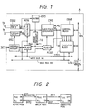
- Fig. 1 is a block diagram of an embodiment in which the present invention is adapted to a single-chip microcomputer;
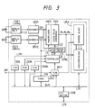
- Fig. 2 is a diagram explaining the condition of mode transition in a microcomputer to which the present invention is adapted;
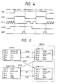
- Fig. 3 is a block diagram of another embodiment in which the present invention is adapted to the single-chip microcomputer;
- Fig. 4 is a diagram of waveforms for explaining the operation;
- Fig. 5 is a diagram of status transition for explaining an example of the operation; and
- Fig. 6 is a diagram of waveforms for explaining the operation for switching the clock pulses that can be taken into consideration prior to the present invention.
- An embodiment in which the invention is adapted to a single-chip microcomputer will now be described in conjunction with Figs. 1 and 2.
- Though there is no particular limitation, the circuit blocks surrounded by a chain line A are formed on a single semiconductor chip such as a single crystalline silicon substrate.
- The single-chip microcomputer according to this embodiment is equipped with two oscillation circuits consisting of an oscillation circuit OSC₁ for generating system clocks and an oscillation circuit OSC₂ for generating timekeeping clocks. The oscillation circuit OSC₁ is provided with a
ceramic oscillator 1a which is located on the external side and the oscillation circuit OSC₂ is provided with aquartz oscillator 1b which is located on the external side. - Original oscillation signals φOSC which constitute system clocks of 4 MHz generated by the oscillation circuit OSC₁ and original oscillation signals φCL which constitute timekeeping clocks of 32.768 KHz generated by the oscillation circuit OSC₂ are supplied to a multiplexer MPX where clocks of either side are selected depending upon the set condition of a flag FLG₁ that designates clocks and are supplied to a clock pulse generating circuit CPG.
- The clock pulse generating circuit CPG divides the frequency of oscillation signals φOSC or φCL supplied thereto via the multiplexer MPX or processes them to form several kinds of internal clocks φ₁, φ₂, φ₃, ..... having suitable frequencies and different phases. The internal clocks φ₁, φ₂, φ₃, ..... are supplied to a control block CONT which consists of a ROM that stores programs, a program counter that successively reads instructions from the program ROM, and an instruction decoder that decodes the instruction codes that are read out to form control signals for the circuits in the microcomputer, and are further supplied to an execution block EXEC which consists of various registers, ALU (arithmetic logic unit) and RAM that serves as a work area. The program counter in the control block CONT and the execution block EXEC are connected to an input/output port I/O via a bus BUS.
- In this embodiment, there are provided a stop flag FLG₂ that can be set by a suitable instruction called stop instruction, and a status signal that indicates the content of the stop flag FLG₂ is supplied to the clock pulse generating circuit CPG to control the gate that is provided at the inlet thereof. Concretely speaking, when "1" is set to the flag FLG₂ due to the stop instruction, the oscillation circuit OSC₁ for generating system clocks ceases to oscillate, and a mode (hereinafter referred to as stop mode or watch mode) is established in which no clock is supplied from the multiplexer MPX to the clock pulse generating circuit CPG and none of the internal clocks φ₁, φ₂, φ₃, ..... are generated. Therefore, the system is under the stop condition in which it does not operate at all.
- To get out of the stop mode, on the other hand, there is provided a timer interrupt circuit TIC which generates a timer interrupt singal INT₁ based on a signal from a frequency-dividing circuit DVD that divides the frequency of original oscillation signals φCL that constitute timekeeping clocks. The interrupt signal INT₁ from the timer interrupt circuit TIC is supplied to the stop flag FLG₂ to clear it to "0", and is also supplied to the flag FLG₁ to set it. After the flag FLG₁ set, the multiplexer MPX which receives the status signal supplies to the clock pulse generating circuit CPG the original oscillation signal φCL of timekeeping clock instead of the original oscillation signal φOSC of system clock. Therefore, the system is operated by the clocks of a low frequency formed based on the signals φCL and assumes the low-power-consumption mode (subactive mode) for carrying out the operation such as addition and the like for timekeeping function.
- In this embodiment, furthermore, an external interrupt control circuit EIC is provided to receive an interrupt signal INT₂ from the external unit. When an external interrupt signal INT₂ is input in the stop mode (watch mode), the oxcillation circuit OSC₁ starts the oscillation, and the stop flags FLG₂ and FLG₁ are cleared. When the flag FLG₁ is cleared, the multiplexer MPX supplies original oscillation signals φOSC of system clocks to the clock pulse generating circuit CPG. Therefore, the system assumes the standard operation mode (active mode) in which it is operated at high speeds by the clocks of a high frequency formed by the clock pulse generating circuit CPG.
- Fig. 2 shows the transition condition of mode according to the above embodiment.
- According to the above embodiment as will be obvious from Fig. 2, the stop instruction is executed at the final stage of execution of an ordinary system program or at the final stage of a program for the timekeeping operation in the low-power-consumption mode, so that the system is transferred to the stop mode (watch mode) in which the system clocks are all extinguished. Thereafter, the system gets out of the stop mode (watch mode) in response to the interrupt and assumes the low-power-consumption mode (subactive mode) or the standard operation mode (active mode) depending upon the content of the flag FLG₁.
- Therefore, when the system is transferred from the standard operation mode to the low-power-consumption mode or vice versa, the clocks are not suddenly changed from φOSC to φCL or from φCL to φOSC. Therefore, extremely short clock pulses are not formed and the system is not erroneously operated.
- In the above-mentioned embodiment, the stop mode is transferred again to the low-power-consumption mode in case the timer interrupt INT₁ is input prior to the input of interrupt signal INT₂ from the external unit during the stop mode that has transferred from the low-power-consumption mode.
- In the clock switching circuit of the above embodiment, furthermore, the flag FLG₁ is connected to the internal buses WB, RB to set the content of the flag FLG₁ depending upon the instruction. In executing the stop instruction, therefore, the content of the flag FLG₁ iS arbitrarily set in advance, and the system is transferred to a desired mode of either a first mode such as the standard operation mode or a second mode such as the low-power-consumption mode when the next interrupt signal has entered. In the above-mentioned embodiment, operation of the oscillation circuit OSC₁ on the system clock side is stopped during the stop mode and the low-power-consumption mode. It is, however, also allowable to transfer the system from the standard operation mode to the low-power-consumption mode or vice versa by controlling the switching of clocks and the interrupt and supply of clocks while the oscillation circuit is in operation.
- In the above-mentioned embodiment, furthermore, the flags FLG₁ and FLG₂ may be independently constituted by themselves, or a bit in the control register or any bit in the RAM may be allotted thereto.
- According to the above-mentioned embodiment as described above, the microcomputer that includes two oscillation circuits of dissimilar oscillation frequencies is provided with a clock switching circuit, a flag that designates which clocks be used based on the clock switching circuit, and a flag which indicates whether the clocks selected by the clock switching circuit be supplied to the system or not, and the flags are set depending on the interrupt signal or the program instruction. When the system is transferred from the ordinary operation mode to the low-power-consumption mode or vice versa, the stop mode (watch mode) is passed through to shut off all clocks, and the clocks are switched during this moment. Therefore, all of the clocks are once extinguished at the time of switching the clocks, and synchronism is maintained among the clocks. Hence, the system does not operate erroneously and is transferred from the standard operation mode (active mode) to the low-power-consumption mode (subactive mode) or vice versa. Accordingly, clocks are switched without adversely affecting the operation of the system, and the low-power-consumption mode is realized.
- In the foregoing was concretely described the invention accomplished by the present inventors by way of an embodiment. The present invention, however, is in no way limited to the above-mentioned embodiment only but can be modified in a variety of other ways without departing from the spirit and scope of the invention. Though the above embodiment has dealt with the microcomputer provided with two oscillation circuits for generating the clocks, the invention can also be adapted to the one that generates three or more kinds of clocks. According to the present invention, furthermore, the mode is controlled using two flags, i.e., a stop flag that is set by the stop instruction and that indicates the stop condition of all clocks and a clock designation flag which indicates the kind of clocks to be supplied after the clock stop condition is released, i.e., which indicates the direction of mode to which the system will transfer after the clock stop condition is released. In a system in which the two operation modes are alternatingly repeated, however, the flag for designating the clocks may be eliminated, and the multiplexer MPX may be switched based on the stop instruction or the interrupt.
- Fig. 3 is a block diagram of another embodiment of the case when the present invention is adapted to a single-chip microcomputer, wherein the circuit blocks surrounded by a broken line are formed on a semiconductor substrate such as of single crystalline silicon by the widely known technology for fabricating the semiconductor integrated circuits, though there is no particular limitation.
- The microcomputer according to this embodiment is provided with a first oscillation circuit (original oscillation circuit) OSC1 for generating system clocks and a second oscillation circuit OSC2 for producing reference time pulses for timekeeping. The first oscillation circuit OSC1 is provided with, for example, a ceramic oscillator X1 on the outside to oscillate at a frequency which is as relatively high as about 4 MHz. To reduce the consumption of electric power, oscillation operation of the oscillation circuit OSC1 is controlled by control signals C3 that will be described later. The second oscillation circuit OSC2 is provided with a quartz oscillator X2 to oscillate at a frequency which is as relatively low as 32.768 KHz. The oscillation circuit OSC2 is provided for performing the timekeeping operation and performs oscillation operation steadily.
- The output signals of the oscillation circuits OSC1 and OSC2 are converted into basic clock pulses CK1 and CK2 through frequency-dividing circuit DiV1 and DiV2 that also work to shape waveforms. The basic clock pulses CK1 and CK2 are supplied to the clock pulse generating circuit CPG via the multiplexer MPX which is switched by the control circuit CONT. The multiplexer MPX selectively transmits the basic clock pulses CK1 or CK2 to the clock pulse generating circuit CPG depending upon the operation mode that will be described later.
- The clock pulse generating circuit CPG divides the frequency of the basic clock pulses CK1 or CK2 that are input via the multiplexer MPX or processes them to form a plurality of system clocks φ1 to φ3, etc. having different phases.
- The system clocks φ to φ3, etc. are supplied to a control block which consists of a ROM (read-only memory) that stores programs, a program counter that successively reads instructions from the program ROM, and an instruction decoder that decodes the instruction codes that are read out to form control signals for the circuits in the microcomputer, and are supplied to an execution block which consists of various registers, ALU (arithmetic logic operation unit) and RAM (random access memory) that serves as a work area.
- A microcomputer CPU is constituted by the above-mentioned control block and the execution block. The program counter in the control block and the execution block are connected via buses BUS to an input/output port I/O, a timer circuit TM, and various control flags. The internal buses BUS are made up of address bus, data bus and control bus.
- The clock pulse generating circuit CPG of this embodiment does not steadily form the above-mentioned system clocks φ1 to φ3, etc. in response to the basic clock pulses CK1 or CK2 input through the multiplexer, and is controlled for its operation by the control signals C2′. In order that the system clocks φ to φ3, etc. are generated in synchronism with the switched basic clock pulses CK1 or CK2, the control signals C2 formed by the controller CONT are passed through the synchronizing circuit SYNC to maintain synchronism with the basic clock pulses CK1 or CK2.
- The basic clock pulses CK2 for timekeeping are supplied to the timekeeping circuit TM which divides the frequency of the basic clock pulses CK2 to form time pulses such as 1-
second pulses 1S. Thetime pulses 1S are supplied to an interrupt flag INTF to serve as a factor of interrupt. The interrupt processing by thetime pulse 1S designates timekeeping operation for the control block in the CPU. For example, if there develops interrupt due to thetime pulse 1S, the control block in the CPU reads the data of seconds stored in the RAM that serves as a work area, adds +1 thereto, and writes it onto the RAM as new data of a unit of a second. In this case, if there is a carry, +1 is added to the data of minute in the same manner as described above. Likewise, if there is a carry, the data of hour, the data of day or the data of week is increased. As described above, the time-keeping operation is realized by fundamentally effecting the interrupt after every second to increase the data of second, and by adding +1 to other data depending upon the presence or absence of carry. - It is also allowable to carry out the timekeeping operation in shorter than one second by inputting suitable offset data from the internal buses BUS to the timekeeping circuit TM and generating the
time pulse 1S at a period of shorter than 1 second. - According to this embodiment, there is provided a flag REG that can be set by a suitable instruction called stop instruction STOP, and a status signal LPM (low power mode) that represents the content of the stop flag REG is supplied to the control circuit CONT. The signal LPM consists of two bits, i.e., a stop STP and a stand-by signal SBY to produce three statuses consisting of the aforementioned active mode, a watch mode and a subactive mode that will be described later.
- In the active mode, the flag REG is cleared as shown in the waveform diagram of Fig. 4 and in the status transition diagrams of Fig. 5. In response to the low level of signals STP and SBY, the control circuit CONT places the oscillation circuit OSC1 under the oscillating condition upon receipt of control signal C3, and switches the multiplexer MPX to the side of the basic clock pulses CK1. The clock pulse generating circuit CPG therefore generates system clocks φCPU (φ1 to φ3, etc.) of a high frequency fcyc corresponding to the basic clock pulses CK1.
- In such an active mode, if the stop instruction STOP is executed and the signals STP and SBY are set to the high level relative to the stop flag REG, the control circuit CONT designates operation for transferring the system from the active mode to the watch mode depending upon the high level (logic "1"). That is, in the watch mode, the oscillation circuit OSC1 stops the oscillation operation and the clock pulse generating circuit CPG stops its operation, too. Therefore, the system clocks φCPU (φ to φ3, etc.) are not supplied to the CPU. In the watch mode, there are produced neither the system clocks φCPU nor the clock pulses φPER for peripheral circuits. However, the clock pulses φCLK that serve as time bases for maintaining the timekeeping function have a low frequency fSUB based on the basic clock pulses CK2.
- A flag LSON designates the low-speed-on condition and means that it is on the upper status in the transition diagram of Fig. 5 when it has the logic "0", and means that it is on the lower status when it has the logic "1". As will be described later, this is used as an indication when the system is transferred from the watch mode to other active mode or subactive mode. For example, when the timekeeping function only is to be carried out, the flag LSON is set to the logic "1" prior to executing the stop instruction STOP.
- In the watch mode as described above, the oscillation circuit OSC2 for timekeeping is under the oscillating condition, and the timekeeping circuit TM only is in operation in response thereto. Therefore, other circuits assume the mode in which the current is not logically consumed.
- In this embodiment, when the timekeeping function only is to be carried out by setting the logic "1" to the flag LSON, the interrupt flag INTF makes access to the control circuit CONT when a 1-second pulse IS is produced from the timekeeping circuit TM and designates the change of mode into the subactive mode. In response thereto, the control circuit CONT switches the multiplexer MPX to the basic clock pulses CK2. The synchronizing circuit SYNC generates control signals C2′ in synchronism with the switched basic clock pulses CK2, so that the clock pulse generating circuit CPG resumes its operation. Therefore, the clock pulse generating circuit CPG generates system clocks φCPU (φ1 to φ3, etc.) for the CPU of a low frequency fSUB based on the basic clock pulses CK2 for timekeeping. Concretely speaking, in resuming the operation of the clock pulse generating circuit CPG, the control signals C2′ for controlling the logic gate that transmits the basic clock pulses CK2 to the input of the clock pulse generating circuit CPG, are generated by the synchronizing circuit SYNC in synchronism with the clock pulses CK2. Therefore, narrow pulses or wide pulses are not generated in the system clocks φCPU (φ1 to φ3, etc.) that are formed by the clock pulse generating circuit CPG.
- The interrupt flag INTF, on the other hand, actuates the control block of the microprocessor CPU and adds +1 to carry out the timekeeping operation as described above. The system returns again to the watch mode by the execution of the stop instruction STOP that is inserted in the interrupt processing program at the final stage of the timekeeping operation.
- As described above, the system clocks φCPU are formed by utilizing basic clock pulses CK2 that are formed by the oscillation circuit OSC2 for timekeeping while the timekeeping operation is being carried out, and the oscillation circuit OSC1 of a high frequency is not at all operated to add +1 using the microprocessor CPU maintaining a relatively short time interval such as one second as described above. Therefore, the current is not wastefully consumed from the start of oscillation until the oscillation is stabilized.
- There exist three statuses as described below when the system returns to the active mode.
- One of them will now be described. When the system is in the watch mode under the condition where the flag LSON is set to the logic "1", the interrupt flag INTF is started from the external interrupt terminal INT and the system is once transferred to the subactive mode in a manner as described above. The interrupt flag INTF informs the execution block of the microprocessor CPU of the fact that the interrupt is due to an external factor, clears the flag LSON to the logic "0" by the interrupt processing so that the interrupt processing in the first stage is finished. Owing to the execution of the stop instruction STOP when the interrupt processing is finished, the system transfers to the watch mode (LSON = "0") on the upper side in the status transition diagram of Fig. 5. The interrupt flag INTF is started again from the external interrupt terminal INT, so that the active mode is assumed. In this case, the control circuit CONT generates control signals C3 so that the oscillation circuit OSC1 starts to oscillate, and the multiplexer MPX is switched to the side of the basic clock pulses CK1. After the oscillation of the oscillation circuit OSC1 is stabilized, the clock pulse generating circuit CPG resumes the operation in synchronism with the basic clock pulses CK1. Therefore, the oscillation circuit OSC1 undergoes the oscillation, and the system clocks φCPU (φ1 to φ3, etc.) supplied to the CPU and the clock pulses φPER for peripheral circuits have a high frequency fcyc according to the basic clock pulses CK1.
- As described above, with the flag DTON being set to the logic "1" instead of applying the external interrupt two times, the watch mode (LSON = "1") is automatically changed in the system to the watch mode (LSON = "0") through the subactive mode by the external interrupt of one time, and is returned to the active mode. In other words, when the flag DTON is set to the logic "1", the control circuit CONT automatically executes the operation for switching the clocks as described above.
- The remaining one stands for the case when the flag LSON is set to the logic "0" while the system is transferred from the active mode to the watch mode. In this case, the system is transferred to the active mode in response to one interrupt. This interrupt includes the interrupt by the timer circuit TM for the timekeeping operation. Attention, therefore, should be given to that switching from the watch mode to the active mode involves operation for starting the oscillation circuit OSC1 in a traditional manner.
- Further, a variety of flags for designating the operations of the control circuit CONT that switches the clocks in the above embodiment are connected to the internal buses BUS, such that the content of the flag is set depending upon the instructions. Therefore, by arbitrarily setting the content (LSON) of the flag in advance at the time of executing the stop instruction, the system can be transferred, when a next interrupt signal is input, to a desired mode of either the active mode such as the standard operation mode or the subactive mode which carries out the timekeeping operation only. With the flag DTON being set, furthermore, the watch mode can be automatically returned to the active mode by one time of external interrupt as described earlier.
- The functions and effects obtained from the above-mentioned embodiment of Fig. 3 are described below.
- (1) Oscillation output signals are selectively transmitted to a clock generating circuit via a multiplexer, the oscillation output signals being generated by the first oscillation circuit whose oscillation operation of a relatively high frequency is controlled according to predetermined control signals and by the second oscillation circuit which steadily carries out the oscillation operation at a relatively low frequency. Furthermore, the clock generating operation is started in synchronism with the oscillation outputs that are switched via an operation mode which once stops the operation of the clock generating circuit. In this constitution, oscillation operation at a relatively high frequency of the oscillation circuit is stopped as required, and operation of the clock generating circuit is once stopped when the clock frequency is to be changed and, then, the clock generating operation is resumed in synchronism with the oscillation frequency that is changed. When the clock pulses having dissimilar frequencies are to be switched, therefore, undesired hair-like clock pulses are not produced, and the operation is stably carried out.
- (2) The second oscillation circuit is used as an oscillation circuit for timekeeping, and system clocks are formed by the oscillation pulses for timekeeping in the low-power-consumption mode in which the first oscillation circuit is not in operation, such that the CPU carries out the timekeeping operation. Therefore, there is no need of starting the first oscillation circuit that is set to operate at a relatively high frequency maintaining a short interval of, for example, at least one second. This makes it possible to reduce the consumption of electric current that would be consumed in relatively large amounts by the first oscillation circuit from the start of the first oscillation circuit until the oscillation is stabilized. Therefore, the operation is stabilized and the consumption of electric power is reduced.
- In the foregoing was concretely described the invention accomplished by the present inventors by way of embodiments. The present invention, however, is in no way limited to the above-mentioned embodiments only but can be modified in a variety of other ways without departing from the spirit and scope of the invention. For example, operation of the oscillation circuit OSC1 on the side of the system clocks is stopped during the watch mode and the subactive mode. However, it is also allowable to stay in the low-power-consumption mode in which the oscillation circuit OSC1 is in operation but the clock generating circuit CPG is not in operation when the flag LSON has the logic "0" or even in the watch mode by providing other flags. Since there is no time for waiting for the start of the oscillation circuit OSC1, the watch mode can be switched to the active mode at a high speed. The flags in the aforementioned embodiments may be constituted independently by the flip-flop circuits, or a bit in the control register or a given bit in the RAM may be allotted thereto.
- The synchronizing circuit resumes the operation in synchronism with the basic clock pulses CK1 or CK2 obtained by switching the clock pulse generating circuit CPG, and generates the gate control signals that will be input to the clock pulse generating circuit CPG in synchronism with the above-mentioned switched basic clock pulses CK1 or CK2. Moreover, the synchronizing circuit may be constituted in various other forms. For example, the output unit of the clock pulse generating circuit CPG may be provided with a gate circuit to control the output timing thereof. Or, the flip-flop circuit constituting the clock pulse generating circuit may be forcibly reset and may then be released in synchronism with the basic clock pulse CK1 or CK2.
- The foregoing description has chiefly dealt with the case where the invention accomplished by the present inventors is adapted to a 1-chip microcomputer having the low-power-consumption mode in the field of art that serves as the background of the invention. The invention, however, is in no way limited thereto only but can be widely adapted to a variety of semiconductor integrated circuit devices that supply to the internal circuits in a switched manner a plurality of clock pulses having different oscillation frequencies asynchronously.
Claims (11)
a first oscillation circuit (OSC1) for producing signals of a first frequency;
a second oscillation circuit (OSC2) for producing signals of a second frequency different from said first frequency;
a clock generating circuit (CPG) for forming first clock signals or second clock signals based on the output signals of said first oscillation circuit (OSC1) or the output signals of said second oscillation circuit (OSC2);
data processing means (EXEC; CPU) whose operation is controlled based on said clock signals; and
control means (CONT) for controlling the output timing of said clock generating circuit (CPG);
wherein said control means (CONT) has a period in which a constant level signal is produced from the completion of production of said first clock signal to the start of production of said second clock signal, and the timing for producing the second clock signal is controlled to be in synchronism with the signal produced by the second oscillation circuit (OSC2).
a first frequency-dividing circuit (DIV1) for dividing the frequency of output signals of said first oscillation circuit (OSC1);
a second frequency-dividing circuit (DIV2) for dividing the frequency of output signals of said second oscillation circuit (OSC2); and
a multiplexer (MPX) for selectively supplying the output signals of said first frequency-dividing circuit (DIV1) or the output signals of said second frequency-dividing circuit (DIV2) to said clock generating circuit (CPG).
wherein said data processing means includes a CPU whose operation is controlled based on said clock signals; and
wherein said control means (CONT) does not produce a clock signal in the period from the completion of production of said first clock signal to the start of production of said second clock signal.
Applications Claiming Priority (2)
| Application Number | Priority Date | Filing Date | Title |
|---|---|---|---|
| JP293796/87 | 1987-11-20 | ||
| JP62293796A JP2614877B2 (en) | 1987-11-20 | 1987-11-20 | Semiconductor integrated circuit device |
Publications (3)
| Publication Number | Publication Date |
|---|---|
| EP0316943A2 true EP0316943A2 (en) | 1989-05-24 |
| EP0316943A3 EP0316943A3 (en) | 1990-03-21 |
| EP0316943B1 EP0316943B1 (en) | 1995-04-19 |
Family
ID=17799268
Family Applications (1)
| Application Number | Title | Priority Date | Filing Date |
|---|---|---|---|
| EP88119225A Expired - Lifetime EP0316943B1 (en) | 1987-11-20 | 1988-11-18 | Semiconductor integrated circuit having a plurality of oscillation circuits |
Country Status (5)
| Country | Link |
|---|---|
| EP (1) | EP0316943B1 (en) |
| JP (1) | JP2614877B2 (en) |
| KR (1) | KR0134780B1 (en) |
| DE (1) | DE3853615T2 (en) |
| HK (1) | HK27896A (en) |
Cited By (9)
| Publication number | Priority date | Publication date | Assignee | Title |
|---|---|---|---|---|
| EP0437224A2 (en) * | 1990-01-08 | 1991-07-17 | Matsushita Electric Industrial Co., Ltd. | Clock producing apparatus for PWM system digital analog converter use |
| EP0446958A2 (en) * | 1990-03-16 | 1991-09-18 | Nec Corporation | Single-chip microcumputer with clocksignal switching function |
| EP0457608A2 (en) * | 1990-05-17 | 1991-11-21 | Nec Corporation | Apparatus for selecting a clock signal of a circuit controlled by a single chip microcomputer |
| EP0613074A1 (en) * | 1992-12-28 | 1994-08-31 | Advanced Micro Devices, Inc. | Microprocessor circuit having two timing signals |
| EP0616279A1 (en) * | 1993-02-24 | 1994-09-21 | Nec Corporation | Clock generator with selectable frequency and glich-free reset function |
| EP0865159A1 (en) * | 1997-03-11 | 1998-09-16 | Lucent Technologies Inc. | Low power, high accuracy clock circuit and method for integrated circuits |
| WO2000010072A1 (en) * | 1998-08-14 | 2000-02-24 | Siemens Aktiengesellschaft | Method and circuit for clock-pulse supply of processor-controlled apparatus |
| FR2850176A1 (en) * | 2003-01-16 | 2004-07-23 | St Microelectronics Sa | Time base circuit for e.g. microprocessor, has counter, register, and logic circuit to find secondary count value equal to secondary clock signal periods, and decounter producing time base signal from clock signal and count value |
| EP1447736A1 (en) * | 2003-02-06 | 2004-08-18 | STMicroelectronics | Microprocessor having low power consumption modes |
Families Citing this family (2)
| Publication number | Priority date | Publication date | Assignee | Title |
|---|---|---|---|---|
| KR19990013066A (en) * | 1997-07-31 | 1999-02-25 | 윤종용 | Semiconductor device with crystal oscillator |
| CN102906732A (en) * | 2010-05-20 | 2013-01-30 | 瑞萨电子株式会社 | Data processor and electronic control unit |
Citations (4)
| Publication number | Priority date | Publication date | Assignee | Title |
|---|---|---|---|---|
| US4229699A (en) * | 1978-05-22 | 1980-10-21 | Data General Corporation | Multiple clock selection system |
| US4463440A (en) * | 1980-04-15 | 1984-07-31 | Sharp Kabushiki Kaisha | System clock generator in integrated circuit |
| EP0190554A1 (en) * | 1985-02-05 | 1986-08-13 | Siemens Aktiengesellschaft | Method and circuit arrangement for switching over a clocked device having multiple operating states |
| EP0242010A1 (en) * | 1986-01-17 | 1987-10-21 | International Business Machines Corporation | Clock circuit for a data processor |
Family Cites Families (3)
| Publication number | Priority date | Publication date | Assignee | Title |
|---|---|---|---|---|
| JPS61109126A (en) * | 1984-10-31 | 1986-05-27 | Mitsubishi Electric Corp | One-chip microcomputer |
| JPS61234417A (en) * | 1985-04-10 | 1986-10-18 | Nec Corp | Microcomputer |
| JPS6270923A (en) * | 1985-09-24 | 1987-04-01 | Hitachi Ltd | Integrated circuit containing oscillating circuit |
-
1987
- 1987-11-20 JP JP62293796A patent/JP2614877B2/en not_active Expired - Lifetime
-
1988
- 1988-11-14 KR KR1019880014969A patent/KR0134780B1/en not_active IP Right Cessation
- 1988-11-18 EP EP88119225A patent/EP0316943B1/en not_active Expired - Lifetime
- 1988-11-18 DE DE3853615T patent/DE3853615T2/en not_active Expired - Fee Related
-
1996
- 1996-02-15 HK HK27896A patent/HK27896A/en not_active IP Right Cessation
Patent Citations (4)
| Publication number | Priority date | Publication date | Assignee | Title |
|---|---|---|---|---|
| US4229699A (en) * | 1978-05-22 | 1980-10-21 | Data General Corporation | Multiple clock selection system |
| US4463440A (en) * | 1980-04-15 | 1984-07-31 | Sharp Kabushiki Kaisha | System clock generator in integrated circuit |
| EP0190554A1 (en) * | 1985-02-05 | 1986-08-13 | Siemens Aktiengesellschaft | Method and circuit arrangement for switching over a clocked device having multiple operating states |
| EP0242010A1 (en) * | 1986-01-17 | 1987-10-21 | International Business Machines Corporation | Clock circuit for a data processor |
Cited By (17)
| Publication number | Priority date | Publication date | Assignee | Title |
|---|---|---|---|---|
| EP0437224A2 (en) * | 1990-01-08 | 1991-07-17 | Matsushita Electric Industrial Co., Ltd. | Clock producing apparatus for PWM system digital analog converter use |
| EP0437224A3 (en) * | 1990-01-08 | 1993-08-04 | Matsushita Electric Industrial Co., Ltd. | Clock producing apparatus for pwm system digital analog converter use |
| EP0446958A2 (en) * | 1990-03-16 | 1991-09-18 | Nec Corporation | Single-chip microcumputer with clocksignal switching function |
| EP0446958A3 (en) * | 1990-03-16 | 1992-07-15 | Nec Corporation | Single-chip microcumputer with clocksignal switching function |
| EP0457608A2 (en) * | 1990-05-17 | 1991-11-21 | Nec Corporation | Apparatus for selecting a clock signal of a circuit controlled by a single chip microcomputer |
| EP0457608A3 (en) * | 1990-05-17 | 1992-04-22 | Nec Corporation | Apparatus for selecting a clock signal of a circuit controlled by a single chip microcomputer |
| EP0613074A1 (en) * | 1992-12-28 | 1994-08-31 | Advanced Micro Devices, Inc. | Microprocessor circuit having two timing signals |
| US5561792A (en) * | 1992-12-28 | 1996-10-01 | Advanced Micro Devices, Inc. | Microprocessor with software switchable clock speed and drive strength |
| AU663823B2 (en) * | 1993-02-24 | 1995-10-19 | Nec Corporation | Clock generator |
| US5473768A (en) * | 1993-02-24 | 1995-12-05 | Nec Corporation | Clock generator |
| EP0616279A1 (en) * | 1993-02-24 | 1994-09-21 | Nec Corporation | Clock generator with selectable frequency and glich-free reset function |
| EP0865159A1 (en) * | 1997-03-11 | 1998-09-16 | Lucent Technologies Inc. | Low power, high accuracy clock circuit and method for integrated circuits |
| WO2000010072A1 (en) * | 1998-08-14 | 2000-02-24 | Siemens Aktiengesellschaft | Method and circuit for clock-pulse supply of processor-controlled apparatus |
| FR2850176A1 (en) * | 2003-01-16 | 2004-07-23 | St Microelectronics Sa | Time base circuit for e.g. microprocessor, has counter, register, and logic circuit to find secondary count value equal to secondary clock signal periods, and decounter producing time base signal from clock signal and count value |
| US6925139B2 (en) | 2003-01-16 | 2005-08-02 | Stmicroelectronics S.A. | Microprocessor comprising a self-calibrated time base circuit |
| EP1447736A1 (en) * | 2003-02-06 | 2004-08-18 | STMicroelectronics | Microprocessor having low power consumption modes |
| US7194644B2 (en) | 2003-02-06 | 2007-03-20 | Stmicroelectronics S.A. | System and method for operating a microprocessor in a low power mode by providing a wakeup clock to the microprocessor |
Also Published As
| Publication number | Publication date |
|---|---|
| KR0134780B1 (en) | 1998-04-30 |
| EP0316943B1 (en) | 1995-04-19 |
| JP2614877B2 (en) | 1997-05-28 |
| EP0316943A3 (en) | 1990-03-21 |
| HK27896A (en) | 1996-02-23 |
| JPH01134616A (en) | 1989-05-26 |
| KR890009087A (en) | 1989-07-15 |
| DE3853615D1 (en) | 1995-05-24 |
| DE3853615T2 (en) | 1995-08-24 |
Similar Documents
| Publication | Publication Date | Title |
|---|---|---|
| US5261082A (en) | Semiconductor integrated circuit having a plurality of oscillation circuits | |
| EP0446958B1 (en) | Single-chip microcomputer with clock signal switching function | |
| EP0150316B1 (en) | Clock generator | |
| JPH0390169A (en) | Heart equipment implantable into body | |
| EP0316943B1 (en) | Semiconductor integrated circuit having a plurality of oscillation circuits | |
| US5625311A (en) | System clock generating circuit having a power saving mode capable of maintaining a satisfactory processing speed | |
| JPH08166834A (en) | Clock generating circuit and microcomputer | |
| JPS6010318A (en) | Microcomputer | |
| JPH10149237A (en) | Semiconductor circuit | |
| JPH04348410A (en) | Microcomputer | |
| JPH0724006B2 (en) | Data processing device | |
| JPS61285521A (en) | Computer device of low power consumption | |
| JPH0114552B2 (en) | ||
| JPH05258087A (en) | Microcomputer | |
| JPS6270923A (en) | Integrated circuit containing oscillating circuit | |
| JPS6146615A (en) | Semiconductor integrated circuit device | |
| JPH0352087B2 (en) | ||
| JPH05259825A (en) | Clock generating circuit | |
| JPH09231195A (en) | Micro computer | |
| JPH035948Y2 (en) | ||
| JPH11305887A (en) | Method for controlling microcontroller and microcontroller | |
| JPS60103426A (en) | Microcomputer | |
| JPH0264725A (en) | Semiconductor integrated circuit device | |
| JPH04171513A (en) | Clock generating circuit | |
| JPH02122318A (en) | Semiconductor integrated circuit device |
Legal Events
| Date | Code | Title | Description |
|---|---|---|---|
| PUAI | Public reference made under article 153(3) epc to a published international application that has entered the european phase |
Free format text: ORIGINAL CODE: 0009012 |
|
| AK | Designated contracting states |
Kind code of ref document: A2 Designated state(s): DE FR GB IT |
|
| PUAL | Search report despatched |
Free format text: ORIGINAL CODE: 0009013 |
|
| AK | Designated contracting states |
Kind code of ref document: A3 Designated state(s): DE FR GB IT |
|
| 17P | Request for examination filed |
Effective date: 19900427 |
|
| 17Q | First examination report despatched |
Effective date: 19921228 |
|
| GRAA | (expected) grant |
Free format text: ORIGINAL CODE: 0009210 |
|
| AK | Designated contracting states |
Kind code of ref document: B1 Designated state(s): DE FR GB IT |
|
| REF | Corresponds to: |
Ref document number: 3853615 Country of ref document: DE Date of ref document: 19950524 |
|
| ITF | It: translation for a ep patent filed |
Owner name: MODIANO & ASSOCIATI S.R.L. |
|
| ET | Fr: translation filed | ||
| PLBE | No opposition filed within time limit |
Free format text: ORIGINAL CODE: 0009261 |
|
| STAA | Information on the status of an ep patent application or granted ep patent |
Free format text: STATUS: NO OPPOSITION FILED WITHIN TIME LIMIT |
|
| 26N | No opposition filed | ||
| REG | Reference to a national code |
Ref country code: GB Ref legal event code: IF02 |
|
| PGFP | Annual fee paid to national office [announced via postgrant information from national office to epo] |
Ref country code: FR Payment date: 20041029 Year of fee payment: 17 |
|
| PGFP | Annual fee paid to national office [announced via postgrant information from national office to epo] |
Ref country code: GB Payment date: 20041101 Year of fee payment: 17 |
|
| PGFP | Annual fee paid to national office [announced via postgrant information from national office to epo] |
Ref country code: DE Payment date: 20041206 Year of fee payment: 17 |
|
| PG25 | Lapsed in a contracting state [announced via postgrant information from national office to epo] |
Ref country code: IT Free format text: LAPSE BECAUSE OF NON-PAYMENT OF DUE FEES;WARNING: LAPSES OF ITALIAN PATENTS WITH EFFECTIVE DATE BEFORE 2007 MAY HAVE OCCURRED AT ANY TIME BEFORE 2007. THE CORRECT EFFECTIVE DATE MAY BE DIFFERENT FROM THE ONE RECORDED. Effective date: 20051118 Ref country code: GB Free format text: LAPSE BECAUSE OF NON-PAYMENT OF DUE FEES Effective date: 20051118 |
|
| PG25 | Lapsed in a contracting state [announced via postgrant information from national office to epo] |
Ref country code: DE Free format text: LAPSE BECAUSE OF NON-PAYMENT OF DUE FEES Effective date: 20060601 |
|
| GBPC | Gb: european patent ceased through non-payment of renewal fee |
Effective date: 20051118 |
|
| PG25 | Lapsed in a contracting state [announced via postgrant information from national office to epo] |
Ref country code: FR Free format text: LAPSE BECAUSE OF NON-PAYMENT OF DUE FEES Effective date: 20060731 |
|
| REG | Reference to a national code |
Ref country code: FR Ref legal event code: ST Effective date: 20060731 |