EP0316876A2 - A digital signal receiving circuit with means for controlling a baud rate sampling phase by a power of sampled signals - Google Patents
A digital signal receiving circuit with means for controlling a baud rate sampling phase by a power of sampled signals Download PDFInfo
- Publication number
- EP0316876A2 EP0316876A2 EP88119033A EP88119033A EP0316876A2 EP 0316876 A2 EP0316876 A2 EP 0316876A2 EP 88119033 A EP88119033 A EP 88119033A EP 88119033 A EP88119033 A EP 88119033A EP 0316876 A2 EP0316876 A2 EP 0316876A2
- Authority
- EP
- European Patent Office
- Prior art keywords
- sampling
- signal
- series
- receiving circuit
- baud rate
- Prior art date
- Legal status (The legal status is an assumption and is not a legal conclusion. Google has not performed a legal analysis and makes no representation as to the accuracy of the status listed.)
- Granted
Links
Images


Classifications
-
- H—ELECTRICITY
- H04—ELECTRIC COMMUNICATION TECHNIQUE
- H04L—TRANSMISSION OF DIGITAL INFORMATION, e.g. TELEGRAPHIC COMMUNICATION
- H04L7/00—Arrangements for synchronising receiver with transmitter
- H04L7/0054—Detection of the synchronisation error by features other than the received signal transition
-
- H—ELECTRICITY
- H04—ELECTRIC COMMUNICATION TECHNIQUE
- H04L—TRANSMISSION OF DIGITAL INFORMATION, e.g. TELEGRAPHIC COMMUNICATION
- H04L7/00—Arrangements for synchronising receiver with transmitter
- H04L7/02—Speed or phase control by the received code signals, the signals containing no special synchronisation information
- H04L7/033—Speed or phase control by the received code signals, the signals containing no special synchronisation information using the transitions of the received signal to control the phase of the synchronising-signal-generating means, e.g. using a phase-locked loop
- H04L7/0334—Processing of samples having at least three levels, e.g. soft decisions
Definitions
- the present invention relates to a receiving circuit for use in a transmission system of a digital signal with a transmission baud rate, and in particular, to such a receiving circuit of a baud rate sampling type wherein the digital signal is sampled as a received signal at a sampling rate equal to the transmission baud rate.
- Such a receiver comprises a baud rate sampler for sampling the received signal at a sampling rate equal to the transmission baud rate to produce a series of sampled signals and a decision circuit for deciding the series of the sampled signals.
- the sampling manner using the sampling rate equal to the transmission baud rate is called a baud rate sampling.
- Another sampling manner is also possible wherein the received signal is sampled at a sampling rate twice or more of the transmission baud rate.
- the former enables to reduce a signal processing time and a filter tap number in, for example, a line equalizer and is therefore superior to the latter.
- a difficulty which the baud rate sampling suffers from is control of the sampling phase, that is, timing control for sampling.
- Müller et al proposed to utilize an impulse response of the series of received signals and a decided result at the decision circuit in their paper "Timing Recovery in Digital Synchronous Data Receiver", IEEE Transaction on communication, VOL. COM-24, No. 5, MAY 1976 (Reference 1).
- this technique has a problem that correct operation is not expected when the decided result includes many errors, for example, at a training phase of the receiver operation.
- the present invention can be applicable to a receiving circuit for use in a transmission system of a digital signal at a transmission baud rate, the receiving circuit comprising a baud rate sampling circuit for sampling the digital signal as a received signal by a sampling signal of a sampling rate equal to the transmission baud rate to produce a series of sampled signals.
- the receiving circuit comprises calculating means coupled with the baud rate sampling circuit for calculating a linear summation of predetermined elements of an autocorrelation function of the series of sampled signals as a power of the series of sampled signals, and sampling control means responsive to the power for controlling a sampling phase of the sampling signal so that the power of the series of sampled signals is maximized.
- the receiving circuit shown therein receives a data signal r(t) transmitted through a transmission line (not shown) at a transmission baud rate.
- the receiving circuit comprises a baud rate sampling circuit 11 for sampling the received data signal by a sampling signal to produce a series of sampled signal, a sampling signal generator 12 for generating the sampling signal with a sampling rate equal to the transmission baud rate, a line equalizer 13 for equalizing the series of sampled signals, and a decision circuit 14 for deciding the series of sampled signals after equalized.
- baud rate sampling circuit 11, sampling signal generating circuit 12, line equalizer 13, and decision circuit 14 are known in the prior art. Therefore, description thereto is omitted herein for the purpose of simplification of the description.
- the receiving circuit further comprises a digital filter 15, a calculating circuit 16, and a control circuit 17 for controlling a phase of the sampling signal, that is, a sampling phase at the baud rate sampling circuit 11.
- the series of sampled and equalized signals x(t) at an output of the line equalizer 13 is well known in the prior art to be given by: where T represents an inverse of the baud rate or the sampling rate and is corresponding to a sampling interval, n being an integer.
- C(iT) E[x(t) ⁇ x(t - iT)] (2) where E[x] represents an expectation of X, i being an integer.
- a ratio (C1max/C1min and C2max/C2min) of the maximum and the minimum of each of C1( ⁇ ) and C2( ⁇ ) is larger than that (C0max/C0min) of C0( ⁇ ). Therefore, it will be appreciated that use of summation of two or more elements of the autocorrelation function C i ( ⁇ ) prefers to use of C0( ⁇ ) alone for detecting the optimum sampling phase.
- a linear summation P of the autocorrelation function C i ( ⁇ ) is given by the following equation (6): where gi is a weight coefficient. Optimization of gi depends on transmitted pulse duty and some other transmission parameter.
- the digital filter 15 and the calculating circuit 16 are for obtaining P.
- the digital filter 15 has a filtering characteristic of (1 - D)
- the digital filter 15 is placed in the portion of the line equalizer.
- control circuit 17 previously controls the sampling signal generating circuit 12 to thereby change the sampling phase in various phases.
- the control circuit 17 detects the maximum one of powers calculated by the calculating circuit 16 at the various phases and controls the sampling phase to hold the maximum power.
- the optimum sampling phase can be detected without use of C0( ⁇ ) but with use of other elements, for example, C1( ⁇ ) and C2( ⁇ ) of the autocorrelation function. In that case, the digital filter 15 is not necessary.
- the receiving circuit is similar to that of Fig. 1 but is different in that the digital filter is not used.
- the calculating circuit 16 calculates a linear summation of predetermined elements of the autocorrelation function C i ( ⁇ ).
- the first portion 20 comprises two delay circuits 23 and 24 each for delaying an input signal by a time period of T and two multipliers 26 and 27.
- the delay circuit 23 produces x k-1, ⁇ which are supplied to the other delay circuit 24 and the multiplier 26.
- the second portion 21 comprises a summing circuit 28 and the third portion 22 comprises an adder 29 and a delay circuit 30 connected in series with each other.
- An output of the summing circuit 28 is added to an output from the delay circuit 30 to produce an added result which is delayed by the delay circuit 30 to produce a delayed signal as the output from the delay circuit 30.
- the delayed signal is integration of the output from the summing circuit 28.
- the delay circuit 30 is reset after the predetermined time period or when integration is performed by M times.
- the calculating circuit 16 can be constructed for calculating a linear summation of desired elements of the autocorrelation function C i ( ⁇ ) by use of known delay circuits, multipliers and summing circuits in the manner analogous to Fig. 4.
- the calculated result M ⁇ P 1,2 is supplied to the control circuit 17.
- the control circuit 17 controls the sampling phase of the sampling signal in the manner as described above in connection with Fig. 1.
- the calculating circuit 16 can also be realized by a combination of a processor 31 for executing calculation of P, a read only memory (ROM) 32 for memorizing a program for the calculation and the weight coefficients gi, and a random access memory (RAM) 33 for storing the series of sampled and equalized signals x(t).
- a processor 31 for executing calculation of P
- ROM read only memory
- RAM random access memory
- x in is supplied as a first one
- the processor 31 stores x in as x1 in RAM 33 as shown in step S3.
- the processor 31 stores the second one of x in as x1 in RAM 33 and rewrites the previous one of x1 into x2 at step S2.
- the processor 31 rewrites x1, x2, and x3 into a current one of x in , a previous one of x1, and a previous one of x2, respectively, each supply of x in .
- calculating circuit of Fig. 5 can also be formed to calculate a linear summation of desired elements of the autocorrelation function C i ( ⁇ ) by modifying the program.
Abstract
Description
- The present invention relates to a receiving circuit for use in a transmission system of a digital signal with a transmission baud rate, and in particular, to such a receiving circuit of a baud rate sampling type wherein the digital signal is sampled as a received signal at a sampling rate equal to the transmission baud rate.
- In the prior art, a transmitter and a receiver in the digital transmission system have been composed of analog circuits. However, according to recent progress of a switched capacitor filtering (SCF) technique and a digital signal processing technique, it has already been possible to treat and process a series of random signals received at a receiver discretely on a time axis.
- Such a receiver comprises a baud rate sampler for sampling the received signal at a sampling rate equal to the transmission baud rate to produce a series of sampled signals and a decision circuit for deciding the series of the sampled signals. The sampling manner using the sampling rate equal to the transmission baud rate is called a baud rate sampling. Another sampling manner is also possible wherein the received signal is sampled at a sampling rate twice or more of the transmission baud rate. However, the former enables to reduce a signal processing time and a filter tap number in, for example, a line equalizer and is therefore superior to the latter.
- A difficulty which the baud rate sampling suffers from is control of the sampling phase, that is, timing control for sampling.
- As a technique for resolving the difficulty, Müller et al proposed to utilize an impulse response of the series of received signals and a decided result at the decision circuit in their paper "Timing Recovery in Digital Synchronous Data Receiver", IEEE Transaction on communication, VOL. COM-24, No. 5, MAY 1976 (Reference 1). However, this technique has a problem that correct operation is not expected when the decided result includes many errors, for example, at a training phase of the receiver operation.
- Sailer et al proposed another technique to control the sampling phase by use of a special code which is called "Barker Code" in their paper "A VLSI Transceiver for the ISDN Customer Access", Globecom. 1985 (Reference 2). However, it is a problem per se to use the special code.
- Accordingly, it is an object of the present invention to provide a receiving circuit of a baud rate sampling type for use in a digital transmission system wherein baud rate sampling phase can be readily controlled without use of the decided result at the decision circuit and any special code.
- The present invention can be applicable to a receiving circuit for use in a transmission system of a digital signal at a transmission baud rate, the receiving circuit comprising a baud rate sampling circuit for sampling the digital signal as a received signal by a sampling signal of a sampling rate equal to the transmission baud rate to produce a series of sampled signals. According to the present invention, the receiving circuit comprises calculating means coupled with the baud rate sampling circuit for calculating a linear summation of predetermined elements of an autocorrelation function of the series of sampled signals as a power of the series of sampled signals, and sampling control means responsive to the power for controlling a sampling phase of the sampling signal so that the power of the series of sampled signals is maximized.
-
- Fig. 1 is a block diagram view illustrating main portions of a receiving circuit according to an embodiment of the present invention;
- Fig. 2 is a view illustrating a sampling phase response of several elements of an autocorrelation function of a series of baud rate sampled signals;
- Fig. 3 is a block diagram view illustrating main portions of a receiving circuit according to another embodiment of the present invention;
- Fig. 4 is a block diagram view of an embodiment of a calculating circuit in Fig. 3;
- Fig. 5 is a block diagram view of another embodiment of the calculating circuit in Fig. 3; and
- Fig. 6 is a flow chart for explaining operation of the calculating circuit of Fig. 5.
- Referring to Fig. 1, the receiving circuit shown therein receives a data signal r(t) transmitted through a transmission line (not shown) at a transmission baud rate. The receiving circuit comprises a baud
rate sampling circuit 11 for sampling the received data signal by a sampling signal to produce a series of sampled signal, asampling signal generator 12 for generating the sampling signal with a sampling rate equal to the transmission baud rate, aline equalizer 13 for equalizing the series of sampled signals, and adecision circuit 14 for deciding the series of sampled signals after equalized. These baudrate sampling circuit 11, samplingsignal generating circuit 12,line equalizer 13, anddecision circuit 14 are known in the prior art. Therefore, description thereto is omitted herein for the purpose of simplification of the description. - According to the present invention, the receiving circuit further comprises a
digital filter 15, a calculatingcircuit 16, and acontrol circuit 17 for controlling a phase of the sampling signal, that is, a sampling phase at the baudrate sampling circuit 11. - Prior to description of function of these
digital filter 15, calculatingcircuit 16, andcontrol circuit 17, principle of sampling phase control according to the present invention will be described below. - Assuming that an represents transmitting symbols from a digital transmitter and that h(t) represents an impulse response of an overall portion from the symbol source in the transmitter to an output of the
line equalizer 13, the series of sampled and equalized signals x(t) at an output of theline equalizer 13 is well known in the prior art to be given by:
- It is also known that autocorrelation function C(iT) of the series of the sampled and equalized signals is given by:
C(iT) = E[x(t)·x(t - iT)] (2)
where E[x] represents an expectation of X, i being an integer. - Now, assuming that the received signal is sampled at a time t = kT + τ (τ being the sampling phase, 0 ≦ τ ≦ T, and k being a natural number), the series of sampled and equalized signals is a function of τ, and Equation (1) is rewritten into the following equation (3):
x(kT + τ) =an·h(kT + τ - nT) = an·h((k - n)T + τ) (3)
- Providing that x(kt + τ) and h(kT + τ) are represented by xk,τ and hk,τ, Equation (3) is rewritten into:
xk,τ =an·hk-n,τ (4)
- Since x(t) is a function of τ, the autocorrelation function C(iT) is also a function of τ. Therefore, placing C(iT) = Ci(τ), Equation (2) is rewritten into:
Ci(τ) = E[x(kT + τ)·x(kT + τ - iT)] = E[xk,τ·xk-i,τ] (5) - An element C₀(τ) of the autocorrelation function Ci(τ) for i = 0 is obtained to be C₀(τ) = E[x²k,τ] from Equation (5), and it will be understood that C₀(τ) represents a power of xk,τ.
- Using a computer simulation technique, C₀(τ) in response of the sampling phase τ was calculated and the calculated result is shown by a curve A in Fig. 2. It will be known from curve A that C₀(τ) is maximum (C₀max) at τ = 0 and is minimum (C₀min) at τ = π. This means it is possible to sample the received signal at the optimum sampling phase, that is, τ = 0 by controlling the sampling phase so that C₀(τ) takes the maximum value.
- Similarly, other elements C₁(τ) = E[xk,τ·xk-1,τ] and C₂(τ) = E[xk,τ·xk-2,τ] were calculated from Equation (5) for i = 1 and i = 2 and are shown by curves B and C, respectively, in Fig. 2. It will be appreciated from curves B and C that C₁(τ) and C₂(τ) take the minimum C₁min and the maximum C₂max, respectively, at the optimum sampling phase and take the maximum of C₁max and the minimum of C₂min at τ = π, respectively. A ratio (C₁max/C₁min and C₂max/C₂min) of the maximum and the minimum of each of C₁(τ) and C₂(τ) is larger than that (C₀max/C₀min) of C₀(τ). Therefore, it will be appreciated that use of summation of two or more elements of the autocorrelation function Ci(τ) prefers to use of C₀(τ) alone for detecting the optimum sampling phase.
- A linear summation P of the autocorrelation function Ci(τ) is given by the following equation (6):

- Returning to Fig. 1, the
digital filter 15 and the calculatingcircuit 16 are for obtaining P. In an embodiment, thedigital filter 15 has a filtering characteristic of (1 - D), and the calculatingcircuit 16 calculates a power Pf by the following equation:
Pf = E[y²k,τ - yk,τ·yk-1,τ],
where yk is the output of thedigital filter 15. Therefore, the overall characteristic of Pf becomes:
Pf = 3C₀ - 4C₁ + C₂.
However, this is an example and the parameter of gi is not restricted to the above value. - Moreover, in some embodiment, the
digital filter 15 is placed in the portion of the line equalizer. - The
control circuit 17 controls the sampling phase of the sampling signal at thesampling signal generator 12. In practice, thecontrol circuit 17 slightly changes the sampling phase τ in response to the calculated result from the calculatingcircuit 16 and holds the calculated result at a previous calculated result. When the control circuit receives a fresh one of the calculated result as a current calculated result from the calculatingcircuit 16 after changing τ, thecontrol circuit 17 compares the previous calculated result and the current calculated result to produce an error between the previous and current calculated results. Thecontrol circuit 17 controls the sampling phase τ to thereby make τ = 0. Therefore, the control circuit has a holdingcircuit 18 for temporally holding the previous calculated result and acomparator 19 for comparing the previous and current calculated results. - Alternatively, the
control circuit 17 previously controls the samplingsignal generating circuit 12 to thereby change the sampling phase in various phases. Thecontrol circuit 17 detects the maximum one of powers calculated by the calculatingcircuit 16 at the various phases and controls the sampling phase to hold the maximum power. - As described above, the optimum sampling phase can be detected without use of C₀(τ) but with use of other elements, for example, C₁(τ) and C₂(τ) of the autocorrelation function. In that case, the
digital filter 15 is not necessary. - Referring to Fig. 3, the receiving circuit according to another embodiment is similar to that of Fig. 1 but is different in that the digital filter is not used. The series of sampled and equalized signals x(t) = xk,τ is supplied to the calculating
circuit 16. The calculatingcircuit 16 calculates a linear summation of predetermined elements of the autocorrelation function Ci(τ). - Referring to Fig. 4, the calculating
circuit 16 is for calculating P1,2 = C₁(τ) - C₂(τ) and comprises a first portion 20 for calculating C₁(τ) = xk,τ·xk-1,τ and C₂(τ) = xk,τ·xk-2,τ, asecond portion 21 for calculating a linear summation of C₁(τ) and -C₂(τ) as P1,2, and athird portion 22 for integrating P1,2 for a predetermined time period to produce M·P1,2, where M is an integration number. - The first portion 20 comprises two
delay circuits multipliers delay circuit 23 and themultipliers delay circuit 23 produces xk-1,τ which are supplied to theother delay circuit 24 and themultiplier 26. Thus, themultiplier 26 makes C₁(τ) = xk,τ·xk-1,τ. Thedelay circuit 24 delays xk-1,τ by T to produce xk-2,τ which is supplied to themultiplier 27. Therefore, themultiplier 27 makes C₂(τ) = xk,τ·xk-2,τ. - The
second portion 21 comprises a summingcircuit 28 and thethird portion 22 comprises anadder 29 and adelay circuit 30 connected in series with each other. An output of the summingcircuit 28 is added to an output from thedelay circuit 30 to produce an added result which is delayed by thedelay circuit 30 to produce a delayed signal as the output from thedelay circuit 30. Thus, the delayed signal is integration of the output from the summingcircuit 28. Thedelay circuit 30 is reset after the predetermined time period or when integration is performed by M times. - It will be understood that the calculating
circuit 16 can be constructed for calculating a linear summation of desired elements of the autocorrelation function Ci(τ) by use of known delay circuits, multipliers and summing circuits in the manner analogous to Fig. 4. - Returning to Fig. 3, the calculated result M·P1,2 is supplied to the
control circuit 17. Thecontrol circuit 17 controls the sampling phase of the sampling signal in the manner as described above in connection with Fig. 1. - Referring to Fig. 5, the calculating
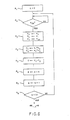
circuit 16 can also be realized by a combination of a processor 31 for executing calculation of P, a read only memory (ROM) 32 for memorizing a program for the calculation and the weight coefficients gi, and a random access memory (RAM) 33 for storing the series of sampled and equalized signals x(t). - Now, additionally referring to Fig. 6, operation will be described for calculating M·P1,2 similar to that calculated by the calculating circuit of Fig. 4.
- The processor 31 places m = 0 at an initial step S1 according to the program memorized in
ROM 32 and checks whether or not a signal is x(t) supplied as an input signal xin thereto from the line equalizer (15 in Fig. 3). When xin is supplied as a first one, the processor 31 stores xin as x₁ inRAM 33 as shown in step S3. Then, when next one of xin is supplied as second one, the processor 31 stores the second one of xin as x₁ inRAM 33 and rewrites the previous one of x₁ into x₂ at step S2. Thereafter, the processor 31 rewrites x₁, x₂, and x₃ into a current one of xin, a previous one of x₁, and a previous one of x₂, respectively, each supply of xin. In this connection, xin is supplied with a time interval of T as described above. Therefore, when m ≧ 3, x₂ = xk-1,τ and x₃ = xk-2,τ assuming that x₁ = xin is xk,τ. - Then, the processor 31 performs the calculations of c₁ = x₁·x₂ and C₂ = x₁·x₃ at step S4. It will be understood that C₁ and C₂ are corresponding to C₁(τ) and C₂(τ). At next step S5, weight coefficients gi for i = 1 and i = 2, that is, g1 = 1 and g2 = -1 and C = C₁ - C₂ is calculated. Then, the processor 31 executes a calculation of S = S + C at step S6 and adds 1 to m (m = m + 1). The processes from step S2 to step S7 are repeated for successive input signals xin and S is delivered from the processor 31 as MP1,2 when the m = M. Thereafter, the processor 31 places m = 0 and repeats the same processes.
- It will be readily understood by those skilled in the art that the calculating circuit of Fig. 5 can also be formed to calculate a linear summation of desired elements of the autocorrelation function Ci(τ) by modifying the program.
Claims (7)
calculating means coupled with said baud rate sampling circuit for calculating a linear summation of predetermined elements of an autocorrelation function of said series of sampled signals as a power of said series of sampled signals; and
sampling control means responsive to said power for controlling a sampling phase of said sampling signal so that said power is maximized.
Applications Claiming Priority (2)
| Application Number | Priority Date | Filing Date | Title |
|---|---|---|---|
| JP28894087 | 1987-11-16 | ||
| JP288940/87 | 1987-11-16 |
Publications (3)
| Publication Number | Publication Date |
|---|---|
| EP0316876A2 true EP0316876A2 (en) | 1989-05-24 |
| EP0316876A3 EP0316876A3 (en) | 1991-05-08 |
| EP0316876B1 EP0316876B1 (en) | 1994-01-26 |
Family
ID=17736778
Family Applications (1)
| Application Number | Title | Priority Date | Filing Date |
|---|---|---|---|
| EP88119033A Expired - Lifetime EP0316876B1 (en) | 1987-11-16 | 1988-11-15 | A digital signal receiving circuit with means for controlling a baud rate sampling phase by a power of sampled signals |
Country Status (5)
| Country | Link |
|---|---|
| US (1) | US5048060A (en) |
| EP (1) | EP0316876B1 (en) |
| AU (1) | AU610658B2 (en) |
| CA (1) | CA1305768C (en) |
| DE (1) | DE3887459T2 (en) |
Cited By (5)
| Publication number | Priority date | Publication date | Assignee | Title |
|---|---|---|---|---|
| US5128960A (en) * | 1990-09-06 | 1992-07-07 | Ncr Corporation | Clock recovery for a wireless local area network station |
| FR2679085A1 (en) * | 1991-07-02 | 1993-01-15 | Motorola Inc | SYSTEM AND METHOD FOR CALCULATING THE CHANNEL GAIN AND THE NOISE VARIANCE OF A COMMUNICATION CHANNEL. |
| EP0547960A1 (en) * | 1991-12-19 | 1993-06-23 | Institut Français du Pétrole | Method and apparatus for measuring successive amplitude levels of signals received over a communication path |
| FR2734107A1 (en) * | 1995-05-11 | 1996-11-15 | Motorola Inc | METHOD AND DEVICE FOR RECOVERING SYNCHRONIZATION CLOCK BY SYMBOLS FROM A SIGNAL HAVING HIGH FREQUENCY POSSIBILITIES |
| WO2000018059A1 (en) * | 1998-09-23 | 2000-03-30 | Infineon Technologies Ag | Device and method for regulating the sampling rate in a data transfer system |
Families Citing this family (49)
| Publication number | Priority date | Publication date | Assignee | Title |
|---|---|---|---|---|
| US5263026A (en) * | 1991-06-27 | 1993-11-16 | Hughes Aircraft Company | Maximum likelihood sequence estimation based equalization within a mobile digital cellular receiver |
| US5309483A (en) * | 1991-09-16 | 1994-05-03 | Motorola, Inc. | Data recovery device |
| US5353312A (en) * | 1991-12-27 | 1994-10-04 | At&T Bell Laboratories | Equalizer-based timing recovery |
| US5318533A (en) * | 1992-02-21 | 1994-06-07 | Scimed Life Systems, Inc. | Balloon catheter inflation device including apparatus for monitoring and wireless transmission of inflation data, and system |
| US5247544A (en) * | 1992-03-26 | 1993-09-21 | Motorola, Inc. | Phase adjustment method and apparatus for use in a clock recovery circuit |
| US5742189A (en) * | 1994-09-16 | 1998-04-21 | Kabushiki Kaisha Toshiba | Frequency conversion circuit and radio communication apparatus with the same |
| US5581585A (en) * | 1994-10-21 | 1996-12-03 | Level One Communications, Inc. | Phase-locked loop timing recovery circuit |
| US5802118A (en) * | 1996-07-29 | 1998-09-01 | Cirrus Logic, Inc. | Sub-sampled discrete time read channel for computer storage systems |
| DE19724027C2 (en) * | 1997-06-06 | 1999-09-30 | Siemens Ag | Method and arrangement for receiving data |
| US6266172B1 (en) * | 1997-11-06 | 2001-07-24 | Agere Systems Optoelectronics Guardian Corp. | Signal bit rate and performance measurement for optical channel signals |
| KR100525548B1 (en) * | 2000-12-29 | 2005-10-31 | 엘지전자 주식회사 | Baudrate Detection Circuit of Universal Asynchronous Receiver/Transmitter |
| EP1453238A1 (en) * | 2003-02-25 | 2004-09-01 | CoreOptics, Inc., c/o The Corporation Trust Center | Self-timing method for adjustment of a sampling phase in an oversampling receiver and circuit |
| US20040223568A1 (en) * | 2003-05-09 | 2004-11-11 | Ming-Kang Liu | Phase sampling determination system |
| US20040223567A1 (en) * | 2003-05-09 | 2004-11-11 | Ming-Kang Liu | Clock recovery system |
| WO2005122460A1 (en) * | 2004-06-04 | 2005-12-22 | Opelcomm, Inc. | Clock recovery system and phase sampling determination system |
| US7775966B2 (en) | 2005-02-24 | 2010-08-17 | Ethicon Endo-Surgery, Inc. | Non-invasive pressure measurement in a fluid adjustable restrictive device |
| US7699770B2 (en) | 2005-02-24 | 2010-04-20 | Ethicon Endo-Surgery, Inc. | Device for non-invasive measurement of fluid pressure in an adjustable restriction device |
| US8066629B2 (en) | 2005-02-24 | 2011-11-29 | Ethicon Endo-Surgery, Inc. | Apparatus for adjustment and sensing of gastric band pressure |
| US8016744B2 (en) | 2005-02-24 | 2011-09-13 | Ethicon Endo-Surgery, Inc. | External pressure-based gastric band adjustment system and method |
| US7775215B2 (en) | 2005-02-24 | 2010-08-17 | Ethicon Endo-Surgery, Inc. | System and method for determining implanted device positioning and obtaining pressure data |
| US7658196B2 (en) | 2005-02-24 | 2010-02-09 | Ethicon Endo-Surgery, Inc. | System and method for determining implanted device orientation |
| US7927270B2 (en) | 2005-02-24 | 2011-04-19 | Ethicon Endo-Surgery, Inc. | External mechanical pressure sensor for gastric band pressure measurements |
| US8152710B2 (en) | 2006-04-06 | 2012-04-10 | Ethicon Endo-Surgery, Inc. | Physiological parameter analysis for an implantable restriction device and a data logger |
| US8870742B2 (en) | 2006-04-06 | 2014-10-28 | Ethicon Endo-Surgery, Inc. | GUI for an implantable restriction device and a data logger |
| US8187163B2 (en) | 2007-12-10 | 2012-05-29 | Ethicon Endo-Surgery, Inc. | Methods for implanting a gastric restriction device |
| US8100870B2 (en) | 2007-12-14 | 2012-01-24 | Ethicon Endo-Surgery, Inc. | Adjustable height gastric restriction devices and methods |
| US8377079B2 (en) | 2007-12-27 | 2013-02-19 | Ethicon Endo-Surgery, Inc. | Constant force mechanisms for regulating restriction devices |
| US8142452B2 (en) | 2007-12-27 | 2012-03-27 | Ethicon Endo-Surgery, Inc. | Controlling pressure in adjustable restriction devices |
| US8591395B2 (en) | 2008-01-28 | 2013-11-26 | Ethicon Endo-Surgery, Inc. | Gastric restriction device data handling devices and methods |
| US8192350B2 (en) | 2008-01-28 | 2012-06-05 | Ethicon Endo-Surgery, Inc. | Methods and devices for measuring impedance in a gastric restriction system |
| US8337389B2 (en) | 2008-01-28 | 2012-12-25 | Ethicon Endo-Surgery, Inc. | Methods and devices for diagnosing performance of a gastric restriction system |
| US7844342B2 (en) | 2008-02-07 | 2010-11-30 | Ethicon Endo-Surgery, Inc. | Powering implantable restriction systems using light |
| US8221439B2 (en) | 2008-02-07 | 2012-07-17 | Ethicon Endo-Surgery, Inc. | Powering implantable restriction systems using kinetic motion |
| US8114345B2 (en) | 2008-02-08 | 2012-02-14 | Ethicon Endo-Surgery, Inc. | System and method of sterilizing an implantable medical device |
| US8591532B2 (en) | 2008-02-12 | 2013-11-26 | Ethicon Endo-Sugery, Inc. | Automatically adjusting band system |
| US8057492B2 (en) | 2008-02-12 | 2011-11-15 | Ethicon Endo-Surgery, Inc. | Automatically adjusting band system with MEMS pump |
| US8034065B2 (en) | 2008-02-26 | 2011-10-11 | Ethicon Endo-Surgery, Inc. | Controlling pressure in adjustable restriction devices |
| US8233995B2 (en) | 2008-03-06 | 2012-07-31 | Ethicon Endo-Surgery, Inc. | System and method of aligning an implantable antenna |
| US8187162B2 (en) | 2008-03-06 | 2012-05-29 | Ethicon Endo-Surgery, Inc. | Reorientation port |
| EP2223431A4 (en) * | 2008-08-15 | 2010-09-01 | Lsi Corp | Ram list-decoding of near codewords |
| CN102077173B (en) | 2009-04-21 | 2015-06-24 | 艾格瑞系统有限责任公司 | Error-floor mitigation of codes using write verification |
| EP2252003A1 (en) | 2009-05-12 | 2010-11-17 | CoreOptics Inc. | Phase detection method and phase detector |
| WO2011073974A1 (en) * | 2009-12-15 | 2011-06-23 | Multiphy Ltd. | Method and system for coherent equalization of chromatic dispersion of optical signals in a fiber |
| US8464142B2 (en) | 2010-04-23 | 2013-06-11 | Lsi Corporation | Error-correction decoder employing extrinsic message averaging |
| US8499226B2 (en) | 2010-06-29 | 2013-07-30 | Lsi Corporation | Multi-mode layered decoding |
| US8458555B2 (en) | 2010-06-30 | 2013-06-04 | Lsi Corporation | Breaking trapping sets using targeted bit adjustment |
| US8504900B2 (en) * | 2010-07-02 | 2013-08-06 | Lsi Corporation | On-line discovery and filtering of trapping sets |
| US8768990B2 (en) | 2011-11-11 | 2014-07-01 | Lsi Corporation | Reconfigurable cyclic shifter arrangement |
| RU2012146685A (en) | 2012-11-01 | 2014-05-10 | ЭлЭсАй Корпорейшн | DATABASE DETAILS DATABASE FOR DECODER BASED ON SPARED PARITY CONTROL |
Citations (2)
| Publication number | Priority date | Publication date | Assignee | Title |
|---|---|---|---|---|
| FR2493646A1 (en) * | 1980-10-31 | 1982-05-07 | Thomson Csf | Synchroniser for analogue modulation transmitted data - operates on digital information samples rectified analogue signals at rate varied according to summation of various sample group amplitudes |
| JPS60135A (en) * | 1983-06-16 | 1985-01-05 | Toshiba Corp | Sampling pulse generating circuit |
Family Cites Families (6)
| Publication number | Priority date | Publication date | Assignee | Title |
|---|---|---|---|---|
| FR2534426A1 (en) * | 1982-10-11 | 1984-04-13 | Trt Telecom Radio Electr | SELF-ADAPTIVE EQUALIZER FOR BASE BAND DATA SIGNAL |
| DE3335417A1 (en) * | 1983-09-29 | 1985-04-18 | Siemens AG, 1000 Berlin und 8000 München | RECEIVING DEVICE FOR A BITSERIAL, ASYNCHRONOUS TRANSMISSION RANGE FOR HIGH DATA RATES |
| US4815103A (en) * | 1987-10-29 | 1989-03-21 | American Telephone And Telegraph Company | Equalizer-based timing recovery |
| GB8800739D0 (en) * | 1988-01-13 | 1988-02-10 | Ncr Co | Multipoint modem system having fast synchronization |
| NL8800490A (en) * | 1988-02-26 | 1989-09-18 | At & T & Philips Telecomm | RECIPIENT OF A SYSTEM FOR TRANSMITTING DATA SYMBOLS WITH GIVEN BAUD SPEED. |
| US4856030A (en) * | 1988-07-20 | 1989-08-08 | Itt Defense Communications | Apparatus and methods of locking a receiving modem to a transmitting modem employing a burst signal |
-
1988
- 1988-11-15 CA CA000583093A patent/CA1305768C/en not_active Expired - Fee Related
- 1988-11-15 DE DE88119033T patent/DE3887459T2/en not_active Expired - Fee Related
- 1988-11-15 EP EP88119033A patent/EP0316876B1/en not_active Expired - Lifetime
- 1988-11-16 US US07/271,979 patent/US5048060A/en not_active Expired - Fee Related
- 1988-11-16 AU AU25612/88A patent/AU610658B2/en not_active Ceased
Patent Citations (2)
| Publication number | Priority date | Publication date | Assignee | Title |
|---|---|---|---|---|
| FR2493646A1 (en) * | 1980-10-31 | 1982-05-07 | Thomson Csf | Synchroniser for analogue modulation transmitted data - operates on digital information samples rectified analogue signals at rate varied according to summation of various sample group amplitudes |
| JPS60135A (en) * | 1983-06-16 | 1985-01-05 | Toshiba Corp | Sampling pulse generating circuit |
Non-Patent Citations (3)
| Title |
|---|
| IEEE JOURNAL ON SELECTED AREAS IN COMMUNICATIONS, vol. SAC-4, no. 8, November 1986, pages 1302-1311; C.-P.J. TZENG et al.: "Timing recovery in digital subscriber loops using baud-rate sampling" * |
| IEEE TRANSACTIONS ON COMMUNICATIONS, vol. COM-33, no. 6, June 1985, pages 558-568; O. AGAZZI et al.: "Timing recovery in digital subscriber loops" * |
| PATENT ABSTRACTS OF JAPAN, vol. 9, no. 110 (E-314)[1833], 15th May 1985; & JP-A-60 000 135 (TOSHIBA K.K.) 05-01-1985 * |
Cited By (8)
| Publication number | Priority date | Publication date | Assignee | Title |
|---|---|---|---|---|
| US5128960A (en) * | 1990-09-06 | 1992-07-07 | Ncr Corporation | Clock recovery for a wireless local area network station |
| FR2679085A1 (en) * | 1991-07-02 | 1993-01-15 | Motorola Inc | SYSTEM AND METHOD FOR CALCULATING THE CHANNEL GAIN AND THE NOISE VARIANCE OF A COMMUNICATION CHANNEL. |
| EP0547960A1 (en) * | 1991-12-19 | 1993-06-23 | Institut Français du Pétrole | Method and apparatus for measuring successive amplitude levels of signals received over a communication path |
| FR2685486A1 (en) * | 1991-12-19 | 1993-06-25 | Inst Francais Du Petrole | METHOD AND DEVICE FOR MEASURING SUCCESSIVE AMPLITUDE LEVELS OF SIGNALS RECEIVED ON A TRANSMISSION CHANNEL. |
| US5351271A (en) * | 1991-12-19 | 1994-09-27 | Institut Francais Du Petrole | Method and device for measuring the successive amplitude levels of signals received on a transmission channel |
| FR2734107A1 (en) * | 1995-05-11 | 1996-11-15 | Motorola Inc | METHOD AND DEVICE FOR RECOVERING SYNCHRONIZATION CLOCK BY SYMBOLS FROM A SIGNAL HAVING HIGH FREQUENCY POSSIBILITIES |
| WO2000018059A1 (en) * | 1998-09-23 | 2000-03-30 | Infineon Technologies Ag | Device and method for regulating the sampling rate in a data transfer system |
| US6714613B2 (en) | 1998-09-23 | 2004-03-30 | Infineon Technologies Ag | Apparatus and method for controlling the sampling clock in a data transmission system |
Also Published As
| Publication number | Publication date |
|---|---|
| DE3887459D1 (en) | 1994-03-10 |
| AU610658B2 (en) | 1991-05-23 |
| AU2561288A (en) | 1989-05-18 |
| EP0316876B1 (en) | 1994-01-26 |
| EP0316876A3 (en) | 1991-05-08 |
| DE3887459T2 (en) | 1994-05-11 |
| US5048060A (en) | 1991-09-10 |
| CA1305768C (en) | 1992-07-28 |
Similar Documents
| Publication | Publication Date | Title |
|---|---|---|
| EP0316876B1 (en) | A digital signal receiving circuit with means for controlling a baud rate sampling phase by a power of sampled signals | |
| US4789994A (en) | Adaptive equalizer using precursor error signal for convergence control | |
| US5285482A (en) | Timing recovery device for receiver installation using adaptive equalization and oversampling associated with differentially coherent demodulation | |
| AU662087B2 (en) | A method and an arrangement of estimating transmitted symbols at a receiver in digital signal transmission | |
| EP0300449B1 (en) | Digital automatic line equalizer with means for controlling tap gains of transversal filter on mean power of output from the filter | |
| US5790598A (en) | Block decision feedback equalizer | |
| EP0023056B1 (en) | Arrangement having a non-recursive filter | |
| EP0516133B1 (en) | Adaptive maximum likelihood sequence estimator using channel estimators of respective order of impulse response | |
| US4455661A (en) | Dual processor digital modem apparatus | |
| EP0426026A2 (en) | Equalizer | |
| US5369668A (en) | Fast response matched filter receiver with decision feedback equalizer | |
| US4146840A (en) | Technique for obtaining symbol timing for equalizer weights | |
| EP0599311A2 (en) | Clock recovery circuit | |
| EP0052362A1 (en) | Fast start-up system for transversal equalizers | |
| EP0216183A2 (en) | Decision feedback equalizer with a pattern detector | |
| JPH05183456A (en) | Control signal generator | |
| EP0567211A2 (en) | Adaptive receiver for multipath fading channels | |
| US6341298B1 (en) | Signal equalization | |
| EP0529585A2 (en) | Channel impulse response estimator for MLSE receiver for rapidly changing channels | |
| US5793820A (en) | Automatic adaptive filtering according to frequency modulation rate | |
| EP0260851B1 (en) | Data transmission system with correlation receiver | |
| US4438521A (en) | Automatically adaptive transversal filter | |
| US4145747A (en) | Method for establishing a tap coefficient of an adaptive automatic equalizer | |
| US4672637A (en) | Adaptive bit synchronizer | |
| US20020027953A1 (en) | Low-complexity blind equalizer |
Legal Events
| Date | Code | Title | Description |
|---|---|---|---|
| PUAI | Public reference made under article 153(3) epc to a published international application that has entered the european phase |
Free format text: ORIGINAL CODE: 0009012 |
|
| 17P | Request for examination filed |
Effective date: 19881115 |
|
| AK | Designated contracting states |
Kind code of ref document: A2 Designated state(s): DE FR GB |
|
| PUAL | Search report despatched |
Free format text: ORIGINAL CODE: 0009013 |
|
| AK | Designated contracting states |
Kind code of ref document: A3 Designated state(s): DE FR GB |
|
| 17Q | First examination report despatched |
Effective date: 19920904 |
|
| GRAA | (expected) grant |
Free format text: ORIGINAL CODE: 0009210 |
|
| AK | Designated contracting states |
Kind code of ref document: B1 Designated state(s): DE FR GB |
|
| REF | Corresponds to: |
Ref document number: 3887459 Country of ref document: DE Date of ref document: 19940310 |
|
| ET | Fr: translation filed | ||
| PG25 | Lapsed in a contracting state [announced via postgrant information from national office to epo] |
Ref country code: GB Effective date: 19941115 |
|
| PLBE | No opposition filed within time limit |
Free format text: ORIGINAL CODE: 0009261 |
|
| STAA | Information on the status of an ep patent application or granted ep patent |
Free format text: STATUS: NO OPPOSITION FILED WITHIN TIME LIMIT |
|
| 26N | No opposition filed | ||
| GBPC | Gb: european patent ceased through non-payment of renewal fee |
Effective date: 19941115 |
|
| PGFP | Annual fee paid to national office [announced via postgrant information from national office to epo] |
Ref country code: FR Payment date: 20021108 Year of fee payment: 15 |
|
| PGFP | Annual fee paid to national office [announced via postgrant information from national office to epo] |
Ref country code: DE Payment date: 20021121 Year of fee payment: 15 |
|
| PG25 | Lapsed in a contracting state [announced via postgrant information from national office to epo] |
Ref country code: DE Free format text: LAPSE BECAUSE OF NON-PAYMENT OF DUE FEES Effective date: 20040602 |
|
| PG25 | Lapsed in a contracting state [announced via postgrant information from national office to epo] |
Ref country code: FR Free format text: LAPSE BECAUSE OF NON-PAYMENT OF DUE FEES Effective date: 20040730 |
|
| REG | Reference to a national code |
Ref country code: FR Ref legal event code: ST |