EP0287274A2 - Semiconductor hybrid device - Google Patents
Semiconductor hybrid device Download PDFInfo
- Publication number
- EP0287274A2 EP0287274A2 EP88303112A EP88303112A EP0287274A2 EP 0287274 A2 EP0287274 A2 EP 0287274A2 EP 88303112 A EP88303112 A EP 88303112A EP 88303112 A EP88303112 A EP 88303112A EP 0287274 A2 EP0287274 A2 EP 0287274A2
- Authority
- EP
- European Patent Office
- Prior art keywords
- leads
- plane
- board
- offset
- hybrid device
- Prior art date
- Legal status (The legal status is an assumption and is not a legal conclusion. Google has not performed a legal analysis and makes no representation as to the accuracy of the status listed.)
- Withdrawn
Links
Images
Classifications
-
- H—ELECTRICITY
- H01—ELECTRIC ELEMENTS
- H01R—ELECTRICALLY-CONDUCTIVE CONNECTIONS; STRUCTURAL ASSOCIATIONS OF A PLURALITY OF MUTUALLY-INSULATED ELECTRICAL CONNECTING ELEMENTS; COUPLING DEVICES; CURRENT COLLECTORS
- H01R12/00—Structural associations of a plurality of mutually-insulated electrical connecting elements, specially adapted for printed circuits, e.g. printed circuit boards [PCB], flat or ribbon cables, or like generally planar structures, e.g. terminal strips, terminal blocks; Coupling devices specially adapted for printed circuits, flat or ribbon cables, or like generally planar structures; Terminals specially adapted for contact with, or insertion into, printed circuits, flat or ribbon cables, or like generally planar structures
- H01R12/50—Fixed connections
- H01R12/51—Fixed connections for rigid printed circuits or like structures
- H01R12/55—Fixed connections for rigid printed circuits or like structures characterised by the terminals
- H01R12/57—Fixed connections for rigid printed circuits or like structures characterised by the terminals surface mounting terminals
-
- H—ELECTRICITY
- H01—ELECTRIC ELEMENTS
- H01L—SEMICONDUCTOR DEVICES NOT COVERED BY CLASS H10
- H01L25/00—Assemblies consisting of a plurality of individual semiconductor or other solid state devices ; Multistep manufacturing processes thereof
- H01L25/16—Assemblies consisting of a plurality of individual semiconductor or other solid state devices ; Multistep manufacturing processes thereof the devices being of types provided for in two or more different main groups of groups H01L27/00 - H01L33/00, or in a single subclass of H10K, H10N, e.g. forming hybrid circuits
-
- H—ELECTRICITY
- H05—ELECTRIC TECHNIQUES NOT OTHERWISE PROVIDED FOR
- H05K—PRINTED CIRCUITS; CASINGS OR CONSTRUCTIONAL DETAILS OF ELECTRIC APPARATUS; MANUFACTURE OF ASSEMBLAGES OF ELECTRICAL COMPONENTS
- H05K1/00—Printed circuits
- H05K1/02—Details
- H05K1/14—Structural association of two or more printed circuits
- H05K1/141—One or more single auxiliary printed circuits mounted on a main printed circuit, e.g. modules, adapters
-
- H—ELECTRICITY
- H05—ELECTRIC TECHNIQUES NOT OTHERWISE PROVIDED FOR
- H05K—PRINTED CIRCUITS; CASINGS OR CONSTRUCTIONAL DETAILS OF ELECTRIC APPARATUS; MANUFACTURE OF ASSEMBLAGES OF ELECTRICAL COMPONENTS
- H05K3/00—Apparatus or processes for manufacturing printed circuits
- H05K3/36—Assembling printed circuits with other printed circuits
- H05K3/366—Assembling printed circuits with other printed circuits substantially perpendicularly to each other
-
- H—ELECTRICITY
- H01—ELECTRIC ELEMENTS
- H01L—SEMICONDUCTOR DEVICES NOT COVERED BY CLASS H10
- H01L2224/00—Indexing scheme for arrangements for connecting or disconnecting semiconductor or solid-state bodies and methods related thereto as covered by H01L24/00
- H01L2224/01—Means for bonding being attached to, or being formed on, the surface to be connected, e.g. chip-to-package, die-attach, "first-level" interconnects; Manufacturing methods related thereto
- H01L2224/42—Wire connectors; Manufacturing methods related thereto
- H01L2224/47—Structure, shape, material or disposition of the wire connectors after the connecting process
- H01L2224/48—Structure, shape, material or disposition of the wire connectors after the connecting process of an individual wire connector
- H01L2224/4805—Shape
- H01L2224/4809—Loop shape
- H01L2224/48091—Arched
-
- H—ELECTRICITY
- H01—ELECTRIC ELEMENTS
- H01L—SEMICONDUCTOR DEVICES NOT COVERED BY CLASS H10
- H01L2924/00—Indexing scheme for arrangements or methods for connecting or disconnecting semiconductor or solid-state bodies as covered by H01L24/00
- H01L2924/0001—Technical content checked by a classifier
- H01L2924/0002—Not covered by any one of groups H01L24/00, H01L24/00 and H01L2224/00
-
- H—ELECTRICITY
- H05—ELECTRIC TECHNIQUES NOT OTHERWISE PROVIDED FOR
- H05K—PRINTED CIRCUITS; CASINGS OR CONSTRUCTIONAL DETAILS OF ELECTRIC APPARATUS; MANUFACTURE OF ASSEMBLAGES OF ELECTRICAL COMPONENTS
- H05K1/00—Printed circuits
- H05K1/02—Details
- H05K1/0213—Electrical arrangements not otherwise provided for
- H05K1/0216—Reduction of cross-talk, noise or electromagnetic interference
- H05K1/023—Reduction of cross-talk, noise or electromagnetic interference using auxiliary mounted passive components or auxiliary substances
- H05K1/0231—Capacitors or dielectric substances
-
- H—ELECTRICITY
- H05—ELECTRIC TECHNIQUES NOT OTHERWISE PROVIDED FOR
- H05K—PRINTED CIRCUITS; CASINGS OR CONSTRUCTIONAL DETAILS OF ELECTRIC APPARATUS; MANUFACTURE OF ASSEMBLAGES OF ELECTRICAL COMPONENTS
- H05K1/00—Printed circuits
- H05K1/02—Details
- H05K1/03—Use of materials for the substrate
- H05K1/0306—Inorganic insulating substrates, e.g. ceramic, glass
-
- H—ELECTRICITY
- H05—ELECTRIC TECHNIQUES NOT OTHERWISE PROVIDED FOR
- H05K—PRINTED CIRCUITS; CASINGS OR CONSTRUCTIONAL DETAILS OF ELECTRIC APPARATUS; MANUFACTURE OF ASSEMBLAGES OF ELECTRICAL COMPONENTS
- H05K1/00—Printed circuits
- H05K1/16—Printed circuits incorporating printed electric components, e.g. printed resistor, capacitor, inductor
- H05K1/167—Printed circuits incorporating printed electric components, e.g. printed resistor, capacitor, inductor incorporating printed resistors
-
- H—ELECTRICITY
- H05—ELECTRIC TECHNIQUES NOT OTHERWISE PROVIDED FOR
- H05K—PRINTED CIRCUITS; CASINGS OR CONSTRUCTIONAL DETAILS OF ELECTRIC APPARATUS; MANUFACTURE OF ASSEMBLAGES OF ELECTRICAL COMPONENTS
- H05K2201/00—Indexing scheme relating to printed circuits covered by H05K1/00
- H05K2201/09—Shape and layout
- H05K2201/09209—Shape and layout details of conductors
- H05K2201/09654—Shape and layout details of conductors covering at least two types of conductors provided for in H05K2201/09218 - H05K2201/095
- H05K2201/09709—Staggered pads, lands or terminals; Parallel conductors in different planes
-
- H—ELECTRICITY
- H05—ELECTRIC TECHNIQUES NOT OTHERWISE PROVIDED FOR
- H05K—PRINTED CIRCUITS; CASINGS OR CONSTRUCTIONAL DETAILS OF ELECTRIC APPARATUS; MANUFACTURE OF ASSEMBLAGES OF ELECTRICAL COMPONENTS
- H05K2201/00—Indexing scheme relating to printed circuits covered by H05K1/00
- H05K2201/10—Details of components or other objects attached to or integrated in a printed circuit board
- H05K2201/10227—Other objects, e.g. metallic pieces
- H05K2201/10386—Clip leads; Terminals gripping the edge of a substrate
-
- H—ELECTRICITY
- H05—ELECTRIC TECHNIQUES NOT OTHERWISE PROVIDED FOR
- H05K—PRINTED CIRCUITS; CASINGS OR CONSTRUCTIONAL DETAILS OF ELECTRIC APPARATUS; MANUFACTURE OF ASSEMBLAGES OF ELECTRICAL COMPONENTS
- H05K3/00—Apparatus or processes for manufacturing printed circuits
- H05K3/30—Assembling printed circuits with electric components, e.g. with resistor
- H05K3/32—Assembling printed circuits with electric components, e.g. with resistor electrically connecting electric components or wires to printed circuits
- H05K3/34—Assembling printed circuits with electric components, e.g. with resistor electrically connecting electric components or wires to printed circuits by soldering
- H05K3/3447—Lead-in-hole components
Definitions
- This invention relates to a semiconductor hybrid device.
- the board has additionally to be capable of being reworked by hand during manufacture or later in order to permit a faulty component to be replaced in the event of a repair to the board being necessary.
- the present invention was devised to economise on the space needed to mount components on a board and to enable the cost of manufacture of the board to be reduced.
- a semiconductor hybrid device comprising a non-electrically conductive substrate body in the shape of a plane, which body on a first side carries a thick film resistor arrangement and on a second side supports a TTL logic device together with a capacitor, the device having a first set of connection leads which are located in a plane parallel to the plane of the body and a second set which are offset from said first set.
- one set of said connection leads lies in the plane of the substrate body.
- the leads may be arranged such that the offset leads are positioned alternatively with the leads of the other set along one side of the body.
- those components which are mounted on the substrate bofy such that they protrude a significant distance fromthe substrate surface are located on the same side of the substrate as that towards which the offset leads are directed.
- the resistor arrangement may comprise two or more resistors, one end of each resistor being connected to a common output connection lead.
- the invention further comprises a printed circuit board including the aforementioned semiconductor hybrid device.
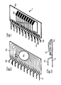
- the semiconductor hybrid device 1 has a substrate body 2 which is a small plate of a ceramic material.
- the body 2 carries on one side a thick film resistor arrangement 3 and on the opposite side a TTL logic device 4 and a capacitor 6.
- the substrate body 2 also supports a total of twenty connection leads and these leads are of two kinds, a straight lead 7 being alternated with an offset lead 8 along the length of one side of the body.
- the purpose of the offset shape of the leads 8 is to enable the leads to be suitably spaced from one another when they are connected to the metallised areas on a printed circuit board.
- the arrangement of the thick film resistors is one in which a number of resistor bodies is deposited on the surface of the body 2 with one end of each resistor being connected to a respective one of the connection leads 7, 8. The opposite end of every resistor is then connected to a common output lead and this common lead is joined to one of the connection leads 7, 8.
- the electrical terminals of the TTL logic device and the capacitor on the opposite side of the body 2 are similarly connected to respective ones of the connection leads 7, 8.
- the components which protrude a significant distance from the board surface are located on the same side of the board as that towards which the offset leads 8 are directed. This arrangement ensures tht the hybrid device will occupy only a minimum surface area when mounted on a printed circuit board.
- the substrate body 2 is given a coating 9 ( Figure 3) of an electrically insulating material to provide external protection.
- This coating 9 is a dip coating in a phenolic medium coloured black. It acts to protect the hybrid device from contamination or damage.
- connection leads 7, 8 are pushed through suitable holes in a printed circuit board and the board upper surface then comes to rest in a position close to a bend in the offset leads 8.
- the portions of the connection leads 7, 8 which protrude through the lower side of the board can then be soldered in place and any excess length of the leads can be removed in the usual way.
- the substrate body 2 is then seen to be maintained standing up in a plane normal to that of the board so that air is permitted to circulate freely round the hybrid device to allow effective cooling in operation.
- the device is able to occupy a much smaller area on the board than would be possible if it had been mounted in a plane parallel to the board plane.
- This area can be seen to be indeed rather small for a semiconductor device having twenty output leads and in a practical construction the dimensions of this area were 1.07 inches by 0.15 inches. This means that the device with its twenty leads was accommodated in an area of only 0.16 square inches on the board.
- One reason for attempting to pack more components on a board is to increase the performance of the board thereby improving the performance of equipment in which the board is to be used.
- a comparison of the areas (in square inches) occupied by the hybrid device of the invention and of Dual Inline and Leadless Devices is as follows: this device has had 0.1 inches added to each side to allow access to the board if necessary for rework apparatus.
- the dual inline and leadless devices require to have additional areas for a resistor pack and capacitor added to their basic board areas.
- the hybrid device of the invention already includes these components so the additions are not necessary.
- the construction of the present invention thus is accommodated in a package comprising logic device, capacitor and resistors and which occupies only a minimum part of the board area. This thus reduces the board area required to support these components and this can enable the overall cost of apparatus incorporating the semiconductor hybrid device to be reduced.
- the semiconductor hybrid device is also capable of being assembled on the board without the need for costly assembly equipment so this can lead to a further reduction in the overall cost of manufacturing the board.
- the substrate body was of a ceramic material but the use of this material is not essential. Alternative materials could be used that were electrically non-conductive and were sufficiently rigid to permit handling without damage to the components supported thereon.
Abstract
Description
- This invention relates to a semiconductor hybrid device.
- In the manufacture of electronic circuit boards, such as printed circuit boards, there is an ever increasing need to pack a greater number of components into a smaller area of the board. However, it is also required to facilitate the semi-automatic insertion of the components into the board so the components should not be too close together. The board has additionally to be capable of being reworked by hand during manufacture or later in order to permit a faulty component to be replaced in the event of a repair to the board being necessary.
- The present invention was devised to economise on the space needed to mount components on a board and to enable the cost of manufacture of the board to be reduced.
- According to the invention, there is provided a semiconductor hybrid device comprising a non-electrically conductive substrate body in the shape of a plane, which body on a first side carries a thick film resistor arrangement and on a second side supports a TTL logic device together with a capacitor, the device having a first set of connection leads which are located in a plane parallel to the plane of the body and a second set which are offset from said first set.
- Preferably, one set of said connection leads lies in the plane of the substrate body. The leads may be arranged such that the offset leads are positioned alternatively with the leads of the other set along one side of the body.
- In one embodiment, those components which are mounted on the substrate bofy such that they protrude a significant distance fromthe substrate surface, are located on the same side of the substrate as that towards which the offset leads are directed.
- The resistor arrangement may comprise two or more resistors, one end of each resistor being connected to a common output connection lead.
- The invention further comprises a printed circuit board including the aforementioned semiconductor hybrid device.
- By way of example, a particular embodiment of the invention will now be described with reference to the accompanying drawing, in which:
- Figure 1 and 2 are perspective views taken from both sides of the device, and,
- Figure 3 is a cross-sectional view taken just inside one end of the device.
- As depicted in Figures 1 and 2, the semiconductor hybrid device 1 has a
substrate body 2 which is a small plate of a ceramic material. Thebody 2 carries on one side a thickfilm resistor arrangement 3 and on the opposite side a TTL logic device 4 and acapacitor 6. - The
substrate body 2 also supports a total of twenty connection leads and these leads are of two kinds, astraight lead 7 being alternated with anoffset lead 8 along the length of one side of the body. The purpose of the offset shape of theleads 8 is to enable the leads to be suitably spaced from one another when they are connected to the metallised areas on a printed circuit board. - The arrangement of the thick film resistors is one in which a number of resistor bodies is deposited on the surface of the
body 2 with one end of each resistor being connected to a respective one of the connection leads 7, 8. The opposite end of every resistor is then connected to a common output lead and this common lead is joined to one of the connection leads 7, 8. By making electrical connections to a suitable pair of the connection leads 7, 8 a particular one of the resistor elements in the arrangement on thebody 2 can thus be selected. - The electrical terminals of the TTL logic device and the capacitor on the opposite side of the
body 2 are similarly connected to respective ones of the connection leads 7, 8. - It will be noticed that the components which protrude a significant distance from the board surface, are located on the same side of the board as that towards which the
offset leads 8 are directed. This arrangement ensures tht the hybrid device will occupy only a minimum surface area when mounted on a printed circuit board. - After the electrical connections have been made, the
substrate body 2 is given a coating 9 (Figure 3) of an electrically insulating material to provide external protection. This coating 9 is a dip coating in a phenolic medium coloured black. It acts to protect the hybrid device from contamination or damage. - In operation of the semiconductor hybrid device 1, the connection leads 7, 8 are pushed through suitable holes in a printed circuit board and the board upper surface then comes to rest in a position close to a bend in the offset leads 8. The portions of the connection leads 7, 8 which protrude through the lower side of the board can then be soldered in place and any excess length of the leads can be removed in the usual way.
- The
substrate body 2 is then seen to be maintained standing up in a plane normal to that of the board so that air is permitted to circulate freely round the hybrid device to allow effective cooling in operation. In addition, the device is able to occupy a much smaller area on the board than would be possible if it had been mounted in a plane parallel to the board plane. This area can be seen to be indeed rather small for a semiconductor device having twenty output leads and in a practical construction the dimensions of this area were 1.07 inches by 0.15 inches. This means that the device with its twenty leads was accommodated in an area of only 0.16 square inches on the board. - One reason for attempting to pack more components on a board is to increase the performance of the board thereby improving the performance of equipment in which the board is to be used.
- A comparison of the areas (in square inches) occupied by the hybrid device of the invention and of Dual Inline and Leadless Devices is as follows:


- The dual inline and leadless devices require to have additional areas for a resistor pack and capacitor added to their basic board areas. The hybrid device of the invention already includes these components so the additions are not necessary.
- If the average number of hybrid devices used on a board is ten, this can liberate a sufficient space on the board to allow twenty conventional components to be added to the board.
- The construction of the present invention thus is accommodated in a package comprising logic device, capacitor and resistors and which occupies only a minimum part of the board area. This thus reduces the board area required to support these components and this can enable the overall cost of apparatus incorporating the semiconductor hybrid device to be reduced. The semiconductor hybrid device is also capable of being assembled on the board without the need for costly assembly equipment so this can lead to a further reduction in the overall cost of manufacturing the board.
- The foregoing description of an embodiment of the invention has been given by way of example only and a number of modifications can be made without departing from the scope of the invention as defined in the appended claims. For instance, it is not essential that the device should accommodate only a single TTL logic device or a single capacitor. In different embodiments, more than one of these components could readily be incorporated.
- In the embodiment described, the substrate body was of a ceramic material but the use of this material is not essential. Alternative materials could be used that were electrically non-conductive and were sufficiently rigid to permit handling without damage to the components supported thereon.
Claims (8)
Applications Claiming Priority (2)
| Application Number | Priority Date | Filing Date | Title |
|---|---|---|---|
| GB08708904A GB2203591A (en) | 1987-04-14 | 1987-04-14 | Semiconductor hybrid device |
| GB8708904 | 1987-04-14 |
Publications (2)
| Publication Number | Publication Date |
|---|---|
| EP0287274A2 true EP0287274A2 (en) | 1988-10-19 |
| EP0287274A3 EP0287274A3 (en) | 1989-09-20 |
Family
ID=10615793
Family Applications (1)
| Application Number | Title | Priority Date | Filing Date |
|---|---|---|---|
| EP88303112A Withdrawn EP0287274A3 (en) | 1987-04-14 | 1988-04-07 | Semiconductor hybrid device |
Country Status (2)
| Country | Link |
|---|---|
| EP (1) | EP0287274A3 (en) |
| GB (1) | GB2203591A (en) |
Cited By (4)
| Publication number | Priority date | Publication date | Assignee | Title |
|---|---|---|---|---|
| EP0346035A2 (en) * | 1988-06-09 | 1989-12-13 | Oki Electric Industry Co., Ltd. | Terminal structure and process of fabricating the same |
| DE4444923A1 (en) * | 1993-12-21 | 1995-06-22 | Ibm | Printed circuit board with I / O connection areas on secondary areas |
| EP0804059A1 (en) * | 1996-04-23 | 1997-10-29 | Nec Corporation | Structure for mounting an electrical module on a board |
| US5973951A (en) * | 1992-05-19 | 1999-10-26 | Sun Microsystems, Inc. | Single in-line memory module |
Families Citing this family (1)
| Publication number | Priority date | Publication date | Assignee | Title |
|---|---|---|---|---|
| GB9320867D0 (en) * | 1993-10-11 | 1993-12-01 | Simpson Gareth | Adapter |
Citations (4)
| Publication number | Priority date | Publication date | Assignee | Title |
|---|---|---|---|---|
| EP0030335A2 (en) * | 1979-12-06 | 1981-06-17 | Siemens Aktiengesellschaft | Electroconductive board |
| DE3138285A1 (en) * | 1981-09-25 | 1983-04-07 | Siemens AG, 1000 Berlin und 8000 München | Supporting plate which can be plugged vertically onto a printed-circuit board by means of a plurality of rows of conductive pins, and a method for producing the supporting plate |
| EP0089248A2 (en) * | 1982-03-17 | 1983-09-21 | Fujitsu Limited | Dense mounting of semiconductor chip packages |
| JPS59224152A (en) * | 1983-06-03 | 1984-12-17 | Nec Ic Microcomput Syst Ltd | Integrated circuit device |
-
1987
- 1987-04-14 GB GB08708904A patent/GB2203591A/en active Pending
-
1988
- 1988-04-07 EP EP88303112A patent/EP0287274A3/en not_active Withdrawn
Patent Citations (4)
| Publication number | Priority date | Publication date | Assignee | Title |
|---|---|---|---|---|
| EP0030335A2 (en) * | 1979-12-06 | 1981-06-17 | Siemens Aktiengesellschaft | Electroconductive board |
| DE3138285A1 (en) * | 1981-09-25 | 1983-04-07 | Siemens AG, 1000 Berlin und 8000 München | Supporting plate which can be plugged vertically onto a printed-circuit board by means of a plurality of rows of conductive pins, and a method for producing the supporting plate |
| EP0089248A2 (en) * | 1982-03-17 | 1983-09-21 | Fujitsu Limited | Dense mounting of semiconductor chip packages |
| JPS59224152A (en) * | 1983-06-03 | 1984-12-17 | Nec Ic Microcomput Syst Ltd | Integrated circuit device |
Non-Patent Citations (1)
| Title |
|---|
| PATENT ABSTRACTS OF JAPAN, vol. 9, no. 99 (E-311)[1822], 27th April 1985; & JP-A-59 224 152 (NIHON DENKI AISHII MAIKON SYSTEM K.K.) 17-12-1984 * |
Cited By (8)
| Publication number | Priority date | Publication date | Assignee | Title |
|---|---|---|---|---|
| EP0346035A2 (en) * | 1988-06-09 | 1989-12-13 | Oki Electric Industry Co., Ltd. | Terminal structure and process of fabricating the same |
| EP0346035A3 (en) * | 1988-06-09 | 1991-01-16 | Oki Electric Industry Co., Ltd. | Terminal structure and process of fabricating the same |
| US4989318A (en) * | 1988-06-09 | 1991-02-05 | Oki Electric Industry Co., Ltd. | Process of assembling terminal structure |
| US5081764A (en) * | 1988-06-09 | 1992-01-21 | Oki Electric Industry Co., Ltd. | Terminal structure and process of fabricating the same |
| US5973951A (en) * | 1992-05-19 | 1999-10-26 | Sun Microsystems, Inc. | Single in-line memory module |
| DE4444923A1 (en) * | 1993-12-21 | 1995-06-22 | Ibm | Printed circuit board with I / O connection areas on secondary areas |
| EP0804059A1 (en) * | 1996-04-23 | 1997-10-29 | Nec Corporation | Structure for mounting an electrical module on a board |
| US5796592A (en) * | 1996-04-23 | 1998-08-18 | Nec Corporation | Module mounting structure |
Also Published As
| Publication number | Publication date |
|---|---|
| EP0287274A3 (en) | 1989-09-20 |
| GB8708904D0 (en) | 1987-05-20 |
| GB2203591A (en) | 1988-10-19 |
Similar Documents
| Publication | Publication Date | Title |
|---|---|---|
| US3912984A (en) | Auxiliary circuit package | |
| US3501582A (en) | Electrical assembly | |
| EP0065425B1 (en) | Hybrid integrated circuit component and printed circuit board mounting said component | |
| EP0000630B1 (en) | Microcircuit modules interconnector socket | |
| JPH0341752A (en) | Ic chip carrier package | |
| JP3043417B2 (en) | Electrical devices, for example switching and control devices for motor vehicles | |
| EP1107362B9 (en) | Electrical connection box | |
| US2885603A (en) | Pluggable circuit unit | |
| US3621112A (en) | Housing for electrical components | |
| US4272140A (en) | Arrangement for mounting dual-in-line packaged integrated circuits to thick/thin film circuits | |
| US5384433A (en) | Printed circuit structure including power, decoupling and signal termination | |
| EP0287274A2 (en) | Semiconductor hybrid device | |
| CA1140680A (en) | Electronic circuit arrangement mounted on printed circuit board | |
| US4883428A (en) | Test socket incorporating circuit elements | |
| US3719860A (en) | Circuit component mounting with cooling plate | |
| US3346773A (en) | Multilayer conductor board assembly | |
| GB2152753A (en) | Decoupling capacitor for integrated circuits and relationship with a printed circuit board | |
| US3522486A (en) | Control apparatus | |
| EP0071306A1 (en) | Electric coil | |
| JPH03196482A (en) | High-tension electrode | |
| US2990500A (en) | Electronic module | |
| JP2570336B2 (en) | Hybrid integrated circuit device | |
| US8094460B2 (en) | Orientation-tolerant land pattern and method of manufacturing the same | |
| US4933812A (en) | Package and circuit arrangement for housing and connecting polarized electrical components and method of manufacture | |
| US4389697A (en) | Circuit assembly having a component with leads extending therefrom and a connector both supported on a planar substrate |
Legal Events
| Date | Code | Title | Description |
|---|---|---|---|
| PUAI | Public reference made under article 153(3) epc to a published international application that has entered the european phase |
Free format text: ORIGINAL CODE: 0009012 |
|
| AK | Designated contracting states |
Kind code of ref document: A2 Designated state(s): AT BE CH DE ES FR GR IT LI LU NL SE |
|
| RAP1 | Party data changed (applicant data changed or rights of an application transferred) |
Owner name: RADSTONE TECHNOLOGY PLC |
|
| PUAL | Search report despatched |
Free format text: ORIGINAL CODE: 0009013 |
|
| AK | Designated contracting states |
Kind code of ref document: A3 Designated state(s): AT BE CH DE ES FR GR IT LI LU NL SE |
|
| STAA | Information on the status of an ep patent application or granted ep patent |
Free format text: STATUS: THE APPLICATION IS DEEMED TO BE WITHDRAWN |
|
| 18D | Application deemed to be withdrawn |
Effective date: 19900321 |