EP0283699A2 - Photoelectric conversion device - Google Patents
Photoelectric conversion device Download PDFInfo
- Publication number
- EP0283699A2 EP0283699A2 EP88101954A EP88101954A EP0283699A2 EP 0283699 A2 EP0283699 A2 EP 0283699A2 EP 88101954 A EP88101954 A EP 88101954A EP 88101954 A EP88101954 A EP 88101954A EP 0283699 A2 EP0283699 A2 EP 0283699A2
- Authority
- EP
- European Patent Office
- Prior art keywords
- layer
- photoelectric conversion
- conversion device
- electrode
- amorphous
- Prior art date
- Legal status (The legal status is an assumption and is not a legal conclusion. Google has not performed a legal analysis and makes no representation as to the accuracy of the status listed.)
- Granted
Links
- 238000006243 chemical reaction Methods 0.000 title claims abstract description 54
- 239000004065 semiconductor Substances 0.000 claims abstract description 65
- 230000005684 electric field Effects 0.000 claims abstract description 17
- 229910052736 halogen Inorganic materials 0.000 claims abstract description 15
- 150000002367 halogens Chemical class 0.000 claims abstract description 15
- 229910052739 hydrogen Inorganic materials 0.000 claims abstract description 15
- UFHFLCQGNIYNRP-UHFFFAOYSA-N Hydrogen Chemical compound [H][H] UFHFLCQGNIYNRP-UHFFFAOYSA-N 0.000 claims abstract description 14
- 239000001257 hydrogen Substances 0.000 claims abstract description 14
- 230000000903 blocking effect Effects 0.000 claims description 48
- 239000000758 substrate Substances 0.000 claims description 25
- HBMJWWWQQXIZIP-UHFFFAOYSA-N silicon carbide Chemical compound [Si+]#[C-] HBMJWWWQQXIZIP-UHFFFAOYSA-N 0.000 claims description 19
- 229910010271 silicon carbide Inorganic materials 0.000 claims description 18
- 229910052799 carbon Inorganic materials 0.000 claims description 11
- 239000000969 carrier Substances 0.000 claims description 11
- OKTJSMMVPCPJKN-UHFFFAOYSA-N Carbon Chemical group [C] OKTJSMMVPCPJKN-UHFFFAOYSA-N 0.000 claims description 10
- 229910052710 silicon Inorganic materials 0.000 claims description 8
- 239000000203 mixture Substances 0.000 claims description 6
- 239000010703 silicon Substances 0.000 claims description 6
- XUIMIQQOPSSXEZ-UHFFFAOYSA-N Silicon Chemical compound [Si] XUIMIQQOPSSXEZ-UHFFFAOYSA-N 0.000 claims description 4
- 239000013078 crystal Substances 0.000 claims description 4
- ZAMOUSCENKQFHK-UHFFFAOYSA-N Chlorine atom Chemical compound [Cl] ZAMOUSCENKQFHK-UHFFFAOYSA-N 0.000 claims description 2
- PXGOKWXKJXAPGV-UHFFFAOYSA-N Fluorine Chemical compound FF PXGOKWXKJXAPGV-UHFFFAOYSA-N 0.000 claims description 2
- ATJFFYVFTNAWJD-UHFFFAOYSA-N Tin Chemical compound [Sn] ATJFFYVFTNAWJD-UHFFFAOYSA-N 0.000 claims description 2
- 229910052801 chlorine Inorganic materials 0.000 claims description 2
- 239000000460 chlorine Substances 0.000 claims description 2
- 229910052731 fluorine Inorganic materials 0.000 claims description 2
- 239000011737 fluorine Substances 0.000 claims description 2
- 229910052732 germanium Inorganic materials 0.000 claims description 2
- GNPVGFCGXDBREM-UHFFFAOYSA-N germanium atom Chemical compound [Ge] GNPVGFCGXDBREM-UHFFFAOYSA-N 0.000 claims description 2
- 229910052718 tin Inorganic materials 0.000 claims description 2
- ZCYVEMRRCGMTRW-UHFFFAOYSA-N 7553-56-2 Chemical compound [I] ZCYVEMRRCGMTRW-UHFFFAOYSA-N 0.000 claims 1
- WKBOTKDWSSQWDR-UHFFFAOYSA-N Bromine atom Chemical compound [Br] WKBOTKDWSSQWDR-UHFFFAOYSA-N 0.000 claims 1
- GDTBXPJZTBHREO-UHFFFAOYSA-N bromine Substances BrBr GDTBXPJZTBHREO-UHFFFAOYSA-N 0.000 claims 1
- 229910052794 bromium Inorganic materials 0.000 claims 1
- 229910052740 iodine Inorganic materials 0.000 claims 1
- 239000011630 iodine Substances 0.000 claims 1
- 239000000463 material Substances 0.000 abstract description 19
- 230000035945 sensitivity Effects 0.000 abstract description 12
- 230000000694 effects Effects 0.000 abstract description 10
- 239000010410 layer Substances 0.000 description 149
- 229910021417 amorphous silicon Inorganic materials 0.000 description 24
- 239000007789 gas Substances 0.000 description 15
- 238000000034 method Methods 0.000 description 14
- 238000002347 injection Methods 0.000 description 12
- 239000007924 injection Substances 0.000 description 12
- 238000010276 construction Methods 0.000 description 11
- BLRPTPMANUNPDV-UHFFFAOYSA-N Silane Chemical compound [SiH4] BLRPTPMANUNPDV-UHFFFAOYSA-N 0.000 description 6
- 150000001875 compounds Chemical class 0.000 description 6
- 229910021419 crystalline silicon Inorganic materials 0.000 description 5
- 239000011521 glass Substances 0.000 description 5
- 229910052581 Si3N4 Inorganic materials 0.000 description 4
- 229910052782 aluminium Inorganic materials 0.000 description 4
- 239000002800 charge carrier Substances 0.000 description 4
- 238000005268 plasma chemical vapour deposition Methods 0.000 description 4
- HQVNEWCFYHHQES-UHFFFAOYSA-N silicon nitride Chemical compound N12[Si]34N5[Si]62N3[Si]51N64 HQVNEWCFYHHQES-UHFFFAOYSA-N 0.000 description 4
- 229910052785 arsenic Inorganic materials 0.000 description 3
- 229910052796 boron Inorganic materials 0.000 description 3
- 238000000151 deposition Methods 0.000 description 3
- HTXDPTMKBJXEOW-UHFFFAOYSA-N dioxoiridium Chemical compound O=[Ir]=O HTXDPTMKBJXEOW-UHFFFAOYSA-N 0.000 description 3
- PJXISJQVUVHSOJ-UHFFFAOYSA-N indium(III) oxide Inorganic materials [O-2].[O-2].[O-2].[In+3].[In+3] PJXISJQVUVHSOJ-UHFFFAOYSA-N 0.000 description 3
- 229910000457 iridium oxide Inorganic materials 0.000 description 3
- 229910052698 phosphorus Inorganic materials 0.000 description 3
- 239000012298 atmosphere Substances 0.000 description 2
- 230000001276 controlling effect Effects 0.000 description 2
- 238000003384 imaging method Methods 0.000 description 2
- 230000006698 induction Effects 0.000 description 2
- 239000007787 solid Substances 0.000 description 2
- 229910052959 stibnite Inorganic materials 0.000 description 2
- XOLBLPGZBRYERU-UHFFFAOYSA-N tin dioxide Chemical compound O=[Sn]=O XOLBLPGZBRYERU-UHFFFAOYSA-N 0.000 description 2
- 229910001887 tin oxide Inorganic materials 0.000 description 2
- 229910017000 As2Se3 Inorganic materials 0.000 description 1
- 229910006992 Si1-xCx Inorganic materials 0.000 description 1
- 229910004014 SiF4 Inorganic materials 0.000 description 1
- VYPSYNLAJGMNEJ-UHFFFAOYSA-N Silicium dioxide Chemical compound O=[Si]=O VYPSYNLAJGMNEJ-UHFFFAOYSA-N 0.000 description 1
- 229910017817 a-Ge Inorganic materials 0.000 description 1
- 229910017875 a-SiN Inorganic materials 0.000 description 1
- 230000003321 amplification Effects 0.000 description 1
- 229910052787 antimony Inorganic materials 0.000 description 1
- 229910052793 cadmium Inorganic materials 0.000 description 1
- CETPSERCERDGAM-UHFFFAOYSA-N ceric oxide Chemical compound O=[Ce]=O CETPSERCERDGAM-UHFFFAOYSA-N 0.000 description 1
- 229910000422 cerium(IV) oxide Inorganic materials 0.000 description 1
- 229910052804 chromium Inorganic materials 0.000 description 1
- 229940000425 combination drug Drugs 0.000 description 1
- 230000007423 decrease Effects 0.000 description 1
- 230000003247 decreasing effect Effects 0.000 description 1
- 230000007547 defect Effects 0.000 description 1
- 238000006073 displacement reaction Methods 0.000 description 1
- 238000010894 electron beam technology Methods 0.000 description 1
- QUZPNFFHZPRKJD-UHFFFAOYSA-N germane Chemical compound [GeH4] QUZPNFFHZPRKJD-UHFFFAOYSA-N 0.000 description 1
- 229910052986 germanium hydride Inorganic materials 0.000 description 1
- 229910003437 indium oxide Inorganic materials 0.000 description 1
- 229910052741 iridium Inorganic materials 0.000 description 1
- 238000004519 manufacturing process Methods 0.000 description 1
- 229910052758 niobium Inorganic materials 0.000 description 1
- 239000012299 nitrogen atmosphere Substances 0.000 description 1
- 238000003199 nucleic acid amplification method Methods 0.000 description 1
- 229910052958 orpiment Inorganic materials 0.000 description 1
- 238000001259 photo etching Methods 0.000 description 1
- 238000005546 reactive sputtering Methods 0.000 description 1
- 230000001105 regulatory effect Effects 0.000 description 1
- 229910052711 selenium Inorganic materials 0.000 description 1
- 238000000926 separation method Methods 0.000 description 1
- 229910052814 silicon oxide Inorganic materials 0.000 description 1
- ABTOQLMXBSRXSM-UHFFFAOYSA-N silicon tetrafluoride Chemical compound F[Si](F)(F)F ABTOQLMXBSRXSM-UHFFFAOYSA-N 0.000 description 1
- 239000002356 single layer Substances 0.000 description 1
- 238000004544 sputter deposition Methods 0.000 description 1
- 229910052715 tantalum Inorganic materials 0.000 description 1
- 229910052721 tungsten Inorganic materials 0.000 description 1
- 229910052725 zinc Inorganic materials 0.000 description 1
Images


Classifications
-
- H—ELECTRICITY
- H01—ELECTRIC ELEMENTS
- H01L—SEMICONDUCTOR DEVICES NOT COVERED BY CLASS H10
- H01L31/00—Semiconductor devices sensitive to infrared radiation, light, electromagnetic radiation of shorter wavelength or corpuscular radiation and specially adapted either for the conversion of the energy of such radiation into electrical energy or for the control of electrical energy by such radiation; Processes or apparatus specially adapted for the manufacture or treatment thereof or of parts thereof; Details thereof
- H01L31/08—Semiconductor devices sensitive to infrared radiation, light, electromagnetic radiation of shorter wavelength or corpuscular radiation and specially adapted either for the conversion of the energy of such radiation into electrical energy or for the control of electrical energy by such radiation; Processes or apparatus specially adapted for the manufacture or treatment thereof or of parts thereof; Details thereof in which radiation controls flow of current through the device, e.g. photoresistors
- H01L31/09—Devices sensitive to infrared, visible or ultraviolet radiation
- H01L31/095—Devices sensitive to infrared, visible or ultraviolet radiation comprising amorphous semiconductors
-
- H—ELECTRICITY
- H01—ELECTRIC ELEMENTS
- H01L—SEMICONDUCTOR DEVICES NOT COVERED BY CLASS H10
- H01L31/00—Semiconductor devices sensitive to infrared radiation, light, electromagnetic radiation of shorter wavelength or corpuscular radiation and specially adapted either for the conversion of the energy of such radiation into electrical energy or for the control of electrical energy by such radiation; Processes or apparatus specially adapted for the manufacture or treatment thereof or of parts thereof; Details thereof
- H01L31/0248—Semiconductor devices sensitive to infrared radiation, light, electromagnetic radiation of shorter wavelength or corpuscular radiation and specially adapted either for the conversion of the energy of such radiation into electrical energy or for the control of electrical energy by such radiation; Processes or apparatus specially adapted for the manufacture or treatment thereof or of parts thereof; Details thereof characterised by their semiconductor bodies
- H01L31/036—Semiconductor devices sensitive to infrared radiation, light, electromagnetic radiation of shorter wavelength or corpuscular radiation and specially adapted either for the conversion of the energy of such radiation into electrical energy or for the control of electrical energy by such radiation; Processes or apparatus specially adapted for the manufacture or treatment thereof or of parts thereof; Details thereof characterised by their semiconductor bodies characterised by their crystalline structure or particular orientation of the crystalline planes
- H01L31/0376—Semiconductor devices sensitive to infrared radiation, light, electromagnetic radiation of shorter wavelength or corpuscular radiation and specially adapted either for the conversion of the energy of such radiation into electrical energy or for the control of electrical energy by such radiation; Processes or apparatus specially adapted for the manufacture or treatment thereof or of parts thereof; Details thereof characterised by their semiconductor bodies characterised by their crystalline structure or particular orientation of the crystalline planes including amorphous semiconductors
- H01L31/03762—Semiconductor devices sensitive to infrared radiation, light, electromagnetic radiation of shorter wavelength or corpuscular radiation and specially adapted either for the conversion of the energy of such radiation into electrical energy or for the control of electrical energy by such radiation; Processes or apparatus specially adapted for the manufacture or treatment thereof or of parts thereof; Details thereof characterised by their semiconductor bodies characterised by their crystalline structure or particular orientation of the crystalline planes including amorphous semiconductors including only elements of Group IV of the Periodic System
- H01L31/03765—Semiconductor devices sensitive to infrared radiation, light, electromagnetic radiation of shorter wavelength or corpuscular radiation and specially adapted either for the conversion of the energy of such radiation into electrical energy or for the control of electrical energy by such radiation; Processes or apparatus specially adapted for the manufacture or treatment thereof or of parts thereof; Details thereof characterised by their semiconductor bodies characterised by their crystalline structure or particular orientation of the crystalline planes including amorphous semiconductors including only elements of Group IV of the Periodic System including AIVBIV compounds or alloys, e.g. SiGe, SiC
-
- H—ELECTRICITY
- H01—ELECTRIC ELEMENTS
- H01L—SEMICONDUCTOR DEVICES NOT COVERED BY CLASS H10
- H01L31/00—Semiconductor devices sensitive to infrared radiation, light, electromagnetic radiation of shorter wavelength or corpuscular radiation and specially adapted either for the conversion of the energy of such radiation into electrical energy or for the control of electrical energy by such radiation; Processes or apparatus specially adapted for the manufacture or treatment thereof or of parts thereof; Details thereof
- H01L31/08—Semiconductor devices sensitive to infrared radiation, light, electromagnetic radiation of shorter wavelength or corpuscular radiation and specially adapted either for the conversion of the energy of such radiation into electrical energy or for the control of electrical energy by such radiation; Processes or apparatus specially adapted for the manufacture or treatment thereof or of parts thereof; Details thereof in which radiation controls flow of current through the device, e.g. photoresistors
- H01L31/10—Semiconductor devices sensitive to infrared radiation, light, electromagnetic radiation of shorter wavelength or corpuscular radiation and specially adapted either for the conversion of the energy of such radiation into electrical energy or for the control of electrical energy by such radiation; Processes or apparatus specially adapted for the manufacture or treatment thereof or of parts thereof; Details thereof in which radiation controls flow of current through the device, e.g. photoresistors characterised by at least one potential-jump barrier or surface barrier, e.g. phototransistors
- H01L31/101—Devices sensitive to infrared, visible or ultraviolet radiation
- H01L31/102—Devices sensitive to infrared, visible or ultraviolet radiation characterised by only one potential barrier or surface barrier
- H01L31/107—Devices sensitive to infrared, visible or ultraviolet radiation characterised by only one potential barrier or surface barrier the potential barrier working in avalanche mode, e.g. avalanche photodiode
-
- H—ELECTRICITY
- H01—ELECTRIC ELEMENTS
- H01L—SEMICONDUCTOR DEVICES NOT COVERED BY CLASS H10
- H01L31/00—Semiconductor devices sensitive to infrared radiation, light, electromagnetic radiation of shorter wavelength or corpuscular radiation and specially adapted either for the conversion of the energy of such radiation into electrical energy or for the control of electrical energy by such radiation; Processes or apparatus specially adapted for the manufacture or treatment thereof or of parts thereof; Details thereof
- H01L31/18—Processes or apparatus specially adapted for the manufacture or treatment of these devices or of parts thereof
- H01L31/20—Processes or apparatus specially adapted for the manufacture or treatment of these devices or of parts thereof such devices or parts thereof comprising amorphous semiconductor materials
- H01L31/202—Processes or apparatus specially adapted for the manufacture or treatment of these devices or of parts thereof such devices or parts thereof comprising amorphous semiconductor materials including only elements of Group IV of the Periodic System
- H01L31/204—Processes or apparatus specially adapted for the manufacture or treatment of these devices or of parts thereof such devices or parts thereof comprising amorphous semiconductor materials including only elements of Group IV of the Periodic System including AIVBIV alloys, e.g. SiGe, SiC
-
- Y—GENERAL TAGGING OF NEW TECHNOLOGICAL DEVELOPMENTS; GENERAL TAGGING OF CROSS-SECTIONAL TECHNOLOGIES SPANNING OVER SEVERAL SECTIONS OF THE IPC; TECHNICAL SUBJECTS COVERED BY FORMER USPC CROSS-REFERENCE ART COLLECTIONS [XRACs] AND DIGESTS
- Y02—TECHNOLOGIES OR APPLICATIONS FOR MITIGATION OR ADAPTATION AGAINST CLIMATE CHANGE
- Y02E—REDUCTION OF GREENHOUSE GAS [GHG] EMISSIONS, RELATED TO ENERGY GENERATION, TRANSMISSION OR DISTRIBUTION
- Y02E10/00—Energy generation through renewable energy sources
- Y02E10/50—Photovoltaic [PV] energy
- Y02E10/548—Amorphous silicon PV cells
-
- Y—GENERAL TAGGING OF NEW TECHNOLOGICAL DEVELOPMENTS; GENERAL TAGGING OF CROSS-SECTIONAL TECHNOLOGIES SPANNING OVER SEVERAL SECTIONS OF THE IPC; TECHNICAL SUBJECTS COVERED BY FORMER USPC CROSS-REFERENCE ART COLLECTIONS [XRACs] AND DIGESTS
- Y02—TECHNOLOGIES OR APPLICATIONS FOR MITIGATION OR ADAPTATION AGAINST CLIMATE CHANGE
- Y02P—CLIMATE CHANGE MITIGATION TECHNOLOGIES IN THE PRODUCTION OR PROCESSING OF GOODS
- Y02P70/00—Climate change mitigation technologies in the production process for final industrial or consumer products
- Y02P70/50—Manufacturing or production processes characterised by the final manufactured product
Definitions
- This invention relates to a photoelectric conversion device for converting light into electric signal and in particular to a photoelectric conversion device having a high sensitivity, utilizing the charge multiplication effect.
- Such photoelectric conversion device includes e.g. a photocell, a one-dimensional image sensor, a two-dimensional image sensor, an image pick-up tube, etc.
- photoelectric conversion elements whose principal component is amorphous semiconductor
- a photocell a one-dimensional image sensor (e.g. JP-A-52-144992), a two-dimensional image sensor combining a solid state drive circuit with an amorphous semiconductor (e.g. JP-B-59-26154), a photoconductive image pick-up tube (e.g. JP-A-49-24619), etc.
- Some of these photoconversion devices adopt a blocking type structure having a junction characteristic of preventing charge injection from the signal electrodes to the photoconductive layer and some others adopt a structure, by which charge is injected from one or both of the electrodes, a so-called injection type structure.
- the blocking type structure having a characteristic of preventing charge injection from the exterior of the photoconductive layer since only the portion of the incident light, which is converted into electric charge within the photoconductive layer, generates a signal current, the gain of the photoelectric conversion is always smaller than 1.
- a device of blocking type structure can have a photoelectric conversion efficiency greater than 1, if a method is adopted, by which a blocking type structure is formed by an amorphous semiconductor layer, whose principal component is Se and in which avalanche multiplication is made to occur in order to amplify signals (U.S. Patent Application Serial No. 69159).
- the injection type structure is adopted for a photoelectric conversion device such as a photocell, a one-dimensional image sensor, a photoconductive layer piled-up type solid state photosensitive device, etc.
- a high sensitivity with a gain greater than 1 can be realized.
- this method by which a part of electric charge is injected in the interior of the sensor, the photoresponse is significantly deteriorated.
- the present inventors test-fabricated the structure stated above using amorphous Si, and confirmed that since local levels existing in the forbidden band were more numerous for amorphous Si than for crystalline Si, the depletion layer in the p-n junction portion did not satisfactorily extend, resulting in insufficient avalanche multiplication effect. Further, it was recognized that when the operating temperature exceeded the room temperature, dark current was increased, and it was not possible to apply an electric field thereon, which was so high that a sufficient avalanche multiplication effect could be obtained. These results indicate that there was a problem that no satisfactorily high amplification factor could be obtained only by forming an avalanche diode structure similar to that in crystalline Si by using amorphous Si.
- An object of this invetion is to provide a photoelectric conversion device having a good photoresponse, resolving the problematical points of the various techniques described previously.
- Another object of this invention is to provide a photoelectric conversion device made of amorphous semiconductor, which has a good heat-resisting property and whose photoelectric conversion efficiency is greater than 1.
- Still another object of this invention is to provide a photoelectric conversion device having low dark current.
- Still another object of this invention is to provide a photoelectric conversion device, for which a uniform photoelectric converting portion having a large area can be easily formed.
- Still another object of this invention is to provide a photoelectric conversion device, which can be fabricated by a simple process.
- a photoelectric conversion device is characterized in that it comprises a substrate; a first electrode formed on said substrate; a photoconductive layer for converting incident light into carriers, being formed on said first electrode, and having an amorphous semiconductor layer which is made mainly of at least one first element belonging to tetrahedral system and contains at least one second element selected from element group consisting of hydrogen and halogens; a means for applying electric field to said photoconductive layer, making said carriers run through said photoconductive layer and multiplying said carriers mainly in said amorphous semiconductor layer.
- the inventors of this invention had already discovered that a charge multiplication action takes place in an amorphous semiconductor layer made mainly of Se, when a strong electric field is applied to the amorphous semiconductor layer.
- a charge multiplication action takes place in an amorphous semiconductor layer made mainly of Se, when a strong electric field is applied to the amorphous semiconductor layer.
- the inventors have found that the material, in which the phenomena described above takes place, are not restricted to amorphous Se, but the blocking type junction can be formed by using a tetrahedral amorphous material stated above containing hydrogen or halogens and further that the charge multiplication action can be produced also mainly in the interior of a tetrahedral amorphous semiconductor layer just as in Se by adopting the blocking type structure described above and driving it while applying a high voltage to an inner region of the amorphous layer having no depletion region due to a junction, contrarily to the prior art method by which a p-n junction is formed in such an amorphous material and the avalanche multiplication is made to occur in the depletion region of the junction portion.
- carbon, silicon, germanium and tin can be used as an element of the tetrahedral system.
- this method by which the charge multiplication action is made to take place in an amorphous semiconductor layer while applying a strong electric field to the amorphous semiconductor layer, it is possible to obtain a photoelectric conversion device having a high sensitivity with a photoconductive gain greater than 1 without reducing the excellent photoresponse of the photosensitive element having the blocking type structure.
- the amorphous layer is about 0.5 to 10 ⁇ m thick.
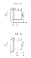
- Fig. 1A shows an example of the basic construction of a photoelectric conversion device for realizing this invention.
- the charge injection blocking layer 13 or 15 may be omitted, if a satisfactory rectifying contact can be obtained between the photoconductive layer 14 and the electrode 12 or the electrode 16.
- the amorphous semiconductor layer (although it is not shown in the figure, it must constitute at least a part of the photoconductive layer 14) is made of a material belonging to the tetrahedral system containing hydrogen or halogens and forms a blocking type structure, it is possible to apply a high electric field over the whole amorphous semiconductor layer and further to keep dark current at a value, which is smaller than 1/100 of that in a crystalline semiconductor, inspite of its large area.
- the thickness of the amorphous semiconductor layer and the direction of the electric field are so set that charge carriers having a larger ionization ratio between photogenerated electrons and holes for the adopted amorphous semiconductor body travel in the amorphous semiconductor layer under the high electric field so that the charge multiplication action is realized with a high efficiency, it is possible to obtain a device characteristic of operating stably with a high sensitivity with a photoconductive gain greater than 1 even for the temperatures higher than 80°C, maintaining the high speed photoresponse.
- amorphous semiconductor can be easily formed in a homogeneous and large thin layer and it is possible to deposit it on arbitrary substrate by a simple process. Consequently, from the view point that a uniform multiplication factor can be obtained, it can be understood that this invention is very useful.
- tetrahedral amorphous semiconductor material which is preferable for realizing this invention, compounds composed mainly of Si can be cited. These compounds have a feature that their forbidden band width can be varied by varying fabrication conditions or the composition ratio of Si and that they are excellent in the heat-resistive property.
- amorphous materials composed mainly of the compound of carbon and silicon (silicon carbide) containing hydrogen and/or halogens.
- the content of the added element of hydrogen or halogens is preferably 0.5 - 30 at.% and more preferably 5 - 20 at.%.
- This amorphous material is more excellent in the thermal stability with respect to Se and has in general a wider forbidden band and fewer thermally excited carriers with respect to amorphous Si. For these reasons, it has a smaller increase in dark current even at the high temperature operation.
- the forbidden band width can be easily varied by varying the composition ratio of carbon and silicon, it is possible to choose a material having the forbidden band width optimum for the utilization conditions and therefore the material is extremely useful. In this way, also with an amorphous semiconductor mainly composed of silicon carbide it is possible to resolve the problem at the high temperature operation, which is characteristic to a multiplication type imaging device using amorphous Se.
- the inventors of this invention have examined the avalanche multiplication in amorphous silicon carbide more in detail and found that amorphous silicon carbide with forbidden band width of 1.9 to 2.6 eV can be obtained for carbon composition ratio between 5 and 50%, and in such material, avalanche multiplication occurs efficiently, and that the thickness of the amorphous silicon carbide is preferably not less than 0.5 ⁇ m in order to obtain a satisfactory multiplication factor.
- V family such as P, As, etc. or elements of III family such as B, Al, etc.
- elements of V family such as P, As, etc. or elements of III family such as B, Al, etc.
- the amorphous silicon carbide layer is not necessarily simply a homogeneous layer, but a p-n junction may be formed therein, in order to have a structure, in which an avalanche multiplication can be produced efficiently in the junction portion, or the charge multiplication factor may be increased effectively by controlling the forbidden band width while varying the carbon concentration in the direction of the layer thickness.
- the electron injection blocking layer 15 amorphous silicon carbide or silicon nitride containing at least one of hydrogen and halogens, or p conductivity type amorphous silicon carbide or silicon nitride containing at least one of hydrogen and halogens and at least one of the elements of III family such as B, Al, etc., or oxide of Ir, or at least one of calcogenides such as Sb2S3, As2S3, As2Se3, Se-As-Te, etc., or a combination of more than 2 of the layers described above is suitable.
- the carbon composition ratio may be vary to a value greater than 50% depending on the sign of the carrier (i.e. electron or hole), whose injection should be blocked.
- the photoconductive layer may be constituted not by a single layer, but together with other thermally stable amorphous semiconductor layers overlaid thereon and having a similar charge multiplication action.
- the whole photoconductive layer is not necessarily amorphous semiconductor, but it may have a construction, in which a crystalline semiconductor layer such as Si, etc. and an amorphous semiconductor layer are overlaid on each other. Further, it may be so constructed that it is deposited on a substrate including signal reading-out circuits, etc.
- an amorphous semiconductor layer composed mainly of an element belonging to the tetrahedral system containing at least one of hydrogen and halogens as at least some of the layers constituting the photoconductive layer, and in which the charge multiplication is made to occur so as to enhance the sensitivity. Consequently, it is also possible that it is mainly the other layers in the photoconductive layer that have the function to absorb the incident light so as to produce photocarriers and that the amorphous semiconducting layer is used mainly for multiplying the carriers. In this case, there is a layer for generating photocarriers on the side, which is exposed to the incident light, in the photoconductive layer and the amorphous semiconductor layer may be made therebehind (in the direction of the propagation of the incident light).
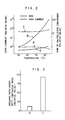
- Figs. 2 and 3 indicate effects obtained by realizing this invention.
- Fig. 2 indicates the temperature dependence of the dark current and the photoconductive gain when a photosensitive element (A) consisting of the transparent electrode 12, the hole blocking layer 13, the intrinsic amorphous silicon layer 14, the electron blocking layer 15 and the Al electrode 16 successively deposited on the transparent glass substrate 11, as indicated in Fig.
- A photosensitive element
- the photosensitive element (A) having an effective area of 1 cm2 and a photosensitive element (B), in which a p+ ⁇ p n junction is formed in amorphous silicon disposed on a transparent electrode deposited on a transparent substrate and further an Al electrode is deposited thereon, the photosensitive element (B) having an effective area of 1 cm2 are driven by applying such an electric field that an avalanche multiplication can occur in the whole amorphous silicon layer for the case (A) and in the depletion layer of the p-n junction for the case (B).
- the gain is insufficient in all the temperature region and the dark current increases significantly with increasing temperature, while both the gain and the dark current of the photosensitive element (A) have satisfactory behavior.
- Fig. 3 indicates the endurance of the element (A) described above and an element (C) driven continuously for 100 hours at 80°C, the element (C) consisting of a transparent electrode, a hole blocking layer, an amorphous Se layer and an Au electrode successively deposited on a transparent substrate and having an effective area of 1 cm2.
- the endurance of the element (A) is remarkably reduced with respect to that of the element (C).
- silicon carbide is used as the amorphous semiconductor, effects similar to those indicated in Figs. 2 and 3 can be obtained.
- the example 1 will be explained, referring to Fig. 1A.
- a transparent electrode 12 composed mainly of iridium oxide is formed on a transparent substrate 11.
- An a-Si:H having a layer thickness of 0.5-10 ⁇ m is formed thereon as a photoconductive layer 14 including amorphous semiconductor by the plasma CVD method by using SiH4 as source gas.
- an a-SiC:H having a layer thickness of 10 nm doped with P at 50 ppm is formed thereon as a hole blocking layer 13 by using SiH4 and C2H6 as source gases and PH3 as doping gas.
- a photoelectric conversion device is obtained by depositing an Al electrode 16 as a counter electrode further thereon.
- Figs. 4A and 4B indicate the construction of a one-dimensional image sensor, which is an embodiment of this invention.
- Fig. 4A is a plan view showing a part thereof and
- Fig. 4B is a cross-sectional view along the XX ⁇ line in Fig. 4A.
- a transparent conductive film composed mainly of iridium oxide is deposited on a transparent substrate 41. Then the conductive film is separated into a plurality of portions by the photoetching so as to form individual reading-out electrodes 46.
- An a-Si:H having a layer thickness of 0.5-10 ⁇ m is formed further thereon as a photoconductive layer 44 containing amorphous semiconductor by means of the same mask by sputtering an Si target, using a mixed gas of Ar and H2.
- a-SiC:H having a layer thickness of 10 nm, doped with P at 50 ppm is formed further thereon as a hole blocking layer 43 by means of the same mask by using SiH4 and C2H6 as source gases and PH3 as doping gas.
- Al is deposited further thereon as a common electrode 42 by means of a mask different from that described above.
- the reading-out electrodes 46 are connected to a scanning circuit disposed on the substrate by a method such as bonding, etc. so as to obtain a one-dimensional image-sensor.
- FIG. 5 shows the construction of an image pick-up tube, which is another embodiment of this invention.
- a transparent electrode 52 composed mainly of In2O3 is formed on a glass substrate 51.
- an a-Si:H having a layer thickness of 0.5-10 ⁇ m is deposited by the plasma CVD method by using SiH4 as source gas so as to obtain a photoconductive layer 54.
- Sb2S3 is deposited to a layer thickness of 100 nm as an electron blocking layer 55 in an Ar atmosphere of 13.3 Pa (10 ⁇ 1 Torr).
- a target portion 50 of an image pick-up tube can be obtained by those described above from 51 to 55.
- An image pick-up tube is obtained by mounting this target portion 50 in a glass tube 58 including a cathode and electron beam deflecting and focusing electrodes 59 and evacuating the glass tube 58.
- FIG. 5 An example, in which this invention is applied to an image pick-up tube, similarly to Example 3, is shown.
- Ge is used as the element belonging to tetrahedral system.
- a transparent electrode 52 composed mainly of In2O3 is formed on a glass substrate 51.
- an a-Ge:H having a layer thickness of 0.5-10 ⁇ m is formed by the plasma CVD method by using GeH4 as source gas so as to obtain a photoconductive layer 54.
- amorphous material composed of Se-As-Te is deposited to a layer thickness of 100 nm as an electron blocking layer 55 in an N2 atmosphere of 13.3 Pa (10 ⁇ 1 Torr).
- An image pick-up tube is obtained by using an image pick-up tube target portion 50 thus obtained in the same way as in Example 3.
- amorphous silicon carbide (a-Si 1-x C x :H) is formed by the plasma CVD method using SiH4, SiF4, etc. and CH4, C2H6, C2H4, etc. as source gases or by the reactive sputtering method of Si in a gaseous medium of H, Ar, CH4, etc.
- the concentration of carbon in the layer is controlled by regulating the flow rate of the source gas and the partial pressure of the gas of the atmosphere.
- an n conductivity type a-SiC:H is obtained by adding a gaseous compound of an element of V family such as P, As, Sb, etc. and an p conductivity type a-SiC:H is obtained by adding a gaseous compound of an element of III family such as B, Al, etc.
- a transparent electrode 16 composed mainly of iridium oxide is formed on a transparent substrate 11.
- An a-Si70C30:H having a layer thickness of 0.5-10 ⁇ m is formed thereon as a photoconductive layer 14 including amorphous semiconductor.
- An a-Si50C50:H doped with P at 50 ppm is formed further thereon to a thickness of 10 nm so as to form a hole blocking layer 13.
- a photoelectric conversion device is obtained by depositing an Al electrode further thereon as a counter electrode 12.
- Fig. 6 shows the schematical construction of a light sensitive element, which is an embodiment of this invention.
- This light sensitive element is formed by depositing successively a transparent electrode 62 composed mainly of indium oxide, an electron blocking layer 65, a photoconductive layer 64, a hole blocking layer 63 and an Au electrode 66 on a transparent substrate 61.
- the electron blocking layer 65 consists of 3 layers 651 made of a-Si60C40:H and 3 layers 652 made of a-Si70C30:H doped with B at 10 ppm overlaid alternately on each other, each of the layers being 5 nm thick.
- the photoelectric conversion layer 64 is a layer 2-8 ⁇ m thick and made of a-Si80C20:H doped with P at 50 ppm.
- the hole blocking layer 63 consists of 4 layers 631 made of a-Si70C30:H doped with As at 50 ppm and 4 layers 632 made of a-Si50C50:H overlaid alternately on each other, each of the layers being 2.5 nm thick.
- carrier blocking layer made of a-SiC:H is effective wide forbidden band width and effective p or n conductivity type, having good characteristics, an excellent carrier blocking power, if it consits of undoped a-SiC:H layers having a wide forbidden band and doped a-SiC:H layers having a narrow forbidden band.
- An electrode 12 composed mainly of Cr is formed on a semi-insulating semiconductor substrate 11.
- a-SiN:H is deposited thereon to a layer thickness of 10 nm as a hole blocking layer 13.
- a-Si80C20:H is deposited thereon to a layer thickness of 0.5-10 ⁇ m as a photoconductive layer 14.
- a thin layer made of silicon oxide is deposited thereon to a layer thickness of 8 nm as an electron blocking layer 15.
- a photoelectric conversion device can be obtained by forming a transparent electrode 16 composed mainly of tin oxide further thereon.
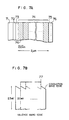
- Fig. 7A indicates a schematical construction of a light sensitive element, which is still another embodiment of this invention.
- the overall construction is identical to that indicated in Fig. 1B.
- This element consists of an electrode 72 composed mainly of Ta, a hole blocking layer 73, an amorphous semiconductor layer 74, an electron blocking layer 75, and a transparent electrode 76 successively formed on an arbitrary substrate 71.
- the hole blocking layer 73 is made of CeO2 having a layer thickness of 10 nm and the electron blocking layer 75 is made of a-Si70C30:H doped with B at 100 ppm and having a layer thickness of 10 nm.
- the amorphous semiconductor layer 74 is a layer 2 ⁇ m thick made of a-SiC:H.
- the amorphous semiconductor layer 74 is completed by repeating similar operations (by about 20 periods).
- the forbidden band width varies from 2.3 eV to 2.0 eV with a period of 100 nm.
- the forbidden band width varies significantly.
- the forbidden band width is varied by varying the composition of the compound consisting of Si and carbon as in this example, almost all the difference of the forbidden band width at the discontinuous portions 77 is attributable to displacement of the conduction band edge.
- traveling electrons gain energy corresponding to the energy difference of the conduction band edge, when they pass through the discontinuous portions 77 of the forbidden band width and thus it is possible to increase the effective electron multiplication factor with respect to that obtained in the case where the forbidden band width is continuous.
- An electrode 82 composed mainly of n+ conductivity type crystalline Si is formed on a semiinsulating semiconductor substrate 81.
- a hole blocking layer 83 made of a-Si70C30:H doped with P at 100 ppm is deposited thereon to a layer thickness of 5 nm.
- an amorphous semiconductor layer 84, 0.5-10 ⁇ m thick and composed mainly of a-SiC:H is formed further thereon.
- portions 842 where the forbidden band width is small are disposed within the amorphous semiconductor layer by controlling the C concentration in the layer.
- the C concentration in the layer is so controlled that it is 30 at.% in the first portion 841, 1.5 ⁇ m thick; it is decreased from 30 at.% to 0% in the succeeding portion 50 nm thick; it is constant at 0% in the succeeding portion 0.5 ⁇ m thick; and finally it is increased continuously from 0% to 30 at.% in the succeeding portion 50 nm thick.
- the forbidden band width is so shaped that it is 2.2 eV at the portion 841 where the C concentration is 30 at.% and 1.8 eV at the portion 842 where the C concentration is 0%, as shown in Fig. 8B. Therefore, the forbidden band width has a shape, as principally conduction band edge is narrowed.
- an electron blocking layer 85 10 nm thick and made of a-Si70C30:H doped with B at 100 ppm is formed further thereon.
- a transparent electrode 86 composed mainly of tin oxide is formed further thereon so as to obtain a photoelectric conversion device.
- the efficiency of the photoelectric conversion is increased especially for light having long wavelengths for adopting this structure so that the portion 842 having a narrow forbidden band width absorbs incident light with a high efficiency.
- the charge generation layer and the charge multiplication layer are substantially separated, it is possible to suppress noise generation accompanied by the charge multiplication.
Abstract
Description
- This invention relates to a photoelectric conversion device for converting light into electric signal and in particular to a photoelectric conversion device having a high sensitivity, utilizing the charge multiplication effect. Such photoelectric conversion device includes e.g. a photocell, a one-dimensional image sensor, a two-dimensional image sensor, an image pick-up tube, etc.
- Heretofore, as photoelectric conversion elements, whose principal component is amorphous semiconductor, there are known a photocell, a one-dimensional image sensor (e.g. JP-A-52-144992), a two-dimensional image sensor combining a solid state drive circuit with an amorphous semiconductor (e.g. JP-B-59-26154), a photoconductive image pick-up tube (e.g. JP-A-49-24619), etc. Some of these photoconversion devices adopt a blocking type structure having a junction characteristic of preventing charge injection from the signal electrodes to the photoconductive layer and some others adopt a structure, by which charge is injected from one or both of the electrodes, a so-called injection type structure.
- In an injection type element, since it is inherently possible to take-out charge carriers which are larger in number than the incident photons, a high sensitivity with a gain greater than 1 can be realized. In order to increase the sensitivity of the photoconversion element stated above, an imaging device has been proposed, in which a reading-out circuit and a photoconductive layer having e.g. phototransistor characteristics are overlaid upon each other (JP-A-61-222383).
- In order to achieve a similar object, a method utilizing an electrostatic induction type transistor as a device having a multiplication effect in its photoelectric converting portion itself has been proposed (IEEE Transactions on Electron Devices, Vol. ED 22, (1975) pages 185 - 197). There has been proposed also a method, by which a p⁺ π p n n⁺ structure is formed using an amorphous semiconductor, whose principal component is Si containing hydrogen and/or halogen (e.g. fluorine, chlorine, etc.), which structure is similar to that formed using crystalline Si, in which avalanche multiplication takes place in the depletion layer of its p-n junction portion in order to amplify signals. On the other hand, in the case where the blocking type structure having a characteristic of preventing charge injection from the exterior of the photoconductive layer is adopted, since only the portion of the incident light, which is converted into electric charge within the photoconductive layer, generates a signal current, the gain of the photoelectric conversion is always smaller than 1. However, it has been proposed by the invertors of this application that even a device of blocking type structure can have a photoelectric conversion efficiency greater than 1, if a method is adopted, by which a blocking type structure is formed by an amorphous semiconductor layer, whose principal component is Se and in which avalanche multiplication is made to occur in order to amplify signals (U.S. Patent Application Serial No. 69159).
- As described above, when the injection type structure is adopted for a photoelectric conversion device such as a photocell, a one-dimensional image sensor, a photoconductive layer piled-up type solid state photosensitive device, etc., since it is inherently possible to take-out charge carriers larger in number than the incident photons, a high sensitivity with a gain greater than 1 can be realized. However, by this method, by which a part of electric charge is injected in the interior of the sensor, the photoresponse is significantly deteriorated.
- Further, in the case of the electrostatic induction type transistor, it was difficult to have uniform multiplication factors at a same value for different pixels, because an amplifying portion was integrated in each of the pixels.
- On the other hand, in the example in which an amorphous semiconductor is used, since it is possible to form a homogeneous layer at a relatively low temperature and in addition the layer has a high resistivity, advantages can be obtained that no complicated pixel separation process as for crystalline Si is needed to realize a high resolution characteristic. However, for a photosensitive element, to which the avalanche multiplication phenomena in amorphous semiconductor are applied, there still remain several problematical points.
- That is, by the method by which a p⁺ π p n n⁺ structure identical to that adopted for an avalanche diode made of a crystalline semiconductor is formed using amorphous Si in order to amplify signals, a signal light is projected through the p⁺ region in the π region, where it is absorbed and converted into electric charge, which is in turn led to the p-n junction portion, and the avalanche multiplication takes place in the depletion layer of the p-n junction portion. In order to cause the avalanche multiplication, it is necessary that electric charge travels over a distance longer than a certain value. The present inventors test-fabricated the structure stated above using amorphous Si, and confirmed that since local levels existing in the forbidden band were more numerous for amorphous Si than for crystalline Si, the depletion layer in the p-n junction portion did not satisfactorily extend, resulting in insufficient avalanche multiplication effect. Further, it was recognized that when the operating temperature exceeded the room temperature, dark current was increased, and it was not possible to apply an electric field thereon, which was so high that a sufficient avalanche multiplication effect could be obtained. These results indicate that there was a problem that no satisfactorily high amplification factor could be obtained only by forming an avalanche diode structure similar to that in crystalline Si by using amorphous Si.
- Furthermore, in the case of the avalanche multiplication method using amorphous Se having a blocking type junction, although a large multiplication factor and a good photoresponse can be obtained, because of restrictions due to the material itself, e.g. in a high temperature environment over 80°C, there is a fear that the layer is altered during use and in particular there is a problem that element characteristics are unsatisfactory at high temperature operation.
- An object of this invetion is to provide a photoelectric conversion device having a good photoresponse, resolving the problematical points of the various techniques described previously.
- Another object of this invention is to provide a photoelectric conversion device made of amorphous semiconductor, which has a good heat-resisting property and whose photoelectric conversion efficiency is greater than 1.
- Still another object of this invention is to provide a photoelectric conversion device having low dark current.
- Still another object of this invention is to provide a photoelectric conversion device, for which a uniform photoelectric converting portion having a large area can be easily formed.
- Still another object of this invention is to provide a photoelectric conversion device, which can be fabricated by a simple process.
- In order to achieve these objects a photoelectric conversion device according to this invention is characterized in that it comprises a substrate; a first electrode formed on said substrate; a photoconductive layer for converting incident light into carriers, being formed on said first electrode, and having an amorphous semiconductor layer which is made mainly of at least one first element belonging to tetrahedral system and contains at least one second element selected from element group consisting of hydrogen and halogens; a means for applying electric field to said photoconductive layer, making said carriers run through said photoconductive layer and multiplying said carriers mainly in said amorphous semiconductor layer.
- According to this invention it is possible to obtain a photoelectric conversion device having a high sensitivity with a photoconductive gain greater than 1 and good thermal stability without reducing the excellent photoresponse of a photosensitive element using a photoconductive layer of blocking type structure.
-
- Figs. 1A and 1B are schemes illustrating examples of the basic construction of this invention;
- Figs. 2 and 3 are graphs explaining characteristics and the breaking ratio, respectively, of a device according to this invention and another device;
- Figs. 4A and 4B are schemes for explaining the structure of a one-dimensional image sensor, which is an embodiment of the photoelectric conversion device according to this invention;
- Fig. 5 is a scheme for explaining the structure of a image pick-up tube, which is another embodiment of the photoelectric conversion device according to this invention;
- Fig. 6 is a scheme for explaining the structure of a photosensitive element, which is still another embodiment of the photoelectric conversion device according to this invention;
- Figs. 7A and 7B are schemes for explaining the structure of another photosensitive element, which is still another embodiment of the photoelectric conversion device according to this invention;
- Figs. 8A and 8B are schemes for explaining the structure of still another photosensitive element, which is still another embodiment of the photoelectric conversion device according to this invention.
- The inventors of this invention had already discovered that a charge multiplication action takes place in an amorphous semiconductor layer made mainly of Se, when a strong electric field is applied to the amorphous semiconductor layer. Heretofore, it is generally thought that such phenomena hardly occur in an amorphous semiconductor layer itself, because there are a number of internal defects in the layer, and it has been believed that the amorphous Se is an exceptional material.
- This time, the inventors have found that the material, in which the phenomena described above takes place, are not restricted to amorphous Se, but the blocking type junction can be formed by using a tetrahedral amorphous material stated above containing hydrogen or halogens and further that the charge multiplication action can be produced also mainly in the interior of a tetrahedral amorphous semiconductor layer just as in Se by adopting the blocking type structure described above and driving it while applying a high voltage to an inner region of the amorphous layer having no depletion region due to a junction, contrarily to the prior art method by which a p-n junction is formed in such an amorphous material and the avalanche multiplication is made to occur in the depletion region of the junction portion. As an element of the tetrahedral system, carbon, silicon, germanium and tin can be used. By using this method, by which the charge multiplication action is made to take place in an amorphous semiconductor layer while applying a strong electric field to the amorphous semiconductor layer, it is possible to obtain a photoelectric conversion device having a high sensitivity with a photoconductive gain greater than 1 without reducing the excellent photoresponse of the photosensitive element having the blocking type structure.
- As a result of examining these phenomena more in detail, it has been found that the characteristics are not deteriorated even for the temperatures higher than 80°C and that the stability at the high temperature operation is especially excellent, if a material having a forbidden band width greater than 1.85 eV is used as the tetrahedral amorphous semiconductor material forming the blocking type structure described above.
- Further, it has been found that a satisfactory multiplication factor can be obtained, if the amorphous layer is about 0.5 to 10 µm thick.
- Fig. 1A shows an example of the basic construction of a photoelectric conversion device for realizing this invention. A transparent substrate 11; a
transparent electrode 12, whose thickness is not greater than 300 nm; a chargeinjection blocking layer 15 about 5 to 500 nm thick; aphotoconductive layer 14 about 0.5 to 10 µm thick containing amorphous semiconductor having the charge multiplication effect; a chargeinjection blocking layer 13 about 5 to 500 nm thick, which blocks injection of charge carriers, whose polarity is opposite to that of those blocked by the chargeinjection blocking layer 15; acounter electrode 16 and apower source 18 are fundamental portions thereof. However, in this construction, the chargeinjection blocking layer photoconductive layer 14 and theelectrode 12 or theelectrode 16. - To the photoelectric conversion device having the construction indicated in Fig. 1A an electric field necessary for realizing the avalanche multiplication in the amorphous semiconductor layer is applied by the
power source 18. As the inventors of this invention have discovered, in a device according to this invention, in which the amorphous semiconductor layer (although it is not shown in the figure, it must constitute at least a part of the photoconductive layer 14) is made of a material belonging to the tetrahedral system containing hydrogen or halogens and forms a blocking type structure, it is possible to apply a high electric field over the whole amorphous semiconductor layer and further to keep dark current at a value, which is smaller than 1/100 of that in a crystalline semiconductor, inspite of its large area. - In this state, when it is irradiated with light on the
transparent electrode 12 side, incident light is absorbed within the amorphous semiconductor layer so as to generate electron-hole pairs, which travel in the directions determined by the polarity of the applied electric field, opposite to each other. Consequently, if the thickness of the amorphous semiconductor layer and the direction of the electric field are so set that charge carriers having a larger ionization ratio between photogenerated electrons and holes for the adopted amorphous semiconductor body travel in the amorphous semiconductor layer under the high electric field so that the charge multiplication action is realized with a high efficiency, it is possible to obtain a device characteristic of operating stably with a high sensitivity with a photoconductive gain greater than 1 even for the temperatures higher than 80°C, maintaining the high speed photoresponse. For example, in the construction in Fig. 1A, it is mainly electrons that travel through the photoconductive layer 14 (amorphous semiconductor layer). - Furthermore, amorphous semiconductor can be easily formed in a homogeneous and large thin layer and it is possible to deposit it on arbitrary substrate by a simple process. Consequently, from the view point that a uniform multiplication factor can be obtained, it can be understood that this invention is very useful.
- As the tetrahedral amorphous semiconductor material, which is preferable for realizing this invention, compounds composed mainly of Si can be cited. These compounds have a feature that their forbidden band width can be varied by varying fabrication conditions or the composition ratio of Si and that they are excellent in the heat-resistive property.
- Further, the charge multiplication phenomena are observed also in amorphous materials composed mainly of the compound of carbon and silicon (silicon carbide) containing hydrogen and/or halogens. The content of the added element of hydrogen or halogens is preferably 0.5 - 30 at.% and more preferably 5 - 20 at.%. This amorphous material is more excellent in the thermal stability with respect to Se and has in general a wider forbidden band and fewer thermally excited carriers with respect to amorphous Si. For these reasons, it has a smaller increase in dark current even at the high temperature operation. Further, with the material described above, since the forbidden band width can be easily varied by varying the composition ratio of carbon and silicon, it is possible to choose a material having the forbidden band width optimum for the utilization conditions and therefore the material is extremely useful. In this way, also with an amorphous semiconductor mainly composed of silicon carbide it is possible to resolve the problem at the high temperature operation, which is characteristic to a multiplication type imaging device using amorphous Se.
- The inventors of this invention have examined the avalanche multiplication in amorphous silicon carbide more in detail and found that amorphous silicon carbide with forbidden band width of 1.9 to 2.6 eV can be obtained for carbon composition ratio between 5 and 50%, and in such material, avalanche multiplication occurs efficiently, and that the thickness of the amorphous silicon carbide is preferably not less than 0.5 µm in order to obtain a satisfactory multiplication factor.
- Further, a small amount of elements of V family such as P, As, etc. or elements of III family such as B, Aℓ, etc. may be added to amorphous silicon carbide for obtaining an avalanche multiplication layer. But, in this case, it is desirable to keep the resistivity at the room temperature over 10¹⁰ Ωcm.
- Furthermore, the amorphous silicon carbide layer is not necessarily simply a homogeneous layer, but a p-n junction may be formed therein, in order to have a structure, in which an avalanche multiplication can be produced efficiently in the junction portion, or the charge multiplication factor may be increased effectively by controlling the forbidden band width while varying the carbon concentration in the direction of the layer thickness.
- By the way, in the structures indicated in Figs. 1A and 1B, in the case where the carrier blocking characteristic is intensified by disposing the blocking layers 13, 15, the layer described below is useful.
- That is, as the
hole blocking layer 13 amorphous silicon carbide or silicon nitride containing at least one of hydrogen and halogens, or n conductivity type amorphous silicon carbide or silicon nitride containing at least one of hydrogen and halogens and at least one of the elements of V family such as P, As, etc., or oxide of at least one of Ce, Ge, Zn, Cd, Aℓ, Si, Nb, Ta, Cr and W, or a combination of more than 2 of the layers described above is suitable. - Further, as the electron
injection blocking layer 15 amorphous silicon carbide or silicon nitride containing at least one of hydrogen and halogens, or p conductivity type amorphous silicon carbide or silicon nitride containing at least one of hydrogen and halogens and at least one of the elements of III family such as B, Aℓ, etc., or oxide of Ir, or at least one of calcogenides such as Sb₂S₃, As₂S₃, As₂Se₃, Se-As-Te, etc., or a combination of more than 2 of the layers described above is suitable. - Here, for the silicon carbide used as the carrier blocking layer, contrarily to the silicon carbide used as the charge multiplication layer, the carbon composition ratio may be vary to a value greater than 50% depending on the sign of the carrier (i.e. electron or hole), whose injection should be blocked.
- Although a photoelectric conversion device using the charge multiplication effect in a tetrahedral amorphous semiconductor layer has been described above, for an amorphous semiconductor, contrarily to a crystal, since it is possible to overlay arbitrary different materials upon one another, the photoconductive layer may be constituted not by a single layer, but together with other thermally stable amorphous semiconductor layers overlaid thereon and having a similar charge multiplication action. In addition, the whole photoconductive layer is not necessarily amorphous semiconductor, but it may have a construction, in which a crystalline semiconductor layer such as Si, etc. and an amorphous semiconductor layer are overlaid on each other. Further, it may be so constructed that it is deposited on a substrate including signal reading-out circuits, etc. What is essential to this invention is that there is disposed an amorphous semiconductor layer composed mainly of an element belonging to the tetrahedral system containing at least one of hydrogen and halogens as at least some of the layers constituting the photoconductive layer, and in which the charge multiplication is made to occur so as to enhance the sensitivity. Consequently, it is also possible that it is mainly the other layers in the photoconductive layer that have the function to absorb the incident light so as to produce photocarriers and that the amorphous semiconducting layer is used mainly for multiplying the carriers. In this case, there is a layer for generating photocarriers on the side, which is exposed to the incident light, in the photoconductive layer and the amorphous semiconductor layer may be made therebehind (in the direction of the propagation of the incident light).
- Figs. 2 and 3 indicate effects obtained by realizing this invention. Fig. 2 indicates the temperature dependence of the dark current and the photoconductive gain when a photosensitive element (A) consisting of the
transparent electrode 12, thehole blocking layer 13, the intrinsicamorphous silicon layer 14, theelectron blocking layer 15 and theAℓ electrode 16 successively deposited on the transparent glass substrate 11, as indicated in Fig. 1B, the photosensitive element (A) having an effective area of 1 cm², and a photosensitive element (B), in which a p⁺ π p n junction is formed in amorphous silicon disposed on a transparent electrode deposited on a transparent substrate and further an Aℓ electrode is deposited thereon, the photosensitive element (B) having an effective area of 1 cm² are driven by applying such an electric field that an avalanche multiplication can occur in the whole amorphous silicon layer for the case (A) and in the depletion layer of the p-n junction for the case (B). By the photosensitive element (B) the gain is insufficient in all the temperature region and the dark current increases significantly with increasing temperature, while both the gain and the dark current of the photosensitive element (A) have satisfactory behavior. - Fig. 3 indicates the endurance of the element (A) described above and an element (C) driven continuously for 100 hours at 80°C, the element (C) consisting of a transparent electrode, a hole blocking layer, an amorphous Se layer and an Au electrode successively deposited on a transparent substrate and having an effective area of 1 cm². The endurance of the element (A) is remarkably reduced with respect to that of the element (C). In the case where silicon carbide is used as the amorphous semiconductor, effects similar to those indicated in Figs. 2 and 3 can be obtained.
- Although, in the above, examples, in which the avalanche effect in a thermally stable tetrahedral amorphous semiconductor is applied mainly to a photoelectric conversion device, have been described, it is matter of course that this invention can be applied as well to more general amplifying elements and switching elements apart from photoelectric conversion devices.
- Hereinbelow, this invention will be explained more in detail by using examples.
- The example 1 will be explained, referring to Fig. 1A.
- A
transparent electrode 12 composed mainly of iridium oxide is formed on a transparent substrate 11. An a-Si:H having a layer thickness of 0.5-10 µm is formed thereon as aphotoconductive layer 14 including amorphous semiconductor by the plasma CVD method by using SiH₄ as source gas. Further an a-SiC:H having a layer thickness of 10 nm doped with P at 50 ppm is formed thereon as ahole blocking layer 13 by using SiH₄ and C₂H₆ as source gases and PH₃ as doping gas. A photoelectric conversion device is obtained by depositing anAℓ electrode 16 as a counter electrode further thereon. - Figs. 4A and 4B indicate the construction of a one-dimensional image sensor, which is an embodiment of this invention. Fig. 4A is a plan view showing a part thereof and Fig. 4B is a cross-sectional view along the XXʹ line in Fig. 4A.
- A transparent conductive film composed mainly of iridium oxide is deposited on a
transparent substrate 41. Then the conductive film is separated into a plurality of portions by the photoetching so as to form individual reading-outelectrodes 46. An a-SiC:H having a layer thickness of 10 nm, doped with B at 50 ppm, is formed thereon as anelectron blocking layer 45 by means of a mask by using SiH₄ and C₂H₆ as source gases and B₂H₆ as doping gas. An a-Si:H having a layer thickness of 0.5-10 µm is formed further thereon as aphotoconductive layer 44 containing amorphous semiconductor by means of the same mask by sputtering an Si target, using a mixed gas of Ar and H₂. An a-SiC:H having a layer thickness of 10 nm, doped with P at 50 ppm is formed further thereon as ahole blocking layer 43 by means of the same mask by using SiH₄ and C₂H₆ as source gases and PH₃ as doping gas. Aℓ is deposited further thereon as acommon electrode 42 by means of a mask different from that described above. Thereafter, the reading-outelectrodes 46 are connected to a scanning circuit disposed on the substrate by a method such as bonding, etc. so as to obtain a one-dimensional image-sensor. - In the case where an electric field higher than 5 × 10⁷ V/m is applied to the photoelectric conversion device of the example 1 or 2 so that the
transparent substrate 11, 41 side is negative with respect to thecounter electrode incident light 17, 47 is projected to thetransparent substrate 11, 41, a high sensitivity with a gain greater than 1 can be realized without impairing the photoresponse. Further, even in the case where it is driven continuously for a long time at 80°C, no variations in the characteristics are caused. - Fig. 5 shows the construction of an image pick-up tube, which is another embodiment of this invention. A transparent electrode 52 composed mainly of In₂O₃ is formed on a
glass substrate 51. An a-Si:H having a layer thickness of 10 nm, doped with P at 50 ppm, is formed thereon as a hole blocking layer 53 by using PH₄ as doping gas. Then an a-Si:H having a layer thickness of 0.5-10 µm is deposited by the plasma CVD method by using SiH₄ as source gas so as to obtain a photoconductive layer 54. Then Sb₂S₃ is deposited to a layer thickness of 100 nm as anelectron blocking layer 55 in an Ar atmosphere of 13.3 Pa (10⁻¹ Torr). Atarget portion 50 of an image pick-up tube can be obtained by those described above from 51 to 55. An image pick-up tube is obtained by mounting thistarget portion 50 in aglass tube 58 including a cathode and electron beam deflecting and focusingelectrodes 59 and evacuating theglass tube 58. - An example, in which this invention is applied to an image pick-up tube, similarly to Example 3, is shown. In this example also Ge is used as the element belonging to tetrahedral system. In Fig. 5, a transparent electrode 52 composed mainly of In₂O₃ is formed on a
glass substrate 51. An a-Si:H having a layer thickness of 10 nm, doped with P at 50 ppm, is formed thereon as a hole blocking layer 53 by using PH₄ as doping gas. Then an a-Ge:H having a layer thickness of 0.5-10 µm is formed by the plasma CVD method by using GeH₄ as source gas so as to obtain a photoconductive layer 54. Thereafter amorphous material composed of Se-As-Te is deposited to a layer thickness of 100 nm as anelectron blocking layer 55 in an N₂ atmosphere of 13.3 Pa (10⁻¹ Torr). An image pick-up tube is obtained by using an image pick-uptube target portion 50 thus obtained in the same way as in Example 3. - When an electric field higher than 8 × 10⁷ V/m is applied to the photoconductive layer in the image pick-up tube in Example 3 or 4 so that the transparent electrode 52 is positive, it is possible to realize a high sensitivity with a photoconductive gain greater than 1 without impairing the photoresponse. Further it can be confirmed that its operation is thermally stable. In the
figure reference numeral 19 indicates a load resistance. - Now, several examples will be explained, in the case where the photoconductive layer composed of amorphous silicon carbide is formed as the amorphous semiconductor layer for charge multiplication. In the following examples amorphous silicon carbide (a-Si1-xCx:H) is formed by the plasma CVD method using SiH₄, SiF₄, etc. and CH₄, C₂H₆, C₂H₄, etc. as source gases or by the reactive sputtering method of Si in a gaseous medium of H, Ar, CH₄, etc. At this time, the concentration of carbon in the layer is controlled by regulating the flow rate of the source gas and the partial pressure of the gas of the atmosphere. Further, in the method described above, an n conductivity type a-SiC:H is obtained by adding a gaseous compound of an element of V family such as P, As, Sb, etc. and an p conductivity type a-SiC:H is obtained by adding a gaseous compound of an element of III family such as B, Aℓ, etc.
- Explanation will be made, referring to Fig. 1A.
- A
transparent electrode 16 composed mainly of iridium oxide is formed on a transparent substrate 11. An a-Si₇₀C₃₀:H having a layer thickness of 0.5-10 µm is formed thereon as aphotoconductive layer 14 including amorphous semiconductor. An a-Si₅₀C₅₀:H doped with P at 50 ppm is formed further thereon to a thickness of 10 nm so as to form ahole blocking layer 13. A photoelectric conversion device is obtained by depositing an Aℓ electrode further thereon as acounter electrode 12. - Fig. 6 shows the schematical construction of a light sensitive element, which is an embodiment of this invention. This light sensitive element is formed by depositing successively a
transparent electrode 62 composed mainly of indium oxide, anelectron blocking layer 65, aphotoconductive layer 64, ahole blocking layer 63 and anAu electrode 66 on atransparent substrate 61. Theelectron blocking layer 65 consists of 3layers 651 made of a-Si₆₀C₄₀:H and 3layers 652 made of a-Si₇₀C₃₀:H doped with B at 10 ppm overlaid alternately on each other, each of the layers being 5 nm thick. Thephotoelectric conversion layer 64 is a layer 2-8 µm thick and made of a-Si₈₀C₂₀:H doped with P at 50 ppm. Thehole blocking layer 63 consists of 4layers 631 made of a-Si₇₀C₃₀:H doped with As at 50 ppm and 4layers 632 made of a-Si₅₀C₅₀:H overlaid alternately on each other, each of the layers being 2.5 nm thick. As described above, it is possible to obtain carrier blocking layer made of a-SiC:H, is effective wide forbidden band width and effective p or n conductivity type, having good characteristics, an excellent carrier blocking power, if it consits of undoped a-SiC:H layers having a wide forbidden band and doped a-SiC:H layers having a narrow forbidden band. - Explanation will be made, referring to Fig. 1B.
- An
electrode 12 composed mainly of Cr is formed on a semi-insulating semiconductor substrate 11. a-SiN:H is deposited thereon to a layer thickness of 10 nm as ahole blocking layer 13. Then a-Si₈₀C₂₀:H is deposited thereon to a layer thickness of 0.5-10 µm as aphotoconductive layer 14. Thereafter a thin layer made of silicon oxide is deposited thereon to a layer thickness of 8 nm as anelectron blocking layer 15. A photoelectric conversion device can be obtained by forming atransparent electrode 16 composed mainly of tin oxide further thereon. - Fig. 7A indicates a schematical construction of a light sensitive element, which is still another embodiment of this invention. The overall construction is identical to that indicated in Fig. 1B. This element consists of an electrode 72 composed mainly of Ta, a
hole blocking layer 73, anamorphous semiconductor layer 74, anelectron blocking layer 75, and atransparent electrode 76 successively formed on an arbitrary substrate 71. Thehole blocking layer 73 is made of CeO₂ having a layer thickness of 10 nm and theelectron blocking layer 75 is made of a-Si₇₀C₃₀:H doped with B at 100 ppm and having a layer thickness of 10 nm. Theamorphous semiconductor layer 74 is a layer 2 µm thick made of a-SiC:H. At this time thefirst portion 100 nm thick is so formed that the C concentration in the layer decreases from 35% to 10%. This operation being considered to be one period, theamorphous semiconductor layer 74 is completed by repeating similar operations (by about 20 periods). As a result, as indicated in Fig. 7B, the forbidden band width varies from 2.3 eV to 2.0 eV with a period of 100 nm. In this case, at thediscontinuous portions 77 of the forbidden band width its value varies significantly. However, if the forbidden band width is varied by varying the composition of the compound consisting of Si and carbon as in this example, almost all the difference of the forbidden band width at thediscontinuous portions 77 is attributable to displacement of the conduction band edge. Consequently, in the case where this element is used while applying a negative bias to thetransparent electrode 76, traveling electrons gain energy corresponding to the energy difference of the conduction band edge, when they pass through thediscontinuous portions 77 of the forbidden band width and thus it is possible to increase the effective electron multiplication factor with respect to that obtained in the case where the forbidden band width is continuous. - Explanation will be made by referring to Figs. 8A and 8B.
- An
electrode 82 composed mainly of n⁺ conductivity type crystalline Si is formed on asemiinsulating semiconductor substrate 81. Ahole blocking layer 83 made of a-Si₇₀C₃₀:H doped with P at 100 ppm is deposited thereon to a layer thickness of 5 nm. Then anamorphous semiconductor layer 84, 0.5-10 µm thick and composed mainly of a-SiC:H is formed further thereon. At thistime portions 842 where the forbidden band width is small are disposed within the amorphous semiconductor layer by controlling the C concentration in the layer. For example, the C concentration in the layer is so controlled that it is 30 at.% in thefirst portion 841, 1.5 µm thick; it is decreased from 30 at.% to 0% in the succeedingportion 50 nm thick; it is constant at 0% in the succeeding portion 0.5 µm thick; and finally it is increased continuously from 0% to 30 at.% in the succeedingportion 50 nm thick. As a result, the forbidden band width is so shaped that it is 2.2 eV at theportion 841 where the C concentration is 30 at.% and 1.8 eV at theportion 842 where the C concentration is 0%, as shown in Fig. 8B. Therefore, the forbidden band width has a shape, as principally conduction band edge is narrowed. After that, anelectron blocking layer 85, 10 nm thick and made of a-Si₇₀C₃₀:H doped with B at 100 ppm is formed further thereon. Atransparent electrode 86 composed mainly of tin oxide is formed further thereon so as to obtain a photoelectric conversion device. The efficiency of the photoelectric conversion is increased especially for light having long wavelengths for adopting this structure so that theportion 842 having a narrow forbidden band width absorbs incident light with a high efficiency. In addition, in this way, since the charge generation layer and the charge multiplication layer are substantially separated, it is possible to suppress noise generation accompanied by the charge multiplication. - When an electric field higher than 5 × 10⁷ V/m is applied to a photoelectric conversion device described in one of the Example 5 to 9, it is possible to realize a high sensitivity with a photoconductive gain greater than 1 without impairing the photoresponse. Further no variations in characteristics are caused, even if they are operated continuously for a long time at a temperature of 80°C.
Claims (16)
a substrate (11, 41, 51, 61, 71, 81);
a first electrode (12, 52, 62, 72, 82) or a second electrode (16, 46) formed on said substrate;
a photoconductive layer (14, 44, 54, 64, 74, 84) for converting incident light into carriers, being formed on said first electrode, and having an amorphous semiconductor layer which is made mainly of at least one first element belonging to tetrahedral system and contains at least one second element selected from the group consisting of hydrogen and halogens;
means (18, 18ʹ) for applying electric field to said photoconductive layer, making said carriers run through said photoconductive layer and multiplying said carriers mainly in said amorphous semiconductor layer.
a substrate (11, 41, 51, 61, 71, 81);
a first electrode (12, 52, 62, 72, 82) or a second electrode (16, 46) formed on said substrate;
a photoconductive layer (14, 44, 54, 64, 74, 84) for converting incident light into carriers, being formed on said first electrode, and having an amorphous semiconductor layer which is made mainly of silicon carbide and contains at least one second element selected from the group consisting of hydrogen and halogens;
means (18, 18ʹ) for applying electric field to said photoconductive layer, making said carriers run through said photoconductive layer and multiplying said carriers in said amorphous semiconductor layer.
Applications Claiming Priority (4)
| Application Number | Priority Date | Filing Date | Title |
|---|---|---|---|
| JP65634/87 | 1987-03-23 | ||
| JP65633/87 | 1987-03-23 | ||
| JP62065634A JPS63233574A (en) | 1987-03-23 | 1987-03-23 | Optoelectronic transducer |
| JP62065633A JPH088075B2 (en) | 1987-03-23 | 1987-03-23 | Photoelectric conversion device |
Publications (3)
| Publication Number | Publication Date |
|---|---|
| EP0283699A2 true EP0283699A2 (en) | 1988-09-28 |
| EP0283699A3 EP0283699A3 (en) | 1989-10-04 |
| EP0283699B1 EP0283699B1 (en) | 1994-06-15 |
Family
ID=26406770
Family Applications (1)
| Application Number | Title | Priority Date | Filing Date |
|---|---|---|---|
| EP88101954A Expired - Lifetime EP0283699B1 (en) | 1987-03-23 | 1988-02-10 | Photoelectric conversion device |
Country Status (3)
| Country | Link |
|---|---|
| US (1) | US4980736A (en) |
| EP (1) | EP0283699B1 (en) |
| DE (1) | DE3850157T2 (en) |
Cited By (2)
| Publication number | Priority date | Publication date | Assignee | Title |
|---|---|---|---|---|
| EP0255246A2 (en) * | 1986-07-04 | 1988-02-03 | Hitachi, Ltd. | Image pick-up tube |
| US5233265A (en) * | 1986-07-04 | 1993-08-03 | Hitachi, Ltd. | Photoconductive imaging apparatus |
Families Citing this family (10)
| Publication number | Priority date | Publication date | Assignee | Title |
|---|---|---|---|---|
| US5196702A (en) * | 1987-10-21 | 1993-03-23 | Hitachi, Ltd. | Photo-sensor and method for operating the same |
| US6127692A (en) * | 1989-08-04 | 2000-10-03 | Canon Kabushiki Kaisha | Photoelectric conversion apparatus |
| US5260560A (en) * | 1990-03-02 | 1993-11-09 | Canon Kabushiki Kaisha | Photoelectric transfer device |
| US6031250A (en) * | 1995-12-20 | 2000-02-29 | Advanced Technology Materials, Inc. | Integrated circuit devices and methods employing amorphous silicon carbide resistor materials |
| JP2001135851A (en) * | 1999-11-05 | 2001-05-18 | Minolta Co Ltd | Photoelectric conversion element and solid-state imaging device |
| US6586332B1 (en) * | 2001-10-16 | 2003-07-01 | Lsi Logic Corporation | Deep submicron silicide blocking |
| EP1506327A1 (en) * | 2002-05-23 | 2005-02-16 | Universit de Sherbrooke | Ceramic thin film on various substrates, and process for producing same |
| JP2005012049A (en) * | 2003-06-20 | 2005-01-13 | Shimadzu Corp | Radiation detector and radiation pickup device equipped therewith |
| JP2005019543A (en) * | 2003-06-24 | 2005-01-20 | Shimadzu Corp | Two-dimensional semiconductor detector and two-dimensional imaging apparatus |
| CN102945887B (en) * | 2012-12-07 | 2015-09-09 | 东莞市五峰科技有限公司 | A kind of photoconductive semiconductor switch structure |
Citations (7)
| Publication number | Priority date | Publication date | Assignee | Title |
|---|---|---|---|---|
| EP0039219A1 (en) * | 1980-04-25 | 1981-11-04 | Hitachi, Ltd. | Light sensitive screen and devices including the same |
| US4329699A (en) * | 1979-03-26 | 1982-05-11 | Matsushita Electric Industrial Co., Ltd. | Semiconductor device and method of manufacturing the same |
| US4524237A (en) * | 1984-02-08 | 1985-06-18 | The United States Of America As Represented By The Administrator Of The National Aeronautics And Space Administration | Increased voltage photovoltaic cell |
| EP0151754A2 (en) * | 1984-02-14 | 1985-08-21 | Energy Conversion Devices, Inc. | An improved method of making a photoconductive member |
| EP0192473A2 (en) * | 1985-02-19 | 1986-08-27 | Exxon Research And Engineering Company | Amorphous photoreceptor with high sensitivity to long wavelengths |
| EP0194329A1 (en) * | 1985-03-13 | 1986-09-17 | Kanegafuchi Chemical Industry Co., Ltd. | Multilayer photoconductive material |
| EP0276683A2 (en) * | 1987-01-14 | 1988-08-03 | Hitachi, Ltd. | Photoelectric conversion device |
Family Cites Families (25)
| Publication number | Priority date | Publication date | Assignee | Title |
|---|---|---|---|---|
| JPS5230091B2 (en) * | 1972-07-03 | 1977-08-05 | ||
| JPS52144992A (en) * | 1976-05-28 | 1977-12-02 | Hitachi Ltd | Light receiving element |
| US4109271A (en) * | 1977-05-27 | 1978-08-22 | Rca Corporation | Amorphous silicon-amorphous silicon carbide photovoltaic device |
| US4117506A (en) * | 1977-07-28 | 1978-09-26 | Rca Corporation | Amorphous silicon photovoltaic device having an insulating layer |
| FR2408915A1 (en) * | 1977-11-10 | 1979-06-08 | Thomson Csf | HETEROJUNCTION PHOTODIODE, OPERATING IN AVALANCHE UNDER LOW POLARIZATION VOLTAGE |
| US4258375A (en) * | 1979-04-09 | 1981-03-24 | Massachusetts Institute Of Technology | Gax In1-x Asy P1-y /InP Avalanche photodiode and method for its fabrication |
| US4490573A (en) * | 1979-12-26 | 1984-12-25 | Sera Solar Corporation | Solar cells |
| JPS5721876A (en) * | 1980-07-14 | 1982-02-04 | Canon Inc | Photosensor |
| JPS5793585A (en) * | 1980-12-02 | 1982-06-10 | Fujitsu Ltd | Semiconductor photoreceiving element |
| DE3280418T2 (en) * | 1981-07-17 | 1993-03-04 | Kanegafuchi Chemical Ind | AMORPHOUS SEMICONDUCTOR AND PHOTOVOLTAIC DEVICE MADE OF AMORPHOUS SILICON. |
| US4476477A (en) * | 1982-02-23 | 1984-10-09 | At&T Bell Laboratories | Graded bandgap multilayer avalanche photodetector with energy step backs |
| JPS58204527A (en) * | 1982-05-24 | 1983-11-29 | Semiconductor Energy Lab Co Ltd | Semiconductor with fiber structure and manufacture thereof |
| JPS5926154A (en) * | 1982-08-04 | 1984-02-10 | 日本セメント株式会社 | Crusher |
| JPS59108370A (en) * | 1982-12-14 | 1984-06-22 | Kanegafuchi Chem Ind Co Ltd | Photovoltaic device |
| JPH065765B2 (en) * | 1982-12-23 | 1994-01-19 | 株式会社半導体エネルギ−研究所 | Photoelectric conversion device |
| FR2545275B1 (en) * | 1983-04-27 | 1987-03-06 | Rca Corp | TANDEM PHOTODETECTOR |
| JPS59204283A (en) * | 1983-05-06 | 1984-11-19 | Agency Of Ind Science & Technol | Amorphous semiconductor photoconductive element |
| JPS59227168A (en) * | 1983-06-08 | 1984-12-20 | Fuji Electric Corp Res & Dev Ltd | Semiconductor radioactive ray detector |
| US4680607A (en) * | 1984-05-11 | 1987-07-14 | Sanyo Electric Co., Ltd. | Photovoltaic cell |
| JPS61222383A (en) * | 1985-03-28 | 1986-10-02 | Shizuoka Univ | Pickup device for amorphous semiconductor |
| FR2585183B1 (en) * | 1985-07-19 | 1987-10-09 | Thomson Csf | METHOD FOR MANUFACTURING A LIGHT IMAGE DETECTOR AND TWO-DIMENSIONAL MATRIX DETECTOR OBTAINED BY THIS METHOD |
| JPS6249672A (en) * | 1985-08-29 | 1987-03-04 | Sumitomo Electric Ind Ltd | Amorphous photovoltaic element |
| US4718947A (en) * | 1986-04-17 | 1988-01-12 | Solarex Corporation | Superlattice doped layers for amorphous silicon photovoltaic cells |
| FR2597662B1 (en) * | 1986-04-22 | 1988-06-17 | Thomson Csf | PIN PHOTODIODE MADE FROM AMORPHOUS SEMICONDUCTOR |
| US4761680A (en) * | 1986-09-29 | 1988-08-02 | General Electric Company | Photodetector |
-
1988
- 1988-02-10 DE DE3850157T patent/DE3850157T2/en not_active Expired - Lifetime
- 1988-02-10 EP EP88101954A patent/EP0283699B1/en not_active Expired - Lifetime
- 1988-02-16 US US07/155,809 patent/US4980736A/en not_active Expired - Lifetime
Patent Citations (7)
| Publication number | Priority date | Publication date | Assignee | Title |
|---|---|---|---|---|
| US4329699A (en) * | 1979-03-26 | 1982-05-11 | Matsushita Electric Industrial Co., Ltd. | Semiconductor device and method of manufacturing the same |
| EP0039219A1 (en) * | 1980-04-25 | 1981-11-04 | Hitachi, Ltd. | Light sensitive screen and devices including the same |
| US4524237A (en) * | 1984-02-08 | 1985-06-18 | The United States Of America As Represented By The Administrator Of The National Aeronautics And Space Administration | Increased voltage photovoltaic cell |
| EP0151754A2 (en) * | 1984-02-14 | 1985-08-21 | Energy Conversion Devices, Inc. | An improved method of making a photoconductive member |
| EP0192473A2 (en) * | 1985-02-19 | 1986-08-27 | Exxon Research And Engineering Company | Amorphous photoreceptor with high sensitivity to long wavelengths |
| EP0194329A1 (en) * | 1985-03-13 | 1986-09-17 | Kanegafuchi Chemical Industry Co., Ltd. | Multilayer photoconductive material |
| EP0276683A2 (en) * | 1987-01-14 | 1988-08-03 | Hitachi, Ltd. | Photoelectric conversion device |
Non-Patent Citations (1)
| Title |
|---|
| PATENT ABSTRACTS OF JAPAN, vol. 6, no. 87 (E-108)(965), 25 May 1982 ; & JP-A-5721876 * |
Cited By (5)
| Publication number | Priority date | Publication date | Assignee | Title |
|---|---|---|---|---|
| EP0255246A2 (en) * | 1986-07-04 | 1988-02-03 | Hitachi, Ltd. | Image pick-up tube |
| EP0255246A3 (en) * | 1986-07-04 | 1989-04-26 | Hitachi, Ltd. | Photoconductive device and method of operating the same |
| US4888521A (en) * | 1986-07-04 | 1989-12-19 | Hitachi Ltd. | Photoconductive device and method of operating the same |
| US4952839A (en) * | 1986-07-04 | 1990-08-28 | Hitachi, Ltd | Photoconductive device and method of operating the same |
| US5233265A (en) * | 1986-07-04 | 1993-08-03 | Hitachi, Ltd. | Photoconductive imaging apparatus |
Also Published As
| Publication number | Publication date |
|---|---|
| DE3850157T2 (en) | 1995-02-09 |
| EP0283699A3 (en) | 1989-10-04 |
| US4980736A (en) | 1990-12-25 |
| DE3850157D1 (en) | 1994-07-21 |
| EP0283699B1 (en) | 1994-06-15 |
Similar Documents
| Publication | Publication Date | Title |
|---|---|---|
| US4598305A (en) | Depletion mode thin film semiconductor photodetectors | |
| US5723877A (en) | Photoelectric conversion apparatus | |
| JPH07115184A (en) | Layer-built solid-state image pickup device and its manufacture | |
| EP0283699B1 (en) | Photoelectric conversion device | |
| US5101255A (en) | Amorphous photoelectric conversion device with avalanche | |
| US5233265A (en) | Photoconductive imaging apparatus | |
| JPH05211321A (en) | Avalanche photodiode and signal processing device using thereof | |
| US3743899A (en) | Radiation-sensitive semiconductor target for a camera tube | |
| JP3018976B2 (en) | Semiconductor light receiving element | |
| US5155351A (en) | Photoelectric transfer device | |
| KR910000904B1 (en) | Target of image pickup tube | |
| US4453184A (en) | Solid state imaging device | |
| EP0428050A1 (en) | Photosensor having an amorphous silicon photoabsorption layer | |
| US5414275A (en) | Photoelectric converting device and image processing apparatus utilizing the same | |
| EP0437633A1 (en) | Photo-electric converter | |
| US5869851A (en) | Photoelectric conversion device with graded band gap and carrier concentration | |
| EP0495414B1 (en) | Photoelectric converting device and image processing apparatus utilizing the same | |
| US5260560A (en) | Photoelectric transfer device | |
| EP0276683B1 (en) | Photoelectric conversion device | |
| JP2810525B2 (en) | Driving method of photoelectric conversion device | |
| Chikamura et al. | A high-sensitivity solid-state image sensor using a thin-film ZnSe-Zn 1-x Cd x Te heterojunction photosensor | |
| Kaneko et al. | Amorphous Si: H heterojunction photodiode and its application to a compact scanner | |
| JPS6341227B2 (en) | ||
| JPS63233574A (en) | Optoelectronic transducer | |
| JP2977164B2 (en) | Photoelectric conversion device |
Legal Events
| Date | Code | Title | Description |
|---|---|---|---|
| PUAI | Public reference made under article 153(3) epc to a published international application that has entered the european phase |
Free format text: ORIGINAL CODE: 0009012 |
|
| AK | Designated contracting states |
Kind code of ref document: A2 Designated state(s): DE FR |
|
| PUAL | Search report despatched |
Free format text: ORIGINAL CODE: 0009013 |
|
| AK | Designated contracting states |
Kind code of ref document: A3 Designated state(s): DE FR |
|
| 17P | Request for examination filed |
Effective date: 19900327 |
|
| 17Q | First examination report despatched |
Effective date: 19920406 |
|
| GRAA | (expected) grant |
Free format text: ORIGINAL CODE: 0009210 |
|
| AK | Designated contracting states |
Kind code of ref document: B1 Designated state(s): DE FR |
|
| REF | Corresponds to: |
Ref document number: 3850157 Country of ref document: DE Date of ref document: 19940721 |
|
| ET | Fr: translation filed | ||
| PLBE | No opposition filed within time limit |
Free format text: ORIGINAL CODE: 0009261 |
|
| STAA | Information on the status of an ep patent application or granted ep patent |
Free format text: STATUS: NO OPPOSITION FILED WITHIN TIME LIMIT |
|
| 26N | No opposition filed | ||
| PGFP | Annual fee paid to national office [announced via postgrant information from national office to epo] |
Ref country code: FR Payment date: 20061220 Year of fee payment: 20 |
|
| PGFP | Annual fee paid to national office [announced via postgrant information from national office to epo] |
Ref country code: DE Payment date: 20070412 Year of fee payment: 20 |