EP0269911A2 - A microsequencer circuit - Google Patents
A microsequencer circuit Download PDFInfo
- Publication number
- EP0269911A2 EP0269911A2 EP87116405A EP87116405A EP0269911A2 EP 0269911 A2 EP0269911 A2 EP 0269911A2 EP 87116405 A EP87116405 A EP 87116405A EP 87116405 A EP87116405 A EP 87116405A EP 0269911 A2 EP0269911 A2 EP 0269911A2
- Authority
- EP
- European Patent Office
- Prior art keywords
- subroutine
- address
- memory
- addressing
- counter
- Prior art date
- Legal status (The legal status is an assumption and is not a legal conclusion. Google has not performed a legal analysis and makes no representation as to the accuracy of the status listed.)
- Withdrawn
Links
Images
Classifications
-
- G—PHYSICS
- G06—COMPUTING; CALCULATING OR COUNTING
- G06F—ELECTRIC DIGITAL DATA PROCESSING
- G06F9/00—Arrangements for program control, e.g. control units
- G06F9/06—Arrangements for program control, e.g. control units using stored programs, i.e. using an internal store of processing equipment to receive or retain programs
- G06F9/22—Microcontrol or microprogram arrangements
- G06F9/26—Address formation of the next micro-instruction ; Microprogram storage or retrieval arrangements
- G06F9/262—Arrangements for next microinstruction selection
- G06F9/264—Microinstruction selection based on results of processing
Definitions
- This invention relates to a data processing system and more particularly to a microsequencer circuit used in a sequential type microprocessor for increasing the speed of microcode/control word access and generation.
- data processing systems generally comprise a central unit, a main memory and plurality of peripheral units connected to the central unit by means of a plurality of input/output channels for the exchange of information.
- the data processing system functions by processing data according to well defined program instructions.
- the central unit comprises a control unit and an operative unit.
- the program instructions are interpreted and executed by means of microprograms which are microinstruction sequences read from a control memory by the control unit, one microinstruction at a time. Through suitable decoding the microinstructions generate a set of elementary commands, or microcommands, which cause the operation of several logic networks of the central unit in the manner required by the several program instructions.
- control unit includes a program counter which enable the control unit to sequentially execute the program instructions.
- execution of a program instruction may cause an interruption in the sequential execution thereof in order to execute a subroutine. All of the information regarding the status of the interrupted process must be saved in order to resume such process once the subroutine has been executed.
- One known technique for solving this problem include a register file or RAM partition dedicated to a push-down stack function where each consecutive branched-from address is stored in a last in/first out order. This technique requires the skipping of machine cycles in order to access the register file or RAM partition.
- a first control store memory contains the primary microinstruction group
- a second control store memory contains a branched-to subroutine microinstruction group
- possibly a third control store memory contains tertiary branched-to subroutine microinstruction groups.
- a branched-from address must be stored prior to accessing the secondary or tertiary control store memories.
- machine cycles must be skipped in order to access the branched-from address in order to resume the execution of the primary microinstruction group.
- the microsequencer circuit includes a memory means for storing a plurality of instructions therein and a first means for sequentially addressing the instructions.
- a second means responsive to a subroutine being addressed by the first addressing means, sequentially addresses instructions associated with the addressed subroutine.
- a branched-from address is stored in the first addressing means and a first address of the subroutine is loaded in the second addressing means.
- An enabling means facilitates the sequential accessing of the instructions of the subroutine until the execution thereof is completed. Thereafter, the enabling means disables the second addressing means and then re-enables the first addressing means to continue to sequentially address instructions stored in the memory means.
- the microsequencer includes a first programmed logic means for generating a first address associated with an instruction.
- a first counter which receives an input from the first programmed logic means, combines with the first logic means to sequentially address microcode stored in a second programmed logic means. Microcode stored in the second logic means is then sequentially addressed until a subroutine call is encountered. Thereafter, the first counter is disabled and a second counter is enabled in combination with the first programmed logic means and the first counter to sequentially access microcode associated with the called subroutine. After the subroutine has been executed, the second counter is disabled and the first counter re-enabled so that the first programmed logic means and the first counter continued to sequen tially address the microcode associated with the instruction.
- a program counter 12 facilitates the sequential execution of a plurality of program instruction stored in a random access memory (RAM) 14.
- a primary microinstruction group which includes a plurality of microinstructions, is stored in a control store memory such as a read only memory (ROM) or a programmed logic array (PLA) 16.
- a micro subroutine group which includes a plurality of subroutines each containing a plurality of microinstructions associated with the respective subroutine, is stored in ROM 16.
- Each of the stored microinstructions includes a field of control bits which may be fully encoded, practically encoded or unencoded.
- each microin struction includes a sequence field which specifies whether a selected microinstruction is to be succeeded by the next microinstruction in sequence or is either a conditional branch instruction, jump to subroutine instruction or return from subroutine instruction.
- a selected program instruction is feed to an instruction register (IR) 18.
- An op code associated with the selected program instruction is then decoded by a decoder circuit 20 in order to generate a microaddress which is associated with the op code.
- the microaddress is then loaded into a first microprogram counter 22 which facilitates the sequential accessing of microinstructions stored in the ROM 16. Thereafter, the microaddress contained in the first microprogram counter 22 is fed to an address register (not shown) associated with the ROM 16.
- CSDR control store data register
- each of the microinstructions stored in the ROM 16 includes a plurality of fields. These fields are used to activate or enable a digital device to being controlled such as the instruction register 18, an instruction unit 26 and logic circuit 28.
- the first microprogram counter 22 is then incremented to address the next sequentially stored microinstruction.
- the CSDR 24 facilitates the disabling of the first microprogram counter 22, the enabling of the second microprogram counter 30 and a switching of the multiplexer 32 to the second microprogram counter.
- the microprogram counter 22 retains the last microaddress stored therein as a branched-from address.
- the branched-from address is associated with the microinstruction which called the subroutine.
- the instruction unit 26 facilitates the loading of an address associated with the first microinstruction of the subroutine into the second microprogram counter 30.
- the second microprogram counter 30 is incremented to facilitate sequential addressing of microinstructions associated with the subroutine being executed.
- the CSDR 24 facilitates the re-enabling of the first microprogram counter 22, the disabling of the second microprogram counter 30 and the switching of the multiplexer 32 to the first microprogram counter.
- the first microprogram counter 22 is then incremented so that the next program instruction is executed in a sequential orderly manner.
- a program instruction is loaded into the instruction register 18.
- the op code associated with this instruction is decoded by the decoder circuit 20 and a starting address is loaded into the first program counter 22 when the instruction unit 26 generates a "fetch load clock signal.”
- the starting address is then fed through multiplexer 22 to the ROM 16.
- the addressed microinstruction is loaded into the CSDR 24.
- a logic zero is fed to the logic circuit 28 over lines 34 and 36 which indicates that the microinstruction stored in CSDR does not have the format of a jump instruction or a subroutine call and a subroutine will not be executed, respectively.
- a jump logic circuit 38 then generates a logic zero on its output line 40.
- Lines 34, 36 and 40 are coupled to inputs of an AND gate 42 which facilitate the generation of a logic zero on output line 44.
- the logic zero appearing on output 44 is fed to an input of a D-type flip flop 46 through NOR gates 48 and 50.
- the microinstructions stored in the ROM 16 are then addressed sequentially by the microprogram counter 22 until a subroutine call or jump instruction is encounter or a microinstruction is encountered which represents an "end of operation" (ENDOP).
- a logic one is fed to the logic circuit 28 over each of the lines 34 and 36. Moreover, the jump logic circuit 38 generates a logic one on its output line 40. A logic one now appears on output line 44 which enables the second microprogram counter 30 to load an address appearing on lines 54 and 56. Additionally, the logic one appearing on line 44 is fed through NOR gates 48 and 50 to the input of flip flop 46. Flip flop 46 then generates a logic one on its output which disables the first microprogram counter 22 and enables the second microprogram counter 30.
- the second microprogram counter 30 then sequentially accesses microinstructions associated with subroutine until a microinstruction is accessed which represents a subroutine return. Thereafter, the CSDR 24 feeds a signal representing the subroutine return to an input of an AND gate 58 which causes a flip flop 46 to generate a logic zero on its output. The logic zero appearing on the output of the flip flop 46 facilitates the enabling and incrementing of the first microprogram counter 22 and the disabling of the second microprogram counter 30. Thus, the first microprogram counter 22 then proceeds to sequentially access microinstructions stored in the ROM 16 until the ENDOP statement or another subroutine call is encountered.
- the microinstruction loaded in the CSDR 24 may represent a conditional or unconditional jump instruction.
- the CSDR 24 then feeds a logic one over line 34 and logic zero over line 36 to the logic circuit 28.
- the CSDR 24 also feeds conditional jump signals to the jump logic circuit 38 over line 59.
- Line 34 is coupled to and feeds the logic one to inputs of AND gates 42, 60 and 62.
- the logic zero is feed to an input of AND gate 42 and through inverter 64 to an input of AND gate 62.
- the jump logic circuit 38 then generates a logic one on output line 40 if the jump instruction is an unconditional jump instruction or, if the jump instruction is conditional, when the desired condition generated by the processor has occurred.
- Output line 66 is coupled to and feeds the logic one to an input of AND gate 62 and OR gate 67.
- the AND gate 62 then generates a logic one on output line 68 which is then fed to a multiplexer 70.
- Multiplexer 70 in, response to the logic one appearing on output line 68, switches its input from position 0 to position 1.
- the CSDR 24 feeds a next instruction or a jump address to a second input of the multiplexer 70 over line 54 and 72.
- microprogram counter 22 is enabled to load the next address by the logic one appearing on the output line 66.
- Micro program counter 22 then sequentially accesses microinstructions stored in the ROM 16 beginning with the "next instruction or jump address.”
- the microsequencer circuit 10 may also include a plurality of microprogram counters 74 each having input coupled to respective outputs of a demultiplexer circuit 76.
- the plurality of microprogram counters 74 facilitates the nesting of subroutines. If the microsequencer circuit 10 is executing a first subroutine and a subroutine call to a second subroutine is encountered, a branched-from address is stored in the second microprogram counter 30 and a starting of address is loaded into a selected one of the plurality of microprogram counters 74 under the control of the logic circuit 28. The selected one of the plurality of microprogram counters 74 then sequentially addresses the instructions associated with the second subroutine.
- microprogram counter 30 Whenever the second subroutine has been executed, the logic circuit 28 then re-enables microprogram counter 30 to sequentially address the remaining instructions of the first subroutine.
- the number of subroutines which can be nested using this technique is limited to the number of microprogram counters included in the plurality of microprogram counters 74.
- FIG. 3 there is shown a alternate embodiment of a microsequencer circuit 80 which utilizes associative memory techniques to establish a starting address.
- the microsequencer circuit 80 includes two PLAs' 82 and 84.
- An op code which associated with a program instruction, is fed through a multiplexer/decoder circuit 86 to an input of PLA 82.
- PLA 82 then decodes the op code and generates a starting address.
- a predetermined number of bits of the starting address are fed directly to an input of PLA 84 over a bus 88.
- the remaining bits of the starting address which are loaded into a first microprogram counter 90, are also fed to a second input of PLA 84.
- PLA 82 serves as an associative memory element which specifies a first, of a sequence, of addresses for each program instruction and for each microbranch, microcall and microsubroutine set of microcodes stored in PLA 84.
- PLA 84 includes a series of sequences of microcode which execute or generate a control word for each of the program instructions, micro branches, microcalls and microsubroutines.
- the control words generated by the PLA 84 are sequentially loaded into a control store data register (CSDR) 92.
- Each of the control words includes a control field which facilitates the operation of the first microprogram counter 90 and a second microprogram counter 94.
- the PLA 82 designates the starting address in PLA 84 and the first microprogram counter 90 sequences or counts through the microinstructions associated with the selected op codes. If during the sequencing by the first microprogram counter 90, a microsubroutine is encountered, the first microprogram counter is disabled and the second second microprogram counter is reset, loaded with a branch/next address stored in the CSDR 92 and enabled to sequence through the microinstructions of the microsubroutine.
- the address of the microsubroutine is a combination of the address appearing on bus 88, the contents of a first microprogram counter 90 and the contents of a second microprogram counter 94.
- This technique results in a control word have a fewer number of bits. For purposes of the illustration and not of limitation, let us assume that it takes ten bits to address PLA 84 additionally, assume that four bits of the starting address are placed on bus 88 by PLA 82, the first microprogram counter 90 is three bits wide and the second program counter 94 is three bits wide. In this manner, the next address field of the control word is required to be only three bits wide. The remainder of the address bits are generated by the PLA 82.
Abstract
Description
- This invention relates to a data processing system and more particularly to a microsequencer circuit used in a sequential type microprocessor for increasing the speed of microcode/control word access and generation.
- It is known that data processing systems generally comprise a central unit, a main memory and plurality of peripheral units connected to the central unit by means of a plurality of input/output channels for the exchange of information. The data processing system functions by processing data according to well defined program instructions. From a logical point of view, the central unit comprises a control unit and an operative unit. The program instructions are interpreted and executed by means of microprograms which are microinstruction sequences read from a control memory by the control unit, one microinstruction at a time. Through suitable decoding the microinstructions generate a set of elementary commands, or microcommands, which cause the operation of several logic networks of the central unit in the manner required by the several program instructions.
- Generally, the control unit includes a program counter which enable the control unit to sequentially execute the program instructions. However, the execution of a program instruction may cause an interruption in the sequential execution thereof in order to execute a subroutine. All of the information regarding the status of the interrupted process must be saved in order to resume such process once the subroutine has been executed. One known technique for solving this problem include a register file or RAM partition dedicated to a push-down stack function where each consecutive branched-from address is stored in a last in/first out order. This technique requires the skipping of machine cycles in order to access the register file or RAM partition.
- Another known technique includes the use of a plurality of control store memories. A first control store memory contains the primary microinstruction group, a second control store memory contains a branched-to subroutine microinstruction group and possibly a third control store memory contains tertiary branched-to subroutine microinstruction groups. In such a configuration, a branched-from address must be stored prior to accessing the secondary or tertiary control store memories. Moreover, after the subroutine has been executed, machine cycles must be skipped in order to access the branched-from address in order to resume the execution of the primary microinstruction group.
- Consequently, there is a need for a microsequencer which overcomes the necessity for skipping machine cycles in order to access the branched-from address.
- Therefore it is an object of the invention to provide an improved microsequencer for a data processing system.
- It is another object of the invention to provide an improved microsequencer which avoids the skipping of machine cycles in a sequential microcoded microprocessor in accessing a branched-from address.
- In accordance with these objects, features and advantages of the invention are accomplished by an improved microsequencer disclosed herein. The microsequencer circuit includes a memory means for storing a plurality of instructions therein and a first means for sequentially addressing the instructions. A second means, responsive to a subroutine being addressed by the first addressing means, sequentially addresses instructions associated with the addressed subroutine. A branched-from address is stored in the first addressing means and a first address of the subroutine is loaded in the second addressing means. An enabling means facilitates the sequential accessing of the instructions of the subroutine until the execution thereof is completed. Thereafter, the enabling means disables the second addressing means and then re-enables the first addressing means to continue to sequentially address instructions stored in the memory means.
- Alternately, the microsequencer includes a first programmed logic means for generating a first address associated with an instruction. A first counter which receives an input from the first programmed logic means, combines with the first logic means to sequentially address microcode stored in a second programmed logic means. Microcode stored in the second logic means is then sequentially addressed until a subroutine call is encountered. Thereafter, the first counter is disabled and a second counter is enabled in combination with the first programmed logic means and the first counter to sequentially access microcode associated with the called subroutine. After the subroutine has been executed, the second counter is disabled and the first counter re-enabled so that the first programmed logic means and the first counter continued to sequen tially address the microcode associated with the instruction.
- This invention will be described in greater detail by referring to the accompanying drawings and the description of the best mode that follows.
- Fig. 1 is a block diagram implementation of a microsequencer circuit in accordance with the principles of the invention.
- Fig. 2 is a logic implementation of the microsequencer circuit of Fig. 1 in accordance with the principles of the invention.
- Fig.3 shows an alternate embodiment of the microsequencer circuit of Fig. 1 in accordance with the principles of the invention.
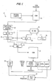
- Referring to Fig. 1, there is shown a block diagram implementation of a
microsequencer circuit 10 in accordance with the principles of the invention. Aprogram counter 12 facilitates the sequential execution of a plurality of program instruction stored in a random access memory (RAM) 14. A primary microinstruction group, which includes a plurality of microinstructions, is stored in a control store memory such as a read only memory (ROM) or a programmed logic array (PLA) 16. Additionally, a micro subroutine group, which includes a plurality of subroutines each containing a plurality of microinstructions associated with the respective subroutine, is stored inROM 16. Each of the stored microinstructions includes a field of control bits which may be fully encoded, practically encoded or unencoded. In addition, each microin struction includes a sequence field which specifies whether a selected microinstruction is to be succeeded by the next microinstruction in sequence or is either a conditional branch instruction, jump to subroutine instruction or return from subroutine instruction. - A selected program instruction is feed to an instruction register (IR) 18. An op code associated with the selected program instruction is then decoded by a
decoder circuit 20 in order to generate a microaddress which is associated with the op code. The microaddress is then loaded into afirst microprogram counter 22 which facilitates the sequential accessing of microinstructions stored in theROM 16. Thereafter, the microaddress contained in thefirst microprogram counter 22 is fed to an address register (not shown) associated with theROM 16. When theROM 16 is addressed by the current address in the address register, a corresponding microinstruction is read out in parallel and loaded into a control store data register (CSDR) 24. As noted above, each of the microinstructions stored in theROM 16 includes a plurality of fields. These fields are used to activate or enable a digital device to being controlled such as theinstruction register 18, aninstruction unit 26 andlogic circuit 28. Thefirst microprogram counter 22 is then incremented to address the next sequentially stored microinstruction. - Alternately, when a particular microinstruction is accessed and indicates that a subroutine will be the next program to be executed, the CSDR 24 facilitates the disabling of the
first microprogram counter 22, the enabling of thesecond microprogram counter 30 and a switching of themultiplexer 32 to the second microprogram counter. Themicroprogram counter 22 retains the last microaddress stored therein as a branched-from address. The branched-from address is associated with the microinstruction which called the subroutine. Theinstruction unit 26 facilitates the loading of an address associated with the first microinstruction of the subroutine into thesecond microprogram counter 30. Thereafter, thesecond microprogram counter 30 is incremented to facilitate sequential addressing of microinstructions associated with the subroutine being executed. When the subroutine has been fully executed, the CSDR 24 facilitates the re-enabling of thefirst microprogram counter 22, the disabling of thesecond microprogram counter 30 and the switching of themultiplexer 32 to the first microprogram counter. Thefirst microprogram counter 22 is then incremented so that the next program instruction is executed in a sequential orderly manner. - Referring to Fig. 2, there is shown a logical implementation of the
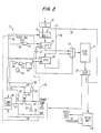
microsequencer 10. As noted above a program instruction is loaded into theinstruction register 18. The op code associated with this instruction is decoded by thedecoder circuit 20 and a starting address is loaded into thefirst program counter 22 when theinstruction unit 26 generates a "fetch load clock signal." The starting address is then fed throughmultiplexer 22 to theROM 16. Thereafter, the addressed microinstruction is loaded into theCSDR 24. If the microinstruction loaded into theCSDR 24 is not a subroutine call, a logic zero is fed to thelogic circuit 28 overlines jump logic circuit 38 then generates a logic zero on itsoutput line 40.Lines AND gate 42 which facilitate the generation of a logic zero onoutput line 44. The logic zero appearing onoutput 44 is fed to an input of a D-type flip flop 46 throughNOR gates 48 and 50. A logic zero, which then appears on an output offlip flop 46, is fed to an output of aninverter 52 in order to enable the incrementing of thefirst microprogram counter 22. The microinstructions stored in theROM 16 are then addressed sequentially by themicroprogram counter 22 until a subroutine call or jump instruction is encounter or a microinstruction is encountered which represents an "end of operation" (ENDOP). - If the microinstruction which was loaded into the
CSDR 24 is a subroutine call, a logic one is fed to thelogic circuit 28 over each of thelines jump logic circuit 38 generates a logic one on itsoutput line 40. A logic one now appears onoutput line 44 which enables thesecond microprogram counter 30 to load an address appearing onlines line 44 is fed through NORgates 48 and 50 to the input offlip flop 46.Flip flop 46 then generates a logic one on its output which disables thefirst microprogram counter 22 and enables thesecond microprogram counter 30. Thesecond microprogram counter 30 then sequentially accesses microinstructions associated with subroutine until a microinstruction is accessed which represents a subroutine return. Thereafter, theCSDR 24 feeds a signal representing the subroutine return to an input of an ANDgate 58 which causes aflip flop 46 to generate a logic zero on its output. The logic zero appearing on the output of theflip flop 46 facilitates the enabling and incrementing of thefirst microprogram counter 22 and the disabling of thesecond microprogram counter 30. Thus, thefirst microprogram counter 22 then proceeds to sequentially access microinstructions stored in theROM 16 until the ENDOP statement or another subroutine call is encountered. - Alternately, the microinstruction loaded in the
CSDR 24 may represent a conditional or unconditional jump instruction. TheCSDR 24 then feeds a logic one overline 34 and logic zero overline 36 to thelogic circuit 28. TheCSDR 24 also feeds conditional jump signals to thejump logic circuit 38 overline 59.Line 34 is coupled to and feeds the logic one to inputs of ANDgates gate 42 and throughinverter 64 to an input of ANDgate 62. Thejump logic circuit 38 then generates a logic one onoutput line 40 if the jump instruction is an unconditional jump instruction or, if the jump instruction is conditional, when the desired condition generated by the processor has occurred. A logic one now appears on theoutput line 66 of the ANDgate 60 if all of its inputs are of logic one.Output line 66 is coupled to and feeds the logic one to an input of ANDgate 62 andOR gate 67. The ANDgate 62 then generates a logic one onoutput line 68 which is then fed to amultiplexer 70.Multiplexer 70 in, response to the logic one appearing onoutput line 68, switches its input fromposition 0 to position 1. TheCSDR 24 feeds a next instruction or a jump address to a second input of themultiplexer 70 overline microprogram counter 22 is enabled to load the next address by the logic one appearing on theoutput line 66.Micro program counter 22 then sequentially accesses microinstructions stored in theROM 16 beginning with the "next instruction or jump address." - Referring again to Fig. 1, the
microsequencer circuit 10 may also include a plurality of microprogram counters 74 each having input coupled to respective outputs of ademultiplexer circuit 76. The plurality of microprogram counters 74 facilitates the nesting of subroutines. If themicrosequencer circuit 10 is executing a first subroutine and a subroutine call to a second subroutine is encountered, a branched-from address is stored in thesecond microprogram counter 30 and a starting of address is loaded into a selected one of the plurality of microprogram counters 74 under the control of thelogic circuit 28. The selected one of the plurality of microprogram counters 74 then sequentially addresses the instructions associated with the second subroutine. Whenever the second subroutine has been executed, thelogic circuit 28 then re-enables microprogram counter 30 to sequentially address the remaining instructions of the first subroutine. The number of subroutines which can be nested using this technique is limited to the number of microprogram counters included in the plurality of microprogram counters 74. - Referring to Fig. 3, there is shown a alternate embodiment of a
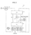
microsequencer circuit 80 which utilizes associative memory techniques to establish a starting address. Themicrosequencer circuit 80 includes two PLAs' 82 and 84. An op code which associated with a program instruction, is fed through a multiplexer/decoder circuit 86 to an input ofPLA 82.PLA 82 then decodes the op code and generates a starting address. A predetermined number of bits of the starting address are fed directly to an input ofPLA 84 over abus 88. The remaining bits of the starting address which are loaded into afirst microprogram counter 90, are also fed to a second input ofPLA 84. Thus,PLA 82 serves as an associative memory element which specifies a first, of a sequence, of addresses for each program instruction and for each microbranch, microcall and microsubroutine set of microcodes stored inPLA 84.PLA 84 includes a series of sequences of microcode which execute or generate a control word for each of the program instructions, micro branches, microcalls and microsubroutines. - The control words generated by the
PLA 84 are sequentially loaded into a control store data register (CSDR) 92. Each of the control words includes a control field which facilitates the operation of thefirst microprogram counter 90 and asecond microprogram counter 94. As noted above thePLA 82 designates the starting address inPLA 84 and thefirst microprogram counter 90 sequences or counts through the microinstructions associated with the selected op codes. If during the sequencing by thefirst microprogram counter 90, a microsubroutine is encountered, the first microprogram counter is disabled and the second second microprogram counter is reset, loaded with a branch/next address stored in theCSDR 92 and enabled to sequence through the microinstructions of the microsubroutine. Moreover, the address of the microsubroutine is a combination of the address appearing onbus 88, the contents of afirst microprogram counter 90 and the contents of asecond microprogram counter 94. This technique results in a control word have a fewer number of bits. For purposes of the illustration and not of limitation, let us assume that it takes ten bits to addressPLA 84 additionally, assume that four bits of the starting address are placed onbus 88 byPLA 82, thefirst microprogram counter 90 is three bits wide and thesecond program counter 94 is three bits wide. In this manner, the next address field of the control word is required to be only three bits wide. The remainder of the address bits are generated by thePLA 82.
Claims (18)
characterized by:
a first microinstruction counter having an input connected to the output of said microprogram instruction memory, for receiving an address value corresponding to the initial microinstruction of a primary microinstruction group in said control store memory;
a N-to-1 multiplexer having a first input connected to the output of said first microinstruction counter, having a control input, and having an output connected as the address input to said control store memory;
said control store memory having a primary microinstruction group which includes a plurality of microinstructions, at least one of which includes a destination address field and a subroutine calling field, said control store memory further including a first micro subroutine group consisting of a plurality of microinstructions with a first microinstruction which is addressed by said destination address field of said primary microinstruction group and which further has a subroutine completion field, said control store memory further including a next micro subroutine group whose first microinstruction is addressed by a destination address field in said first micro subroutine group and which further includes a subroutine completed field;
a control store data register having an input connected to the output of said control store memory and having a first output for said subroutine call and said subroutine completion fields connected to said control input of said multiplexer;
a next microinstruction counter having an input connected to a second output of said control store data register for receiving the destination address field output from said control store memory, said next microinstruction counter having an output connected to a next input of said multiplexer;
a logic circuit connected between said first output of said control store data register and said control input of said multiplexer, for controlling, in response to said primary microinstruction group generating a subroutine in said subroutine call field, said multiplexer to disable the output of said first microinstruction counter and enable the output of said next microinstruction counter substantially concurrently with the outputting of a destination address from said primary microinstruction group over said second microinstruction counter, supplying the address for the first microinstruction in the first micro subroutine group stored in said control store memory;
whereby a branched-from microinstruction address is stored in said first microinstruction counter while said first micro subroutine group is being executed.
characterized by
are a plurality of N microinstruction counters having outputs applied to said multiplexer, said multiplexer having the logic circuit applying a control input thereto and the second through Nth of said microinstruction counters being connected through a demultiplexer to said second output of said control store data register, whereby a plurality of N nested sets of subroutines can be accommodated.
characterized by:
memory means for storing a plurality of instructions therein;
a first means, coupled to the memory means, for addressing instructions stored therein;
a second means, coupled to the memory means, for addressing instructions associated with a selected subroutine stored therein;
means, coupled to the memory means, for selectively enabling the first addressing means and the second addressing means;
multiplexer means, responsive to the enabling means, for selectively coupling the first addressing means and the second addressing means to the memory means;
whereby a branched-from address is stored in the first addressing means and a starting address of the selected subroutine is loaded in the second addressing means during the execution of the selected subroutine, the storing and the loading of the branched-from address and the starting address, respectively, occur simultaneously during a single instruction cycle, the second addressing means then sequentially access the instructions in the selected subroutine until the subroutine has been executed, thereafter the first addressing means is re-enabled.
characterized by
enabling means including:
a data register coupled to the memory means for storing an instruction addressed by the first addressing means and the second addressing means; and
a logic circuit means, responsive to the instruction stored in the data register, for controlling the first addressing means, the multiplexer means and the second addressing means.
characterized in
that the first addressing means is a first microprogram counter.
characterized in
that the second addressing means is a second microprogram counter.
characterized in
that the memory means is a read only memory.
characterized in
that the memory means is a programmed logic array.
characterized by:
a first programmed logic means for generating an address associated with an op code of an instruction;
a first counter means, coupled to the first programmed logic means, for generating an address associated with microcode with a plurality of instructions;
a second programmed logic means for storing sequences of microcode associated with a plurality of instructions;
a second counter means, coupled to the first programmed logic means, for generating an address associated with microcode contained in a selected subroutine;
means, coupled to the second programmed logic means, for enabling the operation of the first and the second counter means;
means coupled to the second programmed logic means, for feeding a branch/next address to the first programmed logic means; and
whereby the first programmed logic means and the first counter means combine to generate the address and sequentially access selected sequence of microcode stored in the second programmed logic circuit and whereby in response to the selected subroutine being addressed, the first programmed logic means, the first counter means and the second counter means combine to generate the address and sequentially access sequences of microcode associated with the selected subroutine stored in the second programmed logic circuit.
characterized in
that the first logic circuit is a programmed logic array.
characterized in
that the second logic circuit is a programmed logic array.
characterized in
that the feeding means is a control store data register.
characterized by:
memory means for storing a plurality of instructions therein;
a plurality of addressing means, coupled to the memory means, for addressing instructions stored therein;
means, coupled to the memory means, for selectively enabling one of the plurality of addressing means;
multiplexer means, responsive to the enabling means, for coupling a selected one the plurality of addressing means to the memory means; and
whereby a branched-from address is stored in a first of the plurality of addressing means and a starting address of a selected subroutine stored in the memory means is loaded in a second of the plurality of addressing means during the execution of the selected subroutine, the storing and the loading of the branched-from address and the starting address, respectively, occurs simultaneously during a single instruction cycle, the second of the plurality of addressing means then sequentially accesses the instructions associated with a selected subroutine stored in the memory means until the subroutine has been executed, thereafter the first of the plurality of addressing means is re-enabled.
characterized by
a demultiplexer means coupled between the memory means and the inputs of the second and subsequent addressing means.
characterized in
that the enabling means includes:
a data register coupled to the memory means for storing an instruction addressed by the plurality of addressing means; and
a logic circuit means, responsive to the instruction stored in the data register, for controlling the plurality of addressing means, the multiplexer means and the demultiplexer means.
characterized in
that each of the plurality of addressing means is a microprogram counter.
characterized in
that the memory means is a read only memory.
characterized in
that the memory means is a programmed logic array.
Applications Claiming Priority (2)
| Application Number | Priority Date | Filing Date | Title |
|---|---|---|---|
| US937772 | 1986-12-04 | ||
| US06/937,772 US4821183A (en) | 1986-12-04 | 1986-12-04 | A microsequencer circuit with plural microprogrom instruction counters |
Publications (2)
| Publication Number | Publication Date |
|---|---|
| EP0269911A2 true EP0269911A2 (en) | 1988-06-08 |
| EP0269911A3 EP0269911A3 (en) | 1990-12-19 |
Family
ID=25470377
Family Applications (1)
| Application Number | Title | Priority Date | Filing Date |
|---|---|---|---|
| EP19870116405 Withdrawn EP0269911A3 (en) | 1986-12-04 | 1987-11-06 | A microsequencer circuit |
Country Status (3)
| Country | Link |
|---|---|
| US (1) | US4821183A (en) |
| EP (1) | EP0269911A3 (en) |
| JP (1) | JPS63226732A (en) |
Families Citing this family (17)
| Publication number | Priority date | Publication date | Assignee | Title |
|---|---|---|---|---|
| US4991080A (en) * | 1986-03-13 | 1991-02-05 | International Business Machines Corporation | Pipeline processing apparatus for executing instructions in three streams, including branch stream pre-execution processor for pre-executing conditional branch instructions |
| US5148531A (en) * | 1988-03-31 | 1992-09-15 | Sharp Kabushiki Kaisha | System for executing a conditional statement without reading program data part that does not satisfy the conditional clause |
| JPH06105432B2 (en) * | 1989-06-01 | 1994-12-21 | 三菱電機株式会社 | Microprocessor |
| US5430862A (en) * | 1990-06-29 | 1995-07-04 | Bull Hn Information Systems Inc. | Emulation of CISC instructions by RISC instructions using two pipelined stages for overlapped CISC decoding and RISC execution |
| US5280595A (en) * | 1990-10-05 | 1994-01-18 | Bull Hn Information Systems Inc. | State machine for executing commands within a minimum number of cycles by accomodating unforseen time dependency according to status signals received from different functional sections |
| US5371864A (en) * | 1992-04-09 | 1994-12-06 | International Business Machines Corporation | Apparatus for concurrent multiple instruction decode in variable length instruction set computer |
| JP3211423B2 (en) * | 1992-10-13 | 2001-09-25 | ソニー株式会社 | Branch instruction execution method and branch instruction execution device |
| US5388233A (en) * | 1993-04-30 | 1995-02-07 | Intel Corporation | Method and apparatus for counting instruction types using bit masks and a programmable bit map |
| US6006321A (en) * | 1997-06-13 | 1999-12-21 | Malleable Technologies, Inc. | Programmable logic datapath that may be used in a field programmable device |
| US6150836A (en) * | 1997-06-13 | 2000-11-21 | Malleable Technologies, Inc. | Multilevel logic field programmable device |
| US6263429B1 (en) * | 1998-09-30 | 2001-07-17 | Conexant Systems, Inc. | Dynamic microcode for embedded processors |
| DE19905510A1 (en) * | 1999-02-10 | 2000-08-31 | Siemens Ag | Microprocessor and method for addressing in a microprocessor |
| US6438569B1 (en) | 1999-09-20 | 2002-08-20 | Pmc-Sierra, Inc. | Sums of production datapath |
| US7162621B2 (en) * | 2001-02-21 | 2007-01-09 | Mips Technologies, Inc. | Virtual instruction expansion based on template and parameter selector information specifying sign-extension or concentration |
| EP1622009A1 (en) * | 2004-07-27 | 2006-02-01 | Texas Instruments Incorporated | JSM architecture and systems |
| US9191211B2 (en) * | 2009-02-27 | 2015-11-17 | Atmel Corporation | Data security system |
| US9361109B2 (en) * | 2010-05-24 | 2016-06-07 | Qualcomm Incorporated | System and method to evaluate a data value as an instruction |
Citations (2)
| Publication number | Priority date | Publication date | Assignee | Title |
|---|---|---|---|---|
| FR2472782A1 (en) * | 1979-12-27 | 1981-07-03 | Cii Honeywell Bull | Stack management for sub program return addresses in microprogram - holds sub program return in last in first out register stack accessed through stack pointer |
| US4323963A (en) * | 1979-07-13 | 1982-04-06 | Rca Corporation | Hardware interpretive mode microprocessor |
Family Cites Families (21)
| Publication number | Priority date | Publication date | Assignee | Title |
|---|---|---|---|---|
| GB1218406A (en) * | 1968-07-04 | 1971-01-06 | Ibm | An electronic data processing system |
| US3593313A (en) * | 1969-12-15 | 1971-07-13 | Computer Design Corp | Calculator apparatus |
| IT995721B (en) * | 1973-10-10 | 1975-11-20 | Honeywell Inf Systems Italia | EQUIPMENT FOR THE INTERPRETATION OF FUNCTION CODES IN MICROPROGRAMMED COMPUTERS AND FOR THE INDEPENDENT ADDRESSING OF INTERPRETATIVE AND EXECUTIVE PHASES OF MICRO PROGRAM |
| US3978454A (en) * | 1974-06-20 | 1976-08-31 | Westinghouse Electric Corporation | System and method for programmable sequence control |
| US3967104A (en) * | 1974-11-26 | 1976-06-29 | Texas Instruments Incorporated | Direct and indirect addressing in an electronic digital calculator |
| US4038643A (en) * | 1975-11-04 | 1977-07-26 | Burroughs Corporation | Microprogramming control system |
| US4003033A (en) * | 1975-12-22 | 1977-01-11 | Honeywell Information Systems, Inc. | Architecture for a microprogrammed device controller |
| IT1123613B (en) * | 1976-10-07 | 1986-04-30 | Sits Soc It Telecom Siemens | MICROPROGRAM CONTROL UNIT FOR DATA PROCESSORS |
| US4159520A (en) * | 1977-01-03 | 1979-06-26 | Motorola, Inc. | Memory address control device with extender bus |
| US4099229A (en) * | 1977-02-14 | 1978-07-04 | The United States Of America As Represented By The Secretary Of The Navy | Variable architecture digital computer |
| US4179737A (en) * | 1977-12-23 | 1979-12-18 | Burroughs Corporation | Means and methods for providing greater speed and flexibility of microinstruction sequencing |
| US4370729A (en) * | 1980-03-21 | 1983-01-25 | Point 4 Data Corporation | Microprogram sequencer |
| US4348724A (en) * | 1980-04-15 | 1982-09-07 | Honeywell Information Systems Inc. | Address pairing apparatus for a control store of a data processing system |
| IT1149809B (en) * | 1980-06-12 | 1986-12-10 | Honeywell Inf Systems | SEQUENCER FOR MICROPROGRAMMED CONTROL UNIT |
| US4438492A (en) * | 1980-08-01 | 1984-03-20 | Advanced Micro Devices, Inc. | Interruptable microprogram controller for microcomputer systems |
| IT1134780B (en) * | 1980-12-18 | 1986-08-13 | Honeywell Inf Systems | MICROPROGRAMMED CONTROL UNIT WITH MULTIPLE JUMP NETWORK |
| JPS57153339A (en) * | 1981-03-18 | 1982-09-21 | Hitachi Ltd | Information processor |
| JPS57161941A (en) * | 1981-03-30 | 1982-10-05 | Fujitsu Ltd | Data processing device |
| US4439827A (en) * | 1981-12-28 | 1984-03-27 | Raytheon Company | Dual fetch microsequencer |
| US4551798A (en) * | 1982-11-03 | 1985-11-05 | Burroughs Corporation | Multiple control stores in a pipelined microcontroller for handling nester subroutines |
| US4546431A (en) * | 1982-11-03 | 1985-10-08 | Burroughs Corporation | Multiple control stores in a pipelined microcontroller for handling jump and return subroutines |
-
1986
- 1986-12-04 US US06/937,772 patent/US4821183A/en not_active Expired - Fee Related
-
1987
- 1987-11-06 EP EP19870116405 patent/EP0269911A3/en not_active Withdrawn
- 1987-12-04 JP JP62306090A patent/JPS63226732A/en active Pending
Patent Citations (2)
| Publication number | Priority date | Publication date | Assignee | Title |
|---|---|---|---|---|
| US4323963A (en) * | 1979-07-13 | 1982-04-06 | Rca Corporation | Hardware interpretive mode microprocessor |
| FR2472782A1 (en) * | 1979-12-27 | 1981-07-03 | Cii Honeywell Bull | Stack management for sub program return addresses in microprogram - holds sub program return in last in first out register stack accessed through stack pointer |
Also Published As
| Publication number | Publication date |
|---|---|
| JPS63226732A (en) | 1988-09-21 |
| US4821183A (en) | 1989-04-11 |
| EP0269911A3 (en) | 1990-12-19 |
Similar Documents
| Publication | Publication Date | Title |
|---|---|---|
| EP0269911A2 (en) | A microsequencer circuit | |
| US3949370A (en) | Programmable logic array control section for data processing system | |
| US3800293A (en) | Microprogram control subsystem | |
| US3988719A (en) | Microprogrammed data processing systems | |
| EP0124597B1 (en) | Multiple control stores in a pipelined microcontroller for handling jump and return subroutines | |
| US3978456A (en) | Byte-by-byte type processor circuit | |
| US3990054A (en) | Microprogram organization techniques | |
| US3560933A (en) | Microprogram control apparatus | |
| US4045782A (en) | Microprogrammed processor system having external memory | |
| JPS6114535B2 (en) | ||
| EP0055392B1 (en) | Microprogrammed control unit with multiple branch capability | |
| US4251862A (en) | Control store organization in a microprogrammed data processing system | |
| US3996566A (en) | Shift and rotate circuit for a data processor | |
| US3602889A (en) | Extended addressing for programmed data processor having improved register loading means | |
| US4370729A (en) | Microprogram sequencer | |
| GB1594014A (en) | Microprogramme system with fixed jump addressing | |
| US4429361A (en) | Sequencer means for microprogrammed control unit | |
| US4754393A (en) | Single-chip programmable controller | |
| US5032983A (en) | Entry point mapping and skipping method and apparatus | |
| EP0073561B1 (en) | High speed microinstruction execution apparatus | |
| EP0229734A2 (en) | Microprogram control device | |
| US4320454A (en) | Apparatus and method for operand fetch control | |
| US4160289A (en) | Microprogram-control unit for data processor | |
| US4674063A (en) | Information processing apparatus having a sequence control function | |
| US4661925A (en) | Computer control memory apparatus providing variable microinstruction length |
Legal Events
| Date | Code | Title | Description |
|---|---|---|---|
| PUAI | Public reference made under article 153(3) epc to a published international application that has entered the european phase |
Free format text: ORIGINAL CODE: 0009012 |
|
| AK | Designated contracting states |
Kind code of ref document: A2 Designated state(s): DE FR GB |
|
| 17P | Request for examination filed |
Effective date: 19881022 |
|
| PUAL | Search report despatched |
Free format text: ORIGINAL CODE: 0009013 |
|
| AK | Designated contracting states |
Kind code of ref document: A3 Designated state(s): DE FR GB |
|
| 17Q | First examination report despatched |
Effective date: 19930730 |
|
| STAA | Information on the status of an ep patent application or granted ep patent |
Free format text: STATUS: THE APPLICATION IS DEEMED TO BE WITHDRAWN |
|
| 18D | Application deemed to be withdrawn |
Effective date: 19931210 |
|
| RIN1 | Information on inventor provided before grant (corrected) |
Inventor name: HAURIS, JON E. |