EP0266832A1 - Fully digital phase-locked loop - Google Patents
Fully digital phase-locked loop Download PDFInfo
- Publication number
- EP0266832A1 EP0266832A1 EP87202058A EP87202058A EP0266832A1 EP 0266832 A1 EP0266832 A1 EP 0266832A1 EP 87202058 A EP87202058 A EP 87202058A EP 87202058 A EP87202058 A EP 87202058A EP 0266832 A1 EP0266832 A1 EP 0266832A1
- Authority
- EP
- European Patent Office
- Prior art keywords
- phase
- locked loop
- digital
- signal
- sampling
- Prior art date
- Legal status (The legal status is an assumption and is not a legal conclusion. Google has not performed a legal analysis and makes no representation as to the accuracy of the status listed.)
- Granted
Links
Images


Classifications
-
- H—ELECTRICITY
- H03—ELECTRONIC CIRCUITRY
- H03L—AUTOMATIC CONTROL, STARTING, SYNCHRONISATION, OR STABILISATION OF GENERATORS OF ELECTRONIC OSCILLATIONS OR PULSES
- H03L7/00—Automatic control of frequency or phase; Synchronisation
- H03L7/06—Automatic control of frequency or phase; Synchronisation using a reference signal applied to a frequency- or phase-locked loop
- H03L7/08—Details of the phase-locked loop
- H03L7/099—Details of the phase-locked loop concerning mainly the controlled oscillator of the loop
- H03L7/0991—Details of the phase-locked loop concerning mainly the controlled oscillator of the loop the oscillator being a digital oscillator, e.g. composed of a fixed oscillator followed by a variable frequency divider
Definitions
- the invention relates to a fully digital phase locked loop produced using a digital signal processor and comprising a sampler-blocker followed by an analog-digital converter and a filter assembly connected to the input. a decision logic whose output controls said sampler-blocker.
- Phase locked loops are used in the widest fields of telecommunications (radiolocation) as well as in metrology (frequency synthesis). The main property of these loops is to allow synchronization on a signal during noisy transmissions when the conventional detection means are inoperative in the face of the weak signal received.
- a digital phase locked loop as mentioned in the preamble is described in the article entitled “Digital Phase-Locked Loop Behavior with Clock and Sampler Quantization” by Carlos POLAMAZA-RAEZ and Clare D.McGtLLEM published in IEEE Transactions on Communications, voI.COM-33, N ° 8, August 1985, pages 753 to 759.
- the loop of the invention was implemented in a cryptophony equipment to ensure at reception the synchronization of the sampling of the scrambled digital speech signal.
- cryptographic equipment carrying out the interference by permutation of frequency sub-bands using digital processing. it is essential to find the exact synchronization of the samples on reception.
- the aim is to obtain an accelerated synchronization by using a double locking speed allowing a rapid approach at the start of convergence then a slower and more precise approach for the end of convergence and monitoring.
- phase-locked loop of the invention will be presented to the sampling synchronization of a scrambled digital signal by permutation of frequency sub-bands. After transmission, said signal is not directly usable as shown in the following analysis of its sampling phase.
- x b (n) be the digital scrambled signal transmitted and x b '(n) the digital scrambled signal after transmission by the analog channel.
- the value of D is not indifferent: indeed, after analysis of the signal x, the sub-band signals xc, x 1 , ..., x N-1 corresponding respectively to the sub -bands 0, 1, ..., N-1 must check: where me is an integer value, that is to say that we must find the sub-band signals as they were calculated with a delay.
- the signal z coming from the demodulator 4 is subtracted at 8 from the received signal in order to compensate for the elimination of the synchronization carrier.
- the sampling phase correction is carried out around the free frequency value (fe) by adding or removing a certain number of "machine" cycles from said processor.
- variable voltage of a VCO in an analog phase locked loop was thus replaced by a variation of "machine" cycles in the digital phase locked loop.
- fo fe / 4 as the frequency of the synchronization wave. This choice is not limiting and the processing performed when the frequency of the synchronization wave is f e / p will be explained below. p being an integer greater than 2.
- a signal for which f o , f e / 4 can be represented in digital form subsequently + A, 0, -A, 0, + A, 0, ... where A represents the peak amplitude of the wave synchronization.
- A represents the peak amplitude of the wave synchronization.
- At the reception can be represented subsequently 0, + 1 , 0, -1, 0. + 1 .... after sampling at f e and can be represented hereinafter + ⁇ , 0, - ⁇ , 0, + 1, 0, .... which particularly simplifies the demodulation operations.
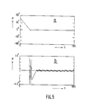
- FIG. 4a the evolution of the sampling phase error ⁇ during the acquisition is plotted, as a function of n, the sample considered.
- Figure 4c shows the evolution of the quantities
- and the az threshold ( ⁇ 1 4). The intersection of the two curves corresponds to the switching instant between fast approach and slow approach.
- phase error m is -135 °; a rapid convergence process begins, materialized by the linear part of Figure 4a.
- a second process begins, materialized in FIGS. 4a and 4b by oscillations around 0, caused by strong corrections affected by the sign of u (n).
- the phase ⁇ remaining however around 0.
- y (n) which corresponds to an energetic filtering of Asin ⁇ will approach zero, and a third process begins when we reach
- Figures 5a and 5b show a convergence in the case of an offset (5.10- 5 in relative value) of free frequency between wave synchronization and sampling.
- the larger phase oscillations around zero are produced by the need to permanently correct the local frequency.
- FIGS. 6a and 6b show the behavior of the loop in the presence of noise but without shifting the free frequencies, the signal to noise ratio being 28 dB. Thanks to the energetic filtering carried out by filters 5 and 6, the noise has very little influence on the sampling phase after convergence.
- Figures 7a and 7b show a convergence in the presence of noise and an offset free frequencies (signal to noise ratio: 28 dB, frequency offset: 5.10- 5 in relative value).
- the behavior of the loop is still acceptable with 20 dB signal to noise ratio and 10- 4 drift.
- the synchronization wave residue is weakened by at least 22 dB compared to the initial wave, which allows a frequency to be chosen located in the bandwidth of the channel (example: fe / 4. fe / 3, etc.).
- the locking loop operates in a completely analogous manner when the synchronization frequency is equal, no longer at f e / 4, but at f e / p (p> 2, p * 4).
- the sampled synchronization wave can be represented by Demodulators 3 and 4 use the signals respectively: and The sequences of the output states of 3 and 4 are respectively: u (n): Asin ⁇ ; -1/2 Asin ( ⁇ + 2 ⁇ / 3), -1/2 Asin ( ⁇ + 4 ⁇ / 3), ... v (n): 0, ⁇ 3 / 2 Asin ( ⁇ + 2 ⁇ / 3 ). -V3 / 2 Asin ( ⁇ + 4 ⁇ / 3), ...
- the filters calculate respectively:
Abstract
Description
L'invention concerne une boucle à verrouillage de phase entièrement numérique réalisée à l'aide d'un processeur numérique de signal et comportant un échantillonneur-bloqueur suivi d'un convertisseur analogique-numérique et d'un ensemble de filtrage relié à l'entrée d'une logique de décision dont la sortie commande ledit échantillonneur-bloqueur.The invention relates to a fully digital phase locked loop produced using a digital signal processor and comprising a sampler-blocker followed by an analog-digital converter and a filter assembly connected to the input. a decision logic whose output controls said sampler-blocker.
Les boucles à verrouillage de phase sont utilisées dans les domaines les plus vastes des télécommunications (radiolocalisation) ainsi qu'en métrologie (synthèse des fréquences). La propriété principale de ces boucles est de permettre la synchronisation sur un signal lors de transmissions bruitées lorsque les moyens classiques de détection sont inopérants face à la faiblesse du signal reçu. Une boucle à verrouillage de phase numérique telle que mentionnée dans le préambule est décrite dans l'article intitulé "Digital Phase-Locked Loop Behaviour with Clock and Sampler Quantization" par Carlos POLAMAZA-RAEZ et Clare D.McGtLLEM publié dans IEEE Transactions on Communications, voI.COM-33, N°8, Août 1985, pages 753 à 759.Phase locked loops are used in the widest fields of telecommunications (radiolocation) as well as in metrology (frequency synthesis). The main property of these loops is to allow synchronization on a signal during noisy transmissions when the conventional detection means are inoperative in the face of the weak signal received. A digital phase locked loop as mentioned in the preamble is described in the article entitled "Digital Phase-Locked Loop Behavior with Clock and Sampler Quantization" by Carlos POLAMAZA-RAEZ and Clare D.McGtLLEM published in IEEE Transactions on Communications, voI.COM-33, N ° 8, August 1985, pages 753 to 759.
La boucle de l'invention a été réalisée dans un équipement de cryptophonie pour assurer à la réception la synchronisation de l'échantillonnage du signal numérique de parole brouillé. Dans un tel équipement de cryptophonie réalisant le brouillage par permutations de sous-bandes de fréquence à l'aide d'un traitement numérique. il est fondamental de retrouver en réception la synchronisation exacte des échantillons.The loop of the invention was implemented in a cryptophony equipment to ensure at reception the synchronization of the sampling of the scrambled digital speech signal. In such cryptographic equipment carrying out the interference by permutation of frequency sub-bands using digital processing. it is essential to find the exact synchronization of the samples on reception.
Le but poursuivi est d'obtenir une synchronisation accélérée par utilisation d'une double vitesse de verrouillage permettant une approche rapide en début de convergence puis une approche plus lente et plus précise pour la fin de convergence et le suivi.The aim is to obtain an accelerated synchronization by using a double locking speed allowing a rapid approach at the start of convergence then a slower and more precise approach for the end of convergence and monitoring.
Conformément à l'invention ce but est atteint d'une manière optimale à l'aide des dispositions suivantes
- a) Ladite boucle à verrouillage de phase comporte à la suite dudit convertisseur analogique-numérique deux démodulateurs en quadrature fonctionnant à la fréquence de synchronisation et leurs filtres respectifs en sortie desquels un signal y tendant vers zéro après convergence et un signal z permettent de faire fonctionner la boucle en correction forte ou en correction fine selon que la valeur absolue de y est supérieure ou inférieure à une valeur de seuil.
- b) Ladite logique de décision effectue la correction de phase d'échantillonnage en retardant ou en avançant l'instant d'échantillonnage par l'ajout ou le retrait d'un certain nombre de cycles "machine" dudit processeur numérique.
- c) Un pilote de synchronisation étant inséré à l'émission dans le signal à transmettre, la boucle à verrouillage de phase numérique permet de retrouver une phase d'échantillonnage correcte de ce pilote.
- d) L'onde de synchronisation dudit pilote n'étant pas porteuse d'autre information est éliminée par compensation à l'aide de ladite boucle à verrouillage de phase. Cette disposition permet de placer l'onde de synchronisation en n'importe quelle partie de la bande passante notamment en utilisant une fréquence ayant un rapport simple avec la fréquence d'échantillonnage f, (exemple non limitatif : fe/3, fe/4, etc...).
- a) Said phase-locked loop comprises, following said analog-digital converter, two quadrature demodulators operating at the synchronization frequency and their respective filters at the output of which a signal tending towards zero after convergence and a signal z make it possible to operate the loop in strong correction or in fine correction depending on whether the absolute value of y is greater or less than a threshold value.
- b) Said decision logic performs the sampling phase correction by delaying or advancing the sampling instant by adding or removing a certain number of "machine" cycles from said digital processor.
- c) A synchronization pilot being inserted at transmission in the signal to be transmitted, the digital phase locked loop makes it possible to find a correct sampling phase of this pilot.
- d) The synchronization wave of said pilot not carrying any other information is eliminated by compensation using said phase-locked loop. This arrangement makes it possible to place the synchronization wave in any part of the pass band, in particular by using a frequency having a simple relationship with the sampling frequency f, (nonlimiting example: f e / 3, f e / 4, etc ...).
La description suivante en regard des dessins annexés le tout donné à titre d'exemple fera bien comprendre comment l'invention peut être réalisée.
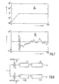
- La figure 1 montre le schéma de principe d'une boucle à verrouillage de phase entièrement numérique conforme à l'invention et fonctionnant à une fréquence de l'onde de synchronisation égale à fË4.
- La figure 2 indique les instants caractéristiques du programme réalisant la boucle.
- La figure 3 représente le schéma synoptique du traitement de correction.
- Les figures 4, 5, 6 et 7 montrent respectivement les résultats et l'analyse en simulation dans le cas idéal, avec dénve des oscillateurs, avec ajout de bruit et avec bruit et dérive.
- La figure 8 montre la modification apportée à la figure 1 dans le cas général où la fréquence de l'onde de synchronisation est égale à fe ip (p étant un entier supérieur à 2).
- Figure 1 shows the block diagram of a fully digital phase locked loop according to the invention and operating at a frequency of the synchronization wave equal to fË4.
- FIG. 2 indicates the characteristic moments of the program performing the loop.
- FIG. 3 represents the block diagram of the correction processing.
- Figures 4, 5, 6 and 7 respectively show the results and the simulation analysis in the ideal case, with deviation of the oscillators, with addition of noise and with noise and drift.
- FIG. 8 shows the modification made to FIG. 1 in the general case where the frequency of the synchronization wave is equal to f e ip (p being an integer greater than 2).
Dans la description ci-après, on va présenter l'application de la boucle à verrouillage de phase de l'invention à la synchronisation d'échantillonnage d'un signal numérique brouillé par permutation de sous-bandes de fréquences. Après transmission, ledit signal n'est pas directement exploitable ainsi que le montre l'analyse suivante de sa phase d'échantillonnage.In the description below, the application of the phase-locked loop of the invention will be presented to the sampling synchronization of a scrambled digital signal by permutation of frequency sub-bands. After transmission, said signal is not directly usable as shown in the following analysis of its sampling phase.
Soient xb(n) le signal brouillé numérique émis et xb'(n) le signal brouillé numérique après transmission par le canal analogique.Let x b (n) be the digital scrambled signal transmitted and x b '(n) the digital scrambled signal after transmission by the analog channel.
On suppose que le canal a une réponse impulsionnelle égale à δ(t-D). c'est-à-dire que le signal numérique à la réception est égal au signal numérique avant transmission retardé de D soit :![]()
![]()
Pour que le débrouillage se fasse correctement, la valeur de D n'est pas indifférente : en effet, après analyse du signal x, les signaux de sous-bande xc, x1,..., xN-1 correspondant respectivement aux sous-bandes 0, 1,..., N-1 doivent vérifier :![]()
![]()
Lors d'évaluations subjectives de la qualité de la parole restituée au débrouilleur de l'équipement de cryptophonie précité, on a constaté que la condition ci-dessus pouvait être réalisée avec une tolérance de 5 % de la période T sur la phase d'échantillonnage.During subjective evaluations of the quality of the speech returned to the descrambler of the aforementioned cryptophony equipment, it was found that the above condition could be fulfilled with a tolerance of 5% of the period T on the sampling phase .
Pour atteindre cet objectif, une boucle à verrouillage de phase entièrement numérique réalisée à l'aide d'un processeur de signal a été étudiée. Cette boucle dont le schéma de principe est représenté sur la figure 1, comporte les éléments constitutifs suivants:
- -un échantillonneur-
bloqueur 1 et un convertisseur analogique-numérique 2. - -deux démodulateurs en quadrature (cosinus et sinus) 3 et 4 et leurs filtres associés 5 et 6 fournissant respectivement les signaux y et z,
- -une logique de décision 7 permettant de faire la correction de phase d'échantillonnage.
- -a sampler-
blocker 1 and an analog-digital converter 2. - -two quadrature demodulators (cosine and sine) 3 and 4 and their associated filters 5 and 6 respectively supplying the signals y and z,
- a decision logic 7 making it possible to correct the sampling phase.
Le signal z provenant du démodulateur 4 est retranché en 8 du signal reçu afin d'éliminer par compensation la porteuse de synchronisation.The signal z coming from the
L'ensemble des éléments 3 à 8 est rassemblé dans le processeur de signal 9.All the
La correction de phase d'échantillonnage s'effectue autour de la valeur de fréquence libre (fe) par l'ajout ou le retrait d'un certain nombre de cycles "machine" dudit processeur.The sampling phase correction is carried out around the free frequency value (fe) by adding or removing a certain number of "machine" cycles from said processor.
Le réglage dans le temps du programme réalisant la boucle est illustré par la figure 2 sur laquelle les commandes d'échantillonnage agissant directement sur l'échantillonneur-bloqueur sont indiquées par les flèches Si (i = 1,2. 3...) et l'acquisition des échantillons par les flèches s; (i = 1, 2. 3...).The setting over time of the program performing the loop is illustrated in Figure 2 in which the sampling commands acting directly on the sampler-blocker are indicated by the arrows Si (i = 1,2. 3 ...) and acquisition of samples by arrows s ; (i = 1, 2. 3 ...).
Entre deux commandes successives d'échantillonnage, on trouve deux zones de durées fixes : une zone de latence A (i = 1, 2, 3 ...) pour l'acquisition de l'échantillon et une zone Bi (i = 1, 2, 3...) où s'effectue le calcul de la correction à appliquer pour chaque échantillon introduit à l'entrée de la boucle. Cette zone de correction est suivie d'une zone "tampon" Ci (i = 1, 2, 3...) de durée variable selon le résultat dudit calcul de correction.Between two successive sampling commands, there are two zones of fixed durations: a latency zone A (i = 1, 2, 3 ...) for the acquisition of the sample and a zone B i (i = 1 , 2, 3 ...) where the correction to be applied for each sample introduced at the loop input is calculated. This correction zone is followed by a "buffer" zone Ci (i = 1, 2, 3 ...) of variable duration according to the result of said correction calculation.
Ainsi par exemple, pour une période d'échantillonnage de 125 us (fe = 8 kHz) et pour un temps de cycle de processeur de 200 ns, on aurait un espacement de 125/0,2 = 625 cycles "machine" entre deux commandes successives d'échantillonnage si ladite correction était nulle c'est-à-dire si les fréquences du signal avant et après transmission étaient identiques. Ces fréquences étant différentes, le processeur élabore une correction et selon la valeur de cette correction un certain nombre d'unités sera retranché des 625 cycles "machine" calculés ci-dessus ou leur sera ajouté de façon à avancer ou à retarder la commande d'échantillonnage suivante.So for example, for a sampling period of 125 us (fe = 8 kHz) and for a processor cycle time of 200 ns, we would have a spacing of 125 / 0.2 = 625 "machine" cycles between two commands successive sampling if said correction was zero, that is to say if the frequencies of the signal before and after transmission were identical. These frequencies being different, the processor develops a correction and according to the value of this correction a certain number of units will be subtracted from the 625 "machine" cycles calculated above or will be added to them so as to advance or delay the command of next sampling.
On a ainsi remplacé la tension variable d'un VCO dans une boucle à verrouillage de phase analogique par une variation de cycles "machine" dans la boucle à verrouillage de phase numérique.The variable voltage of a VCO in an analog phase locked loop was thus replaced by a variation of "machine" cycles in the digital phase locked loop.
Pour simplifier au maximum les traitements, on a choisi fo = fe/4 comme fréquence de l'onde de synchronisation. Ce choix n'est pas limitatif et il sera expliqué ci-après les traitements réalisés lorsque la fréquence de l'onde de synchronisation est fe/p. p étant un entier supérieur à 2.To simplify the processing as much as possible, we chose fo = fe / 4 as the frequency of the synchronization wave. This choice is not limiting and the processing performed when the frequency of the synchronization wave is f e / p will be explained below. p being an integer greater than 2.
Un signal pour lequel fo, = f e/4 peut être représenté sous forme numérique par la suite +A, 0, -A, 0, + A, 0, ... où A représente l'amplitude crête de l'onde de synchronisation. A la réception,

Si l'onde de synchronisation est échantillonnée avec une erreur de phase φ, ladite onde peut être représentée par la suite Asin(2¶ x n fe/4 T + φ) = Asin(n ¶/2 + φ) où n est un indice courant désignant le numéro de l'échantillon considéré.If the synchronization wave is sampled with a phase error φ, said wave can be represented below Asin (2¶ xn fe / 4 T + φ) = Asin (n ¶ / 2 + φ) where n is an index current designating the number of the sample considered.
La suite des échantillons est la suivante : Asinφ, Acosφ, - Asinφ, - Acosφ, Asinφ,..., ce qui donne les suites suivantes :
- en sortie du démodulateur 4 : v(n) = 0, Acosφ, 0, Acosφ, 0,...
- en sortie du démodulateur 3 : u(n) = Asinφ, 0, Asinφ, 0, Asinφ,...
En sous-échantillonnant les sorties des démodulateurs et en ne gardant que les instants significatifs, c'est-à-dire en ignorant les multiplications par les zéros des démodulateurs, ces deux suites deviennent respectivement Acosφ, Acosφ, Acosφ.... et Asinφ, Asinφ, Asinφ,...The sequence of samples is as follows: Asinφ, Acosφ, - Asinφ, - Acosφ, Asinφ, ..., which gives the following sequences:
- at the output of demodulator 4: v (n) = 0, Acosφ, 0, Acosφ, 0, ...
- at the output of demodulator 3: u (n) = Asinφ, 0, Asinφ, 0, Asinφ, ...
By subsampling the outputs of the demodulators and keeping only the significant instants, that is to say by ignoring the multiplications by the zeros of the demodulators, these two sequences become respectively Acosφ, Acosφ, Acosφ .... and Asinφ , Asinφ, Asinφ, ...
Lors de la convergence de la boucle, la valeur de φ tendra vers 0, et lesdites suites tendront respectivement vers A. A, A,... et 0, 0, 0,...During the convergence of the loop, the value of φ will tend to 0, and said sequences will tend respectively to A. A, A, ... and 0, 0, 0, ...
A l'aide des signaux de sortie des cellules de filtrage situées après les démodulateurs (signaux appelés y et z), il est possible de faire fonctionner la boucle selon deux modes : acquisition rapide mais grossière, fin de convergence et suivi selon le schéma synoptique de la figure 3.Using the output signals of the filter cells located after the demodulators (signals called y and z), it is possible to operate the loop in two modes: rapid but coarse acquisition, end of convergence and monitoring according to the block diagram in Figure 3.
Sur ce synoptique, les fonctions d'échantillonnage et de conversion analogique-numérique du signal d'entrée x(t) représentées de manière distincte par 1 et 2 sur la figure 1 sont regroupées ici dans le bloc 1.2 indiquant en outre que seules les valeurs non nulles des échantillons sont exploitées et transmises aux démodulateurs locaux 3 et 4.In this diagram, the functions of sampling and analog-digital conversion of the input signal x (t) represented separately by 1 and 2 in FIG. 1 are grouped here in block 1.2, further indicating that only the values non-zero samples are processed and transmitted to
Les signaux u(n) et v(n) issus de ces démodulateurs sont ensuite filtrés à l'aide des filtres 5 et 6 passe- bas récursifs du premier ordre dont la réponse est donnée par :
En sortie des filtres numériques, on trouve les signaux y(n) et z(n). Les signaux u(n), y(n), z(n) vont servir à déterminer la correction à appliquer. En cas d'erreur de phase statique (ou variant lentement vis à vis des fréquences de coupure des filtres 5 et 6), y(n) tend vers Asinφ et z(n) tend vers Acoso.At the output of the digital filters, there are the signals y (n) and z (n). The signals u (n), y (n), z (n) will be used to determine the correction to be applied. In the event of a static phase error (or varying slowly with respect to the cutoff frequencies of filters 5 and 6), y (n) tends towards Asinφ and z (n) tends towards Acoso.
|y(n)| est d'abord comparé à un seuil défini par : seuil = αz(n), (a = 1/4).
- -si |y(n)| est supérieure au seuil, (N). cela signifie que le déphasage φ est important, et l'on va appliquer une forte correction (COFO) de la phase d'échantillonnage, cette correction consistant en une variation de 10 temps de cycle machine, le sens de la correction étant déterminé par le signe de u(n) :
- = si u(n)<0 (φ négatif), l'instant d'échantillonnage est retardé par l'ajout de 10 temps de cycles, ce qui tend à augmenter algébriquement φ, donc à le rapprocher de zéro.
- = si u(n)>0 (φ positif). l'instant d'échantillonnage est avancé, ce qui tend encore à rapprocher φ de 0.
- -si|y(n)| est inférieure au seuil, (Y), il est décidé d'appliquer une correction fine (COFI) de l'instant d'échantillonnage, qui consiste à faire varier ce dernier de un temps de cycle machine tous les p échantillons y(n) (exemple : p = 8, ou 16, ou 32 suivant la rapidité de correction désirée), le sens de la correction étant encore déterminé par le signe de u(n).
- -if | y (n) | is greater than the threshold, (N). this means that the phase shift φ is important, and a strong correction (COFO) of the sampling phase will be applied, this correction consisting of a variation of 10 machine cycle times, the direction of the correction being determined by the sign of u (n):
- = if u (n) <0 (φ negative), the sampling instant is delayed by the addition of 10 cycle times, which tends to increase algebraically φ, therefore bringing it closer to zero.
- = if u (n)> 0 (φ positive). the sampling instant is advanced, which still tends to bring φ closer to 0.
- -if | y (n) | is below the threshold, (Y), it is decided to apply a fine correction (COFI) of the sampling instant, which consists in varying the latter by a machine cycle time every p samples y (n) (example: p = 8, or 16, or 32 depending on the speed of correction desired), the direction of the correction being still determined by the sign of u (n).
Il n'est pas effectué de correction sur la valeur du signal z(n), comme indiqué (NOCO) sur le schéma synoptique de la figure 3.No correction is made to the value of the signal z (n), as indicated (NOCO) in the block diagram of FIG. 3.
Le comportement de la boucle en simulation a été analysé dans le cas idéal (voir figure 4).The behavior of the loop in simulation was analyzed in the ideal case (see Figure 4).
Sur la figure 4a on a tracé l'évolution de l'erreur de phase de l'échantillonnage φ lors de l'acquisition, en fonction de n, l'échantillon considéré.In FIG. 4a, the evolution of the sampling phase error φ during the acquisition is plotted, as a function of n, the sample considered.
On a porté sur la figure 4b un agrandissement de la courbe précédente entre ± 4.5° représentant l'écart de ± 5 % que l'on peut tolérer sur la période d'échantillonnage.An enlargement of the previous curve between ± 4.5 ° representing the difference of ± 5% which can be tolerated over the sampling period has been shown in FIG. 4b.
La figure 4c montre l'évolution des grandeurs |y| et du seuil az.(α = 1 4). L'intersection des deux courbes correspond à l'instant de commutation entre approche rapide et approche lente.Figure 4c shows the evolution of the quantities | y | and the az threshold (α = 1 4). The intersection of the two curves corresponds to the switching instant between fast approach and slow approach.
A la mise en route de la boucle numérique, l'erreur de phase m est de -135° ; un processus de convergence rapide s'engage, matérialisé par la partie linéaire de la figure 4a. Lorsque l'on atteint la phase 0, un deuxième processus s'engage, matérialisé sur les figures 4a et 4b par des oscillations autour de 0, provoquées par des corrections fortes affectées du signe de u(n). La phase φ restant toutefois autour de 0. y(n) qui correspond à un filtrage énergique de Asinφ va se rapprocher de zéro, et un troisième processus débute lorsque l'on atteint |y(n)|< seuil, ce processus étant la convergence finale à l'aide de corrections fines, ce qui est matérialisé par la partie quasi-linéaire de la figure 4b, suivie d'oscillations de faible amplitude au voisinage de zéro, produites par la quantification des corrections.When the digital loop is started, the phase error m is -135 °; a rapid convergence process begins, materialized by the linear part of Figure 4a. When one reaches
Les figures 5a et 5b montrent une convergence dans le cas d'un décalage (5.10-5 en valeur relative) de fréquence libre entre l'onde de synchronisation et l'échantillonnage. Les oscillations plus grandes de la phase autour de zéro sont produites par la nécessité de corriger la fréquence locale en permanence.Figures 5a and 5b show a convergence in the case of an offset (5.10- 5 in relative value) of free frequency between wave synchronization and sampling. The larger phase oscillations around zero are produced by the need to permanently correct the local frequency.
Les figures 6a et 6b présentent le comportement de la boucle en présence de bruit mais sans décalage des fréquences libres, le rapport signal à bruit étant de 28 dB. Grâce aux filtrages énergiques réalisés par les filtres 5 et 6, le bruit n'influence que très peu la phase d'échantillonnage après convergence.FIGS. 6a and 6b show the behavior of the loop in the presence of noise but without shifting the free frequencies, the signal to noise ratio being 28 dB. Thanks to the energetic filtering carried out by filters 5 and 6, the noise has very little influence on the sampling phase after convergence.
Les figures 7a et 7b montrent une convergence en présence de bruit et d'un décalage des fréquences libres (rapport signal à bruit : 28 dB, décalage des fréquences : 5.10-5 en valeur relative).Figures 7a and 7b show a convergence in the presence of noise and an offset free frequencies (signal to noise ratio: 28 dB, frequency offset: 5.10- 5 in relative value).
Le comportement de la boucle est encore acceptable avec 20 dB de rapport signal à bruit et 10-4 de dérive.The behavior of the loop is still acceptable with 20 dB signal to noise ratio and 10- 4 drift.
La précision de convergence permet de plus la suppression par compensation de la porteuse de synchronisation en sortie du dispositif. En effet, il s'agit de soustraire au signal reçu une onde sinusoïdale échantillonnée dont la phase est très proche de zéro, et dont l'amplitude est approximée par z(n) [z(n) = Acosφ # A quand m # 0]. Par soustraction de la suite 0, +A, 0. -A.... à la suite des échantillons reçus, on soustrait ainsi une sinusoïde

La boucle entièrement numérique ainsi réalisée présente les caractéristiques principales suivantes:
- -une acquisition rapide (= une centaine de périodes d'échantillonnage)
- -un suivi correct en présence de perturbations (bruit-dérive)
- -une réalisation simple sur processeur de signal.
- -une très bonne compensation de l'onde servant à la synchronisation.
- - rapid acquisition (= one hundred sampling periods)
- - correct monitoring in the presence of disturbances (noise-drift)
- -a simple realization on signal processor.
- -a very good compensation of the wave used for synchronization.
La boucle à verrouillage fonctionne de façon tout à fait analogue lorsque la fréquence de synchro- msation est éga le, non plus à fe/4, mais à fe/p (p> 2, p * 4). Dans ce cas le schéma de principe de la boucle à verrouillage de phase représenté sur la figure 1 doit être modifié conformément au schéma de la figure 8 en disposant devant les filtres récursifs 5 et 6 les filtres transverses 10 et 11 respectivement, comme il va être expliqué ci-après pour p = 3 à titre d'exemple non limitatif.The locking loop operates in a completely analogous manner when the synchronization frequency is equal, no longer at f e / 4, but at f e / p (p> 2, p * 4). In this case the block diagram of the phase-locked loop shown in FIG. 1 must be modified in accordance with the diagram in FIG. 8 by placing the transverse filters 10 and 11 in front of the recursive filters 10 and 11 respectively, as will be explained below for p = 3 by way of nonlimiting example.
L'onde de synchronisation échantillonnée peut être représentée par


On constate des variations d'amplitude périodiques de fréquence fe/3 (le même type de variations existait dans le cas p = 4, avec :
- u(n) = Asinφ, 0, Asinφ,...
- v(n) = 0, Acosφ, 0,..
mais elles étaient éliminées par le sous-échantillonnage).There are periodic amplitude variations of frequency f e / 3 (the same type of variations existed in the case p = 4, with:
- u (n) = Asinφ, 0, Asinφ, ...
- v (n) = 0, Acosφ, 0, ..
but they were eliminated by subsampling).
Ces variations d'amplitude sont éliminées à l'aide de filtres transverses 10 et 11 à p (= 3 dans notre exemple) coefficients égaux à 2/p (= 2'3 dans notre exemple).These amplitude variations are eliminated using transverse filters 10 and 11 at p (= 3 in our example) coefficients equal to 2 / p (= 2'3 in our example).
Les filtres calculent respectivement :

On est donc ramené au cas précédent, à condition d'utiliser u'(n) au lieu de u(n) dans le calcul de la correction. Lorsque l'asservissement converge, y(n) tend vers 0 et z(n) tend vers A, ce qui rend encore possible la compensation de l'onde de synchronisation par soustraction au signal reçu de la suite 0, Asin 2¶/p, Asin 4¶/p, Asin 6¶/p,...We are therefore brought back to the previous case, provided that u '(n) is used instead of u (n) in the calculation of the correction. When the servo converges, y (n) tends towards 0 and z (n) tends towards A, which still makes it possible to compensate for the synchronization wave by subtraction from the signal received from the
Claims (4)
Applications Claiming Priority (2)
| Application Number | Priority Date | Filing Date | Title |
|---|---|---|---|
| FR8615210 | 1986-10-31 | ||
| FR8615210A FR2606238B1 (en) | 1986-10-31 | 1986-10-31 | FULL DIGITAL PHASE LOCKED LOOP |
Publications (2)
| Publication Number | Publication Date |
|---|---|
| EP0266832A1 true EP0266832A1 (en) | 1988-05-11 |
| EP0266832B1 EP0266832B1 (en) | 1992-01-15 |
Family
ID=9340416
Family Applications (1)
| Application Number | Title | Priority Date | Filing Date |
|---|---|---|---|
| EP87202058A Expired - Lifetime EP0266832B1 (en) | 1986-10-31 | 1987-10-27 | Fully digital phase-locked loop |
Country Status (5)
| Country | Link |
|---|---|
| US (1) | US4969191A (en) |
| EP (1) | EP0266832B1 (en) |
| JP (1) | JPS63164531A (en) |
| DE (1) | DE3776082D1 (en) |
| FR (1) | FR2606238B1 (en) |
Cited By (1)
| Publication number | Priority date | Publication date | Assignee | Title |
|---|---|---|---|---|
| RU2599347C1 (en) * | 2015-03-27 | 2016-10-10 | Федеральное государственное казенное военное образовательное учреждение высшего профессионального образования "Военный учебно-научный центр Военно-воздушных сил "Военно-воздушная академия имени профессора Н.Е. Жуковского и Ю.А. Гагарина" (г. Воронеж) Министерства обороны Российской Федерации | Method of amplifying and demodulating frequency-modulated signals and device therefor |
Families Citing this family (2)
| Publication number | Priority date | Publication date | Assignee | Title |
|---|---|---|---|---|
| JP3113667B2 (en) * | 1990-05-30 | 2000-12-04 | 日本テキサス・インスツルメンツ株式会社 | Transversal filter circuit |
| JP3241079B2 (en) * | 1992-02-24 | 2001-12-25 | 株式会社日立製作所 | Digital phase locked loop |
Citations (4)
| Publication number | Priority date | Publication date | Assignee | Title |
|---|---|---|---|---|
| US3777272A (en) * | 1972-09-18 | 1973-12-04 | Nasa | Digital second-order phase-locked loop |
| EP0035166A1 (en) * | 1980-03-01 | 1981-09-09 | Licentia Patent-Verwaltungs-GmbH | Digital receiver |
| US4457003A (en) * | 1982-06-21 | 1984-06-26 | Motorola Inc. | Time reference tracking loop for frequency hopping systems |
| US4594555A (en) * | 1984-10-29 | 1986-06-10 | Hewlett-Packard Company | Frequency selective sampling detector |
Family Cites Families (13)
| Publication number | Priority date | Publication date | Assignee | Title |
|---|---|---|---|---|
| US4004237A (en) * | 1970-05-01 | 1977-01-18 | Harris Corporation | System for communication and navigation |
| US4028626A (en) * | 1973-01-18 | 1977-06-07 | Hycom Incorporated | Digital data receiver with automatic timing recovery and control |
| US3971996A (en) * | 1973-01-18 | 1976-07-27 | Hycom Incorporated | Phase tracking network |
| NL171215C (en) * | 1973-03-09 | 1983-02-16 | Trt Telecom Radio Electr | AUTOMATIC EQUALIZATION DEVICE FOR A DATA TRANSMISSION CHANNEL. |
| JPS5152264A (en) * | 1974-09-11 | 1976-05-08 | Sharp Kk | |
| US3962637A (en) * | 1974-11-11 | 1976-06-08 | Hycom Incorporated | Ultrafast adaptive digital modem |
| US4004226A (en) * | 1975-07-23 | 1977-01-18 | Codex Corporation | QAM receiver having automatic adaptive equalizer |
| US3978407A (en) * | 1975-07-23 | 1976-08-31 | Codex Corporation | Fast start-up adaptive equalizer communication system using two data transmission rates |
| FR2445078A1 (en) * | 1978-12-20 | 1980-07-18 | Ibm France | METHOD AND DEVICE FOR DETECTING A PSEUDO-RANDOM SEQUENCE OF TWO SYMBOLS IN A DATA RECEIVER USING QUADRATURE DOUBLE SIDE-CARRIER MODULATION |
| FR2445079A1 (en) * | 1978-12-20 | 1980-07-18 | Ibm France | METHOD AND DEVICE FOR DETECTING A PSEUDO-RANDOM SEQUENCE OF PHASE CHANGES OF 0O AND 180O OF THE CARRIER IN A DATA RECEIVER |
| US4237554A (en) * | 1979-03-01 | 1980-12-02 | Bell Telephone Laboratories, Incorporated | Coefficient tap leakage for fractionally-spaced equalizers |
| US4680621A (en) * | 1985-09-16 | 1987-07-14 | Tektronix, Inc. | Method and apparatus for variable phasing of periodic signals |
| JPS63252014A (en) * | 1987-04-08 | 1988-10-19 | Kokusai Denshin Denwa Co Ltd <Kdd> | Phase locked loop system |
-
1986
- 1986-10-31 FR FR8615210A patent/FR2606238B1/en not_active Expired
-
1987
- 1987-10-27 DE DE8787202058T patent/DE3776082D1/en not_active Expired - Fee Related
- 1987-10-27 EP EP87202058A patent/EP0266832B1/en not_active Expired - Lifetime
- 1987-10-29 JP JP62271954A patent/JPS63164531A/en active Pending
- 1987-10-30 US US07/115,475 patent/US4969191A/en not_active Expired - Fee Related
Patent Citations (4)
| Publication number | Priority date | Publication date | Assignee | Title |
|---|---|---|---|---|
| US3777272A (en) * | 1972-09-18 | 1973-12-04 | Nasa | Digital second-order phase-locked loop |
| EP0035166A1 (en) * | 1980-03-01 | 1981-09-09 | Licentia Patent-Verwaltungs-GmbH | Digital receiver |
| US4457003A (en) * | 1982-06-21 | 1984-06-26 | Motorola Inc. | Time reference tracking loop for frequency hopping systems |
| US4594555A (en) * | 1984-10-29 | 1986-06-10 | Hewlett-Packard Company | Frequency selective sampling detector |
Non-Patent Citations (1)
| Title |
|---|
| IEEE TRANSACTIONS ON INDUSTRIAL ELECTRONICS AND CONTROL INSTRUMENTATION, vol. IECI-20, no. 4, novembre 1973, pages 239-251, New York, US; C.P. REDDY et al.: "A class of all digital phase locked loops: Modeling and analysis" * |
Cited By (1)
| Publication number | Priority date | Publication date | Assignee | Title |
|---|---|---|---|---|
| RU2599347C1 (en) * | 2015-03-27 | 2016-10-10 | Федеральное государственное казенное военное образовательное учреждение высшего профессионального образования "Военный учебно-научный центр Военно-воздушных сил "Военно-воздушная академия имени профессора Н.Е. Жуковского и Ю.А. Гагарина" (г. Воронеж) Министерства обороны Российской Федерации | Method of amplifying and demodulating frequency-modulated signals and device therefor |
Also Published As
| Publication number | Publication date |
|---|---|
| JPS63164531A (en) | 1988-07-07 |
| US4969191A (en) | 1990-11-06 |
| FR2606238B1 (en) | 1988-12-09 |
| EP0266832B1 (en) | 1992-01-15 |
| FR2606238A1 (en) | 1988-05-06 |
| DE3776082D1 (en) | 1992-02-27 |
Similar Documents
| Publication | Publication Date | Title |
|---|---|---|
| EP0036084B1 (en) | Process and device for the control of the initial adjustment of the clock of a receiver for synchronous data | |
| EP0054829B1 (en) | Method and apparatus for detecting the training sequence of an autoadaptive equalizer | |
| EP0125722A1 (en) | Circuit for joint adaptive equalisation and demodulation | |
| EP0142440A2 (en) | Generating device for a frequency being a fraction of a reference frequency | |
| EP0716501B1 (en) | Phase comparator of a digital signal and a clock signal, and corresponding phase locked loop | |
| FR2568014A1 (en) | PULSE-SHAPED PULSE DETECTION DEVICE AND PULSE-SHAPED PULSE SUPPRESSION DEVICE WITH PULSE-SHAPED DEVICE DETECTION DEVICE | |
| EP0012884B1 (en) | Process and apparatus for detecting a pseudo-random sequence of two symbols in a data receiver using a double sideband modulation with quadrature carriers | |
| EP0266832B1 (en) | Fully digital phase-locked loop | |
| EP1782536B1 (en) | Method of generating a digital signal that is representative of match errors in an analogue-to-digital conversion system with time interleaving, and an analogue-to-digital converter with time interleaving using same | |
| EP0205150A1 (en) | Process and device for the reduction of the jitter of a synchronous digital pulse train to recover its rhythm | |
| EP0230900B1 (en) | Device for clock recovery | |
| FR2519818A1 (en) | PHASE LOCK LOOP AND METHOD FOR IMPROVING OUTPUT SIGNAL | |
| Poberezhskiy et al. | Sampling technique allowing exclusion of antialiasing filter | |
| EP0205373B1 (en) | Adjustable digital phase shifter and digital velocity compensator for a magnetoscope using it | |
| EP1940023A2 (en) | Bank of cascadable digital filters, and reception circuit including such a bank of cascaded filters | |
| WO1995022196A1 (en) | Continuous phase modulation device using a frequency synthesizer with a phase-locked loop | |
| EP0218508B1 (en) | Quickly variable frequency generator | |
| EP0035295A1 (en) | Clock phase control method for a digital data receiving system, phase recovery circuit for carrying out this method and digital data receiving system comprising this circuit | |
| EP0181808B1 (en) | Spectrum analyser using surface wave dispersion filters | |
| EP0461022B1 (en) | Apparatus for carrier recovery with means for preventing a false frequency lock | |
| EP0737868B1 (en) | Delay locked loop for use in a GPS receiver | |
| FR2908946A1 (en) | BVP DIGITAL FRACTIONAL | |
| FR2587498A1 (en) | Detector of digital phase and/or frequency over a wide range | |
| FR2485296A1 (en) | PROGRAMMABLE FREQUENCY ANALYZER DIGITAL CIRCUIT | |
| EP0031270B1 (en) | Filter device with low phase distortion and circuit comprising such a device for treating colour television signals |
Legal Events
| Date | Code | Title | Description |
|---|---|---|---|
| PUAI | Public reference made under article 153(3) epc to a published international application that has entered the european phase |
Free format text: ORIGINAL CODE: 0009012 |
|
| AK | Designated contracting states |
Kind code of ref document: A1 Designated state(s): DE FR GB IT SE |
|
| 17P | Request for examination filed |
Effective date: 19881021 |
|
| 17Q | First examination report despatched |
Effective date: 19910125 |
|
| RAP1 | Party data changed (applicant data changed or rights of an application transferred) |
Owner name: THOMSON-TRT DEFENSE |
|
| RAP1 | Party data changed (applicant data changed or rights of an application transferred) |
Owner name: THOMSON-TRT DEFENSE |
|
| GRAA | (expected) grant |
Free format text: ORIGINAL CODE: 0009210 |
|
| AK | Designated contracting states |
Kind code of ref document: B1 Designated state(s): DE FR GB IT SE |
|
| ITF | It: translation for a ep patent filed |
Owner name: JACOBACCI & PERANI S.P.A. |
|
| RAP2 | Party data changed (patent owner data changed or rights of a patent transferred) |
Owner name: THOMSON-TRT DEFENSE |
|
| REF | Corresponds to: |
Ref document number: 3776082 Country of ref document: DE Date of ref document: 19920227 |
|
| GBT | Gb: translation of ep patent filed (gb section 77(6)(a)/1977) | ||
| PG25 | Lapsed in a contracting state [announced via postgrant information from national office to epo] |
Ref country code: GB Effective date: 19921027 |
|
| PG25 | Lapsed in a contracting state [announced via postgrant information from national office to epo] |
Ref country code: SE Effective date: 19921028 |
|
| PLBE | No opposition filed within time limit |
Free format text: ORIGINAL CODE: 0009261 |
|
| STAA | Information on the status of an ep patent application or granted ep patent |
Free format text: STATUS: NO OPPOSITION FILED WITHIN TIME LIMIT |
|
| 26N | No opposition filed | ||
| GBPC | Gb: european patent ceased through non-payment of renewal fee |
Effective date: 19921027 |
|
| PG25 | Lapsed in a contracting state [announced via postgrant information from national office to epo] |
Ref country code: FR Effective date: 19930630 |
|
| PG25 | Lapsed in a contracting state [announced via postgrant information from national office to epo] |
Ref country code: DE Effective date: 19930701 |
|
| REG | Reference to a national code |
Ref country code: FR Ref legal event code: ST |
|
| EUG | Se: european patent has lapsed |
Ref document number: 87202058.1 Effective date: 19930510 |
|
| PG25 | Lapsed in a contracting state [announced via postgrant information from national office to epo] |
Ref country code: IT Free format text: LAPSE BECAUSE OF NON-PAYMENT OF DUE FEES;WARNING: LAPSES OF ITALIAN PATENTS WITH EFFECTIVE DATE BEFORE 2007 MAY HAVE OCCURRED AT ANY TIME BEFORE 2007. THE CORRECT EFFECTIVE DATE MAY BE DIFFERENT FROM THE ONE RECORDED. Effective date: 20051027 |